JP4496907B2 - Magnetic measurement circuit - Google Patents
Magnetic measurement circuit Download PDFInfo
- Publication number
- JP4496907B2 JP4496907B2 JP2004286891A JP2004286891A JP4496907B2 JP 4496907 B2 JP4496907 B2 JP 4496907B2 JP 2004286891 A JP2004286891 A JP 2004286891A JP 2004286891 A JP2004286891 A JP 2004286891A JP 4496907 B2 JP4496907 B2 JP 4496907B2
- Authority
- JP
- Japan
- Prior art keywords
- signal
- voltage
- output
- measurement
- switches
- Prior art date
- Legal status (The legal status is an assumption and is not a legal conclusion. Google has not performed a legal analysis and makes no representation as to the accuracy of the status listed.)
- Expired - Fee Related
Links
- 238000005259 measurement Methods 0.000 title claims description 67
- 230000005389 magnetism Effects 0.000 claims 1
- 230000001360 synchronised effect Effects 0.000 claims 1
- 239000003990 capacitor Substances 0.000 description 38
- 238000010586 diagram Methods 0.000 description 13
- 239000004065 semiconductor Substances 0.000 description 13
- 230000003321 amplification Effects 0.000 description 10
- 238000003199 nucleic acid amplification method Methods 0.000 description 10
- 238000006243 chemical reaction Methods 0.000 description 9
- 230000007274 generation of a signal involved in cell-cell signaling Effects 0.000 description 6
- 229920000371 poly(diallyldimethylammonium chloride) polymer Polymers 0.000 description 4
- 230000000694 effects Effects 0.000 description 3
- 238000000034 method Methods 0.000 description 2
- ATCJTYORYKLVIA-SRXJVYAUSA-N vamp regimen Chemical compound O=C1C=C[C@]2(C)[C@H]3[C@@H](O)C[C@](C)([C@@](CC4)(O)C(=O)CO)[C@@H]4[C@@H]3CCC2=C1.C=1N=C2N=C(N)N=C(N)C2=NC=1CN(C)C1=CC=C(C(=O)N[C@@H](CCC(O)=O)C(O)=O)C=C1.O([C@H]1C[C@@](O)(CC=2C(O)=C3C(=O)C=4C=CC=C(C=4C(=O)C3=C(O)C=21)OC)C(=O)CO)[C@H]1C[C@H](N)[C@H](O)[C@H](C)O1.C([C@H](C[C@]1(C(=O)OC)C=2C(=CC3=C(C45[C@H]([C@@]([C@H](OC(C)=O)[C@]6(CC)C=CCN([C@H]56)CC4)(O)C(=O)OC)N3C=O)C=2)OC)C[C@@](C2)(O)CC)N2CCC2=C1NC1=CC=CC=C21 ATCJTYORYKLVIA-SRXJVYAUSA-N 0.000 description 2
- 230000001174 ascending effect Effects 0.000 description 1
- 230000007423 decrease Effects 0.000 description 1
- 230000003247 decreasing effect Effects 0.000 description 1
- 230000005669 field effect Effects 0.000 description 1
- 230000010354 integration Effects 0.000 description 1
Images


Landscapes
- Measuring Magnetic Variables (AREA)
- Hall/Mr Elements (AREA)
Description
本発明は、測定時間の短縮を図った磁気測定回路に関する。 The present invention relates to a magnetic measurement circuit that shortens measurement time.
従来、現在位置における方位(地磁気)を求める磁気測定回路として、MR素子(磁気抵抗効果素子)またはGMR素子(巨大磁気抵抗効果素子)を用いた回路が知られている。この磁気測定回路は、X、Y、Z軸方向の各地磁気の強さを測定するX、Y、Z軸センサと、各センサの出力をディジタルデータに変換する積分型A/D(アナログ/ディジタル)コンバータを具備している。 Conventionally, a circuit using an MR element (magneto-resistance effect element) or a GMR element (giant magneto-resistance effect element) is known as a magnetic measurement circuit for obtaining an orientation (geomagnetism) at the current position. This magnetic measurement circuit includes an X, Y, and Z axis sensor that measures the strength of each magnetic field in the X, Y, and Z axis directions, and an integral A / D (analog / digital) that converts the output of each sensor into digital data. ) It has a converter.
図9は従来の磁気測定回路の要部の構成を示す回路図であり、この図において、100は4個のGMR素子をブリッジ接続して構成された磁気センサ、101は磁気センサ100の出力を増幅する増幅器、102はA/Dコンバータ、103はA/Dコンバータ102において使用されるレファランス電圧VR2、VR、VSTARTを発生するレファランス電圧発生回路である。また、A/Dコンバータ102において、SI、SA〜SDは半導体スイッチ、C1、C3はコンデンサ、104は演算増幅器、105はコンパレータ、106はスイッチSA〜SDを駆動するタイミング信号を制御回路(図示略)から出力されるクロックパルスCLKに基づいて生成するタイミング信号発生回路である。
FIG. 9 is a circuit diagram showing a configuration of a main part of a conventional magnetic measurement circuit. In this figure, 100 is a magnetic sensor configured by bridge-connecting four GMR elements, and 101 is an output of the
このような構成において、タイミング信号発生回路106から出力される信号に従ってスイッチSA、SDがONとされ、次いでスイッチSC、SBがONとされ、この動作がクロックパルスCLKに同期して繰り返される。これにより、演算増幅器104から階段状の比較電圧INTEGが出力され、コンパレータ105において増幅器101の出力VAMPと比較される。またこの時、制御回路はクロックパルスを内蔵のカウンタによってアップカウントする。そして、演算増幅器104の出力INTEGが増幅器の出力VAMPを越えると、比較器105の出力CMPが反転する。制御回路はこの信号CMPの反転を受け、カウンタのアップカウントを停止し、その時のカウント値を磁気センサ100の測定値として出力する。
In such a configuration, the switches SA and SD are turned on in accordance with the signal output from the timing
ところで、地磁気測定には、磁気変化による出力変化量は少ないがゼロ磁場での出力(オフセット)のばらつきが大きいという特性がある。このため、入力範囲が大きく、かつ、分解能が高い積分型A/Dコンバータが必要となり、測定時間が長くなる問題があった。
なお、従来の磁気測定回路に関する文献として特許文献1、2が知られている。
本発明は上記事情を考慮してなされたもので、その目的は、従来のものに比較し測定時間を大幅に短縮することができる磁気測定回路を提供することにある。 The present invention has been made in view of the above circumstances, and an object of the present invention is to provide a magnetic measurement circuit capable of greatly reducing the measurement time as compared with the conventional one.
この発明は上記の課題を解決するためになされたもので、本発明は、磁気の強さを測定する磁気センサと、前記磁気センサの出力を増幅する増幅手段と、所定のクロック数に対応する第1期間に、クロックパルスに同期して第1のステップ幅で単調増加する電圧を発生させ、その後の第2期間に、クロックパルスに同期して前記第1のステップ幅より小さい第2のステップ幅で前記第1期間終了時の電圧から単調増加する電圧を発生させる電圧発生手段と、前記第2期間の開始から、前記電圧発生手段の発生電圧値と前記増幅手段の出力電圧値とを所定の比率で加算した電圧値が閾値電圧値以上となるまで、クロックパルスをカウントし、カウント結果を前記磁気の強さを表すデータとして出力するカウント手段と、を具備することを特徴とする磁気測定回路である。
本発明は、上記の磁気測定回路において、前記所定のクロック数は、前記電圧発生手段の前記第1のステップ幅による発生電圧値と前記増幅手段の出力電圧値とを前記所定の比率で加算した電圧値が前記閾値電圧値を超えるのに必要なクロック数よりも所定クロック数少ないクロック数に設定されていることを特徴とする。
The present invention has been made to solve the above-described problems. The present invention corresponds to a magnetic sensor for measuring magnetic strength, amplification means for amplifying the output of the magnetic sensor, and a predetermined number of clocks. A voltage that monotonously increases with a first step width in synchronization with the clock pulse is generated in the first period, and a second step smaller than the first step width in synchronization with the clock pulse is generated in the subsequent second period. A voltage generation unit that generates a voltage that monotonically increases from the voltage at the end of the first period in width, and a voltage value generated by the voltage generation unit and an output voltage value of the amplification unit from the start of the second period are predetermined. until the voltage value obtained by adding a proportion of the threshold voltage value or more, and characterized in that counts clock pulses, comprising counting means for outputting the count result as the data representing the intensity of the magnetic, A magnetic measurement circuit that.
According to the present invention, in the magnetic measurement circuit, the predetermined number of clocks is obtained by adding a voltage value generated by the first step width of the voltage generation unit and an output voltage value of the amplification unit at the predetermined ratio. The voltage value is set to a number of clocks that is a predetermined number of clocks less than the number of clocks required to exceed the threshold voltage value.
本発明は、上記の磁気測定回路において、前記磁気センサはMR素子またはGMR素子によって構成されていることを特徴とする。 The present invention is characterized in that, in the magnetic measurement circuit described above , the magnetic sensor is constituted by an MR element or a GMR element .
この発明によれば、従来のものに比較し測定時間を大幅に短縮することができる効果がある。 According to the present invention, there is an effect that the measurement time can be greatly shortened as compared with the conventional one.
以下、図面を参照し、この発明の一実施の形態について説明する。図2はこの発明の一実施の形態による磁気測定回路の構成を示すブロック図である。この図において、1、2は各々GMR素子によって構成されたX軸センサおよびY軸センサ、3はX軸センサ1またはY軸センサ2の出力の一方を選択して出力する切換手段、4は切換手段3を介して入力されるX軸センサ1またはY軸センサ2の出力を増幅する増幅部、5は増幅部4の出力をディジタルデータに変換する積分型A/Dコンバータである。6はA/Dコンバータ5へクロックパルスおよび制御信号を出力すると共に、内部のカウンタによってA/D変換時のクロックパルスをカウントしてディジタルデータを得る制御回路、7は制御回路6と外部のCPU(中央処理装置)との間のデータ授受を仲介するインターフェイスである。
Hereinafter, an embodiment of the present invention will be described with reference to the drawings. FIG. 2 is a block diagram showing a configuration of a magnetic measurement circuit according to one embodiment of the present invention. In this figure, 1 and 2 are an X-axis sensor and a Y-axis sensor each composed of a GMR element, 3 is a switching means for selecting one of the outputs of the
また、11はGMR素子によって構成されたZ軸センサ、12はこの磁気測定回路が内蔵された機器(例えば、携帯端末)の鉛直方向からの傾斜角度を検出する傾斜センサ、13はZ軸センサの出力を増幅する増幅部、14は傾斜センサ12の出力を増幅する増幅部である。15は増幅部13または14の出力をディジタルデータに変換する、A/Dコンバータ5と同様に構成されたA/Dコンバータ、16は制御回路6と同様に構成された制御回路、17は制御回路16とCPU8との間のデータ授受を仲介するインターフェイスである。
図3は図2における磁気センサ1、2、切換手段3、増幅部4の詳細を示す回路図である。この図において、1a〜1dはブリッジ接続されたGMR素子であり、これらによってX軸センサ1が構成されている。このX軸センサ1の電源端子は電源電圧VCCに接続され、接地端子がFET(電界効果トランジスタ)21を介して接地されている。FET21は、X軸方向の地磁気測定の際に制御回路6から出力される信号によってONとなる。2a〜2dはブリッジ接続されたGMR素子であり、これらによってY軸センサ2が構成されている。このY軸センサ2の電源端子は電源電圧VCCに接続され、接地端子がFET22を介して接地されている。FET22は、Y軸方向の地磁気測定の際に制御回路6から出力される信号によってONとなる。
FIG. 3 is a circuit diagram showing details of the
S1〜S4は切換手段3を構成する半導体スイッチであり、X軸方向の地磁気測定の際に制御回路6から出力される信号によってスイッチS1、S3がONとなり、Y軸方向の地磁気測定の際に制御回路6から出力される信号によってスイッチS2、S4がONとなる。スイッチS1、S3がONになると、X軸センサ1の出力が増幅器24、25へ加えられ、スイッチS2、S4がONになると、Y軸センサ2の出力が増幅器24、25へ加えられる。増幅器24、25は各々増幅度1のバッファ増幅器である。R1〜R4は抵抗、26は増幅器であり、これらによってバッファ増幅器24、25の出力の差を増幅する差動増幅器が構成されている。なお、端子27は後述するレファランス電圧VRが加えられる端子である。
S1 to S4 are semiconductor switches constituting the switching means 3, and the switches S1 and S3 are turned on by a signal output from the
S5はX軸方向またはY軸方向の地磁気測定の際に短時間ONとなる半導体スイッチ、29はコンデンサ、30は増幅度1の増幅器であり、これらによってサンプルホールド回路31が構成されている。このサンプルホールド回路31は増幅器26の出力電圧を一時記憶する回路であり、その出力は端子32へ加えられる。
S5 is a semiconductor switch that is turned on for a short time during geomagnetism measurement in the X-axis direction or Y-axis direction, 29 is a capacitor, and 30 is an amplifier with an amplification factor of 1. A sample-
34はレファランス電圧発生回路であり、A/Dコンバータ5において使用されるレファランス電圧VR、VSUBを生成して出力する。すなわち、このレファランス電圧発生回路34において、R1X〜R3Xはシリーズ接続された抵抗であり、抵抗R1Xの一端が電源電圧VCCに接続され、抵抗R3Xの一端がX軸センサ1とFET21の接続点に接続されている。また、R1Y〜R3Yはシリーズ接続された抵抗であり、抵抗R1Yの一端が電源電圧VCCに接続され、抵抗R3Yの一端がY軸センサ2とFET22の接続点に接続されている。S1X、S3XはX軸方向の地磁気測定の際にONとなるスイッチ、S1Y、S3YはY軸方向の地磁気測定の際にONとなるスイッチ、38、39はコンデンサ、36、37は増幅度1の増幅器である。
このような構成において、X軸方向の地磁気測定においては、スイッチS1XがONとなり、抵抗R2XおよびR3Xの接続点の電圧が増幅器36を介して、リファランス電圧VRとして出力される。また、X軸方向の地磁気測定においては、スイッチS3XがONとなり、抵抗R1XおよびR2Xの接続点の電圧が増幅器37を介して、リファランス電圧VSUBとして出力される。同様に、Y軸方向の地磁気測定においては、スイッチS1YがONとなり、抵抗R2YおよびR3Yの接続点の電圧が増幅器36を介して、リファランス電圧VRとして出力され、また、スイッチS3YがONとなり、抵抗R1YおよびR2Yの接続点の電圧が増幅器37を介して、リファランス電圧VSUBとして出力される。増幅器36,37の入力に接続されたコンデンサ38、39との働きによりそれぞれサンプルホールド回路が構成されている。
In such a configuration, in geomagnetism measurement in the X-axis direction, the switch S1X is turned on, and the voltage at the connection point of the resistors R2X and R3X is output as the reference voltage VR via the
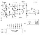
次に、図1はA/Dコンバータ5の構成を示す回路図である。この図において、40は図3に示すサンプルホールド回路31の出力信号Vampが加えられる端子であり、信号Vampは抵抗RBを介してコンパレータ41の非反転入力端へ加えられる。42は電源電圧VCCが加えられる端子であり、半導体スイッチSc4を介してコンデンサC1の一端に接続されている。43は図3に示すレファランス電圧VRが加えられる端子であり、半導体スイッチSc3を介してコンデンサC1の一端に接続されている。コンデンサC1の他端は半導体スイッチSc1を介してレファランス電圧VRが加えられる端子44に接続されると共に、半導体スイッチSc2を介して演算増幅器45の反転入力端に接続されている。
Next, FIG. 1 is a circuit diagram showing a configuration of the A /
46はリファランス電圧VSUBが加えられる端子であり、半導体スイッチSc4Sを介してコンデンサC2の一端に接続されている。47はレファランス電圧VRが加えられる端子であり、半導体スイッチSc3Sを介してコンデンサC2の一端に接続されている。コンデンサC2の他端は半導体スイッチSc1Sを介してレファランス電圧VRが加えられる端子48に接続されると共に、半導体スイッチSc2Sを介して演算増幅器45の反転入力端に接続されている。演算増幅器45の反転入力端および出力端間には、半導体スイッチSdおよびコンデンサC3が並列に接続され、非反転入力端へはレファランス電圧VRが端子49を介して加えられ、演算増幅器45の出力信号は信号Vintegとして抵抗RAを介してコンパレータ41の非反転入力端へ加えられる。ここで、スイッチSdは制御回路6(図2)から出力される信号RESによってON/OFF制御される。また、抵抗RAの抵抗値は抵抗RBと同一である。また、コンパレータ41の反転入力端へは、端子50を介してレファランス電圧VRが加えられ、コンパレータ41の出力信号CMPが端子51を介して図2の制御回路6へ出力される。なお、符号52は半導体スイッチSc1〜Sc4およびSc1S〜Sc4Sの構成を示す図であり、各スイッチSc1〜Sc4およびSc1S〜Sc4SはいずれもPチャネルFETおよびNチャネルFETを並列接続して構成されている。
46 is a terminal to which the reference voltage VSUB is applied, and is connected to one end of the capacitor C2 via the semiconductor switch Sc4S. 47 is a terminal to which the reference voltage VR is applied, and is connected to one end of the capacitor C2 via the semiconductor switch Sc3S. The other end of the capacitor C2 is connected to a terminal 48 to which a reference voltage VR is applied via a semiconductor switch Sc1S, and is connected to an inverting input terminal of the
53は上述したスイッチSc1〜Sc4およびSc1S〜Sc4SをON/OFF制御する信号CK1〜CK4、CK1S〜CK4Sを、図1の制御回路6から出力されるクロックパルスCKおよび信号FIN、UDに基づいて生成し出力するタイミング信号発生回路である。
53 generates signals CK1 to CK4 and CK1S to CK4S for ON / OFF control of the above-described switches Sc1 to Sc4 and Sc1S to Sc4S based on the clock pulse CK and signals FIN and UD output from the
図2の制御回路6は、CPU8からインターフェイス7を介して受けた指示に基づいて、前述したスイッチS1X、S3X、S1Y、S3Y、S1〜S4、S5をON/OFF制御する信号を出力し、また、クロックパルスCKおよび信号RES、FIN、UDを上述したA/Dコンバータ5へ出力する。また、クロックパルスCKを内部のカウンタによってアップカウントし、A/Dコンバータ5から出力される信号CMPを受けてカウントを停止し、カウント結果を変換後データとしてインターフェイス7を介してCPU8へ出力する(詳細は後述する)。
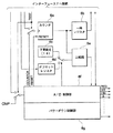
図10に、図2における制御回路6(16)の主要部の構成を示す。カウンタ6aは積分型A/Dを構成する。クロックCOUNTCKによりアップカウントし、リセット(RESET)入力を備えている。一時レジスタ6bは、カウンタ6aの値をインターフェイス7を介してCPU8が読むため一時的に保持する。下限設定6cは、A/D動作時に下限電圧を設定する。固定値16としてある。オフセットレジスタ6dは、インターフェイス7を介してCPU8が設定する。比較器6eはカウンタ6aの値と下限設定6cまたはオフセットレジスタ6dの値を比較する。A/D制御部6fは、インターフェイス7を介してCPU8からの指示により測定の開始、A/D動作の切り換え、各種タイミング信号発生を行う。パワーダウン制御部6gは省電力化のために測定動作を行っていない部分を休止状態とする。A/D制御部6fに入力される信号CMP(図1参照)、カウンタ6aのクロックCOUNTCKは、テスト時には切り換えてテスト用信号を入力する。なお、下限設定6cはこの実施形態においては固定値であるが、レジスタとしてインターフェイス7を介してCPU8から入力してもよい。
The
FIG. 10 shows a configuration of a main part of the control circuit 6 (16) in FIG. The counter 6a constitutes an integral type A / D. It is up-counted by the clock COUNTCK and has a reset (RESET) input. The
次に、図4は図2におけるZ軸センサ11、増幅部13、14の詳細を示す回路図である。この図において、11a〜11dはブリッジ接続されたGMR素子であり、これらによってZ軸センサ11が構成されている。このZ軸センサ11の電源端子は電源電圧VCCに接続され、接地端子がFET61を介して接地されている。FET61は、Z軸方向の地磁気測定の際に制御回路16から出力される信号によってONとなる。増幅器62、63は各々増幅度1のバッファ増幅器であり、Z軸センサ11の2出力を各々増幅する。R1〜R4は抵抗、64は増幅器であり、これらによってバッファ増幅器62、63の出力の差を増幅する差動増幅器が構成されている。また、端子65はレファランス電圧VRが加えられる端子である。また、66は傾斜センサ12の出力を増幅する増幅度1の増幅器であり、図2の増幅部14を構成する。そして、この増幅器66の出力端および増幅器64の出力端が共通接続されて端子68に接続され、この端子68が図2のA/Dコンバータ15に入力端に接続されている。
FIG. 4 is a circuit diagram showing details of the Z-
70はレファランス電圧発生回路であり、A/Dコンバータ15において使用されるレファランス電圧VR、VSUBを生成して出力する。すなわち、このレファランス電圧発生回路70において、R1X〜R3Xはシリーズ接続された抵抗であり、抵抗R1Xの一端が電源電圧VCCに接続され、抵抗R3Xの一端がZ軸センサ11とFET61の接続点に接続されている。71、72は増幅度1の増幅器であり、増幅器71は抵抗R1XおよびR2Xの接続点の電圧をレファランス電圧VSUBとして出力するためのバッファとして動作し、増幅器72は抵抗R2XおよびR3Xの接続点の電圧をレファランス電圧VRとして出力するためのバッファとして動作する。
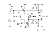
図5は図4における増幅器64、66の構成を示す回路図である。(増幅器62,63,71,72も同一の構成である。)この図において、80〜82はPチャネルFET、93は定電流回路である。FET80、81およびFET80、82はそれぞれカレントミラー接続となっており、FET81、82のソース−ドレインには各々FET80の電流と同一の(または比例する)電流が流れる。83、84はPチャネルFET、85、86はNチャネルFETであり、FET83のゲートが反転入力端innに、FET84のゲートが非反転入力端inpに各々接続されている。そして、これらのFET83〜86によって入力端inn、inpの信号の差を増幅する差動増幅回路が構成されている。87はNチャネルFETであり、上述した差動増幅回路の出力を増幅し、出力端子outへ出力する。
FIG. 5 is a circuit diagram showing the configuration of the
88はPチャネルFET、89はNチャネルFETであり、FET88のゲートには信号pdを反転した信号/pdが加えられ、FET89のゲートに信号pdが加えられる。また、FET88のソースは電源電圧VCCに接続され、ドレインがFET82のゲートに接続されている。また、FET89のソースは接地され、ドレインがFET87のゲートに接続されている。これらのFET88、89は出力端子outを能動状態とするかハイインピーダンス状態とするかを制御するもので、信号pdを”H(ハイ)”レベルにすると、FET88、89が共にONとなり、これによりFET82、87がOFFとなり、出力端子outがハイインピーダンスとなる。一方、信号pdを”L(ロー)”レベルにすると、FET88、89が共にOFFとなり、これによりFET82、87が能動状態となり、出力端子outが能動状態となる。なお、図5の信号pdは、図4での増幅器62〜64ではPDSE、増幅器66ではPDAC、増幅器71、72ではPDとして示す。
88 is a P-channel FET and 89 is an N-channel FET. A signal / pd obtained by inverting the signal pd is applied to the gate of the
図4に示す回路は、Z軸方向の地磁気測定においては、制御回路16から増幅器64、62、63へ信号PDSEとして”L”レベルの信号が加えられる一方、増幅器66へは信号PDACとして”H”レベルの信号が加えられ、増幅器71、72のPDは”L”レベルとされ、これにより増幅器64は能動状態、増幅器66はハイインピーダンス状態となる。一方、傾斜センサ12による傾斜度測定においては、制御回路16から増幅器64へ信号PDSEとして”H”レベルの信号が加えられる一方、増幅器66へは信号PDACとして”L”レベルの信号が加えられ、増幅器71、72のPDは”L”レベルとされ、これにより増幅器64はハイインピーダンス状態、増幅器66は能動状態となる。さらに、Z軸方向の地磁気測定および傾斜センサ12の傾斜測定も行わない時は、PDSE、PDAC、PDいずれも”H”レベルとされ、各増幅器は休止状態(出口はハイインピーダンス)となる。
ここではZ軸方向の地磁気測定について示したが、X軸、Y軸についても同様の切換方法ができる。その場合は、図3において、増幅器24、25、26をもう1組用意する。各増幅器を図5と同様の構成としてpd信号をX軸測定、Y軸測定に応じて制御すればよい。
In the circuit shown in FIG. 4, in the geomagnetism measurement in the Z-axis direction, an “L” level signal is applied as a signal PDSE from the
Although the geomagnetism measurement in the Z-axis direction is shown here, the same switching method can be performed for the X-axis and the Y-axis. In that case, another set of
次に、図1に示すA/Dコンバータ5(15)および制御回路6(16)の動作を図6、図7に示すタイミングチャートを参照して説明する。
このA/Dコンバータ5は(1)オフセット測定、(2)通常データ測定の2処理によってA/D変換を行う。すなわち、従来のA/Dコンバータは図8(b)に示すように、一定の細かいステップで比較電圧を最下限電圧から順次上昇させつつクロックパルスをカウントし、比較電圧が被変換電圧を超えた時のカウント値を変換データとして出力していたが、このA/Dコンバータ5は図8(a)に示すように、まず、(1)オフセット測定によって粗いステップで概略の変換データを取得し、次いで、(2)通常データ測定によって概略変換データの近傍において細かいステップで比較電圧を順次上昇させて正確な変換データを得るようになっている。以下、詳述する。
Next, operations of the A / D converter 5 (15) and the control circuit 6 (16) shown in FIG. 1 will be described with reference to timing charts shown in FIGS.
The A /
(1)オフセット測定
図6はオフセット測定の動作を示すタイミングチャートである。以下、X軸方向の地磁気の強さを測定する場合について説明する。この場合、制御回路6のA/D制御部6fは、まず、FET21(図3)をONとする信号Xを出力し、また、スイッチS1X、S3X、S1、S3、S5をONとする信号Xを出力する。次いで、クロックパルスCK、”H”レベルのリセット信号RES、”L”レベルの信号UDおよびFINをA/Dコンバータ5へ出力する(図6の時刻t1)。
(1) Offset Measurement FIG. 6 is a timing chart showing the offset measurement operation. Hereinafter, a case where the strength of geomagnetism in the X-axis direction is measured will be described. In this case, the A /
FET21がONになると、X軸センサ1に電源が供給され、GMR素子1a、1bの接続点の電圧およびGMR素子1c、1dの接続点の電圧がそれぞれ増幅器24、25の各入力端へ供給され、増幅器26からその時の地磁気のX軸方向の強さに対応する信号が出力される。そして、その信号によってサンプルホールド回路31のコンデンサ29が充電される。制御回路6は増幅器26の出力が安定した時点でスイッチS5をOFFとする。以後、増幅器30からその時の地磁気のX軸方向の強さを示す信号Vampが出力される。
When the
また、FET21がONになると、シリーズ接続された抵抗R1X、R2X、R3Xの両端に電源が供給され、抵抗R1X〜R3Xの分圧比に応じた電圧がコンデンサ38、39に充電される。そして、前記スイッチS5の場合と同様に、スイッチS1X、S3XをOFFとする。これにより、増幅器36、37からレファランス電圧VR、VSUBが出力される。
また、制御回路6からリセット信号RESとして”H”レベルの信号が出力されると、コンデンサC3(図1)の両端が短絡されてコンデンサC3が放電され、また、演算増幅器45の反転入力端および出力端間が短絡されることから、演算増幅器45の出力信号Vintegが非反転入力端の信号と同じ信号VRとなる。
When the
Further, when an “H” level signal is output from the
制御回路6は、リセット信号RES”H”を出力した後、コンデンサC3が充分に放電される時間、ここでは、クロックパルスCKの128タイミング経過した時刻t2において、図6に示すように、リセット信号RESを”L”レベルに戻す。また、カウンタ6aをリセットし、比較器6eの入力を下限設定(ここでは16)6cに切り換える。制御回路6のA/D制御部6fから信号が出力されるFIN、UDによって、タイミング制御回路53からスイッチSc1〜Sc4をON/OFF制御する信号CK1〜CK4が出力される。これにより、まず、スイッチSc1、Sc3がON、スイッチSc2、Sc4がOFFとされ(各スイッチは制御信号が”H”レベルでON、”L”レベルでOFFとする)、次いで、スイッチSc2、Sc4がON、スイッチSc1、Sc3がOFFとされ、以下、この動作がクロックパルスCKの2周期毎に繰り返される。なお、この時、スイッチSc1S〜Sc4SはいずれもOFF状態にある。そして、上述したスイッチSc1〜Sc4の動作により、コンデンサC3に一定電圧が逐次充電され、これにより、演算増幅器45の出力信号Vintegが、図6に示すように、階段状に下降する。この動作原理を以下に説明する。
The
いま、ある時刻tにおける演算増幅器45の出力信号をVinteg(t)とすると、コンデンサC3の充電電荷Q3(t)は、
Q3(t)=−C3(Vinteg(t)−VR)…(1)
となる。次に、スイッチSc1、Sc3がON、スイッチSc2、Sc4がOFFになると、コンデンサC1の両端が短絡され、また、演算増幅器45の反転入力端とコンデンサC1との間が開放されることから、コンデンサC1、C3の電荷Q1(t+1)、Q3(t+1)はそれぞれ、
Q1(t+1)=0…(2) Q3(t+1)=Q3(t)…(3)
となる。
If the output signal of the
Q3 (t) = − C3 (Vinteg (t) −VR) (1)
It becomes. Next, when the switches Sc1 and Sc3 are turned on and the switches Sc2 and Sc4 are turned off, both ends of the capacitor C1 are short-circuited, and the gap between the inverting input terminal of the
Q1 (t + 1) = 0 (2) Q3 (t + 1) = Q3 (t) (3)
It becomes.
次に、スイッチSc1、Sc3がOFF、スイッチSc2、Sc4がONになると、コンデンサC1、C3が直列接続され、コンデンサC1が電圧(VCC−VR)まで充電され、コンデンサC3もコンデンサC1と同量の電荷が充電される。すなわち、コンデンサC1に充電される電荷Q1(t+2)は、
Q1(t+2)=C1(VCCーVR)…(4)
となり、また、コンデンサC3の充電電荷Q3(t+2)は、
Q3(t+2)=Q3(t+1)+Q1(t+2)
=Q3(t)+Q1(t+2)…(5)
となる。また、Q3(t+2)については、
Q3(t+2)=−C3(Vinteg(t+2)−VR)…(6)
なる関係が成り立つ。
Next, when the switches Sc1 and Sc3 are turned off and the switches Sc2 and Sc4 are turned on, the capacitors C1 and C3 are connected in series, the capacitor C1 is charged to the voltage (VCC-VR), and the capacitor C3 has the same amount as the capacitor C1. Charge is charged. That is, the charge Q1 (t + 2) charged in the capacitor C1 is
Q1 (t + 2) = C1 (VCC-VR) (4)
In addition, the charge Q3 (t + 2) of the capacitor C3 is
Q3 (t + 2) = Q3 (t + 1) + Q1 (t + 2)
= Q3 (t) + Q1 (t + 2) (5)
It becomes. For Q3 (t + 2),
Q3 (t + 2) = − C3 (Vinteg (t + 2) −VR) (6)
The relationship becomes true.
上記(5)式に、(6)式、(1)式、(4)式を代入すれば、
−C3(Vinteg(t+2)−VR)=−C3(Vinteg(t)−VR)
+C1(VCCーVR)…(7)
なる式が得られ、この(7)式から、
Vinteg(t+2)=Vinteg(t)−(C1/C3)(VCC−VR)…(8)
なる式が得られる。
Substituting (6), (1), and (4) into (5) above,
−C3 (Vinteg (t + 2) −VR) = − C3 (Vinteg (t) −VR)
+ C1 (VCC-VR) ... (7)
From this equation (7),
Vinteg (t + 2) = Vinteg (t)-(C1 / C3) (VCC-VR) (8)
The following formula is obtained.
この(8)式から明らかなように、スイッチSc1〜Sc4が上述したON/OFF動作を繰り返すと、演算増幅器45の出力信号Vintegが、
Cstep=(VCC−VR)・C1/C3
なるステップ幅で逐次下降する。この下降が16ステップ行われた時点で、カウンタ6aの値と下限設定6cの値が一致したことを比較器6eで検出し、制御回路6が信号UDを”H”に変化させる(図6の時刻t3)。この時、信号Vintegは次の電圧となっている。
Vinteg=VR−16Cstep
これは、測定に当たっての下限の電圧値(図8(a)のMINに相当)にVintegを設定したことである。
As is apparent from the equation (8), when the switches Sc1 to Sc4 repeat the above-described ON / OFF operation, the output signal Vinteg of the
Cstep = (VCC-VR) .C1 / C3
It descends sequentially with step width. When the descending is performed for 16 steps, the
Vinteg = VR-16Cstep
This is because Vinteg is set to the lower limit voltage value (corresponding to MIN in FIG. 8A) in the measurement.
そして、信号UDが”H”に変化すると同時にカウンタ6aをリセットし、以後、タイミング信号発生回路53から出力される信号CK1〜CK4によって、スイッチSc1、Sc4がON、スイッチSc2、Sc3がOFFとされ、次いで、スイッチSc2、Sc3がON、スイッチSc1、Sc4がOFFとされ、この動作がクロックパルスCKの2周期毎に繰り返される。そして、この動作により、コンデンサC3から一定電荷が逐次放電され、これにより、演算増幅器45の出力信号Vintegが、図6に示すように、階段状に上昇する。この動作原理を以下に説明する。
At the same time as the signal UD changes to "H", the counter 6a is reset. Thereafter, the signals Sc1 to CK4 output from the timing
いま、スイッチSc2、Sc3がONなった後、OFFとなる直前の時刻tにおける演算増幅器45の出力信号をVinteg(t)とすると、コンデンサC1、C3の充電電荷Q1(t)、Q3(t)は、
Q1(t)=0…(9)
Q3(t)=−C3(Vinteg(t)−VR)…(10)
となる。次に、スイッチSc1、Sc4がON、スイッチSc2、Sc3がOFFになると、コンデンサC1が電圧(VCC−VR)によって充電され、また、演算増幅器45の反転入力端とコンデンサC1との間が開放されることから、コンデンサC1、C3の電荷Q1(t+1)、Q3(t+1)は、
Q1(t+1)=C1(VCC−VR)…(11)
Q3(t+1)=Q3(t)…(12)
となる。
Now, assuming that the output signal of the
Q1 (t) = 0 ... (9)
Q3 (t) = − C3 (Vinteg (t) −VR) (10)
It becomes. Next, when the switches Sc1 and Sc4 are turned on and the switches Sc2 and Sc3 are turned off, the capacitor C1 is charged by the voltage (VCC-VR), and the inverting input terminal of the
Q1 (t + 1) = C1 (VCC-VR) (11)
Q3 (t + 1) = Q3 (t) (12)
It becomes.
次に、スイッチSc1、Sc4がOFF、スイッチSc2、Sc3がONになると、コンデンサC1、C3が直列接続され、かつ、コンデンサC1の両端電圧が共に電圧VRとなることから、コンデンサC1の電荷を打ち消すためコンデンサC3の電荷が放電される。すなわち、この時点においてコンデンサC1、C3の電荷Q1(t+2)、Q3(t+2)はそれぞれ、
Q1(t+2)=0…(13)
Q3(t+2)=Q3(t+1)−Q1(t+1)
=Q3(t)−Q1(t+1)…(14)
となる。また、Q3(t+2)については、
Q3(t+2)=−C3(Vinteg(t+2)−VR)…(15)
なる関係が成り立つ。
Next, when the switches Sc1 and Sc4 are turned OFF and the switches Sc2 and Sc3 are turned ON, the capacitors C1 and C3 are connected in series, and the voltage across the capacitor C1 becomes the voltage VR. Therefore, the electric charge of the capacitor C3 is discharged. That is, at this time, the charges Q1 (t + 2) and Q3 (t + 2) of the capacitors C1 and C3 are respectively
Q1 (t + 2) = 0 ... (13)
Q3 (t + 2) = Q3 (t + 1) -Q1 (t + 1)
= Q3 (t) -Q1 (t + 1) (14)
It becomes. For Q3 (t + 2),
Q3 (t + 2) = − C3 (Vinteg (t + 2) −VR) (15)
The relationship becomes true.
上記(14)式に、(15)式、(10)式、(11)式を代入すれば、
−C3(Vinteg(t+2)−VR)=−C3(Vinteg(t)−VR)
−C1(VCCーVR)…(16)
なる式が得られ、この(16)式から、
Vinteg(t+2)=Vinteg(t)+(C1/C3)(VCC−VR)…(17)
なる式が得られる。
Substituting (15), (10), and (11) into (14) above,
−C3 (Vinteg (t + 2) −VR) = − C3 (Vinteg (t) −VR)
-C1 (VCC-VR) (16)
From this equation (16),
Vinteg (t + 2) = Vinteg (t) + (C1 / C3) (VCC-VR) (17)
The following formula is obtained.
この(17)式から明らかなように、時刻t3以後、信号VintegがCstep単位で逐次上昇する。またこの時、コンパレータ41の非反転入力端の信号Vaiは、抵抗RA、RBが同一の抵抗値であることから、
Vai=(Vamp+Vinteg)/2
となり、この信号Vaiも信号Vintegの上昇に伴って逐次上昇する。そして、時刻t4において、信号Vaiが電圧VRを越えると、コンパレータ41の出力信号CMPが反転し、”H”レベルとなる。制御回路6のA/D変換部6fはこの信号CMP”H”を受けて、カウンタ6aのアップカウントを停止する(COUNTCKを止める)。この時のカウンタのカウント値がオフセットデータとなり、CPU8はインターフェイス7を介して一時レジスタ6bから読み出し、内部のレジスタ(またはメモリ)にセットされる。また、CMPが”H”レベルになったことをCPU8へ通知し、CPU8が直ちに一時レジスタ6bの値を読み出すこともできる。この場合は、カウンタ6aを停止させなくてもよい。
As is apparent from the equation (17), after time t3, the signal Vinteg sequentially increases in units of Cstep. At this time, since the signal Vai at the non-inverting input terminal of the
Vai = (Vamp + Vinteg) / 2
This signal Vai also rises sequentially as the signal Vinteg rises. At time t4, when the signal Vai exceeds the voltage VR, the output signal CMP of the
(2)通常データ測定
図7に通常データ測定時のタイミングチャートを示す。通常データ測定においては、CPU8は前述のオフセット測定により得られた予め保持しているオフセットデータよりも少なめ(図8の場合は12をセット)をオフセットレジスタ6dに書き込み、比較器6eの入力をオフセットレジスタ6d側に切り換え、測定開始をA/D制御部6fに指示する。制御回路6のA/D制御部6fは、まず、クロックパルスCK、”H”レベルのリセット信号RES、”L”レベルの信号UDおよびFINをA/Dコンバータ5へ出力し(時刻t5)、次いで、時刻t6においてリセット信号RESを”L”に戻す。以後、信号Vintegがステップ幅Cstepで逐次下降する。この下降が16ステップ行われた時点で、制御回路6が信号UDを”H”に変化させる(図7の時刻t7)。この時、信号Vintegは(VR−16Cstep)となっている。そして、信号UDが”H”に変化すると、以後、演算増幅器45の出力信号Vintegが、階段状に上昇する。以上の動作は上述した図6における時刻t1〜t4の動作と同じである。
(2) Normal Data Measurement FIG. 7 shows a timing chart during normal data measurement. In the normal data measurement, the CPU 8 writes a smaller amount (set 12 in the case of FIG. 8) to the offset
制御回路6は時刻t7において信号UDを”H”とした後、カウンタ6aをリセットし、クロックパルスCKのアップカウントを行う。そして、カウンタのカウント値が上述したオフセットレジスタ6dに設定されたオフセットデータと一致した時点において、比較器6eの一致信号により信号FINを”H”とし(時刻t8)、また、カウンタをリセットし、以後、再びクロックパルスCKをアップカウントする。信号FINが”H”になると、タイミング信号発生回路53がスイッチSc1S〜Sc4SをON/OFF制御する信号CK1S〜CK4Sを出力する。これにより、まず、スイッチSc1S、Sc4SがON、スイッチSc2S、Sc3SがOFFとされ、次いで、スイッチSc2S、Sc3SがON、スイッチSc1S、Sc4SがOFFとされ、以下、この動作がクロックパルスCKの2周期毎に繰り返される。なお、この時、スイッチSc1〜Sc4はいずれもOFF状態となる。
The
スイッチSc1S〜Sc4Sが上述した動作を繰り返すと、図6における時刻t3〜t4の動作と同様の動作原理によって、信号Vintegが、
Fstep=(VSUB−VR)・C2/C3
なるステップ幅で逐次上昇する。ここで、コンデンサC2の容量はコンデンサC1の容量よりはるかに小さい容量が選ばれており、また、電圧VSUBも電圧VCCより小さい電圧である。この結果、ステップ幅Fstepはステップ幅Cstepよりはるかに小さくなり、信号Vintegは時刻t7〜t8の間よりはるかに小さいステップで上昇する。
When the switches Sc1S to Sc4S repeat the above-described operation, the signal Vinteg is expressed by the same operation principle as that at the times t3 to t4 in FIG.
Fstep = (VSUB−VR) · C2 / C3
Ascending step by step width. Here, the capacitance of the capacitor C2 is selected to be much smaller than the capacitance of the capacitor C1, and the voltage VSUB is also smaller than the voltage VCC. As a result, the step width Fstep is much smaller than the step width Cstep, and the signal Vinteg rises in steps much smaller than those between times t7 and t8.
そして、信号Vai=(Vinteg+Vamp)/2が電圧VRを越えると(時刻t9)、コンパレータ41の出力信号CMPが”H”に反転する。制御回路6はこの”H”信号を受け、カウンタ6aのカウントを停止する。CPU8はインターフェイス7を介して一時レジスタ6bの値を読み出す。これが図8(a)でのNORMAL MEASUREMENTの測定値となる。また、CMPが”H”になったことをCPU8へ通知し、CPU8が直ちに一時レジスタ6bの値を読み出すこともできる。この場合はカウンタ6aを停止させなくてもよい。
When the signal Vai = (Vinteg + Vamp) / 2 exceeds the voltage VR (time t9), the output signal CMP of the
以上詳述したように、上記実施形態によれば、(1)オフセット測定において概略の変換データを取得し、次いで(2)通常データ測定において正確な変換データを得るようになっている。これにより、この実施形態では、測定時間は最大でも約1310クロックで済む。一方、従来の方式(図9参照)によれば、最大で8192クロック必要である。したがって、この実施形態によれば、従来の約1/6の時間でA/D変換することができる。
また、通常の動作状態では、オフセット値はほとんど変化しないはずである。したがって、オフセット測定(図6)は測定毎に行う必要がない。通常は、通常データ測定(図7)のみを行えばよいので、大きく測定時間を短縮することができる。オフセット測定は、機器の動作開始時や、外部磁界の影響等でオフセット値が狂ってしまった時に必要に応じて行えばよい。
なお、上記実施形態において、サンプルホールド回路31を設けず、増幅器26の出力を直接A/Dコンバータ5に入力してもよい。
また、上記実施形態は、信号Vintegを上昇させて変換データの測定を行っているが、逆に、信号Vintegを下降させて測定を行なってもよい。
As described above in detail, according to the above-described embodiment, (1) rough conversion data is obtained in offset measurement, and (2) accurate conversion data is obtained in normal data measurement. As a result, in this embodiment, the maximum measurement time is about 1310 clocks. On the other hand, according to the conventional system (see FIG. 9), 8192 clocks are required at the maximum. Therefore, according to this embodiment, A / D conversion can be performed in about 1/6 of the conventional time.
In the normal operation state, the offset value should hardly change. Therefore, the offset measurement (FIG. 6) need not be performed for each measurement. Usually, only normal data measurement (FIG. 7) needs to be performed, so that the measurement time can be greatly shortened. The offset measurement may be performed as necessary when the operation of the device starts or when the offset value has changed due to the influence of an external magnetic field or the like.
In the above embodiment, the output of the
In the above embodiment, the conversion data is measured by increasing the signal Vinteg. Conversely, the measurement may be performed by decreasing the signal Vinteg.
この発明は、携帯端末に内蔵される地磁気測定回路等に用いられる。 The present invention is used for a geomagnetism measuring circuit or the like built in a portable terminal.
1…X軸センサ、2…Y軸センサ、3…切換手段、4…増幅部、5…A/Dコンバータ、6…制御回路、7…インターフェイス、8…CPU、11…Z軸センサ、12…傾斜センサ、13、14…増幅部、15…A/Dコンバータ、16…制御回路、17…インターフェイス、1a〜1d、2a〜2d、11a〜11d…GMR素子、24〜26、30…増幅器、29、C1〜C3…コンデンサ、31…サンプルホールド回路、41…コンパレータ、45…演算増幅器、53…タイミング信号発生回路、S1〜S5、Sc1〜Sc4、Sc1S〜Sc4S…スイッチ、
DESCRIPTION OF
Claims (3)
前記磁気センサの出力を増幅する増幅手段と、
所定のクロック数に対応する第1期間に、クロックパルスに同期して第1のステップ幅で単調増加する電圧を発生させ、その後の第2期間に、クロックパルスに同期して前記第1のステップ幅より小さい第2のステップ幅で前記第1期間終了時の電圧から単調増加する電圧を発生させる電圧発生手段と、
前記第2期間の開始から、前記電圧発生手段の発生電圧値と前記増幅手段の出力電圧値とを所定の比率で加算した電圧値が閾値電圧値以上となるまで、クロックパルスをカウントし、カウント結果を前記磁気の強さを表すデータとして出力するカウント手段と、
を具備することを特徴とする磁気測定回路。 A magnetic sensor for measuring the strength of the magnetism;
Amplifying means for amplifying the output of the magnetic sensor;
In the first period corresponding to a predetermined number of clocks, a voltage that monotonously increases with a first step width is generated in synchronization with the clock pulse, and in the subsequent second period, the first step is synchronized with the clock pulse. Voltage generating means for generating a monotonically increasing voltage from the voltage at the end of the first period with a second step width smaller than the width;
From the start of the second period, the clock pulse is counted until the voltage value obtained by adding the voltage value generated by the voltage generating means and the output voltage value of the amplifying means at a predetermined ratio becomes equal to or higher than the threshold voltage value. Counting means for outputting the result as data representing the magnetic strength;
A magnetic measurement circuit comprising:
Priority Applications (1)
| Application Number | Priority Date | Filing Date | Title |
|---|---|---|---|
| JP2004286891A JP4496907B2 (en) | 2004-09-30 | 2004-09-30 | Magnetic measurement circuit |
Applications Claiming Priority (1)
| Application Number | Priority Date | Filing Date | Title |
|---|---|---|---|
| JP2004286891A JP4496907B2 (en) | 2004-09-30 | 2004-09-30 | Magnetic measurement circuit |
Publications (2)
| Publication Number | Publication Date |
|---|---|
| JP2006098304A JP2006098304A (en) | 2006-04-13 |
| JP4496907B2 true JP4496907B2 (en) | 2010-07-07 |
Family
ID=36238255
Family Applications (1)
| Application Number | Title | Priority Date | Filing Date |
|---|---|---|---|
| JP2004286891A Expired - Fee Related JP4496907B2 (en) | 2004-09-30 | 2004-09-30 | Magnetic measurement circuit |
Country Status (1)
| Country | Link |
|---|---|
| JP (1) | JP4496907B2 (en) |
Families Citing this family (1)
| Publication number | Priority date | Publication date | Assignee | Title |
|---|---|---|---|---|
| WO2009101548A1 (en) * | 2008-02-12 | 2009-08-20 | Nxp B.V. | Signal conditioning circuit for magnetoresistive sensors |
Citations (2)
| Publication number | Priority date | Publication date | Assignee | Title |
|---|---|---|---|---|
| JP2003121520A (en) * | 2001-10-18 | 2003-04-23 | Yamaha Corp | Magnetism detecting circuit and azimuth detecting circuit |
| WO2003081182A1 (en) * | 2002-03-22 | 2003-10-02 | Asahi Kasei Emd Corporation | Angle determining apparatus and angle determining system |
Family Cites Families (4)
| Publication number | Priority date | Publication date | Assignee | Title |
|---|---|---|---|---|
| JPS6010914A (en) * | 1983-06-30 | 1985-01-21 | Shimadzu Corp | Automatic zero circuit |
| ATE86800T1 (en) * | 1988-04-21 | 1993-03-15 | Landis & Gyr Betriebs Ag | INTEGRATED SEMICONDUCTOR CIRCUIT WITH A MAGNETIC SENSOR MADE OF SEMICONDUCTOR MATERIAL. |
| JPH03237899A (en) * | 1990-02-15 | 1991-10-23 | Yamaha Corp | Howling suppression device |
| JP3326933B2 (en) * | 1993-12-24 | 2002-09-24 | 株式会社デンソー | Sensor signal processing device |
-
2004
- 2004-09-30 JP JP2004286891A patent/JP4496907B2/en not_active Expired - Fee Related
Patent Citations (2)
| Publication number | Priority date | Publication date | Assignee | Title |
|---|---|---|---|---|
| JP2003121520A (en) * | 2001-10-18 | 2003-04-23 | Yamaha Corp | Magnetism detecting circuit and azimuth detecting circuit |
| WO2003081182A1 (en) * | 2002-03-22 | 2003-10-02 | Asahi Kasei Emd Corporation | Angle determining apparatus and angle determining system |
Also Published As
| Publication number | Publication date |
|---|---|
| JP2006098304A (en) | 2006-04-13 |
Similar Documents
| Publication | Publication Date | Title |
|---|---|---|
| US7652472B2 (en) | Magnetic sensor signal detection circuit using a counter | |
| US7454967B2 (en) | Signal conditioning methods and circuits for a capacitive sensing integrated tire pressure sensor | |
| US7355398B2 (en) | Exciting coil drive circuit of magnetic sensor | |
| US7898268B2 (en) | Circuit and method for capacitor effective series resistance measurement | |
| US20060273804A1 (en) | Capacitive measuring sensor and associated ,measurement method | |
| EP1158789B1 (en) | Photodetector device | |
| US10067156B2 (en) | Physical quantity sensor, sensor unit, electronic apparatus, moving object, and physical quantity detection method | |
| US20110133723A1 (en) | Sensor Arrangement and Method for Operating a Sensor Arrangement | |
| US8613222B2 (en) | Detector, physical quantity measuring device, and electronic apparatus | |
| US9110113B2 (en) | Method of measuring a physical parameter and electronic interface circuit for a capacitive sensor for implementing the same | |
| JP2007101317A (en) | Voltage measuring method and voltage measuring instrument | |
| JP4496907B2 (en) | Magnetic measurement circuit | |
| JP2004340782A (en) | Magnetic field sensor | |
| US20110062941A1 (en) | Detector, physical quantity measuring device, and electronic apparatus | |
| JP2006098306A (en) | Magnetic measuring apparatus | |
| JP2002107256A (en) | Pressure sensor circuit | |
| JP2006098307A (en) | Magnetic measuring apparatus | |
| JP2006098308A (en) | Magnetometric device | |
| JP5082952B2 (en) | Coulomb counter and dynamic range adjustment method | |
| JP2006098305A (en) | Magnetic measuring apparatus | |
| KR101620590B1 (en) | Muti-mode capacitance to digital converter and resistance to digital converter circuit | |
| JP2004340673A (en) | Signal processing circuit and dynamic amount sensor | |
| JP2009229165A (en) | Coulomb counter, and its internal power supply control method | |
| JP3178930B2 (en) | Double integral type A / D converter | |
| JP2001099875A (en) | Analog input detection circuit and voltage detection level judging method |
Legal Events
| Date | Code | Title | Description |
|---|---|---|---|
| A621 | Written request for application examination |
Free format text: JAPANESE INTERMEDIATE CODE: A621 Effective date: 20070720 |
|
| A131 | Notification of reasons for refusal |
Free format text: JAPANESE INTERMEDIATE CODE: A131 Effective date: 20091215 |
|
| A521 | Request for written amendment filed |
Free format text: JAPANESE INTERMEDIATE CODE: A523 Effective date: 20100215 |
|
| TRDD | Decision of grant or rejection written | ||
| A01 | Written decision to grant a patent or to grant a registration (utility model) |
Free format text: JAPANESE INTERMEDIATE CODE: A01 Effective date: 20100323 |
|
| A01 | Written decision to grant a patent or to grant a registration (utility model) |
Free format text: JAPANESE INTERMEDIATE CODE: A01 |
|
| A61 | First payment of annual fees (during grant procedure) |
Free format text: JAPANESE INTERMEDIATE CODE: A61 Effective date: 20100405 |
|
| FPAY | Renewal fee payment (event date is renewal date of database) |
Free format text: PAYMENT UNTIL: 20130423 Year of fee payment: 3 |
|
| R150 | Certificate of patent or registration of utility model |
Ref document number: 4496907 Country of ref document: JP Free format text: JAPANESE INTERMEDIATE CODE: R150 Free format text: JAPANESE INTERMEDIATE CODE: R150 |
|
| FPAY | Renewal fee payment (event date is renewal date of database) |
Free format text: PAYMENT UNTIL: 20140423 Year of fee payment: 4 |
|
| LAPS | Cancellation because of no payment of annual fees |