JP4475785B2 - Manufacturing method of resin-encapsulated semiconductor device - Google Patents
Manufacturing method of resin-encapsulated semiconductor device Download PDFInfo
- Publication number
- JP4475785B2 JP4475785B2 JP2000292331A JP2000292331A JP4475785B2 JP 4475785 B2 JP4475785 B2 JP 4475785B2 JP 2000292331 A JP2000292331 A JP 2000292331A JP 2000292331 A JP2000292331 A JP 2000292331A JP 4475785 B2 JP4475785 B2 JP 4475785B2
- Authority
- JP
- Japan
- Prior art keywords
- semiconductor element
- lead frame
- lead
- semiconductor device
- resin
- Prior art date
- Legal status (The legal status is an assumption and is not a legal conclusion. Google has not performed a legal analysis and makes no representation as to the accuracy of the status listed.)
- Expired - Lifetime
Links
Images


Classifications
-
- H—ELECTRICITY
- H01—ELECTRIC ELEMENTS
- H01L—SEMICONDUCTOR DEVICES NOT COVERED BY CLASS H10
- H01L2224/00—Indexing scheme for arrangements for connecting or disconnecting semiconductor or solid-state bodies and methods related thereto as covered by H01L24/00
- H01L2224/01—Means for bonding being attached to, or being formed on, the surface to be connected, e.g. chip-to-package, die-attach, "first-level" interconnects; Manufacturing methods related thereto
- H01L2224/42—Wire connectors; Manufacturing methods related thereto
- H01L2224/44—Structure, shape, material or disposition of the wire connectors prior to the connecting process
- H01L2224/45—Structure, shape, material or disposition of the wire connectors prior to the connecting process of an individual wire connector
- H01L2224/45001—Core members of the connector
- H01L2224/45099—Material
- H01L2224/451—Material with a principal constituent of the material being a metal or a metalloid, e.g. boron (B), silicon (Si), germanium (Ge), arsenic (As), antimony (Sb), tellurium (Te) and polonium (Po), and alloys thereof
- H01L2224/45138—Material with a principal constituent of the material being a metal or a metalloid, e.g. boron (B), silicon (Si), germanium (Ge), arsenic (As), antimony (Sb), tellurium (Te) and polonium (Po), and alloys thereof the principal constituent melting at a temperature of greater than or equal to 950°C and less than 1550°C
- H01L2224/45144—Gold (Au) as principal constituent
-
- H—ELECTRICITY
- H01—ELECTRIC ELEMENTS
- H01L—SEMICONDUCTOR DEVICES NOT COVERED BY CLASS H10
- H01L2224/00—Indexing scheme for arrangements for connecting or disconnecting semiconductor or solid-state bodies and methods related thereto as covered by H01L24/00
- H01L2224/01—Means for bonding being attached to, or being formed on, the surface to be connected, e.g. chip-to-package, die-attach, "first-level" interconnects; Manufacturing methods related thereto
- H01L2224/42—Wire connectors; Manufacturing methods related thereto
- H01L2224/47—Structure, shape, material or disposition of the wire connectors after the connecting process
- H01L2224/48—Structure, shape, material or disposition of the wire connectors after the connecting process of an individual wire connector
- H01L2224/4805—Shape
- H01L2224/4809—Loop shape
- H01L2224/48091—Arched
-
- H—ELECTRICITY
- H01—ELECTRIC ELEMENTS
- H01L—SEMICONDUCTOR DEVICES NOT COVERED BY CLASS H10
- H01L2224/00—Indexing scheme for arrangements for connecting or disconnecting semiconductor or solid-state bodies and methods related thereto as covered by H01L24/00
- H01L2224/01—Means for bonding being attached to, or being formed on, the surface to be connected, e.g. chip-to-package, die-attach, "first-level" interconnects; Manufacturing methods related thereto
- H01L2224/42—Wire connectors; Manufacturing methods related thereto
- H01L2224/47—Structure, shape, material or disposition of the wire connectors after the connecting process
- H01L2224/48—Structure, shape, material or disposition of the wire connectors after the connecting process of an individual wire connector
- H01L2224/481—Disposition
- H01L2224/48151—Connecting between a semiconductor or solid-state body and an item not being a semiconductor or solid-state body, e.g. chip-to-substrate, chip-to-passive
- H01L2224/48221—Connecting between a semiconductor or solid-state body and an item not being a semiconductor or solid-state body, e.g. chip-to-substrate, chip-to-passive the body and the item being stacked
- H01L2224/48245—Connecting between a semiconductor or solid-state body and an item not being a semiconductor or solid-state body, e.g. chip-to-substrate, chip-to-passive the body and the item being stacked the item being metallic
- H01L2224/48247—Connecting between a semiconductor or solid-state body and an item not being a semiconductor or solid-state body, e.g. chip-to-substrate, chip-to-passive the body and the item being stacked the item being metallic connecting the wire to a bond pad of the item
-
- H—ELECTRICITY
- H01—ELECTRIC ELEMENTS
- H01L—SEMICONDUCTOR DEVICES NOT COVERED BY CLASS H10
- H01L2224/00—Indexing scheme for arrangements for connecting or disconnecting semiconductor or solid-state bodies and methods related thereto as covered by H01L24/00
- H01L2224/01—Means for bonding being attached to, or being formed on, the surface to be connected, e.g. chip-to-package, die-attach, "first-level" interconnects; Manufacturing methods related thereto
- H01L2224/42—Wire connectors; Manufacturing methods related thereto
- H01L2224/47—Structure, shape, material or disposition of the wire connectors after the connecting process
- H01L2224/49—Structure, shape, material or disposition of the wire connectors after the connecting process of a plurality of wire connectors
- H01L2224/491—Disposition
- H01L2224/4912—Layout
- H01L2224/49171—Fan-out arrangements
Abstract
Description
【0001】
【発明の属する技術分野】
本発明は、リードフレーム上に半導体素子を搭載し、その外囲、特に半導体素子の上面側をモールド樹脂で封止した樹脂封止型半導体装置の技術分野に属するものである。
【0002】
【従来の技術】
近年、基板実装の高密度化に伴い、基板実装される半導体製品の小型化・薄型化が要求されている。LSIも、高集積化によるチップ数の削減とパッケージの小型・軽量化が厳しく要求され、いわゆるCSP(Chip Size Package)の普及が急速に進んでいる。特に、リードフレームを用いた薄型の半導体製品の開発においては、リードフレームに半導体素子を搭載し、その搭載面をモールド樹脂で封止する片面封止タイプの樹脂封止型半導体装置が開発されている。
【0003】
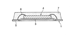
図1は樹脂封止型半導体装置の一例を示す断面図、図2はその封止樹脂を透視した状態で示す平面図である。これらの図に示される樹脂封止型半導体装置は、リードフレーム1の吊りリード2で支持されたダイパッド3に搭載された半導体素子4と、この半導体素子4の上面の電極とリードフレーム1の端子部5とを電気的に接続したワイヤー6と、半導体素子4の上側とダイパッド3の下側とを含む半導体素子4の外囲領域を封止した封止樹脂7とを備えている。この樹脂封止型半導体装置は、いわゆるアウターリードが突き出ておらず、インナーリードとアウターリードの両者が端子部5として一体となったノンリードタイプである。また、ここで用いられているリードフレーム1は、ダイパッド3が端子部5より上方に位置するように、吊りリード2がアップセット処理されている。このようにダイパッド3に段差を設けることにより、ダイパッド3の下側にも封止樹脂7を存在させている。
【0004】
上記のようなノンリードタイプの樹脂封止型半導体装置は、半導体素子のサイズが小型であるため、1枚のフレームの幅方向に複数列配列して製造するマトリックスタイプが主流である。そして、最近では、コストダウンの要求から、図3に示すような個別にモールドするタイプから、図4に示すような一括してモールドするタイプへ移行することが考えられている。
【0005】
個別モールドタイプは、図3(A)に示すように、1枚のフレームF内に小さなサイズの個々のモールドキャビティCを分かれた状態で設けるようにし、モールド後は抜型により個別に打ち抜いて図3(B)に示す半導体装置Sを得るものである。すなわち、半導体素子を銀ペースト等によりリードフレームのダイパッド上に搭載し、ワイヤーボンディングを実施した後、個々の半導体素子を個別にモールドしてから、抜型により個々の半導体装置として打ち抜くのである。
【0006】
一括モールドタイプは、図4(A)に示すように、1枚のフレームF内に大きなサイズの幾つかのモールドキャビティCを設けるようにし、その一つ一つのモールドキャビティC内には多数の半導体素子をマトリックス状に配列し、それらの半導体素子を一括してモールドした後、各リードフレームのグリッドリードLのところをダイシングソーで切断して図4(B)に示す半導体装置Sを得るものである。すなわち、半導体素子を銀ペースト等によりリードフレームのダイパッド上に搭載し、ワイヤーボンディングを実施した後、複数個配列されている半導体素子を所定のキャビティサイズで一括モールドしてから、ダイシングにより個片化するのである。
【0007】
【発明が解決しようとする課題】
一般に半導体装置では、その製造工程にて行うワイヤーボンディングを容易にするため、あらかじめリードフレームにおける端子部のワイヤー接続部分に銀メッキを施している。このメッキエリアについては、アウターリードが突き出たタイプの樹脂封止型半導体装置では、インナーリードの先端より0.3mmからダムバーの内側までという規格が多く、目視により容易にエリア合否の判定ができていた。これに対し、従来の技術で述べた如きノンリードタイプの樹脂封止型半導体装置の場合、メッキエリアが狭いため、抜き取りによる実測値でエリア精度を保証している。このため、寸法測定にかかる人件費がコストアップの要因となっていた。
【0008】
本発明は、このような問題点に鑑みてなされたものであり、その目的とするところは、ワイヤーボンディングのためのメッキエリアの精度を目視で容易に確認できるようにし、検査コストの低減を図ったノンリードタイプの樹脂封止型半導体装置の製造方法を提供することにある。
【0010】
【課題を解決するための手段】
上記の目的を達成するため、本発明の樹脂封止型半導体装置の製造方法は、リードフレームの吊りリードで支持されたダイパッド上に搭載された半導体素子と、この半導体素子の上面の電極とリードフレームの複数の端子部における銀メッキ部分とを電気的に接続したワイヤーと、端子部の下面と側面とを露出させた状態で、ワイヤーを含む半導体素子の外囲領域を封止してなる封止樹脂とを備えたノンリードタイプの樹脂封止型半導体装置を製造する方法であって、リードフレームの各端子部の内側から所定距離をおいた所に、外側の線が最大エリアとなり内側の線が最小エリアとなるようにワイヤー接続用の銀メッキエリアを規定する溝を設けておき、銀メッキを施した後の検査で銀メッキの端が溝の中にあることを確認してから、吊りリードに支持されたダイパッドの上に半導体素子を搭載し、半導体素子の上面の電極とリードフレームの複数の端子部における銀メッキ部分との間にワイヤーボンディングを実施した後、個々の半導体素子を個別にモールドしてから、抜型により個々の半導体装置に打ち抜くことを特徴としている。
【0011】
また、本発明の樹脂封止型半導体装置の製造方法は、リードフレームの吊りリードで支持されたダイパッド上に搭載された半導体素子と、この半導体素子の上面の電極とリードフレームの複数の端子部における銀メッキ部分とを電気的に接続したワイヤーと、端子部の下面と側面とを露出させた状態で、ワイヤーを含む半導体素子の外囲領域を封止してなる封止樹脂とを備えたノンリードタイプの樹脂封止型半導体装置を製造する方法であって、リードフレームの各端子部の内側から所定距離をおいた所に、外側の線が最大エリアとなり内側の線が最小エリアとなるようにワイヤー接続用の銀メッキエリアを規定する溝を設けておき、銀メッキを施した後の検査で銀メッキの端が溝の中にあることを確認してから、吊りリードに支持されたダイパッドの上に半導体素子を搭載し、半導体素子の上面の電極とリードフレームの複数の端子部における銀メッキ部分との間にワイヤーボンディングを実施した後、複数個配列されている半導体素子を所定のキャビティサイズで一括モールドしてから、ダイシングにより個片化することを特徴としている。
【0013】
【発明の実施の形態】
次に、本発明の実施の形態を図面を参照して説明する。
【0014】
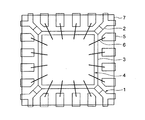
図5は本発明の樹脂封止型半導体装置の製造方法で使用するリードフレームの一例を示すもので、図5(A)は平面図、図5(B)は図5(A)のX−X断面図である。
【0015】
図示のように、リードフレーム1は、周辺部からの4本の吊りリード2でダイパッド3を支持し、そのダイパッド3に向けて周囲4辺からそれぞれ4本ずつ端子部5が突き出た状態になっている。そして、各端子部5の内側から所定距離をおいた所に表側からのハーフエッチングにより溝8が形成されている。また、図示のリードフレーム1では、ダイパッド3の裏面がハーフエッチングされて薄くなっている。このリードフレーム1は、殆どの場合、厚みが0.2mmの銅製の金属板で構成されており、溝8を形成するハーフエッチングは0.1mm程度で実施できる。また、ダイパッド裏面のハーフエッチングも0.1mm程度で実施できる。通常、このようなリードフレームが、図3(A)の如く1枚のフレームに複数個並んだ状態で配列される。
【0016】
リードフレーム1の端子部5にはワイヤー接続用の銀メッキが施されるが、端子部5に形成した溝8は、その銀メッキのエリアを規定するのに利用される。すなわち、溝8の外側の線aが最大エリア、内側の線bが最小エリアであり、検査時に銀メッキの端が溝8の中にあれば合格となる。この検査は目視により容易に行うことができる。なお、メッキエリアは端子部5の先端から0.3〜0.6mm程度であり、溝8の幅は0.12mm程度である。
【0017】
この銀メッキ済みのリードフレーム1を用いて樹脂封止型半導体装置を製造する手順は次のようである。まず、リードフレーム1における吊りリード2に支持されたダイパッド3の上に半導体素子を銀ペーストにより搭載し、半導体素子の上面の電極と端子部5の銀メッキ部分との間に金線によるワイヤーボンディングを実施した後、モールド型にセットして個別にモールドしてから、抜型により個々の半導体装置に打ち抜く。
【0018】
このようにして製造された樹脂封止型半導体装置の断面図を図6に示す。端子部5には銀メッキのエリアを規定する溝8があり、この溝8には封止樹脂7が入り込むので、端子部5と封止樹脂7との密着性を増す効果もある。なお、この樹脂封止型半導体装置は、図示の如く半導体素子4の裏側が封止樹脂7で覆われた状態になっているので、基板に実装した際に、ダイパッド3の下の基板内配線との間でデンドライトが発生するのが防止される。また、ダイパッド3が封止樹脂7から剥がれるようなことがない。
【0019】
なお、上記の説明では、個別モールドタイプについて述べたが、一括モールドタイプの樹脂封止型半導体装置についても同様である。
【0020】
【発明の効果】
以上説明したように、本発明の樹脂封止型半導体装置の製造方法は、リードフレームの吊りリードで支持されたダイパッド上に搭載された半導体素子と、この半導体素子の上面の電極とリードフレームの複数の端子部における銀メッキ部分とを電気的に接続したワイヤーと、端子部の下面と側面とを露出させた状態で、ワイヤーを含む半導体素子の外囲領域を封止してなる封止樹脂とを備えたノンリードタイプの樹脂封止型半導体装置を製造する方法であって、リードフレームの各端子部の内側から所定距離をおいた所に、外側の線が最大エリアとなり内側の線が最小エリアとなるようにワイヤー接続用の銀メッキエリアを規定する溝を設けておき、銀メッキを施した後の検査で銀メッキの端が溝の中にあることを確認してから、吊りリードに支持されたダイパッドの上に半導体素子を搭載し、半導体素子の上面の電極とリードフレームの複数の端子部における銀メッキ部分との間にワイヤーボンディングを実施した後、個々の半導体素子を個別にモールドしてから、抜型により個々の半導体装置に打ち抜くようにするか、或いは、複数個配列されている半導体素子を所定のキャビティサイズで一括モールドしてから、ダイシングにより個片化するようにしたので、目視で容易にメッキエリアの精度を確認することができ、検査コストを抑えることができる。
【図面の簡単な説明】
【図1】 樹脂封止型半導体装置の一例を示す断面図である。
【図2】 図1に示す樹脂封止型半導体装置の平面図である。
【図3】 個別モールドタイプの説明図である。
【図4】 一括モールドタイプの説明図である。
【図5】 本発明の樹脂封止型半導体装置を製造するのに使用するリードフレームの一例を示すもので、(A)は平面図、(B)は(A)のX−X断面図である。
【図6】 図5に示すリードフレームを使用して製造された樹脂封止型半導体装置を示す断面図である。
【符号の説明】
1 リードフレーム
2 吊りリード
3 ダイパッド
4 半導体素子
5 端子部
6 金属細線
7 封止樹脂
8 溝
C モールドキャビティ
F フレーム
L グリッドリード[0001]
BACKGROUND OF THE INVENTION
The present invention belongs to the technical field of a resin-encapsulated semiconductor device in which a semiconductor element is mounted on a lead frame and its outer periphery, in particular, the upper surface side of the semiconductor element is sealed with a mold resin.
[0002]
[Prior art]
In recent years, with the increase in the density of board mounting, there has been a demand for downsizing and thinning of semiconductor products mounted on the board. LSIs are also required to reduce the number of chips due to high integration and to reduce the size and weight of packages, and so-called CSP (Chip Size Package) is rapidly spreading. In particular, in the development of thin semiconductor products using lead frames, a single-side sealed type resin-sealed semiconductor device has been developed in which a semiconductor element is mounted on a lead frame and the mounting surface is sealed with a mold resin. Yes.
[0003]
FIG. 1 is a cross-sectional view showing an example of a resin-encapsulated semiconductor device, and FIG. 2 is a plan view showing the encapsulating resin as seen through. The resin-encapsulated semiconductor device shown in these drawings includes a
[0004]
Since the non-lead type resin-encapsulated semiconductor device as described above has a small semiconductor element size, a matrix type manufactured by arranging a plurality of rows in the width direction of one frame is mainly used. Recently, it has been considered to shift from the individual molding type as shown in FIG. 3 to the batch molding type as shown in FIG.
[0005]
Individual mold type, as shown in FIG. 3 (A), as provided in a state of separated individual mold cavity C of a smaller size within one frame F, after the mold is punched out individually by disconnect-type drawing The semiconductor device S shown in 3 (B) is obtained. That is, a semiconductor element is mounted on a die pad of a lead frame with silver paste or the like, after carrying out wire bonding, it is from the mold individually individual semiconductor elements, the punching as individual semiconductor devices by disconnect type.
[0006]
In the collective mold type, as shown in FIG. 4A, several mold cavities C having a large size are provided in one frame F, and each of the mold cavities C has a large number of semiconductors. The elements are arranged in a matrix, the semiconductor elements are molded together, and the grid leads L of each lead frame are cut with a dicing saw to obtain the semiconductor device S shown in FIG. is there. In other words, a semiconductor element is mounted on a die pad of a lead frame with silver paste or the like, and after wire bonding, a plurality of arrayed semiconductor elements are collectively molded with a predetermined cavity size and then separated by dicing. To do.
[0007]
[Problems to be solved by the invention]
In general, in a semiconductor device, in order to facilitate wire bonding performed in the manufacturing process, silver plating is applied in advance to a wire connection portion of a terminal portion in a lead frame. With regard to this plating area, in resin-sealed semiconductor devices of the type in which the outer lead protrudes, there are many standards ranging from 0.3 mm to the inside of the dam bar from the tip of the inner lead, and it is possible to easily determine whether the area is acceptable or not by visual inspection. It was. On the other hand, in the case of a non-lead type resin-encapsulated semiconductor device as described in the prior art, since the plating area is narrow, the area accuracy is guaranteed by an actual measurement value obtained by sampling. For this reason, the labor cost for the dimension measurement has been a cause of the cost increase.
[0008]
The present invention has been made in view of such problems, and the object of the present invention is to make it easy to visually confirm the accuracy of the plating area for wire bonding, thereby reducing the inspection cost. Another object of the present invention is to provide a method for manufacturing a non-lead type resin-encapsulated semiconductor device.
[0010]
[Means for Solving the Problems]
In order to achieve the above object, a method for manufacturing a resin-encapsulated semiconductor device of the present invention includes a semiconductor element mounted on a die pad supported by a suspension lead of a lead frame, an electrode on the upper surface of the semiconductor element, and a lead A seal formed by sealing an outer region of a semiconductor element including a wire with a wire electrically connected to silver-plated portions of a plurality of terminal portions of the frame and a lower surface and side surfaces of the terminal portion exposed. A non-lead type resin-encapsulated semiconductor device having a stop resin , wherein the outer wire becomes the maximum area at a predetermined distance from the inner side of each terminal portion of the lead frame, and the inner side A groove that defines the silver plating area for wire connection is provided so that the wire is the minimum area, and after confirming that the end of silver plating is in the groove by inspection after silver plating , Hanging A semiconductor element is mounted on a die pad supported by a card, wire bonding is performed between the electrode on the upper surface of the semiconductor element and the silver-plated portions of the plurality of terminal portions of the lead frame. after molded separately, it is characterized by punching into individual semiconductor devices by cutting die.
[0011]
The method for manufacturing a resin-encapsulated semiconductor device according to the present invention includes a semiconductor element mounted on a die pad supported by a suspension lead of a lead frame, an electrode on the upper surface of the semiconductor element, and a plurality of terminal portions of the lead frame. A wire electrically connected to the silver-plated portion, and a sealing resin formed by sealing the outer region of the semiconductor element including the wire in a state where the lower surface and the side surface of the terminal portion are exposed. A method of manufacturing a non-lead type resin-encapsulated semiconductor device, wherein the outer line is the maximum area and the inner line is the minimum area at a predetermined distance from the inner side of each terminal portion of the lead frame. As shown in the figure, a groove defining the silver plating area for wire connection was prepared, and after checking that the end of the silver plating was in the groove in the inspection after the silver plating was applied, it was supported by the suspension lead Da A semiconductor element is mounted on the pad, and after wire bonding is performed between the electrode on the upper surface of the semiconductor element and the silver-plated portions of the plurality of terminal portions of the lead frame, a plurality of semiconductor elements arranged in a predetermined manner are arranged. from collectively molded with the cavity size, it is characterized by pieces by dicing.
[0013]
DETAILED DESCRIPTION OF THE INVENTION
Next, embodiments of the present invention will be described with reference to the drawings.
[0014]
FIG. 5 shows an example of a lead frame used in the method for manufacturing a resin-encapsulated semiconductor device of the present invention. FIG. 5 (A) is a plan view, and FIG. 5 (B) is an X-axis of FIG. 5 (A). It is X sectional drawing.
[0015]
As shown in the drawing, the lead frame 1 supports the
[0016]
The
[0017]
The procedure for manufacturing a resin-encapsulated semiconductor device using the silver-plated lead frame 1 is as follows. First, a semiconductor element is mounted on the
[0018]
A cross-sectional view of the resin-encapsulated semiconductor device manufactured in this way is shown in FIG. The
[0019]
In the above description, the individual mold type has been described, but the same applies to a batch mold type resin-encapsulated semiconductor device.
[0020]
【The invention's effect】
As described above, the method for manufacturing a resin-encapsulated semiconductor device according to the present invention includes a semiconductor element mounted on a die pad supported by a suspension lead of a lead frame, an electrode on the upper surface of the semiconductor element, and a lead frame. A sealing resin formed by sealing a surrounding region of a semiconductor element including a wire with a wire electrically connecting silver-plated portions in a plurality of terminal portions and a lower surface and side surfaces of the terminal portions exposed. A non-lead type resin-encapsulated semiconductor device having a structure in which the outer line becomes the largest area at a predetermined distance from the inner side of each terminal portion of the lead frame, and the inner line is It may be provided with grooves for defining a silver plating Kie rear wire connection so as to minimize area, after confirming that the end of the silver plating is in the groove in the inspection after the silver-plated, hanging Lead A semiconductor element is mounted on the supported die pad, wire bonding is performed between the electrode on the upper surface of the semiconductor element and the silver-plated portions of the lead frame terminals, and then the individual semiconductor elements are molded individually. After that, either by punching into individual semiconductor devices by die cutting, or by batch molding a plurality of arranged semiconductor elements with a predetermined cavity size, and then dicing into individual pieces , The accuracy of the plating area can be easily confirmed visually, and the inspection cost can be reduced.
[Brief description of the drawings]
FIG. 1 is a cross-sectional view showing an example of a resin-encapsulated semiconductor device.
2 is a plan view of the resin-encapsulated semiconductor device shown in FIG. 1. FIG.
FIG. 3 is an explanatory diagram of an individual mold type.
FIG. 4 is an explanatory diagram of a batch mold type.
5A and 5B show an example of a lead frame used for manufacturing the resin-encapsulated semiconductor device of the present invention, where FIG. 5A is a plan view and FIG. 5B is a cross-sectional view taken along line XX in FIG. is there.
6 is a cross-sectional view showing a resin-encapsulated semiconductor device manufactured using the lead frame shown in FIG.
[Explanation of symbols]
DESCRIPTION OF SYMBOLS 1
Claims (2)
Priority Applications (1)
| Application Number | Priority Date | Filing Date | Title |
|---|---|---|---|
| JP2000292331A JP4475785B2 (en) | 2000-09-26 | 2000-09-26 | Manufacturing method of resin-encapsulated semiconductor device |
Applications Claiming Priority (1)
| Application Number | Priority Date | Filing Date | Title |
|---|---|---|---|
| JP2000292331A JP4475785B2 (en) | 2000-09-26 | 2000-09-26 | Manufacturing method of resin-encapsulated semiconductor device |
Publications (3)
| Publication Number | Publication Date |
|---|---|
| JP2002110879A JP2002110879A (en) | 2002-04-12 |
| JP2002110879A5 JP2002110879A5 (en) | 2007-09-20 |
| JP4475785B2 true JP4475785B2 (en) | 2010-06-09 |
Family
ID=18775288
Family Applications (1)
| Application Number | Title | Priority Date | Filing Date |
|---|---|---|---|
| JP2000292331A Expired - Lifetime JP4475785B2 (en) | 2000-09-26 | 2000-09-26 | Manufacturing method of resin-encapsulated semiconductor device |
Country Status (1)
| Country | Link |
|---|---|
| JP (1) | JP4475785B2 (en) |
Families Citing this family (4)
| Publication number | Priority date | Publication date | Assignee | Title |
|---|---|---|---|---|
| JP4523138B2 (en) | 2000-10-06 | 2010-08-11 | ローム株式会社 | Semiconductor device and lead frame used therefor |
| CN1198331C (en) | 2001-12-27 | 2005-04-20 | 松下电器产业株式会社 | Forming method for wiring structure |
| JP4685356B2 (en) * | 2002-04-19 | 2011-05-18 | 旭化成エレクトロニクス株式会社 | Magnetoelectric conversion element and manufacturing method thereof |
| US6667073B1 (en) | 2002-05-07 | 2003-12-23 | Quality Platers Limited | Leadframe for enhanced downbond registration during automatic wire bond process |
-
2000
- 2000-09-26 JP JP2000292331A patent/JP4475785B2/en not_active Expired - Lifetime
Also Published As
| Publication number | Publication date |
|---|---|
| JP2002110879A (en) | 2002-04-12 |
Similar Documents
| Publication | Publication Date | Title |
|---|---|---|
| US6744118B2 (en) | Frame for semiconductor package | |
| US6674154B2 (en) | Lead frame with multiple rows of external terminals | |
| US6703696B2 (en) | Semiconductor package | |
| US20020121650A1 (en) | Resin-encapsulated semiconductor device and method for manufacturing the same | |
| US20060088956A1 (en) | Method for fabricating semiconductor package with short-prevented lead frame | |
| US6882048B2 (en) | Lead frame and semiconductor package having a groove formed in the respective terminals for limiting a plating area | |
| US20180122731A1 (en) | Plated ditch pre-mold lead frame, semiconductor package, and method of making same | |
| JP2004327903A (en) | Resin sealed semiconductor device and its manufacturing method | |
| JP4840893B2 (en) | Resin-encapsulated semiconductor device frame | |
| JP5971531B2 (en) | Resin-sealed semiconductor device and manufacturing method thereof | |
| JP4475785B2 (en) | Manufacturing method of resin-encapsulated semiconductor device | |
| US20020048851A1 (en) | Process for making a semiconductor package | |
| JP5467506B2 (en) | Resin-sealed semiconductor device and manufacturing method thereof | |
| JP4349541B2 (en) | Resin-encapsulated semiconductor device frame | |
| JP4416067B2 (en) | Manufacturing method of resin-encapsulated semiconductor device | |
| JP2002026222A (en) | Lead frame for resin sealed semiconductor device | |
| JP5585637B2 (en) | Resin-encapsulated semiconductor device frame | |
| JP2002026192A (en) | Lead frame | |
| JP2002026190A (en) | Resin-sealed semiconductor device | |
| JP4356960B2 (en) | Resin-sealed semiconductor device | |
| JP4651218B2 (en) | Manufacturing method of semiconductor device | |
| JP2002026224A (en) | Resin sealed semiconductor device | |
| JP2001326317A (en) | Frame for resin sealed semiconductor device | |
| JP2002033434A (en) | Resin sealed semiconductor device |
Legal Events
| Date | Code | Title | Description |
|---|---|---|---|
| A621 | Written request for application examination |
Free format text: JAPANESE INTERMEDIATE CODE: A621 Effective date: 20070518 |
|
| A521 | Written amendment |
Free format text: JAPANESE INTERMEDIATE CODE: A523 Effective date: 20070802 |
|
| A977 | Report on retrieval |
Free format text: JAPANESE INTERMEDIATE CODE: A971007 Effective date: 20090818 |
|
| A131 | Notification of reasons for refusal |
Free format text: JAPANESE INTERMEDIATE CODE: A131 Effective date: 20090820 |
|
| A521 | Written amendment |
Free format text: JAPANESE INTERMEDIATE CODE: A523 Effective date: 20091016 |
|
| A521 | Written amendment |
Free format text: JAPANESE INTERMEDIATE CODE: A523 Effective date: 20091016 |
|
| A131 | Notification of reasons for refusal |
Free format text: JAPANESE INTERMEDIATE CODE: A131 Effective date: 20091125 |
|
| A521 | Written amendment |
Free format text: JAPANESE INTERMEDIATE CODE: A523 Effective date: 20100112 |
|
| TRDD | Decision of grant or rejection written | ||
| A01 | Written decision to grant a patent or to grant a registration (utility model) |
Free format text: JAPANESE INTERMEDIATE CODE: A01 Effective date: 20100309 |
|
| A01 | Written decision to grant a patent or to grant a registration (utility model) |
Free format text: JAPANESE INTERMEDIATE CODE: A01 |
|
| A61 | First payment of annual fees (during grant procedure) |
Free format text: JAPANESE INTERMEDIATE CODE: A61 Effective date: 20100309 |
|
| R150 | Certificate of patent or registration of utility model |
Ref document number: 4475785 Country of ref document: JP Free format text: JAPANESE INTERMEDIATE CODE: R150 Free format text: JAPANESE INTERMEDIATE CODE: R150 |
|
| FPAY | Renewal fee payment (event date is renewal date of database) |
Free format text: PAYMENT UNTIL: 20130319 Year of fee payment: 3 |
|
| FPAY | Renewal fee payment (event date is renewal date of database) |
Free format text: PAYMENT UNTIL: 20130319 Year of fee payment: 3 |
|
| FPAY | Renewal fee payment (event date is renewal date of database) |
Free format text: PAYMENT UNTIL: 20140319 Year of fee payment: 4 |