JP4474892B2 - Flip chip type LED - Google Patents
Flip chip type LED Download PDFInfo
- Publication number
- JP4474892B2 JP4474892B2 JP2003354383A JP2003354383A JP4474892B2 JP 4474892 B2 JP4474892 B2 JP 4474892B2 JP 2003354383 A JP2003354383 A JP 2003354383A JP 2003354383 A JP2003354383 A JP 2003354383A JP 4474892 B2 JP4474892 B2 JP 4474892B2
- Authority
- JP
- Japan
- Prior art keywords
- layer
- type
- chip type
- flip chip
- nitride semiconductor
- Prior art date
- Legal status (The legal status is an assumption and is not a legal conclusion. Google has not performed a legal analysis and makes no representation as to the accuracy of the status listed.)
- Expired - Fee Related
Links
Images


Landscapes
- Led Devices (AREA)
Description
本発明は各種インジケータや光プリンタのプリンタヘッド用など種々の発光素子や太陽電池などの受光素子として利用可能なフリップチップ型光半導体素子に係わり、特に、駆動基板上への配置においても位置精度に関わりなく短絡が極めて少ない高輝度フリップチップ型光半導体素子に関する。 The present invention relates to flip-chip type optical semiconductor elements that can be used as various light emitting elements such as various indicators and printer heads of optical printers, and light receiving elements such as solar cells. The present invention relates to a high-brightness flip-chip type optical semiconductor device that has very few short circuits.
駆動基板の電極上にLEDチップの電極を直接、Agペーストや半田などにより導通固定させるフリップチップ型光半導体素子がある。このようなLEDチップは、導通を取るためにワイヤを用いる必要がなく、比較的簡単な工程で比較的小型なLEDチップを搭載することができる。 There is a flip chip type optical semiconductor element in which an LED chip electrode is directly conductively fixed on an electrode of a driving substrate by Ag paste or solder. Such an LED chip does not require the use of a wire for electrical conduction, and a relatively small LED chip can be mounted by a relatively simple process.
このようなフリップチップ型光半導体素子の模式的断面図を図4に示す。図4にはサファイア基板404上にバッファ層405を介してn型窒化物半導体、p型窒化物半導体が形成されたLEDチップが示されている。半導体表面側から導通を取る為に半導体の一部を除去してp型及びn型窒化物半導体の表面をそれぞれ露出させてある。p型及びn型窒化物半導体の表面にはそれぞれ各p型電極411及びn型電極412を形成してある。したがって、p型電極411及びn型電極412はそれぞれ同一平面側に形成されている。
A schematic cross-sectional view of such a flip-chip type optical semiconductor element is shown in FIG. FIG. 4 shows an LED chip in which an n-type nitride semiconductor and a p-type nitride semiconductor are formed on a
LEDチップは予め駆動基板の電極パターン上にAgペーストなどを塗布した後、電極面を下にした状態でLEDチップを配置させる。Agペーストを硬化させることで、LEDチップを固定すると共に駆動基板の電極とLEDチップの各電極との導通を取ることができる。
LEDチップは一片が350μm以下でLEDチップ上の電極は一辺が約100μm程度と極めて小さな場合がある。この場合、LEDチップをダイボンド機器を用いて精度良く配置させることが難しい。また、上述のフリップチップ型光半導体素子は同一面側に異なる極性を持った半導体接合が露出形成される場合がある。そのため、Agペーストなどを介してLEDチップの電極と駆動基板の電極パターンとを接続する場合、LEDチップの配置ずれによりAgペーストが半導体接合間をショートしてしまう場合がある。また、Agペーストの粘度、LEDチップ表面との表面張力によりAgペーストが半導体接合箇所まで這い上がり、同様に半導体接合間を短絡してしまう場合がある。短絡は発光輝度の低下のみならず発光素子の破壊を生ずる。このような、短絡は電極表面を除いて酸化珪素などの保護膜401を形成させることによりある程度制御することができる。 One LED chip may be as small as 350 μm or less, and an electrode on the LED chip may be as small as about 100 μm on one side. In this case, it is difficult to accurately arrange the LED chip using a die-bonding device. Further, in the above-described flip chip type optical semiconductor element, semiconductor junctions having different polarities may be exposed on the same surface side. For this reason, when the electrode of the LED chip and the electrode pattern of the driving substrate are connected via Ag paste or the like, the Ag paste may short-circuit between the semiconductor junctions due to the displacement of the LED chip. In addition, the Ag paste crawls up to the semiconductor junction due to the viscosity of the Ag paste and the surface tension with the LED chip surface, and the semiconductor junction may be short-circuited in the same manner. A short circuit causes not only a decrease in light emission luminance but also destruction of the light emitting element. Such a short circuit can be controlled to some extent by forming a protective film 401 such as silicon oxide except for the electrode surface.
しかしながら、より小型化かつ歩留まりの高い光半導体素子が求められる現在においては十分ではなく、更なる改良が求められている。特に、絶縁性被膜を成膜させると短絡を生ずる数が減るものの、いまだ十分な歩留まりがあるフリップチップ型光半導体素子とすることができなかった。したがって、本発明はより短絡の少ない高輝度発光可能なフリップチップ型光半導体素子を提供することを目的とする。 However, it is not sufficient at the present time when an optical semiconductor device with a smaller size and a higher yield is required, and further improvement is required. In particular, when an insulating film is formed, the number of short-circuits is reduced, but a flip-chip type optical semiconductor element having a sufficient yield cannot be obtained. Accordingly, an object of the present invention is to provide a flip-chip type optical semiconductor device capable of emitting light with high brightness with fewer short circuits.
本発明は透光性絶縁基板に形成された窒化物半導体の同一平面側に正と負の電極が設けられ、該電極表面の露出部を除いて窒化物半導体層表面を被覆した保護膜を有するフリップチップ型LEDである。特に、保護膜は絶縁性被膜からなる第1層と、第1層上の金属層と、金属層上に絶縁性被膜からなる第2層の少なくとも3層構造からなり、さらに前記基板上の窒化物半導体から露出された基板面に、前記保護膜が形成されている。
The present invention has a protective film in which positive and negative electrodes are provided on the same plane side of a nitride semiconductor formed on a translucent insulating substrate, and the nitride semiconductor layer surface is covered except for an exposed portion of the electrode surface. It is a flip chip type LED . In particular, the protective film has at least a three-layer structure of a first layer made of an insulating film, a metal layer on the first layer, and a second layer made of an insulating film on the metal layer, and further nitrided on the substrate. The protective film is formed on the substrate surface exposed from the physical semiconductor.
これにより、制御性よく絶縁被膜を半導体接合部等に形成することができると共にフリップチップ型光半導体素子の電気的接続時においても極めて短絡の少ないものとし得る。即ち、金属層(合金を含む)を形成させることにより、導電性ペーストを構成する導電性部材が絶縁性被膜を介して進入することを防ぎ短絡を防止することができる。また、発光素子で放出された発光波長を効率よく外部に放出させることができる、或いは外部からの光を半導体に効率よく吸収できる受光素子とすることができる。 As a result, an insulating coating can be formed at a semiconductor junction or the like with good controllability, and there can be very little short circuit even when the flip chip type optical semiconductor element is electrically connected. That is, by forming a metal layer (including an alloy), it is possible to prevent the conductive member constituting the conductive paste from entering through the insulating coating and to prevent a short circuit. In addition, a light receiving element that can efficiently emit the emission wavelength emitted from the light emitting element to the outside, or can efficiently absorb light from the outside into the semiconductor can be provided.
本発明の請求項2に記載の構成は、第1層及び/又は第2層が酸化珪素、酸化チタン、酸化ニオブ、酸化ハフニウム、酸化アルミニウム、酸化ジルコニウム、窒化珪素及びポリイミドから選択される少なくとも一種である。これにより、より信頼性の高いフリップチップ型光半導体素子とすることができる。 According to a second aspect of the present invention, the first layer and / or the second layer is at least one selected from silicon oxide, titanium oxide, niobium oxide, hafnium oxide, aluminum oxide, zirconium oxide, silicon nitride, and polyimide. It is. Thereby, a more reliable flip-chip type optical semiconductor element can be obtained.
本発明の請求項3に記載の構成は、前記第1層が無機絶縁膜で、前記第2層が有機絶縁膜である請求項1または2記載のフリップチップ型LEDである。
本発明の請求項4に記載の構成は、前記金属層が複数に分割した形状である請求項1乃至3のいずれか1項記載のフリップチップ型LEDである。
本発明の請求項5に記載の構成は、前記金属層が正の電極として形成されている請求項1乃至4のいずれか1項記載のフリップチップ型LEDである。
本発明の請求項6に記載の構成は、前記LEDが駆動基板に電極が接続され、配置されている請求項1乃至5のいずれか1項記載のフリップチップ型LEDである。
According to a third aspect of the present invention, in the flip-chip LED according to the first or second aspect, the first layer is an inorganic insulating film, and the second layer is an organic insulating film.
According to a fourth aspect of the present invention, there is provided the flip-chip type LED according to any one of the first to third aspects, wherein the metal layer is divided into a plurality of shapes.
According to a fifth aspect of the present invention, there is provided the flip chip type LED according to any one of the first to fourth aspects, wherein the metal layer is formed as a positive electrode.
According to a sixth aspect of the present invention, the LED is a flip-chip type LED according to any one of the first to fifth aspects, in which an electrode is connected to a drive substrate.
本発明はサファイア基板上の窒化物半導体を利用したフリップチップ型光半導体素子であり、特に光半導体素子に設けられた半導体接合を少なくとも3層構成の保護膜で被覆することにより発光輝度を向上させると共に短絡の少ないフリップチップ型光半導体素子とすることができる。 The present invention relates to a flip chip type optical semiconductor device using a nitride semiconductor on a sapphire substrate, and in particular, improves the light emission luminance by covering a semiconductor junction provided in the optical semiconductor device with a protective film having at least three layers. At the same time, a flip-chip type optical semiconductor element with few short circuits can be obtained.
本発明者は種々の実験の結果、窒化物半導体素子上を被覆する被膜を特定構造とすることにより、信頼性の高いフリップチップ型光半導体素子としうることを見出し本発明を成すに至った。 As a result of various experiments, the present inventor has found that a highly reliable flip-chip type optical semiconductor element can be obtained by making the coating film covering the nitride semiconductor element into a specific structure, thereby achieving the present invention.
即ち、無機絶縁膜は緻密で欠陥のない薄膜を形成することが難しいこと、及びフリップチップ型光半導体素子の電気的接続に使用される導電性接着剤により短絡すると考えられる。より具体的には導電性接着剤を構成するAgなどの導電性部材は、周辺環境の水分等によりイオン化される。イオン化された金属は、窒化物半導体との通電に伴い無機絶縁膜内をマイグレーションして短絡を生ずる場合がある。短絡に伴い半導体の機能低下ばかりでなく、半導体素子が破壊される場合もある。特に、半導体接合部での短絡は、窒化物半導体素子に特に大きな影響を与えると考えられる。本発明は絶縁膜間に金属膜を挟み込む保護膜の構成とすることにより、絶縁部材を通して半導体接合部などに形成される短絡を防止し得るものである。なお、このような問題は発光素子のみならず受光素子においても同様な問題である。 That is, it is considered that the inorganic insulating film is difficult to form a dense and defect-free thin film, and short-circuited by a conductive adhesive used for electrical connection of the flip chip type optical semiconductor element. More specifically, a conductive member such as Ag constituting the conductive adhesive is ionized by moisture in the surrounding environment. The ionized metal may migrate in the inorganic insulating film and cause a short circuit when energized with the nitride semiconductor. In addition to the deterioration of the function of the semiconductor due to the short circuit, the semiconductor element may be destroyed. In particular, a short circuit at the semiconductor junction is considered to have a particularly large effect on the nitride semiconductor element. The present invention can prevent a short circuit formed in a semiconductor junction or the like through an insulating member by adopting a protective film structure in which a metal film is sandwiched between insulating films. Such a problem is not only a light emitting element but also a light receiving element.
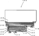
以下、本発明の具体的実施態様例について図1を用いて説明する。図1には、サファイア基板104上にn型窒化物半導体、p型窒化物半導体をそれぞれ成膜させた後、p型窒化物半導体を部分的にエッチングさせn型窒化物半導体層の表面まで露出させる。p型及びn型窒化物半導体上に電極110、111、112を形成させた後、プラズマCVD法により酸化珪素を全面に成膜する。酸化珪素をマスクを利用したエッチングにより、電極表面の一部を露出させ第1層101としての絶縁膜を形成させた。次に、白金をスパッタリング法により成膜させ、第1層上に金属層102を形成させる。さらに、第1層101と同様にして、酸化珪素をプラズマCVD法により絶縁性の第2層103として成膜させ三層構成の保護膜を形成させた。形成させたフリップチップ型光半導体素子の電極と、駆動回路基板の電極パターンとをCu含有のエポキシ樹脂を用いて電気的に接続させた。駆動回路から電流を供給するとLEDチップが発光する。LEDチップからの光はサファイアを直接透過して外部に取り出させるものの他、保護膜を形成する金属層により反射されサファイア取り出されるものがある。そのため、LEDチップからの発光波長を高効率で放出することができる。以下、本発明の各構成について詳述する。 Hereinafter, a specific embodiment example of the present invention will be described with reference to FIG. In FIG. 1, after an n-type nitride semiconductor and a p-type nitride semiconductor are formed on a sapphire substrate 104, the p-type nitride semiconductor is partially etched and exposed to the surface of the n-type nitride semiconductor layer. Let After electrodes 110, 111, and 112 are formed on the p-type and n-type nitride semiconductors, silicon oxide is formed on the entire surface by plasma CVD. A part of the electrode surface was exposed by etching using silicon oxide as a mask to form an insulating film as the first layer 101. Next, platinum is deposited by a sputtering method, and the metal layer 102 is formed on the first layer. Further, in the same manner as the first layer 101, silicon oxide was formed as an insulating second layer 103 by plasma CVD to form a protective film having a three-layer structure. The electrode of the formed flip-chip type optical semiconductor element and the electrode pattern of the drive circuit board were electrically connected using a Cu-containing epoxy resin. When a current is supplied from the drive circuit, the LED chip emits light. In addition to the light from the LED chip that is directly transmitted through the sapphire and extracted to the outside, there is the light that is reflected by the metal layer forming the protective film and extracted from the sapphire. Therefore, the emission wavelength from the LED chip can be emitted with high efficiency. Hereafter, each structure of this invention is explained in full detail.
(保護膜)
本発明の保護膜は、少なくとも絶縁性被膜からなる第1層101、金属層102、絶縁性被膜103からなる第2層で構成されている。特に、保護膜は少なくとも光半導体素子の半導体接合部をフリップチップ型光半導体素子の導通時に利用される導電性ペーストや半田などの接触から防止するものである。したがって、各層は以下の如き特性を持っていることが好ましい。
(Protective film)
The protective film of the present invention includes at least a first layer 101 made of an insulating film, a metal layer 102, and a second layer made of an insulating film 103. In particular, the protective film prevents at least the semiconductor junction of the optical semiconductor element from being contacted with a conductive paste or solder used when the flip chip type optical semiconductor element is conducted. Accordingly, each layer preferably has the following characteristics.
(第1層101、201、301)
第1層としては窒化物半導体と接して形成することができるため、窒化物半導体との密着性が良いものが好ましい。また、第1層101上に金属層102を形成するために絶縁性の高い絶縁膜が好ましい。第1層101は発光素子が発光する波長を効率よく反射する或いは、受光素子が受光する波長に対して効率よく反射することで光利用効率を高めることができる。具体的には、第1層101の膜厚を発光素子の発光波長や受光素子の受光波長に対し1/4倍の厚さとすることで反射率を向上させることができる。また、発光素子から放出された発光波長を金属層102で反射させる場合は、第1層101が少なくとも発光素子から放出される発光波長や受光素子で受光される受光波長に対して透光性の高い層とすることが好ましい。
(
Since the first layer can be formed in contact with the nitride semiconductor, a layer having good adhesion to the nitride semiconductor is preferable. In addition, an insulating film with high insulating properties is preferable in order to form the metal layer 102 over the first layer 101. The first layer 101 can efficiently reflect the wavelength emitted by the light emitting element, or can efficiently reflect the wavelength received by the light receiving element, thereby increasing the light utilization efficiency. Specifically, the reflectance can be improved by setting the thickness of the first layer 101 to ¼ times the light emission wavelength of the light emitting element and the light receiving wavelength of the light receiving element. In addition, when the emission wavelength emitted from the light emitting element is reflected by the metal layer 102, the first layer 101 is transparent to at least the emission wavelength emitted from the light emitting element and the light receiving wavelength received by the light receiving element. A high layer is preferable.
このような第1層101に用いられる材料としては、酸化珪素、酸化チタン、酸化ニオブ、酸化ハフニウム、酸化アルミニウム、酸化ジルコニウム及び窒化珪素などの金属酸化物や金属窒化物、さらにはポリイミドなどの樹脂が好適に挙げられる。第1層101が無機絶縁膜の場合はスパッタリング法や各種CVD法などを利用することにより、小型な光半導体素子においても制御性よく形成することができる。特に、緻密な無機絶縁膜を成膜させるためはプラズマCVD法を利用することが好ましい。 Examples of the material used for the first layer 101 include metal oxides and metal nitrides such as silicon oxide, titanium oxide, niobium oxide, hafnium oxide, aluminum oxide, zirconium oxide, and silicon nitride, and resins such as polyimide. Are preferable. When the first layer 101 is an inorganic insulating film, it can be formed with good controllability even in a small optical semiconductor element by utilizing a sputtering method or various CVD methods. In particular, in order to form a dense inorganic insulating film, it is preferable to use a plasma CVD method.
(金属層102、202、302)
金属層102は導電時に保護膜を構成する第2層103を介して進入する外部などからの金属イオンなどを実質的に防止する働きをするものである。金属層102は、スパッタリング法や真空蒸着法などにより薄膜、かつ制御性良く形成することができる他、欠陥の少ない膜として形成しやすい。また、第1層101を透過した波長を効率よく反射する金属(合金や積層物を含む)を選択することにより、集光性等を高め光取りだし効率を高めることができる。
(Metal layer 102, 202, 302)
The metal layer 102 functions to substantially prevent metal ions from the outside entering through the second layer 103 constituting the protective film during conduction. The metal layer 102 can be formed as a thin film with good controllability by a sputtering method, a vacuum evaporation method, or the like, and is easily formed as a film with few defects. Further, by selecting a metal (including an alloy or a laminate) that efficiently reflects the wavelength transmitted through the first layer 101, it is possible to improve light collecting efficiency and increase light extraction efficiency.
このような金属層102は外部からのイオンの進入を止める。或いは、導電性ペースト、導電性ペーストを構成するフィラや半田の進入を防止しうるものであれば種々の金属でも選択することができる。金属層の具体的材料としては、ニッケル、白金、金、アルミニウム、タングステン、モリブデンやこれらの合金や積層物が好適に挙げられる。 Such a metal layer 102 stops the entry of ions from the outside. Alternatively, various metals can be selected as long as the conductive paste, the filler constituting the conductive paste, and the solder can be prevented from entering. Specific examples of the material for the metal layer include nickel, platinum, gold, aluminum, tungsten, molybdenum, alloys and laminates thereof.
金属層はイオンマイグレーションを好適に防止しうるものであるため、金属層自体がイオン化し難いものが好ましい。特に、銀は、導電性が高く、窒化物半導体のバンドギャップに対応する光に対して反射性はよい。しかし、イオンマイグレーションを起こしやすい銀を除いた金属元素で構成することが好ましい。また、金属層102の厚みは発光素子からの発光波長を反射及び小型化などを考慮すると百Åから数ミクロン程度の厚みで形成することが好ましい。金属層102は短絡しない限り、窒化物半導体の全周を被覆するように形成しても良いし、複数に分割した形状で形成することもできる。 Since the metal layer can suitably prevent ion migration, it is preferable that the metal layer itself is not easily ionized. In particular, silver is highly conductive and has good reflectivity with respect to light corresponding to the band gap of a nitride semiconductor. However, it is preferable to use a metal element excluding silver that easily causes ion migration. The thickness of the metal layer 102 is preferably about 100 to several microns in consideration of reflection and miniaturization of the light emission wavelength from the light emitting element. As long as the metal layer 102 is not short-circuited, the metal layer 102 may be formed so as to cover the entire circumference of the nitride semiconductor, or may be formed in a plurality of divided shapes.
複数に分割された場合、p型或いはn型の電極の一部を構成することもできる。これにより、電極形成と同時に金属層302を形成することができる。そのため複数のマスクとエッチング工程を簡略して、工程数を低減することができる。このような金属層302として具体的にはp型窒化物半導体の電極として機能させる場合は、オーミック接触等を考慮して、ニッケル、コバルト、金や白金などの金属元素で構成されていることが好ましい。同様に、n型窒化物半導体の電極としても機能させる場合は、タングステン、アルミニウムやチタンなどの金属元素で構成されていることが好ましい。さらに、窒化物半導体を活性層を介してダブルへテロ構造としたLEDに利用した場合、活性層の端面から放出される光が特に多いことから活性層を絶縁層を介した金属層で被覆することにより、発光効率をより向上させることができる。 When divided into a plurality of parts, a part of the p-type or n-type electrode may be formed. Thereby, the metal layer 302 can be formed simultaneously with the electrode formation. Therefore, a plurality of masks and etching processes can be simplified, and the number of processes can be reduced. When the metal layer 302 specifically functions as an electrode of a p-type nitride semiconductor, the metal layer 302 is made of a metal element such as nickel, cobalt, gold, or platinum in consideration of ohmic contact or the like. preferable. Similarly, in the case of functioning also as an electrode of an n-type nitride semiconductor, it is preferably composed of a metal element such as tungsten, aluminum or titanium. Further, when a nitride semiconductor is used for an LED having a double hetero structure through an active layer, the active layer is covered with a metal layer through an insulating layer because particularly a large amount of light is emitted from the end face of the active layer. As a result, the luminous efficiency can be further improved.
(第2層103)
第2層103は金属層102を被覆する絶縁被膜であり外部と窒化物半導体とを電気的に絶縁するために設けられるものである。したがって、金属層102上に直接形成される場合は金属層102と密着性がよく絶縁性が高いことが求められる。第2層103に用いられる材料としては、第1層101と同様、種々の金属酸化物、金属窒化物などの無機物質の他、有機樹脂を種々選択することができる。より具体的には、酸化珪素、酸化チタン、酸化ニオブ、酸化ハフニウム、酸化アルミニウム、酸化ジルコニウム、窒化珪素及びポリイミド樹脂などを好適に挙げることができる。第2層103が無機絶縁膜の場合は緻密に形成させるほど短絡の傾向が減少するが、緻密に形成させるためには成膜時間がかかる傾向にある。
(Second layer 103)
The second layer 103 is an insulating film that covers the metal layer 102 and is provided to electrically insulate the outside from the nitride semiconductor. Therefore, when it is directly formed on the metal layer 102, it is required to have good adhesion to the metal layer 102 and high insulation. As the material used for the second layer 103, various organic resins can be selected in addition to various inorganic substances such as metal oxides and metal nitrides as in the first layer 101. More specifically, silicon oxide, titanium oxide, niobium oxide, hafnium oxide, aluminum oxide, zirconium oxide, silicon nitride, polyimide resin, and the like can be preferably exemplified. In the case where the second layer 103 is an inorganic insulating film, the tendency to short circuit decreases as it is formed more densely, but in order to form it more densely, it tends to take a longer film formation time.
一方、第2層103はフリップチップ型光半導体素子の最外郭に配置される場合がある。このような、第2層103の場合は実装時における保護膜の損傷を防止するため、ポリイミドなどの絶縁性有機物質を使用することもできる。これにより、信頼性を更に向上させることもできる。具体的には、窒化物半導体は、サファイア基板などの上に形成させた後、粘着シート上でスクライブなどにより個々の窒化物半導体素子に分割される。分割された窒化物半導体素子が取り上げ可能なように粘着シートをのばし、粘着シート下部から突き上げピンによって個々の半導体素子を突き上げ、コレットに吸着する。他方、搭載させる駆動基板側の電極にAgペーストなどの導電性ペーストを塗布する。コレットによって吸着した窒化物半導体素子を導電性ペースト上に乗せ、導電性接着剤を硬化させる。これによって、所望の駆動基板上などに窒化物半導体素子を配置固定することができる。 On the other hand, the second layer 103 may be disposed on the outermost periphery of the flip chip type optical semiconductor element. In the case of the second layer 103, an insulating organic material such as polyimide can be used to prevent damage to the protective film during mounting. Thereby, the reliability can be further improved. Specifically, after a nitride semiconductor is formed on a sapphire substrate or the like, it is divided into individual nitride semiconductor elements by scribing or the like on an adhesive sheet. The pressure-sensitive adhesive sheet is extended so that the divided nitride semiconductor elements can be picked up, and the individual semiconductor elements are pushed up from the lower part of the pressure-sensitive adhesive sheet by push-up pins and adsorbed to the collet. On the other hand, a conductive paste such as an Ag paste is applied to the electrode on the drive substrate to be mounted. The nitride semiconductor element adsorbed by the collet is placed on the conductive paste, and the conductive adhesive is cured. Thereby, the nitride semiconductor element can be arranged and fixed on a desired drive substrate or the like.
窒化物半導体素子の場合、比較的硬いサファイア基板などの上に窒化物半導体が形成される。そのため、基板側においては比較的強度が高いものの、コレットで吸着させる際、突き上げピンは絶縁被膜を形成させた電極面側を突き上げる。そして半導体面(サファイア基板に対して窒化物半導体側)を配線基板の導電部に導電性接着剤を介してフリップチップボンディングさせる。 In the case of a nitride semiconductor element, a nitride semiconductor is formed on a relatively hard sapphire substrate or the like. For this reason, although the strength is relatively high on the substrate side, the push-up pin pushes up the electrode surface side on which the insulating film is formed when it is attracted by the collet. Then, the semiconductor surface (the nitride semiconductor side with respect to the sapphire substrate) is flip-chip bonded to the conductive portion of the wiring substrate via a conductive adhesive.
この場合、短絡不良を防止するために窒化物半導体面、窒化物半導体端面及び露出している基板面等に絶縁膜を形成しているにも関わらず、短絡不良の発生率がかなり高くなる傾向がある。この原因として、発光面が基板面の時は基板が硬いために突き上げピンによって傷や割れが発生し難い。特に、窒化物半導体面側を突き上げピンによって突き上げる場合は、保護膜に傷や割れ等が発生し易くなるために短絡の発生率が高いものと考えられる。 In this case, the occurrence rate of short-circuit failure tends to be considerably high despite the formation of an insulating film on the nitride semiconductor surface, the nitride semiconductor end surface, and the exposed substrate surface in order to prevent short-circuit failure. There is. As a cause of this, when the light emitting surface is the substrate surface, since the substrate is hard, scratches and cracks are hardly generated by the push-up pins. In particular, when the nitride semiconductor surface side is pushed up by a push-up pin, scratches and cracks are likely to occur in the protective film, so it is considered that the occurrence rate of a short circuit is high.
そこで、有機樹脂による絶縁被膜を特に第2層103として形成させた場合はフリップチップボンディング形式の窒化物半導体素子において、突き上げピンによる窒化物半導体面の傷及び絶縁膜の割れを防止し、短絡不良がなく信頼性の高い窒化物半導体素子とすることができる。 Therefore, when an insulating film made of an organic resin is formed as the second layer 103 in particular, in a nitride semiconductor element of a flip chip bonding type, scratches on the nitride semiconductor surface due to push pins and cracking of the insulating film are prevented, and short circuit failure Therefore, a highly reliable nitride semiconductor device can be obtained.
即ち、第2層103を有機絶縁膜とすることにより、配線基板への実装時における粘着シート下部からの突き上げピンの物理的衝撃を緩和し、短絡の原因となる絶縁膜の割れ等を効果的に防止できるものである。このような、第2層103にポリイミド系薄膜を利用した場合における具体的な膜厚は、突き上げピンで突き上げた時に受ける物理的力の緩和、及び絶縁膜の耐圧の点で1〜10μmとすることが好ましい。また、ポリイミド系薄膜の発光主波長における透過率が60%以下であると、窒化物半導体素子端面からの漏光を抑制、光学特性のばらつきの軽減される。そのため、配光特性の安定性が得られるためより好ましい。 That is, the second layer 103 is made of an organic insulating film, so that the physical impact of the push-up pin from the lower part of the adhesive sheet during mounting on the wiring board is alleviated, and the cracking of the insulating film causing a short circuit is effective. Can be prevented. When a polyimide thin film is used for the second layer 103 as described above, the specific film thickness is 1 to 10 μm in terms of relaxation of the physical force received when pushed up by the push-up pin and the breakdown voltage of the insulating film. It is preferable. In addition, when the transmittance of the polyimide thin film at the emission main wavelength is 60% or less, light leakage from the end face of the nitride semiconductor element is suppressed, and variations in optical characteristics are reduced. Therefore, it is more preferable because the stability of the light distribution characteristic is obtained.
(光半導体素子)
本発明の光半導体素子は、窒化物半導体からなる受光素子や発光素子である。透光性絶縁基板上に形成され少なくとも半導体接合を有する窒化物半導体により構成することができる。具体的には、透光性絶縁基板上にMOCVD法やHVPE法を用いて窒化物半導体を形成させることができる。このような透光性絶縁基板としては、窒化ガリウム、サファイア(Al2O3)やスピネル(MgAl2O4)などが挙げられる。半導体接合としては、MIS接合、PIN接合の他、pn接合が挙げられる。また、光半導体素子の特性により、ホモやダブルへテロ構造とすることができる。さらに、単一量子井戸構造や多重量子井戸構造とすることもできる。
(Optical semiconductor device)
The optical semiconductor element of the present invention is a light receiving element or a light emitting element made of a nitride semiconductor. A nitride semiconductor formed on a light-transmitting insulating substrate and having at least a semiconductor junction can be used. Specifically, a nitride semiconductor can be formed on a light-transmitting insulating substrate using MOCVD or HVPE. Examples of such a light-transmitting insulating substrate include gallium nitride, sapphire (Al 2 O 3 ), spinel (MgAl 2 O 4 ), and the like. Examples of the semiconductor junction include a pn junction in addition to a MIS junction and a PIN junction. Further, depending on the characteristics of the optical semiconductor element, a homo or double hetero structure can be formed. Furthermore, a single quantum well structure or a multiple quantum well structure can be used.
pin接合やpn接合が短絡することで、半導体特性に大きな損傷が加わる。そのため、本発明が有効に働くことになる。半導体の材料やその混晶度によって光半導体素子の発光波長及び受光波長を紫外光から赤色領域まで種々選択することができる。 When the pin junction or the pn junction is short-circuited, the semiconductor characteristics are greatly damaged. Therefore, the present invention works effectively. The light emission wavelength and light reception wavelength of the optical semiconductor element can be variously selected from the ultraviolet light to the red region depending on the semiconductor material and the crystallinity thereof.
なお結晶性の良い窒化物半導体を形成させるためにはサファイヤ基板を用いることが好ましい。このサファイヤ基板上に格子不整合緩和のためにGaN、AlN等のバッファー層を形成しその上にpn接合などを有する窒化物半導体を形成させることにより半導体特性の優れた発光素子や受光素子を構成させることができる。サファイアで基板を形成させると硬度が高く、基板自体が透光性を持つと共に外部からの水分等の進入を防ぐことができるため特に好ましい。 In order to form a nitride semiconductor with good crystallinity, a sapphire substrate is preferably used. A light-emitting element and a light-receiving element having excellent semiconductor characteristics are formed by forming a buffer layer of GaN, AlN or the like on this sapphire substrate and forming a nitride semiconductor having a pn junction or the like on the buffer layer. Can be made. Forming the substrate with sapphire is particularly preferable because it has high hardness, the substrate itself has translucency, and can prevent entry of moisture and the like from the outside.
窒化物半導体は、不純物をドープしない状態でn型導電性を示すが、n型ドーパントとしてSi、Ge、Se、Te、Sn等を適宜導入することが好ましい。また、n型ドーパントと微量のp型ドーパントとをドーピングしたダブルドーピングすることもできる。これらのドーパントの種類とドーピング量を変えることによってキヤリア密度を制御し電気抵抗を下げることができる。一方、p型窒化物半導体を形成させる場合は、p型ドーパントであるZn、Mg、Be、Ca、Sr、Ba等をドープさせる。窒化ガリウム半導体は、p型ドーパントをドープしただけでは低抵抗化しにくいためp型ドーパント導入後に、低速電子線照射、プラズマ照射や熱処理等させることで低抵抗化処理することができる。 The nitride semiconductor exhibits n-type conductivity without being doped with impurities, but it is preferable to appropriately introduce Si, Ge, Se, Te, Sn or the like as an n-type dopant. Moreover, double doping which doped the n-type dopant and the trace amount p-type dopant can also be performed. By changing the kind and amount of these dopants, the carrier density can be controlled and the electrical resistance can be lowered. On the other hand, when forming a p-type nitride semiconductor, the p-type dopants such as Zn, Mg, Be, Ca, Sr, and Ba are doped. A gallium nitride semiconductor cannot be reduced in resistance simply by doping with a p-type dopant, and thus can be subjected to low-resistance treatment by low-energy electron beam irradiation, plasma irradiation, heat treatment, or the like after introduction of the p-type dopant.
半導体露出面側に一対の電極を形成するためには各半導体を所望の形状にエッチングしてあることが好ましい。エッチングとしては、ドライエッチングや、ウエットエッチングがある。ドライエッチングとしては例えば反応性イオンエッチング、イオンミリング、集束ビームエッチング、ECRエッチング等が挙げられる。又、ウエットエッチングとしては、硝酸と燐酸の混酸を用いることができる。ただし、エッチングを行う前に所望の形状に窒化珪素や酸化珪素等の材料を用いてマスクを形成することは言うまでもない。以下、本発明の実施例について詳述するがこれのみに限定されるものでないことはいうまでもない。 In order to form a pair of electrodes on the semiconductor exposed surface side, each semiconductor is preferably etched into a desired shape. Etching includes dry etching and wet etching. Examples of dry etching include reactive ion etching, ion milling, focused beam etching, and ECR etching. As wet etching, a mixed acid of nitric acid and phosphoric acid can be used. However, it goes without saying that a mask is formed in a desired shape using a material such as silicon nitride or silicon oxide before etching. Hereinafter, although the Example of this invention is described in full detail, it cannot be overemphasized that it is not limited only to this.
(実施例1)
洗浄されたサファイアのC面を成膜表面としてMOCVD法を用いて窒化物半導体を成膜した。成膜装置内にサファイア基板104を配置し650℃に加熱すると共に、TMG(トリメチルガリウム)ガス、窒素ガスを原料ガス、水素ガスをキャリアガスとして流しバッファ層105を形成させた。一旦、原料ガスの導入を止めた後、成膜温度を1150℃に上げTMGガス、窒素ガス、水素ガスにn型ドーパントガスとしてシランを加えて厚さ5μmのn型窒化ガリウム層106を成膜した。次に、TMGガスの供給を停止し、成膜温度を800℃に低下させた後、TMGガス、TMA(トリメチルアルミニウム)ガス、窒素ガス及び水素ガスを供給させて厚さ3nmの窒化インジウムガリウムを発光層107として成膜させた。
Example 1
A nitride semiconductor was formed by MOCVD using the cleaned C-plane of sapphire as the film-forming surface. The sapphire substrate 104 was placed in the film forming apparatus and heated to 650 ° C., and a
次に、原料ガスの供給を停止して成膜温度を1050℃に上げた後、再び原料ガスとしてTMGガス、TMAガス、窒素ガス、キャリアガスとして水素ガス、不純物ガスとしてシクロペンタジエチルマグネシウムを加えて厚さ300Åのp型クラッド層108を成膜させる。
Next, after the supply of the source gas is stopped and the film formation temperature is raised to 1050 ° C., TMG gas, TMA gas, nitrogen gas, hydrogen gas as the carrier gas, and cyclopentadiethyl magnesium as the impurity gas are added again. A p-
p型クラッド層108上にTMAガスの供給を停止した以外はp型クラッド層の形成と同様にして厚さ1500Åのp型コンタクト層109を成膜させる。(なお、p型窒化物半導体となる半導体層は成膜後400℃以上で熱処理してある。)こうして活性層を介してダブルへテロ構造である窒化物半導体を成膜した。半導体ウエハの同一面側に電極を形成させるため、マスクを利用して、活性層、p型クラッド層、p型コンタクト層を一部残しつつn型コンタクト層まで、部分的にエッチングさせてある。同様に各LEDチップとして分離できる大きさでサファイア基板上までそれぞれエッチングしてある。エッチング後、サファイア基板上には島状の窒化物半導体層が形成されることとなる。
A p-
p型コンタクト層109と接触し全面を被覆する電極110として白金を500Åでスパッタリング法を用いて成膜した。この電極110上には、100μm角のp型電極111として白金を0.7μmで成膜した。n型コンタクト層106上には直径100μmのn型電極112としてタングステン/アルミニウムを200Å/0.7μmとして成膜した。これによって、島状の窒化物半導体上には同一平面側に正負一対の電極111、112が形成されたことになる。
As an electrode 110 that is in contact with the p-
各窒化物半導体が形成されたp型及びn型の各電極上に第1層101を形成すべく、半導体ウエハをプラズマCVD装置内に配置させた。シランガス及び酸化窒素ガスを原料ガスとして酸化珪素膜を半導体ウエハの全面に形成させた。酸化珪素膜を形成後、プラズマCVD装置から取り出し、レジストマスクを利用してドライエッチングさせることによりp型電極111及びn型電極112の表面を露出させた。レジストマスクを除去して半導体ウエハ上に第1層101となる酸化珪素膜が形成させた。 In order to form the first layer 101 on each of the p-type and n-type electrodes on which each nitride semiconductor was formed, the semiconductor wafer was placed in a plasma CVD apparatus. A silicon oxide film was formed on the entire surface of the semiconductor wafer using silane gas and nitrogen oxide gas as source gases. After forming the silicon oxide film, the silicon oxide film was taken out from the plasma CVD apparatus and subjected to dry etching using a resist mask to expose the surfaces of the p-type electrode 111 and the n-type electrode 112. The resist mask was removed, and a silicon oxide film to be the first layer 101 was formed on the semiconductor wafer.
続いて、半導体ウエハをスパッタリング装置内に配置させ、ターゲットをプラチナとしスパッタリングすることにより、金属層102となる厚さ500Åのプラチナを成膜させた。リフトオフによりp型電極111及びn型電極112の表面を露出させた。さらに、第1層101と同様の条件で再び第2層102の酸化珪素を形成させる。その後、p型電極111及びn型電極112に形成されたマスクを除去する。これにより、各p型電極111、n型電極112の表面及びサファイア基板104以外は窒化物半導体の表面には、酸化珪素101、プラチナ102、酸化珪素103の三層構成となる保護膜が形成される。半導体ウエハを分離することにより、各々フリップチップ型LEDを得ることができる。 Subsequently, the semiconductor wafer was placed in a sputtering apparatus, and sputtering was performed using platinum as a target, thereby forming a platinum layer having a thickness of 500 mm to be the metal layer 102. The surfaces of the p-type electrode 111 and the n-type electrode 112 were exposed by lift-off. Further, silicon oxide for the second layer 102 is formed again under the same conditions as those for the first layer 101. Thereafter, the mask formed on the p-type electrode 111 and the n-type electrode 112 is removed. Thus, a protective film having a three-layer structure of silicon oxide 101, platinum 102, and silicon oxide 103 is formed on the surface of the nitride semiconductor except the surface of each p-type electrode 111 and n-type electrode 112 and the sapphire substrate 104. The By separating the semiconductor wafer, each flip-chip type LED can be obtained.
得られたLEDチップの内、1400個を電極の間隔が約100μである一対の電極が形成された駆動回路上にAgペーストを用いてダイボンディングさせた。各LEDに電流を流したところサファイア基板104を介して発光しており全て発光可能であった。 Of the obtained LED chips, 1400 were die-bonded using Ag paste on a drive circuit on which a pair of electrodes having an electrode interval of about 100 μm was formed. When an electric current was passed through each LED, light was emitted through the sapphire substrate 104 and all light was emitted.
(比較例1)
金属層、第2層を設けるかわりに第1層の厚みを実施例1の保護膜の厚みと同じ膜厚とした以外は同様にして図4の如き、フリップチップ型LEDを形成させた。実施例1と同様に駆動回路上にAgペーストを用いて1400個のLEDをダイボンディングさせた。各LEDに電流を流したところ不灯となったものが5個あった。また、発光輝度が極端に暗くなったものが8個あった。不灯となったものを集束イオンビーム加工装置を用いて調べたところ、保護膜を介してAgが貫通しているためにリークしていた。また、発光輝度が極端に暗くなったものを除いた平均輝度を100とした場合、実施例1の平均輝度は121であった。
(Comparative Example 1)
Instead of providing the metal layer and the second layer, a flip-chip type LED as shown in FIG. 4 was formed in the same manner except that the thickness of the first layer was the same as the thickness of the protective film of Example 1. As in Example 1, 1400 LEDs were die-bonded on the drive circuit using Ag paste. There were five lamps that were unlit when a current was passed through each LED. In addition, there were 8 light emitting luminances that were extremely dark. When the non-lighted thing was investigated using the focused ion beam processing apparatus, it was leaking because Ag penetrated through the protective film. In addition, when the average brightness excluding that in which the light emission brightness was extremely dark was 100, the average brightness in Example 1 was 121.
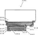
(実施例2)
実施例2は図2に示したLEDの如く、第2層203を酸化珪素で形成させるかわりにポリイミド被膜とした。ポリイミド被膜を塗布硬化して第2層203を形成させた以外は、実施例1と同様にしてフリップチップ型LEDを構成させた。得られたLEDを実施例1、比較例1と同様にして測定したところ実施例1とほぼ同様の結果が得られた。なお、実施例2は実施例1に対して経時劣化が少なくなる傾向にある。
(Example 2)
In Example 2, a polyimide film was used instead of forming the
(実施例3)
金属層302の厚みを0.7μmとして図3の如く、p型電極として一体的に形成させた以外は、実施例1と同様にしてフリップチップ型LEDを形成させた。得られたLEDは工程を簡略化したにもかかわらず、実施例1とほぼ同様の信頼性を得ることができた。
(Example 3)
A flip chip type LED was formed in the same manner as in Example 1 except that the thickness of the metal layer 302 was 0.7 μm and was integrally formed as a p-type electrode as shown in FIG. Although the obtained LED simplified the process, it was possible to obtain almost the same reliability as in Example 1.
100、200、300・・・光半導体素子
101、201、301・・・無機絶縁膜からなる第1層
102、202・・・金属層
103、303・・・無機絶縁膜からなる第2層
104、204、304・・・透光性絶縁基板
105、205、305・・・バッファ層
106、206、306・・・n型コンタクト層
107、207、307・・・活性層
108、208、308・・・p型クラッド層
109、209、309・・・p型コンタクト層
110、210、310・・・p型半導体上に形成された電極
111、211・・・p型電極
112、212、312・・・n型電極
203・・・有機絶縁膜からなる第2層
214・・・駆動基板上に形成された電極パターン
215・・・駆動基板
302・・・p型電極を構成する金属層
400・・・光半導体素子
401・・・無機絶縁膜からなる第1層
404・・・透光性絶縁基板
405・・・バッファ層
406・・・n型コンタクト層
407・・・活性層
408・・・p型クラッド層
409・・・p型コンタクト層
410・・・p型半導体上に形成された電極
411・・・p型電極
412・・・n型電極
100, 200, 300 ...
Claims (6)
前記保護膜は絶縁性被膜からなる第1層と、該第1層上の金属層と、該金属層上に絶縁性被膜からなる第2層の少なくとも3層構造を有し、
さらに前記基板上の窒化物半導体から露出された基板面に、前記保護膜が形成されていることを特徴とするフリップチップ型LED。 A flip chip type having a protective film in which positive and negative electrodes are provided on the same plane side of a nitride semiconductor formed on a light-transmitting insulating substrate, and the nitride semiconductor layer surface is covered except for an exposed portion of the electrode surface LED ,
The protective film has at least a three-layer structure of a first layer made of an insulating film, a metal layer on the first layer, and a second layer made of an insulating film on the metal layer,
Flip chip type LED further the substrate surface that is exposed from the nitride semiconductor of the substrate, wherein the protective film is formed.
Priority Applications (1)
| Application Number | Priority Date | Filing Date | Title |
|---|---|---|---|
| JP2003354383A JP4474892B2 (en) | 2003-10-14 | 2003-10-14 | Flip chip type LED |
Applications Claiming Priority (1)
| Application Number | Priority Date | Filing Date | Title |
|---|---|---|---|
| JP2003354383A JP4474892B2 (en) | 2003-10-14 | 2003-10-14 | Flip chip type LED |
Related Parent Applications (1)
| Application Number | Title | Priority Date | Filing Date |
|---|---|---|---|
| JP14187398A Division JP3531475B2 (en) | 1998-05-22 | 1998-05-22 | Flip chip type optical semiconductor device |
Publications (3)
| Publication Number | Publication Date |
|---|---|
| JP2004080050A JP2004080050A (en) | 2004-03-11 |
| JP2004080050A5 JP2004080050A5 (en) | 2005-09-08 |
| JP4474892B2 true JP4474892B2 (en) | 2010-06-09 |
Family
ID=32025889
Family Applications (1)
| Application Number | Title | Priority Date | Filing Date |
|---|---|---|---|
| JP2003354383A Expired - Fee Related JP4474892B2 (en) | 2003-10-14 | 2003-10-14 | Flip chip type LED |
Country Status (1)
| Country | Link |
|---|---|
| JP (1) | JP4474892B2 (en) |
Families Citing this family (14)
| Publication number | Priority date | Publication date | Assignee | Title |
|---|---|---|---|---|
| WO2006035664A1 (en) | 2004-09-27 | 2006-04-06 | Matsushita Electric Industrial Co., Ltd. | Semiconductor light emitting element, manufacturing method and mounting method of the same and light emitting device |
| JP4297084B2 (en) | 2005-06-13 | 2009-07-15 | 住友電気工業株式会社 | LIGHT EMITTING DEVICE MANUFACTURING METHOD AND LIGHT EMITTING DEVICE |
| US20070215998A1 (en) * | 2006-03-20 | 2007-09-20 | Chi Lin Technology Co., Ltd. | LED package structure and method for manufacturing the same |
| JP4770745B2 (en) * | 2007-01-23 | 2011-09-14 | 三菱電機株式会社 | Semiconductor light emitting device |
| KR101571577B1 (en) | 2008-02-29 | 2015-11-24 | 오스람 옵토 세미컨덕터스 게엠베하 | Monolithic, optoelectronic semi-conductor body and method for the production thereof |
| DE102008011848A1 (en) | 2008-02-29 | 2009-09-03 | Osram Opto Semiconductors Gmbh | Optoelectronic semiconductor body and method for producing such |
| CN101834236B (en) * | 2009-03-11 | 2013-02-13 | 晶元光电股份有限公司 | Luminescent device |
| US8471282B2 (en) | 2010-06-07 | 2013-06-25 | Koninklijke Philips Electronics N.V. | Passivation for a semiconductor light emitting device |
| CN105742447B (en) * | 2010-11-18 | 2019-03-26 | 首尔伟傲世有限公司 | Light emitting diode with electrode pad |
| JP2013021175A (en) * | 2011-07-12 | 2013-01-31 | Toshiba Corp | Semiconductor light-emitting element |
| JP5985322B2 (en) | 2012-03-23 | 2016-09-06 | 株式会社東芝 | Semiconductor light emitting device and manufacturing method thereof |
| JP2014096539A (en) * | 2012-11-12 | 2014-05-22 | Tokuyama Corp | Ultraviolet light-emitting element, and light-emitting structure |
| JP2015079929A (en) * | 2013-09-11 | 2015-04-23 | 株式会社東芝 | Semiconductor light-emitting device and method of manufacturing the same |
| JP7117136B2 (en) | 2018-04-20 | 2022-08-12 | スタンレー電気株式会社 | Light-emitting element and light-emitting device |
Family Cites Families (7)
| Publication number | Priority date | Publication date | Assignee | Title |
|---|---|---|---|---|
| JPH03203388A (en) * | 1989-12-29 | 1991-09-05 | Matsushita Electric Ind Co Ltd | Semiconductor light emitting element and its manufacture |
| JP3136672B2 (en) * | 1991-07-16 | 2001-02-19 | 豊田合成株式会社 | Gallium nitride based compound semiconductor light emitting device |
| US5358880A (en) * | 1993-04-12 | 1994-10-25 | Motorola, Inc. | Method of manufacturing closed cavity LED |
| JPH09153644A (en) * | 1995-11-30 | 1997-06-10 | Toyoda Gosei Co Ltd | Group-iii nitride semiconductor display device |
| JP3264163B2 (en) * | 1996-01-18 | 2002-03-11 | 日亜化学工業株式会社 | Nitride semiconductor laser device |
| JPH1197742A (en) * | 1997-09-22 | 1999-04-09 | Nichia Chem Ind Ltd | Nitride semiconductor element |
| JP3322300B2 (en) * | 1997-11-14 | 2002-09-09 | 日亜化学工業株式会社 | Gallium nitride based semiconductor light emitting device and light receiving device |
-
2003
- 2003-10-14 JP JP2003354383A patent/JP4474892B2/en not_active Expired - Fee Related
Also Published As
| Publication number | Publication date |
|---|---|
| JP2004080050A (en) | 2004-03-11 |
Similar Documents
| Publication | Publication Date | Title |
|---|---|---|
| JP3531475B2 (en) | Flip chip type optical semiconductor device | |
| JP6386015B2 (en) | Light emitting element | |
| CN100580963C (en) | Light emitting diode having InO layer and method for manufacturing the same | |
| US7491974B2 (en) | Light-emitting device | |
| US8022430B2 (en) | Nitride-based compound semiconductor light-emitting device | |
| JP2010541224A (en) | Optoelectronic semiconductor chip, optoelectronic component, and manufacturing method of optoelectronic component | |
| CN101820043A (en) | Light-emitting device | |
| JP4474892B2 (en) | Flip chip type LED | |
| KR20070041506A (en) | Positive electrode for semiconductor light-emitting device | |
| US20040201110A1 (en) | Flip-chip light emitting diode with indium-tin-oxide based reflecting contacts | |
| CN102222744A (en) | Light emitting device, method of manufacturing the light emitting device, light emitting device package, and lighting system | |
| JP2006041403A (en) | Semiconductor luminous element | |
| KR102530758B1 (en) | Semiconductor light emitting device package | |
| JP2770717B2 (en) | Gallium nitride based compound semiconductor light emitting device | |
| US8519417B2 (en) | Light emitting device | |
| JP5471485B2 (en) | Nitride semiconductor device and pad electrode manufacturing method for nitride semiconductor device | |
| KR102413447B1 (en) | Light emitting device | |
| CN101656283B (en) | Light-emitting diode assembly and manufacturing method thereof | |
| KR20110082863A (en) | Supporting wafer for semiconductor light emitting device, method for mafacturing the same and vertical structured semiconductor light emitting device using the same | |
| US10811566B2 (en) | Light emitting device, method for producing light emitting device, and light emitting module | |
| KR101115533B1 (en) | Flip chip Light-emitting device and Method of manufacturing the same | |
| KR20150052513A (en) | LED device and package having the same | |
| KR101090178B1 (en) | Semiconductor light emitting device | |
| KR101119009B1 (en) | Method of forming light emitting device with separation by ion implantation | |
| US11888091B2 (en) | Semiconductor light emitting device and light emitting device package |
Legal Events
| Date | Code | Title | Description |
|---|---|---|---|
| A521 | Written amendment |
Free format text: JAPANESE INTERMEDIATE CODE: A523 Effective date: 20050523 |
|
| A621 | Written request for application examination |
Free format text: JAPANESE INTERMEDIATE CODE: A621 Effective date: 20050523 |
|
| A131 | Notification of reasons for refusal |
Free format text: JAPANESE INTERMEDIATE CODE: A131 Effective date: 20081111 |
|
| A521 | Written amendment |
Free format text: JAPANESE INTERMEDIATE CODE: A523 Effective date: 20090109 |
|
| A131 | Notification of reasons for refusal |
Free format text: JAPANESE INTERMEDIATE CODE: A131 Effective date: 20090609 |
|
| A521 | Written amendment |
Free format text: JAPANESE INTERMEDIATE CODE: A523 Effective date: 20090806 |
|
| TRDD | Decision of grant or rejection written | ||
| A01 | Written decision to grant a patent or to grant a registration (utility model) |
Free format text: JAPANESE INTERMEDIATE CODE: A01 Effective date: 20100216 |
|
| A01 | Written decision to grant a patent or to grant a registration (utility model) |
Free format text: JAPANESE INTERMEDIATE CODE: A01 |
|
| A61 | First payment of annual fees (during grant procedure) |
Free format text: JAPANESE INTERMEDIATE CODE: A61 Effective date: 20100301 |
|
| R150 | Certificate of patent or registration of utility model |
Free format text: JAPANESE INTERMEDIATE CODE: R150 |
|
| FPAY | Renewal fee payment (event date is renewal date of database) |
Free format text: PAYMENT UNTIL: 20130319 Year of fee payment: 3 |
|
| FPAY | Renewal fee payment (event date is renewal date of database) |
Free format text: PAYMENT UNTIL: 20130319 Year of fee payment: 3 |
|
| FPAY | Renewal fee payment (event date is renewal date of database) |
Free format text: PAYMENT UNTIL: 20130319 Year of fee payment: 3 |
|
| FPAY | Renewal fee payment (event date is renewal date of database) |
Free format text: PAYMENT UNTIL: 20140319 Year of fee payment: 4 |
|
| R250 | Receipt of annual fees |
Free format text: JAPANESE INTERMEDIATE CODE: R250 |
|
| R250 | Receipt of annual fees |
Free format text: JAPANESE INTERMEDIATE CODE: R250 |
|
| R250 | Receipt of annual fees |
Free format text: JAPANESE INTERMEDIATE CODE: R250 |
|
| R250 | Receipt of annual fees |
Free format text: JAPANESE INTERMEDIATE CODE: R250 |
|
| LAPS | Cancellation because of no payment of annual fees |