JP4471585B2 - Film formation method - Google Patents
Film formation method Download PDFInfo
- Publication number
- JP4471585B2 JP4471585B2 JP2003125617A JP2003125617A JP4471585B2 JP 4471585 B2 JP4471585 B2 JP 4471585B2 JP 2003125617 A JP2003125617 A JP 2003125617A JP 2003125617 A JP2003125617 A JP 2003125617A JP 4471585 B2 JP4471585 B2 JP 4471585B2
- Authority
- JP
- Japan
- Prior art keywords
- film
- piezoelectric
- paste
- temperature
- precursor
- Prior art date
- Legal status (The legal status is an assumption and is not a legal conclusion. Google has not performed a legal analysis and makes no representation as to the accuracy of the status listed.)
- Expired - Fee Related
Links
Images


Description
【0001】
【発明の属する技術分野】
本発明は、膜形成手法により被膜形成体の表面上にペーストを用いて所定のパターンの膜を形成する膜形成方法に関し、特に、スクリーン印刷等の厚膜形成手法による膜形成方法に関する。
【0002】
【従来の技術】
従来より、スクリーン印刷等の厚膜形成手法により被膜形成体(ワーク)の表面上にペーストを用いて所定のパターンの膜を形成する場合、完成後の膜内に気泡が内包されないようにすること、及び、完成後の膜の表面(上面)が平らになっていることが要求されている。
【0003】
上記した完成後の膜内に気泡が内包されないようにすることを達成するため、非特許文献1に記載のスクリーン印刷装置は、内部が略真空状態となり得る真空チャンバーを備えていて、略真空状態となっている真空チャンバー内で、所定のペーストをメッシュ状の製版の開口部からスキージで押し出してワークの表面上に同ペーストを転写することで、所定のパターンの膜をスクリーン印刷するようになっている。
【0004】
これによれば、大気中等にてペーストを作製する等により作製時点におけるペースト内に気泡が内包されている場合でも、ペースト(の表面)を略真空にさらすことでスクリーン印刷開始前の時点においては同ペースト内に内包されていた気泡が除去され得(以下、気泡を除去することを「脱泡」と云うこともある。)、また、スクリーン印刷開始前の時点においてペーストが完全に脱泡されていない場合であっても、その時点以降同スクリーン印刷終了後の時点に渡ってペースト(の表面)は継続して略真空にさらされ続けているから、スクリーン印刷工程の途中で前記内包されていた気泡が完全に除去され得る。また、スクリーン印刷工程中に渡ってペースト(の表面)が略真空にさらされ続けていることで同スクリーン印刷工程中にペースト内に新たに気泡が混入することもない。従って、完成後の膜内に気泡が内包されないことを確実に達成することができる。
【0005】
【非特許文献1】
ニューロング精密工業株式会社製 真空スクリーン印刷装置
LS-340VC のカタログ(2002年5月27日 第1版発行)
【0006】
【発明が解決しようとする課題】
しかしながら、上記従来の真空スクリーン印刷装置は、スクリーン印刷を真空チャンバー内で実行するため、スクリーン印刷を実行するために必要なスキージ部そのもの、ワークをセットするためのテーブル部そのもの等の比較的大きな構造体を真空チャンバー内に配置する必要がある。従って、真空チャンバーの容積が大きくなる。この結果、真空チャンバー内の圧力を大気圧から略真空に相当する圧力まで減少させるために必要な時間が長くなるとともに、印刷装置全体が大きくなるという問題がある。
【0007】
また、ペースト(の表面)を略真空にさらすと、ペーストの粘度を調整するため同ペースト中に含まれている有機溶剤の沸点が低下して同有機溶剤が蒸発し易くなるからペーストの粘度が短時間内で変化(上昇)し易くなる。従って、ペーストの交換周期を短くする必要があることに加え、一回のスクリーン印刷工程の途中で、若しくは、同一の製版にて同一のパターンの膜を連続して複数回スクリーン印刷する場合には各スクリーン印刷工程間でペーストの粘度が変化(上昇)する可能性が高く、印刷される膜の品質(例えば、膜厚等)を一定に管理することが困難であるという問題がある。
【0008】
また、所定のペーストをメッシュ状の製版の開口部からスキージで押し出して所定のパターンの膜をスクリーン印刷する場合、印刷直後の膜の表面には前記メッシュのパターンに対応する凹凸(メッシュの跡)が不可避的に形成される。この凹凸は、大気中にペースト(膜)がさらされている場合にはペーストそのものに働く重力の作用により同ペーストが流動することで短時間内に消滅させられ、その結果、ペースト(膜)の表面は平らになり得る(以下、重力の作用により膜の表面(上面)が平らになることを「レベリング」と云うこともある。)。しかしながら、上記真空スクリーン印刷装置を利用してスクリーン印刷を行った場合、印刷直後においてペースト(膜)が略真空にさらされて有機溶剤が蒸発し易い状態が継続する期間が存在する。従って、前記期間中にペースト表面に乾燥皮膜が形成されて同表面が硬化することでレベリングが確実に達成されにくくなるという問題がある。
【0009】
一方、以上のような種々の問題を解決するため、大気中で所定のパターンの膜をペーストを用いてワーク上にスクリーン印刷し、その後の所定時間に渡ってペースト(膜)を加熱するとともに略真空にさらす技術も知られている。これによれば、ペーストを略真空にさらすことと、加熱に基づく同ペーストの粘度の低下により同ペーストの流動性が向上することが相俟って、ペースト作製時点から同ペーストに内包されている気泡、及びスクリーン印刷工程中にてペーストがワーク上に印刷される際に同ペースト内に新たに混入した気泡(従って、ペーストに内包された総ての気泡)が除去され得る。また、上記ペーストの粘度の低下による同ペーストの流動性の向上により、レベリングが一層確実に達成され易くなる。
【0010】
しかしながら、かかる技術においては、印刷されたペースト(膜)の膜厚の増加につれて、ペーストの脱泡の程度が低下するとともに、膜の外周部の形状のばらつきの程度が大きくなるという問題がある。この点について、以下、図11、及び図12を参照しながら説明する。
【0011】
図11(a)は、ワーク100の表面上に、(X軸方向の)一辺の長さ(幅)がWmask(即ち、製版に形成された長方形の開口部おける一辺の長さがWmask)の直方体状の比較的膜厚の大きい膜200を所定のペーストを用いて大気中にて一回スクリーン印刷した直後における膜200の平面図、図11(b)は、図11(a)の4−4線に沿った平面でワーク、及び膜を切断した断面図である。図11(b)に示すように、印刷直後における膜200の表面(上面)には前記メッシュのパターンに対応する凹凸(メッシュの跡)が形成されているとともに、膜200の輪郭における前記一辺に沿う方向の幅はWmaskになっている。また、膜200内には、膜200の表面(上面)に比較的近い位置に存在する気泡200aと、同膜200の表面から比較的遠い位置(従って、ワーク100の表面(上面)に比較的近い位置)に存在する気泡200bとが内包されている。
【0012】
図12(a)は、図11に示した膜200を、前記印刷後の所定時間に渡って加熱するとともに略真空にさらした後の時点における膜200の平面図、図12(b)は、図12(a)の4−4線に沿った平面でワーク、及び膜を切断した断面図である。図12(b)に示すように、この時点における膜200の表面においては先に説明したペースト(膜)の流動性の向上によりレベリングが確実に達成されている。
【0013】
また、ペーストの脱泡については、膜200の表面に比較的近い位置に存在する気泡200aは同表面から真空中へ抜け易いことから除去されている一方、膜200の表面から比較的遠い位置に存在する気泡200bは膜(ペースト)200の粘度によっては真空中に抜け難いことから除去されずに膜200内に残留している。換言すれば、印刷された膜の膜厚の増加につれて、膜内におけるワークの表面に近い位置に存在する気泡は除去されにくくなる(従って、ペーストの脱泡の程度が低下する)。
【0014】
更には、この時点においては、図12(a)(b)に示すように、膜200の外周部が平面視で(Z軸正方向から見て)膜200の外側に向けて広がる方向に変形している(図12(a)において多数の微細なドットで示した領域を参照。)。以下、本明細書において、膜の上方向から見たときにおける膜の外周部の印刷直後の時点からの膜の外側への変形量を「広がり量」と称呼する(例えば、図12(a)(b)においてw1,w2を参照。)。この広がり量は、ワーク(の表面)と膜(の表面)との性質に基づいて決定されるワークに対する膜(ペースト)の濡れの程度(濡れ性)に依存する量である。
【0015】
この広がり量には、図12(a)に示すように、膜200の外周部の位置によってばらつきが不可避的に発生する。かかる広がり量のばらつきの程度は、例えば、膜200の各辺についての広がり量の最大値と最小値の差(例えば、図12(a)(b)においてΔw1,Δw2)によって表すことができ、広がり量のばらつきの程度(例えば、Δw1,Δw2)は膜200の膜厚の増加に応じて比例的に増加する関係にある。換言すれば、印刷された膜の膜厚の増加につれて、膜の外周部の形状のばらつきの程度が大きくなる。これにより、膜の膜厚が大きくなると、膜の外観不良が発生し易くなるとともに、例えば、膜が圧電/電歪素子の前駆体である場合等においては、圧電/電歪素子が所期の性能を発揮し得なくなる可能性が高くなる。
【0016】
従って、本発明の目的は、膜形成手法(特に、スクリーン印刷等の厚膜形成手法)により被膜形成体の表面上にペーストを用いて所定のパターンの膜を形成する膜形成方法において、形成された膜の膜厚に拘わらず、膜の脱泡の程度を高く維持し、膜の外周部の形状のばらつきの程度を小さくすることができるとともに、膜表面におけるレベリングを確実に達成し得るものを提供することにある。
【0017】
【発明の概要】
本発明の膜形成方法は、第1の温度、且つ第1の圧力下にて被膜形成体の表面上に第1のペーストを用いて所定のパターンの前駆膜を形成した後、前記前駆膜を前記第1の温度よりも高い第2の温度、且つ前記第1の圧力よりも低い第2の圧力下にさらすことで少なくとも同前駆膜内に内包されている気泡を除去する第1工程と、前記第1の温度、且つ前記第1の圧力下にて前記前駆膜の表面上に第2のペーストを用いて前記所定のパターンの新たな前駆膜を重ねて形成した後、前記新たな前駆膜を前記第1の温度よりも高い第3の温度、且つ前記第1の圧力よりも低い第3の圧力下にさらすことで少なくとも同新たな前駆膜内に内包されている気泡を除去する工程を1回以上行う第2工程とを備え、複数枚の前記前駆膜から成る前記所定のパターンの(1枚の、1層の)膜を形成する方法である。
【0018】
ここにおいて、前記第1のペーストと前記第2のペーストとは同一のペースト(同一の組成(物性)を有するペースト)であってもよい。また、この場合、前記第1の温度、及び第1の圧力は、それぞれ、大気温度(常温)、及び大気圧力(常圧)であり、前記第2の温度、及び前記第3の温度は加熱により達成される温度であるとともに、前記第2の圧力、及び前記第3の圧力は真空ポンプを利用して達成される圧力(例えば、略真空に相当する圧力)であることが好適である。また、前記第2の温度と前記第3の温度とは同一の温度であってもよいし、前記第2の圧力と前記第3の圧力とは同一の圧力であってもよい。更には、前記第1工程において、前記前駆膜を前記第2の温度、且つ第2の圧力下にさらすことで同前駆膜内に内包されている気泡を除去した後、同前駆膜を乾燥させることが好適である。同様に、前記第2工程において、前記前駆膜を前記第3の温度、且つ第3の圧力下にさらすことで同前駆膜内に内包されている気泡を除去した後、同前駆膜を乾燥させることが好適である。
【0019】
これによれば、複数枚の前駆膜の各々が第1の温度、且つ第1の圧力下(例えば、大気中)にて所定の膜形成手法(例えば、スクリーン印刷)により形成される毎に、同形成された前駆膜(積み重ねられていく前駆膜のうちその時点において最上段に位置する前駆膜)がその後、第1の温度よりも高い第2(又は、第3)の温度(例えば、大気中での加熱により達成される大気温度よりも高い温度)、且つ第1の圧力よりも低い第2(又は、第3)の圧力(例えば、略真空に相当する圧力)下にさらされる。従って、先に説明したように、前駆膜を第2(又は、第3)の圧力下にさらすことと、同前駆膜を第2(又は、第3)の温度下にさらすことにより同前駆膜(第1,第2のペースト)の流動性が向上することとが相俟って、前駆膜が形成される毎に、同形成された前駆膜(前記最上段に位置する前駆膜)内に内包されている気泡が除去されていく。また、上記前駆膜の流動性の向上により、前駆膜が形成される毎に、同形成された前駆膜(前記最上段に位置する前駆膜)のレベリングが確実に達成されていくから、完成後の(一枚の)膜のレベリングも確実に達成され得る。
【0020】
また、複数枚の所定のパターンの前駆膜が積み重ねられて同複数枚の前駆膜から成る同所定のパターンの(一枚の)膜が形成(完成)されることから、前駆膜の各々の膜厚は、完成後の(一枚の)膜の膜厚よりも当然に薄くなる。従って、先に説明したように、各前駆膜の脱泡の程度がそれぞれ向上するとともに、各前駆膜の外周部の形状のばらつきの程度がそれぞれ小さくなる。この結果、上記方法のように複数の前駆膜を積み重ねることで或る所定の膜厚の(一枚の)膜(完成後の膜)を形成する場合、一枚の膜(一層の膜)で同所定の膜厚の膜を形成する場合に比して、(完成後の(一枚の)膜全体としての)膜の脱泡の程度が向上するとともに、同膜の外周部の形状のばらつきの程度が小さくなる。換言すれば、完成後の膜の膜厚に拘わらず、膜の脱泡の程度を高く維持し、膜の外周部の形状のばらつきの程度を小さくすることができる。
【0021】
また、上記膜形成方法においては、前記第1工程における前記被膜形成体に対する前記第1のペーストの濡れの程度は、前記第2工程における前記前駆膜(好ましくは、乾燥せしめられた後の前記前駆膜)に対する前記第2のペーストの濡れの程度よりも大きい。これによれば、積み重ねられている前駆膜のうち被膜形成体の表面(上面)上に形成されている最下段に位置する前駆膜の広がり量は、その上段に重ねて形成されている単数、又は複数枚の前駆膜の広がり量よりも大きくなる。従って、膜の上方向から見て最下段に位置する前駆膜以外の前駆膜の外周部が最下段に位置する前駆膜の外周部の外側にはみ出す部分が存在しなくなり、より一層膜の外周部の形状のばらつきの程度が小さくなり得る。
【0022】
加えて、上記膜形成方法においては、前記第2工程において使用される前記第2のペーストの粘度は、前記第1工程において使用される前記第1のペーストの粘度よりも同一温度下において低い。これによれば、最下段に位置する前駆膜を形成するための第1のペーストの粘度を比較的高い値に設定することで同最下段に位置する前駆膜の膜厚を比較的大きく設定し易くなる。更に、最下段に位置する前駆膜以外の前駆膜を形成するための第2のペーストの粘度を比較的低い値に設定することで最上段に位置する前駆膜のレベリング、従って、完成後の膜のレベリングが確実に達成され易くなる。換言すれば、レベリングを確実に達成しつつ厚い(一枚の)膜を形成することができる。
【0023】
【発明の実施の形態】
以下、本発明による膜形成方法を用いて作製した圧電体膜を含む圧電/電歪素子を使用した圧電/電歪ユニット10の実施形態を詳細に説明する。圧電/電歪ユニット10は、その平面図である図1、及び図1の1−1線に沿った平面で同圧電/電歪ユニット10を切断した断面図である図2に示したように、各辺が互いに直交するX,Y,Z軸に平行に延びる略直方体形状を有し、基体部20と、基体部20の上面(Z軸正方向のX−Y平面に沿った平面)に固着された複数(ここでは7個)の圧電/電歪素子30とから構成されている。
【0024】
基体部20は、厚肉シート21、及び薄肉シート22から構成されていて、Z軸負方向に向けて開口するとともに互いに独立した複数(ここでは7個)のチャンバー形成用空間20aを備えている。複数のチャンバー形成用空間20aの各々は、厚肉シート21に形成されるとともに長軸及び短軸がそれぞれY軸方向及びX軸方向に沿う長円形の切欠き部の側壁面、薄肉シート22の下面(Z軸負方向のX−Y平面に沿った平面)により画定された長尺空間である。
【0025】
圧電/電歪素子30は、その平面図である図3(A)、図3(A)の2−2線に沿った平面で薄肉シート22及び圧電/電歪素子30を切断した断面図である図3(B)、及び図3(A)の3−3線に沿った平面で薄肉シート22及び圧電/電歪素子30を切断した断面図である図3(C)に示したように、下部電極31と、圧電体膜32と、上部電極33から構成されている。
【0026】
下部電極31は、平面視で(Z軸正方向から見て)略長方形の薄板状となるように、図3(A),(B)において右から左に延びた形で薄肉シート22の上に固着(焼成により接合)されている。圧電体膜32は、平面視で略長方形の薄板状であって、外周(輪郭)部が薄肉シート22の上に、中央部が下部電極31の上に固着(焼成により接合)されている。上部電極33は平面視で略長方形の薄板状であって、図3(A),(B)において左から右に延びた形で薄肉シート22、及び圧電体膜32の上に、下部電極31と対向するように固着(焼成により接合)されている。この結果、圧電体膜32は、平面視で上部電極33と下部電極31とが重なった部分(図3(A)の斜線を付した部分)において、同上部電極33と同下部電極31との間に挟まれている。このように、圧電/電歪素子30は、1層の圧電体膜32が下部電極31と上部電極33とにより挟まれた構造を有している。
【0027】
また、圧電/電歪素子30は、図1に示すように、平面視で(Z軸正方向から見て)各チャンバー形成用空間20aよりも僅かに小さく、同平面視でチャンバー形成用空間20aの内側に配設されている。なお、図1、及び図3(A)に示す、各圧電/電歪素子30の長さL(Y軸に沿った長さ)は1mm、幅W(X軸に沿った長さ)は0.3mmである。以上の構成により、上部電極31及び下部電極33の間に図示しない電気制御装置(駆動電圧信号発生装置)により所定の駆動電圧が付与されると、圧電体膜32における上記重なった部分(図3(A)の斜線を付した部分)に電界が加わって同部分が薄肉シート22を変形させる力を発生するとともに、この結果、チャンバー形成用空間20aの容積が駆動電圧に応じて変化するようになっている。
【0028】
上記基体部20の厚肉シート21、及び薄肉シート22は、セラミックから成るものであればよい。かかるセラミックは、耐熱性、科学的安定性、及び絶縁性に優れるという観点から、安定化された酸化ジルコニウム、部分安定化された酸化ジルコニウム、酸化アルミニウム、酸化マグネシウム、ムライト、窒化アルミニウム、窒化珪素、及びガラスよりなる群から選択された少なくとも1種類の成分を含むことが好適であり、これらの中においても、機械的強度が高く靱性に優れるという観点から、前記部分安定された酸化ジルコニウムを含むことが特に好ましい。
【0029】
圧電/電歪素子30の圧電体膜32は、圧電/電歪効果を発揮し得る材料から成っていればよく、例えば、PZT(PbZrO3-PbTiO3)系の材料、特開2002−217464又は特開2002−217465に開示されている材料等から成っていればよい。
【0030】
また、圧電/電歪素子30の下部電極31、及び上部電極33の材料としては、金、白金、パラジウム、ロジウム、銀、及びこれらの合金よりなる群から選択された少なくとも1種類の成分を含む材料が挙げられる。ここで、下部電極31は、後述するように圧電体膜32の形成前に形成されることから、同圧電体膜32の焼成温度と同等、若しくはそれ以上の温度に対する耐熱性を有する白金を主成分とする材料から成っていることが好ましい。一方、上部電極33は、後述するように圧電体膜32の形成後に形成されることから、同圧電体膜32の焼成温度より低い温度で形成可能な金を主成分とする材料から成っていることが好ましい。
【0031】
次に、以上、説明した圧電/電歪素子30の製造工程について説明する。圧電/電歪素子30は、先に説明した酸化ジルコニウムから成る基体部20の上面(従って、薄肉シート22の上面)であってチャンバー形成用空間20a部分に相当する各個所(7箇所)にそれぞれ作製される。以下、この製造工程について図4〜図8を適宜参照しながら説明する。なお、図4〜図7は、圧電/電歪素子30を作製していく過程を図3(C)が示す断面と同一の断面にて示した工程図である。また、ここでは、各圧電/電歪素子30のうちの任意の一つの圧電/電歪素子30にのみ着目して説明していくが、その他の圧電/電歪素子30についても同様である。
【0032】
先ず、下部電極31を作製する。下部電極31は、所定の粒径の白金(Pt)粉末、所定の有機バインダー、及び所定の有機溶剤から成る白金ペーストを用いて、下部電極31用の下部電極膜を薄肉シート22の上面の所定箇所にスクリーン印刷により形成し、この下部電極膜を乾燥炉に入れて120℃−5minにて乾燥し、その後、同下部電極膜を焼成炉に入れて1350℃−2hにて焼成することで作製する。図4は、完成した下部電極31を示している。完成後の下部電極31の膜厚は3μm程度である。
【0033】
次に、こうして出来あがった下部電極31の上面(及び、薄肉シート22の上面)の所定箇所に、本発明に係る膜形成方法を用いて2枚の(2層の)前駆膜から成る圧電体膜32を作製する。この製造工程としては、下記のものを採用した。
【0034】
工程1;所定の粒径のジルコン酸チタン酸鉛(PZT系)を主成分とする材料(PbZrO3-PbTiO3-Pb(Mg1/3 Nb2/3)O3)の粉末、ポリビニルブチラールを主成分とする有機バインダー、及び、α-テルピネオールと2-エチルヘキサノールの混合液である有機溶剤を所定の割合で大気中にて混合し、トリロールミルにて混練して圧電体膜32の前駆体である圧電体ペースト(第1のペースト)を作製する。
【0035】
工程2;この圧電体ペーストを用いて、図5(a)に示すように、圧電体膜32用の一次圧電体膜32a(前駆膜)を圧電体膜32作成用の製版を使用したスクリーン印刷により下部電極31の上面(及び、薄肉シート22の上面)に大気中(第1の温度、且つ第1の圧力下)にて形成する。印刷時の膜厚は8μm程度である。印刷時点での一次圧電体膜32aの幅(X軸に沿った長さ)Wmask(即ち、圧電体膜32作成用の製版に形成された長方形の開口部おける対応する辺の長さ)は、完成後の圧電体膜32の前記幅Wよりも前記広がり量に相当する分だけ狭くなっている。また、この時点では、一次圧電体膜32aの上面に、圧電体膜32作成用の製版のメッシュパターンに対応する凹凸(メッシュの跡)が形成されているとともに、一次圧電体膜32a内には気泡が混入している。
【0036】
工程3;一次圧電体膜32aが付着した基体部20に対して、図8に示す加熱真空装置40を利用して加熱・真空処理を行う。ここで、加熱真空装置40の概略構成について簡単に説明すると、加熱真空装置40は、前記基体部20を置くためのテーブル41aを上面に備えた本体41と、本体41の支点部41bを支点として開閉作動可能な蓋42と、本体41に形成されたOリング溝43cに収容されたOリング43と、本体41の内部に配設されるとともにテーブル41aを加熱するためのセラミックヒータ44とを含んでいる。セラミックヒータ44は、電気コード44a,44aを介して図示しないヒータ制御装置に電気的に接続されていて、同ヒータ制御装置を制御することでセラミックヒータ44、ひいてはテーブル41aの表面温度を制御できるようになっている。また、蓋42が閉じた状態では、テーブル41aを含む本体41の上面と蓋42の下面とOリング43により画定される真空チャンバーSが形成されるようになっている。この真空チャンバーSは本体41に形成された連通孔41d,41d、チューブ45,45を介して図示しない真空ポンプに接続されていて、同真空ポンプを制御することで真空チャンバーS内の圧力を略真空に相当する圧力まで下げることができるようになっている。
【0037】
次に、上記加熱・真空処理について具体的に述べると、先ず、大気中に配置された加熱真空装置40の蓋42を開け、表面温度が50℃に設定されたテーブル41a上に一次圧電体膜32aが付着した基体部20を置き、この状態で15sec間保持する(加熱処理)。その後、蓋42を閉めて真空ポンプを制御することで真空チャンバーS内を略真空(真空チャンバー内圧力:4Kpa)にし、この状態を3秒間保持する(真空処理)。このような加熱・真空処理(即ち、一次圧電体膜32a(及び、後述する二次圧電体膜32b)を第2(又は、第3)の温度、且つ第2(又は、第3)の圧力下にさらす処理)により、一次圧電体膜32aが略真空にさらされるとともに加熱によりその流動性が向上する。その結果、図5(b)に示すように、一次圧電体膜32a内の気泡が完全に除去されるとともに、一次圧電体膜32aのレベリングが確実に達成されて上記凹凸が消滅する。
【0038】
この状態において、一次圧電体膜32aの図5(b)に示した幅(X軸に沿った長さ)は、前記Wmaskに左側の広がり量wa1と右側の広がり量wa2とを加えた値となり、この値は完成後の圧電体膜32の前記幅Wに略等しい値(実際には、その後の乾燥処理、焼成処理による縮み分だけ大きい値)になっている。この広がり量wa1,wa2は、酸化ジルコニウムからなる薄肉シート22と一次圧電体膜32a(即ち、上記圧電体ペースト)との性質に基づいて決定される薄肉シート22に対する一次圧電体膜32aの濡れの程度(濡れ性)に依存する。この場合、薄肉シート22に対する一次圧電体膜32aの濡れの程度(濡れ性)は比較的高いから、広がり量wa1,wa2は比較的大きい値となる。
【0039】
工程4;加熱・真空処理後の一次圧電体膜32a(実際には、一次圧電体膜32aが付着した基体部20)を乾燥炉に入れて120℃−5minにて乾燥する(乾燥処理)。
【0040】
工程5;上記工程1と同様にして、同工程1にて作製した圧電体ペーストと同一の圧電体ペースト(第2のペースト)を作製する。
【0041】
工程6;この圧電体ペーストを用いて、上記工程2と同様、図6(a)に示すように、圧電体膜32用の二次圧電体膜32b((新たな)前駆膜)を、同工程2にて使用した圧電体膜32作成用の製版と同一の製版を使用したスクリーン印刷により一次圧電体膜32aの上面に重ねて大気中にて形成する。印刷時の膜厚は3μm程度である。印刷時点での二次圧電体膜32bの幅(X軸に沿った長さ)は、前記工程2と同様に前記Wmaskになっている。また、この時点では、二次圧電体膜32bの上面に、前記圧電体膜32作成用の製版のメッシュパターンに対応する凹凸(メッシュの跡)が形成されているとともに、二次圧電体膜32b内には気泡が混入している。
【0042】
工程7;二次圧電体膜32bが付着した基体部20に対して、前述した加熱真空装置40を利用して前記工程3と同様の加熱・真空処理を行う。即ち、先ず、加熱真空装置40の蓋42を開け、表面温度が50℃(第3の温度)に設定されたテーブル41a上に二次圧電体膜32bが付着した基体部20を置き、この状態で15sec間保持する(加熱処理)。その後、蓋42を閉めて真空ポンプを制御することで真空チャンバーS内を略真空(真空チャンバー内圧力(第3の圧力):4Kpa)にし、この状態を3秒間保持する(真空処理)。このような加熱・真空処理により、二次圧電体膜32bが略真空にさらされるとともに加熱によりその流動性が向上する。その結果、図6(b)に示すように、二次圧電体膜32b内の気泡が完全に除去されるとともに、二次圧電体膜32bのレベリングが確実に達成されて上記凹凸が消滅する。
【0043】
この状態において、二次圧電体膜32bの図6(b)に示した幅(X軸に沿った長さ)は、前記Wmaskに左側の広がり量wb1と右側の広がり量wb2とを加えた値であるW1となっている。この広がり量wb1,wb2は、前記乾燥処理後の一次圧電体膜32aと二次圧電体膜32b(即ち、前記圧電体ペースト)との性質に基づいて決定される乾燥処理後の一次圧電体膜32aに対する二次圧電体膜32bの濡れの程度(濡れ性)に依存する。この場合、乾燥処理後の一次圧電体膜32aに対する二次圧電体膜32bの濡れの程度(濡れ性)は、前記薄肉シート22(被膜形成体)に対する一次圧電体膜32aの濡れの程度(濡れ性)に比して小さいから、広がり量wb1,wb2は、それぞれ前記広がり量wa1,wa2よりも小さい値となる。即ち、幅W1は幅Wよりも小さい。従って、上面視にて(Z軸正方向から見て)二次圧電体膜32bの外周部が一次圧電体膜32aの外周部の外側にはみ出す部分が存在しない(存在する可能性が極めて低い)。
【0044】
工程8;加熱・真空処理後の二次圧電体膜32b(実際には、二次圧電体膜32bが付着した基体部20)を乾燥炉に入れて120℃−5minにて乾燥する(乾燥処理)。
【0045】
工程9;このように一次圧電体膜32aの上面(表面上)に二次圧電体膜32bが積み重ねられて成る圧電体膜32(実際には、圧電体膜32が付着した基体部20)を焼成炉に入れて1300℃−2hにて焼成する(焼成処理)。
このようにして、図6(b)に示すように、一枚の(1層の)圧電体膜32を2層の(前駆)膜(二回のスクリーン印刷)により作製した。完成後の圧電体膜32の膜厚Tは8μm程度である。
【0046】
次に、こうして出来あがった圧電体膜32の上面(及び、薄肉シート22の上面)の所定箇所に上部電極33を作製する。上部電極33は、所定の粒径の金(Au)粉末、所定の有機バインダー、及び所定の有機溶剤から成る金ペーストを用いて、上部電極33用の上部電極膜を圧電体膜32の上面(及び、薄肉シート22の上面)にスクリーン印刷により形成し、この上部電極膜を乾燥炉に入れて120℃−5minにて乾燥し、その後、同上部電極膜を焼成炉に入れて800℃−2hにて焼成することで作製する。このようにして、図7に示すように、上部電極33を作製した。完成後の上部電極33の膜厚は0.5μm程度である。以上のようにして、圧電/電歪素子30を作製した。
【0047】
次に、上述した圧電/電歪素子30の製造工程における工程3及び工程7にて実行される上記加熱・真空処理において、テーブル41aの表面温度を50℃に設定している根拠について図9を用いて説明する。図9は、上述した圧電/電歪素子30の製造工程における工程1及び工程5にて作製した圧電体ペーストと同一の圧電体ペーストの温度を変更した場合の各温度に対する同圧電体ペーストの粘度を測定した結果を示したグラフである。
【0048】
各温度に対する圧電体ペーストの粘度は、前記加熱・真空処理と同様の処理をテーブル41aの表面温度を順次変更しながら繰り返し実行していくことで測定する。具体的な測定方法は以下のとおりである。
1;加熱真空装置40のテーブル41aの表面温度を所定の温度(20〜80℃)に設定する。
2;蓋42を開けて、大気中にて作製した圧電体ペーストを入れた所定の容器をテーブル41a上に置く。
3;この状態で15sec間保持する。
4;蓋42を閉めて真空ポンプを制御することで真空チャンバーS内を略真空(真空チャンバー内圧力:4Kpa)にし、この状態を3秒間保持する。
5;その直後に蓋42を開けて、圧電体ペースト(特に、表面近傍)の粘度を測定する。
6;テーブル41aの表面温度(所定の温度)を適宜変更して、上記1〜5を所定回数だけ繰り返す。
【0049】
また、圧電体ペーストの粘度を測定する際の具体的な測定条件は以下のとおりである。
粘度計:東機産業(株)社製B型粘度計
コーン:R−14
サンプル量:2.5ml
せん断速度:0.2sec-1
【0050】
図9に示したように、テーブル41aの表面温度が略50℃よりも低いときは、同表面温度(従って、圧電体ペーストの温度)の上昇に応じて圧電体ペーストの粘度が低下する(矢印Aを参照。)。一方、テーブル41aの表面温度が略50℃よりも高いときは、同表面温度(従って、圧電体ペーストの温度)の上昇に応じて圧電体ペーストの粘度が増加するようになる(矢印Bを参照。)。即ち、テーブル41aの表面温度が略50℃のときに圧電体ペーストの粘度は最も低くなる。これは、略50℃を超える温度下では、温度の上昇に応じて圧電体ペースト中の有機溶剤の蒸発の程度が急激に大きくなって圧電体ペーストの組成自体が大きく変化すること、及び、有機溶剤が圧電体ペーストの表面近傍から蒸発していくことにより同表面に比較的硬い(粘度が高い)乾燥皮膜が形成されることに基づく。
【0051】
一方、圧電体ペースト内に内包されている気泡を除去するためには、同圧電体ペーストの流動性がより高いこと(従って、粘度がより低いこと)が好ましい。よって、圧電体ペーストの脱泡を確実に行うためには、テーブル41aの表面温度(従って、圧電体ペーストの温度)を50℃を含んだ所定の範囲内(例えば、40〜60℃)に設定することが好ましいと云うことができる。以上が、上述した加熱・真空処理においてテーブル41aの表面温度を50℃に設定している根拠である。
【0052】
次に、上記加熱・真空処理を行ったこと、及び、同加熱・真空処理においてテーブル41aの表面温度を50℃に設定したことによる効果を確認するための試験、及びその結果について説明する。具体的には、下記NO1〜NO4の条件にて圧電/電歪素子30の試験品をそれぞれ作製し、各試験品の上部電極33と下部電極31との間に100Vの電圧を印加して圧電体膜32を分極処理したとき、圧電体膜32に絶縁破壊が発生したか否かで圧電体膜32内に気泡が残留していたか否かを判定した。なお、圧電体膜32に絶縁破壊が発生したか否かは、圧電体膜32内に発生したショートにより上部電極33が破損しているか否かを目視にて確認することで判定した。
【0053】
上記NO1〜NO4の条件は、下記のとおりである。
NO1;前記加熱・真空処理を実行することなく上述した圧電/電歪素子30の製造工程を行う(即ち、工程3及び工程7を省略して工程1〜9を実行する)。
NO2;前記加熱・真空処理実行中(工程3又は工程7実行中)におけるテーブル41aの表面温度を50℃に設定して(従って、上述した例と同一の条件で)工程1〜9を実行する。
NO3;NO2の条件と同一の条件である。
NO4;前記加熱・真空処理実行中(工程3又は工程7実行中)におけるテーブル41aの表面温度を65℃に設定して工程1〜9を実行する。
この試験の結果は、下記表1のとおりである。
【0054】
【表1】
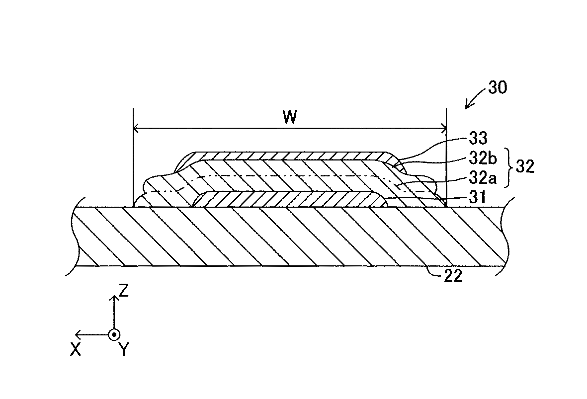
表1に示すように、加熱・真空処理を実行しない場合(NO1)、及び、65℃で加熱・真空処理を実行した場合(NO4)においては、圧電体膜32に絶縁破壊が発生していて、圧電体膜32内に気泡が残留していたことが判る。一方、50℃で加熱・真空処理を実行した場合(NO2,NO3)においては、圧電体膜32に絶縁破壊が発生しておらず、圧電体膜32内の脱泡が確実に行われていたことが判る。
【0056】
以上、説明したように、本発明の実施形態に係る膜形成方法によれば、一枚の圧電体膜32を作製する際、先ず、その前駆膜である一次圧電体膜32aを形成し、前記加熱・真空処理を行って同一次圧電体膜32aの脱泡、及びレベリングを行った後に前記乾燥処理を行って同一次圧電体膜32aを乾燥させる。次いで、一次圧電体膜32aの上面に重ねて、圧電体膜32の前駆膜である二次圧電体膜32bを形成し、前記加熱・真空処理を再び行って同二次圧電体膜32bの脱泡、及びレベリングを行った後に前記乾燥処理を再び行って同二次圧電体膜32bを乾燥させる。従って、一次圧電体膜32a及び二次圧電体膜32bの2枚の前駆膜が積み重ねられてなる一枚の圧電体膜32内に内包されている気泡が効果的に除去され得るとともに、同圧電体膜32のレベリングが確実に達成された。
【0057】
また、一次圧電体膜32a及び二次圧電体膜32bの2枚の膜が積み重ねられて一枚の圧電体膜32が形成(完成)されることから、一次圧電体膜32a及び二次圧電体膜32bの各々の膜厚は、同圧電体膜32の膜厚よりも当然に薄くなる。従って、一枚の膜(一層の膜)で同一の膜厚の圧電体膜32を形成する場合に比して、圧電体膜32の脱泡の程度が向上するとともに、同圧電体膜32の外周部の形状のばらつきの程度が小さくなった。
【0058】
また、乾燥処理後の一次圧電体膜32aに対する二次圧電体膜32b(第2のペースト)の濡れの程度(濡れ性)は、酸化ジルコニウムから成る前記薄肉シート22に対する一次圧電体膜32a(第1のペースト)の濡れの程度(濡れ性)に比して小さいことから、上面視にて(Z軸正方向から見て)二次圧電体膜32bの外周部が一次圧電体膜32aの外周部の外側にはみ出す部分が存在しない。従って、より一層、完成後の圧電体膜32の外周部の形状のばらつきの程度が小さくなった。
【0059】
本発明は上記実施形態に限定されることはなく、本発明の範囲内において種々の変形例を採用することができる。例えば、上記実施形態においては、上述した圧電/電歪素子30の製造工程における工程1にて作製した圧電体ペーストの粘度と工程5にて作製した圧電体ペーストの粘度とを等しくしているが、工程5にて作製した圧電体ペーストの粘度を工程1にて作製した圧電体ペーストの粘度よりも低く設定してもよい。この場合、工程5にて作製する圧電体ペースト全体に対する有機溶剤の(質量)割合を工程1にて作製する圧電体ペースト全体に対する有機溶剤の(質量)割合よりも大きく設定すればよい。これによれば、一次圧電体膜32aを形成するための圧電体ペーストの粘度を比較的高い値に設定することで同一次圧電体膜32aの膜厚を比較的大きく設定し易くなる。更に、二次圧電体膜32bを形成するための圧電体ペーストの粘度を比較的低い値に設定することで二次圧電体膜32bのレベリング、従って、一枚の圧電体膜32全体としてのレベリングが確実に達成され易くなる。即ち、レベリングを確実に達成しつつ厚い圧電体膜32を形成することができる。
【0060】
また、上記実施形態においては、膜形成手法としてスクリーン印刷を用いて圧電体膜を形成しているが、ディッピング、塗布等の公知の他の厚膜形成手法を用いて圧電体膜を形成してもよい。また、上記実施形態においては、2枚の前駆膜(一次圧電体膜32a及び二次圧電体膜32b)を積み重ねて圧電体膜32を形成しているが、3枚以上の前駆膜を積み重ねて圧電体膜を形成してもよい。また、上記実施形態においては、本発明に係る膜形成方法を圧電体膜32にのみ適用しているが、本発明に係る膜形成方法を、下部電極31用の下部電極膜、及び/又は、上部電極33用の上部電極膜に適用してもよい。
【0061】
また、上記実施形態においては、圧電/電歪素子30は、本発明による膜形成方法を適用して作製した1層の圧電体膜32が下部電極31と上部電極33とにより挟まれた構造を有しているが、本発明による膜形成方法を適用して作製した複数層の圧電体膜と複数層の電極とを交互に多層にわたり積み重ねてなる構造を有するように構成してもよい。
【0062】
図10は、本発明の実施形態の変形例に係る膜形成方法を用いて作製した2層の圧電体膜を含む圧電/電歪素子を使用した圧電/電歪ユニットを図3(B)が示す断面と同一の断面にて示した図である。図10において、図3(B)における各構成と対応する構成については、図3(B)における符号と同一の符号を付している。
【0063】
図10に示すように、この変形例では、薄肉シート22の上面に、上記実施形態と同様に下部電極31、圧電体膜32、及び(上記実施形態における上部電極33に相当する)中間電極33をこの順に積み重ねた後、更にその上面に、圧電体膜34、及び上部電極35をこの順に積み重ねて2層の圧電体膜を含む圧電/電歪素子30を作製している。圧電体膜32及び圧電体膜34は、共に、2枚の前駆膜を積み重ねることにより作製している。
【0064】
より具体的に述べると、先ず、上述の実施形態と同様、下部電極31用の下部電極膜を薄肉シート22の上面にスクリーン印刷後、同下部電極膜を乾燥、焼成して下部電極31を作製する。次に、前述の工程1〜9と同一の各工程を順に実行することで2枚の前駆膜を積み重ねて成る圧電体膜32を下部電極31の上面に作製する。次いで、中間電極33用の中間電極膜を圧電体膜32の上面にスクリーン印刷後、同中間電極膜を乾燥、焼成して中間電極33を作製する。
【0065】
続いて、前述の工程1〜9と同一の各工程を順に再び実行することで2枚の前駆膜を積み重ねて成る圧電体膜34を中間電極33の上面に作製する。最後に、上部電極35用の上部電極膜を圧電体膜34の上面にスクリーン印刷後、同上部電極膜を乾燥、焼成して上部電極35を作製する。
【0066】
ここで、下部電極31は、圧電体膜32、及び圧電体膜34の形成前に形成されることから、圧電体膜32の焼成温度と圧電体膜34の焼成温度のうち高い方の温度と同等、若しくはそれ以上の温度に対する耐熱性を有する白金を主成分とする材料から成っていることが好ましい。また、中間電極33は、圧電体膜34の形成前に形成されることから、圧電体膜34の焼成温度と同等、若しくはそれ以上の温度に対する耐熱性を有する白金を主成分とする材料から成っていることが好ましい。一方、上部電極35は、圧電体膜32、及び圧電体膜34の形成後に形成されることから、圧電体膜32の焼成温度と圧電体膜34の焼成温度のうち低い方の温度より低い温度で形成可能な金を主成分とする材料から成っていることが好ましい。
【0067】
なお、図10に示された薄肉シート22のZ軸方向の変形は、圧電/電歪素子30の前記各構成部品31〜35が順に焼成により作製されていく過程において発生するものであって、この変形形状は、上部電極35が作製された後(従って、圧電/電歪素子30全体が完成した後)の段階における形状である。ただし、薄肉シート22は、前記各構成部品31〜35の焼成前の段階から図10に示すようにZ軸方向に変形していてもよい。
【図面の簡単な説明】
【図1】 本発明の実施形態に係る膜形成方法を用いて作製した圧電体膜を含む圧電/電歪素子を使用した圧電/電歪ユニットの平面図である。
【図2】 図1の1−1線に沿った平面にて圧電/電歪ユニットを切断した断面図である。
【図3】 図3(A)は図1に示した圧電/電歪素子の平面図、図3(B)は図3(A)の2−2線に沿った平面にて圧電/電歪素子及び薄肉シートを切断した断面図、図3(C)は図3(A)の3−3線に沿った平面にて圧電/電歪素子及び薄肉シートを切断した断面図である。
【図4】 図1に示した圧電/電歪素子における下部電極を作製した後の状態を示す工程図である。
【図5】 図1に示した圧電/電歪素子における圧電体膜を作製する際の過程の前半部(圧電体膜の前駆膜である一次圧電体膜を作製する際の過程)を示す工程図である。
【図6】 図1に示した圧電/電歪素子における圧電体膜を作製する際の過程の後半部(圧電体膜の前駆膜である二次圧電体膜を作製する際の過程)を示す工程図である。
【図7】 図1に示した圧電/電歪素子における上部電極を作製した後の状態(即ち、完成後の圧電/電歪素子)を示す工程図である。
【図8】 図1に示した圧電/電歪素子における圧電体膜を作製する際の過程の一部である加熱・真空処理を行うための加熱真空装置の部分断面図を含む正面図である。
【図9】 図1に示した圧電/電歪素子における圧電体膜の前駆体である圧電体ペーストの温度を変更した場合の各温度に対する同圧電体ペーストの粘度を測定した結果を示したグラフである。
【図10】 本発明の実施形態の変形例に係る膜形成方法を用いて作製した圧電体膜を含む圧電/電歪素子を使用した圧電/電歪ユニットの断面図である。
【図11】 図11(a)は、ワークの表面上に、(X軸方向の)一辺の長さ(幅)がWmaskの直方体状の比較的膜厚の大きい膜を大気中にて一回スクリーン印刷した直後における膜の平面図、図11(b)は、図11(a)の4−4線に沿った平面でワーク、及び膜を切断した断面図である。
【図12】 図12(a)は、図11に示した膜を、印刷後の所定時間に渡って加熱するとともに略真空にさらした後の時点における膜の平面図、図12(b)は、図12(a)の4−4線に沿った平面でワーク、及び膜を切断した断面図である。
【符号の説明】
10…圧電/電歪ユニット、20…基体部、22…薄肉シート、30…圧電/電歪素子、31…下部電極、32…圧電体膜、32a…一次圧電体膜、32b…二次圧電体膜、33…上部電極、40…加熱真空装置[0001]
BACKGROUND OF THE INVENTION
The present invention relates to a film forming method in which a film having a predetermined pattern is formed on a surface of a film forming body using a film forming method, and more particularly to a film forming method using a thick film forming method such as screen printing.
[0002]
[Prior art]
Conventionally, when a film having a predetermined pattern is formed on the surface of a film forming body (work) using a thick film forming method such as screen printing, a bubble should not be included in the completed film. And, it is required that the surface (upper surface) of the completed film is flat.
[0003]
In order to prevent bubbles from being encapsulated in the completed film, the screen printing apparatus described in Non-Patent
[0004]
According to this, even when bubbles are encapsulated in the paste at the time of production, such as by producing the paste in the atmosphere, etc., at the time before the start of screen printing by exposing the paste (surface) to a substantially vacuum Bubbles encapsulated in the paste can be removed (hereinafter, removing the bubbles may be referred to as “defoaming”), and the paste is completely defoamed before the start of screen printing. Even if it is not, since the paste (surface) continues to be exposed to a substantially vacuum over the time after the end of the screen printing after that point, it is included in the middle of the screen printing process. Air bubbles can be completely removed. Further, since the paste (the surface thereof) continues to be exposed to a substantially vacuum during the screen printing process, no new bubbles are mixed into the paste during the screen printing process. Therefore, it is possible to reliably achieve that bubbles are not included in the completed film.
[0005]
[Non-Patent Document 1]
New Long Seimitsu Kogyo Co., Ltd. vacuum screen printer
LS-340VC catalog (May 27, 2002 1st edition issued)
[0006]
[Problems to be solved by the invention]
However, since the above conventional vacuum screen printing apparatus executes screen printing in a vacuum chamber, it has a relatively large structure such as a squeegee part itself necessary for executing screen printing and a table part itself for setting a work. The body needs to be placed in a vacuum chamber. Therefore, the volume of the vacuum chamber is increased. As a result, there is a problem that the time required for reducing the pressure in the vacuum chamber from atmospheric pressure to a pressure substantially equivalent to vacuum becomes longer and the entire printing apparatus becomes larger.
[0007]
Moreover, when the paste (surface) is exposed to a substantially vacuum, the boiling point of the organic solvent contained in the paste is lowered to adjust the viscosity of the paste, and the organic solvent is likely to evaporate. It becomes easy to change (rise) within a short time. Therefore, in addition to the need to shorten the paste replacement cycle, in the case of screen printing a plurality of times in the same pattern making process in the middle of a single screen printing process or multiple times in succession There is a high possibility that the viscosity of the paste changes (increases) between each screen printing process, and it is difficult to control the quality of the printed film (for example, the film thickness) uniformly.
[0008]
In addition, when screen printing a predetermined pattern film by extruding a predetermined paste from the opening of the mesh-shaped plate making with a squeegee, the surface of the film immediately after printing has irregularities (mesh traces) corresponding to the mesh pattern. Is inevitably formed. When the paste (film) is exposed to the atmosphere, the unevenness is eliminated within a short time by the paste flowing due to the action of gravity acting on the paste itself. As a result, the paste (film) The surface can be flattened (hereinafter, the surface (upper surface) of the membrane being flattened by the action of gravity may be referred to as “leveling”). However, when screen printing is performed using the above-described vacuum screen printing apparatus, there is a period in which a state in which the paste (film) is exposed to a substantially vacuum immediately after printing and the organic solvent easily evaporates continues. Therefore, there is a problem that leveling cannot be reliably achieved by forming a dry film on the paste surface during the period and curing the surface.
[0009]
On the other hand, in order to solve the various problems as described above, a film having a predetermined pattern is screen-printed on a work using a paste in the atmosphere, and the paste (film) is heated for a predetermined time and then substantially omitted. Techniques for exposure to vacuum are also known. According to this, the paste is exposed to a substantially vacuum, and the fluidity of the paste is improved due to a decrease in the viscosity of the paste due to heating. Air bubbles and bubbles newly mixed in the paste when the paste is printed on the workpiece during the screen printing process (and thus all bubbles contained in the paste) can be removed. Moreover, leveling can be more reliably achieved by improving the fluidity of the paste due to a decrease in the viscosity of the paste.
[0010]
However, in this technique, there is a problem that the degree of defoaming of the paste decreases as the film thickness of the printed paste (film) increases, and the degree of variation in the shape of the outer peripheral portion of the film increases. This point will be described below with reference to FIGS. 11 and 12.
[0011]
FIG. 11A shows that the length (width) of one side (in the X-axis direction) on the surface of the
[0012]
FIG. 12 (a) is a plan view of the
[0013]
Further, regarding the defoaming of the paste, the
[0014]
Further, at this time, as shown in FIGS. 12A and 12B, the outer peripheral portion of the
[0015]
As shown in FIG. 12A, the spread amount inevitably varies depending on the position of the outer peripheral portion of the
[0016]
Accordingly, an object of the present invention is formed in a film forming method in which a film having a predetermined pattern is formed on a surface of a film forming body by a film forming method (particularly, a thick film forming method such as screen printing). Regardless of the thickness of the film, the degree of deaeration of the film can be kept high, the degree of variation in the shape of the outer periphery of the film can be reduced, and leveling on the film surface can be reliably achieved. It is to provide.
[0017]
SUMMARY OF THE INVENTION
In the film forming method of the present invention, a precursor film having a predetermined pattern is formed on the surface of the film-forming body using a first paste at a first temperature and a first pressure, and then the precursor film is formed. A first step of removing bubbles contained in at least the precursor film by exposure to a second temperature higher than the first temperature and a second pressure lower than the first pressure; After the new precursor film having the predetermined pattern is overlaid on the surface of the precursor film using the second paste under the first temperature and the first pressure, the new precursor film is formed. Exposing at least a third temperature higher than the first temperature and a third pressure lower than the first pressure to remove bubbles contained in at least the new precursor film. A second step performed at least once, and the predetermined step comprising a plurality of the precursor films Turn (one sheet, one layer of) a method for forming a film.
[0018]
Here, the first paste and the second paste may be the same paste (paste having the same composition (physical properties)). In this case, the first temperature and the first pressure are an atmospheric temperature (normal temperature) and an atmospheric pressure (normal pressure), respectively, and the second temperature and the third temperature are heating. It is preferable that the second pressure and the third pressure are pressures achieved using a vacuum pump (for example, a pressure substantially equivalent to a vacuum). Further, the second temperature and the third temperature may be the same temperature, and the second pressure and the third pressure may be the same pressure. Furthermore, in the first step, the precursor film is exposed to the second temperature and the second pressure to remove bubbles contained in the precursor film, and then the precursor film is dried. Is preferred. Similarly, in the second step, the precursor film is exposed to the third temperature and the third pressure to remove bubbles contained in the precursor film, and then the precursor film is dried. Is preferred.
[0019]
According to this, each time a plurality of precursor films are formed by a predetermined film formation technique (for example, screen printing) at a first temperature and a first pressure (for example, in the atmosphere), The formed precursor film (the precursor film positioned at the top of the stacked precursor films at that time) is then heated to a second (or third) temperature higher than the first temperature (for example, atmospheric air). And a second (or third) pressure lower than the first pressure (e.g., a pressure substantially equivalent to a vacuum). Therefore, as described above, the precursor film is exposed to the second (or third) pressure, and the precursor film is exposed to the second (or third) temperature. In combination with the improvement of the fluidity of the (first and second pastes), each time the precursor film is formed, the precursor film (precursor film located at the uppermost stage) formed in the same is formed. The encapsulated bubbles are removed. In addition, since the flowability of the precursor film is improved, leveling of the formed precursor film (precursor film located at the uppermost stage) is reliably achieved each time the precursor film is formed. The leveling of the (single) membrane can also be achieved reliably.
[0020]
In addition, since a plurality of precursor films of a predetermined pattern are stacked to form (complete) a film of the same pattern including the plurality of precursor films, each film of the precursor film The thickness is naturally smaller than the film thickness of the completed film. Accordingly, as described above, the degree of defoaming of each precursor film is improved, and the degree of variation in the shape of the outer peripheral portion of each precursor film is reduced. As a result, when a (single) film (finished film) having a predetermined film thickness is formed by stacking a plurality of precursor films as in the above method, a single film (single film) is used. Compared to the case of forming a film having the same film thickness, the degree of defoaming of the film (as a whole (single film) after completion) is improved and the shape of the outer periphery of the film is not uniform. The degree of becomes smaller. In other words, regardless of the thickness of the completed film, the degree of defoaming of the film can be maintained high, and the degree of variation in the shape of the outer peripheral portion of the film can be reduced.
[0021]
Also, the above film forming methodIn the first step, the degree of wetness of the first paste with respect to the film forming body in the first step is the second degree with respect to the precursor film (preferably, the precursor film after being dried) in the second step. Than the degree of paste wetnesslarge.According to this, the spread amount of the precursor film located on the lowermost stage formed on the surface (upper surface) of the film forming body among the stacked precursor films is the single number formed on the upper stage, Or it becomes larger than the spread amount of a plurality of precursor films. Therefore, the outer peripheral portion of the precursor film other than the precursor film positioned at the lowermost stage when viewed from the upper side of the film does not exist outside the outer peripheral portion of the precursor film positioned at the lowermost stage, and the outer peripheral portion of the film is further increased. The degree of variation in the shape of each can be reduced.
[0022]
In addition, the film forming methodIn, the viscosity of the second paste used in the second step is under the same temperature as the viscosity of the first paste used in the first stepLow.According to this, by setting the viscosity of the first paste for forming the precursor film located at the lowermost stage to a relatively high value, the film thickness of the precursor film located at the lowermost stage is set to be relatively large. It becomes easy. Further, by setting the viscosity of the second paste for forming a precursor film other than the precursor film positioned at the lowermost level to a relatively low value, the leveling of the precursor film positioned at the uppermost level, and thus the completed film Leveling is surely easily achieved. In other words, a thick (single) film can be formed while reliably achieving leveling.
[0023]
DETAILED DESCRIPTION OF THE INVENTION
Hereinafter, an embodiment of the piezoelectric /
[0024]
The
[0025]
The piezoelectric /
[0026]
The
[0027]
Further, as shown in FIG. 1, the piezoelectric /
[0028]
The
[0029]
The
[0030]
The material of the
[0031]
Next, the manufacturing process of the piezoelectric /
[0032]
First, the
[0033]
Next, a piezoelectric body composed of two (two layers) precursor films at predetermined locations on the upper surface of the
[0034]
Step 1: Material mainly composed of lead zirconate titanate (PZT) with a predetermined particle size (PbZrO)Three-PbTiOThree-Pb (Mg1 / 3 Nb2 / 3) OThree), An organic binder mainly composed of polyvinyl butyral, and an organic solvent that is a mixture of α-terpineol and 2-ethylhexanol in the air at a predetermined ratio, and kneaded in a tri-roll mill. A piezoelectric paste (first paste) that is a precursor of the
[0035]
Step 2: Using this piezoelectric paste, as shown in FIG. 5 (a), the primary
[0036]
Step 3: Heating / vacuum processing is performed on the
[0037]
Next, the heating / vacuum treatment will be specifically described. First, the
[0038]
In this state, the width (length along the X axis) of the primary
[0039]
Step 4: The primary
[0040]
Step 5: In the same manner as in the
[0041]
Step 6: Using this piezoelectric paste, the secondary
[0042]
Step 7: The heating / vacuum process similar to the above-described Step 3 is performed on the
[0043]
In this state, the width (the length along the X axis) of the secondary
[0044]
Step 8: The secondary
[0045]
Step 9: In this way, the piezoelectric film 32 (actually, the
In this way, as shown in FIG. 6B, one (one layer)
[0046]
Next, the
[0047]
Next, FIG. 9 shows the grounds for setting the surface temperature of the table 41a to 50 ° C. in the heating / vacuum treatment performed in the steps 3 and 7 in the manufacturing process of the piezoelectric /
[0048]
The viscosity of the piezoelectric paste with respect to each temperature is measured by repeatedly performing the same process as the heating / vacuum process while sequentially changing the surface temperature of the table 41a. The specific measurement method is as follows.
1; The surface temperature of the table 41a of the
2; Open the
3; Hold for 15 seconds in this state.
4; The
5: Immediately after that, the
6: The surface temperature (predetermined temperature) of the table 41a is appropriately changed, and
[0049]
Specific measurement conditions for measuring the viscosity of the piezoelectric paste are as follows.
Viscometer: B-type viscometer manufactured by Toki Sangyo Co., Ltd.
Corn: R-14
Sample volume: 2.5ml
Shear rate: 0.2 sec-1
[0050]
As shown in FIG. 9, when the surface temperature of the table 41a is lower than about 50 ° C., the viscosity of the piezoelectric paste decreases as the surface temperature (and thus the temperature of the piezoelectric paste) increases (arrows). See A). On the other hand, when the surface temperature of the table 41a is higher than about 50 ° C., the viscosity of the piezoelectric paste increases as the surface temperature (and hence the temperature of the piezoelectric paste) increases (see arrow B). .) That is, when the surface temperature of the table 41a is approximately 50 ° C., the viscosity of the piezoelectric paste is the lowest. This is because, at temperatures exceeding about 50 ° C., the degree of evaporation of the organic solvent in the piezoelectric paste suddenly increases as the temperature increases, and the composition of the piezoelectric paste itself changes greatly. This is based on the fact that the solvent evaporates from the vicinity of the surface of the piezoelectric paste to form a relatively hard (high viscosity) dry film on the surface.
[0051]
On the other hand, in order to remove bubbles contained in the piezoelectric paste, it is preferable that the piezoelectric paste has higher fluidity (and therefore lower viscosity). Therefore, in order to surely defoam the piezoelectric paste, the surface temperature of the table 41a (accordingly, the temperature of the piezoelectric paste) is set within a predetermined range including 50 ° C. (for example, 40 to 60 ° C.). It can be said that it is preferable. The above is the grounds for setting the surface temperature of the table 41a to 50 ° C. in the heating / vacuum processing described above.
[0052]
Next, a test for confirming the effect of performing the heating / vacuum treatment and the effect of setting the surface temperature of the table 41a to 50 ° C. in the heating / vacuum treatment and results thereof will be described. Specifically, a test product of the piezoelectric /
[0053]
The conditions of said NO1-NO4 are as follows.
NO1: The above-described manufacturing process of the piezoelectric /
NO2: The surface temperature of the table 41a is set to 50 ° C. during execution of the heating / vacuum treatment (step 3 or step 7) (therefore, the
NO3: The same condition as NO2.
NO4: The surface temperature of the table 41a during execution of the heating / vacuum treatment (step 3 or step 7) is set to 65 ° C., and
The results of this test are shown in Table 1 below.
[0054]
[Table 1]
As shown in Table 1, when the heating / vacuum treatment is not executed (NO1) and when the heating / vacuum treatment is executed at 65 ° C. (NO4), dielectric breakdown occurs in the
[0056]
As described above, according to the film forming method according to the embodiment of the present invention, when the single
[0057]
In addition, the two films of the primary
[0058]
The degree of wetting (wetting) of the secondary
[0059]
The present invention is not limited to the above embodiment, and various modifications can be employed within the scope of the present invention. For example, in the above embodiment, the viscosity of the piezoelectric paste produced in
[0060]
In the above embodiment, the piezoelectric film is formed by screen printing as the film forming technique. However, the piezoelectric film is formed by using another known thick film forming technique such as dipping or coating. Also good. In the above embodiment, the
[0061]
In the above embodiment, the piezoelectric /
[0062]
FIG. 10 shows a piezoelectric / electrostrictive unit using a piezoelectric / electrostrictive element including a two-layer piezoelectric film manufactured by using a film forming method according to a modification of the embodiment of the present invention. It is the figure shown in the same cross section as the shown cross section. In FIG. 10, components corresponding to those in FIG. 3B are denoted by the same reference numerals as those in FIG.
[0063]
As shown in FIG. 10, in this modification, the
[0064]
More specifically, first, similarly to the above-described embodiment, after the lower electrode film for the
[0065]
Subsequently, the same processes as the above-described
[0066]
Here, since the
[0067]
Note that the deformation in the Z-axis direction of the
[Brief description of the drawings]
FIG. 1 is a plan view of a piezoelectric / electrostrictive unit using a piezoelectric / electrostrictive element including a piezoelectric film manufactured using a film forming method according to an embodiment of the present invention.
2 is a cross-sectional view of a piezoelectric / electrostrictive unit cut along a plane along line 1-1 in FIG.
3A is a plan view of the piezoelectric / electrostrictive element shown in FIG. 1, and FIG. 3B is a plan view along the line 2-2 of FIG. 3A. FIG. 3C is a cross-sectional view of the element and the thin sheet, and FIG. 3C is a cross-sectional view of the piezoelectric / electrostrictive element and the thin sheet cut along a plane 3-3 in FIG.
FIG. 4 is a process diagram showing a state after a lower electrode in the piezoelectric / electrostrictive element shown in FIG. 1 is manufactured.
5 is a diagram showing a first half of a process for manufacturing a piezoelectric film in the piezoelectric / electrostrictive element shown in FIG. 1 (process for manufacturing a primary piezoelectric film that is a precursor film of a piezoelectric film). FIG.
6 shows the latter half of the process for producing a piezoelectric film in the piezoelectric / electrostrictive element shown in FIG. 1 (process for producing a secondary piezoelectric film as a precursor film of the piezoelectric film). It is process drawing.
7 is a process diagram showing a state after an upper electrode is manufactured in the piezoelectric / electrostrictive element shown in FIG. 1 (that is, a completed piezoelectric / electrostrictive element). FIG.
8 is a front view including a partial cross-sectional view of a heating vacuum apparatus for performing a heating / vacuum process, which is a part of a process for producing a piezoelectric film in the piezoelectric / electrostrictive element shown in FIG. 1; .
9 is a graph showing the results of measuring the viscosity of the piezoelectric paste for each temperature when the temperature of the piezoelectric paste, which is the precursor of the piezoelectric film in the piezoelectric / electrostrictive element shown in FIG. 1, is changed. It is.
FIG. 10 is a cross-sectional view of a piezoelectric / electrostrictive unit using a piezoelectric / electrostrictive element including a piezoelectric film manufactured using a film forming method according to a modification of the embodiment of the present invention.
FIG. 11 (a) is a drawing showing a rectangular parallelepiped film having a relatively long thickness (width in one side in the X-axis direction) of Wmask (on the X-axis direction) once on the surface of the workpiece in the atmosphere. FIG. 11B is a cross-sectional view of the work and the film cut along a plane along line 4-4 in FIG. 11A.
FIG. 12 (a) is a plan view of the film after heating the film shown in FIG. 11 for a predetermined time after printing and exposing it to a substantially vacuum, and FIG. 12 (b) is a plan view of the film. It is sectional drawing which cut | disconnected the workpiece | work and the film | membrane in the plane along 4-4 line of Fig.12 (a).
[Explanation of symbols]
DESCRIPTION OF
Claims (3)
前記第1行程の後において、前記第1の温度、且つ前記第1の圧力下にて前記前駆膜の表面上に第2のペーストを用いて前記所定のパターンの新たな前駆膜を重ねて形成した後、前記新たな前駆膜を前記第1の温度よりも高い第3の温度、且つ前記第1の圧力よりも低い第3の圧力下にさらすことで少なくとも同新たな前駆膜内に内包されている気泡を除去する工程を1回以上行う第2工程と、
を備え、複数枚の前記前駆膜から成る前記所定のパターンの膜を形成する膜形成方法において、
前記第1工程における前記被膜形成体に対する前記第1のペーストの濡れの程度は、前記第2工程における前記前駆膜に対する前記第2のペーストの濡れの程度よりも大きく、
前記第2工程において使用される前記第2のペーストの粘度は、前記第1工程において使用される前記第1のペーストの粘度よりも同一温度下において低いことを特徴とする、膜形成方法。 After forming a precursor film having a predetermined pattern using a first paste on the surface of the film forming body at a first temperature and under a first pressure, the precursor film is higher than the first temperature. A first step of removing bubbles contained in at least the precursor film by exposing to a second temperature and a second pressure lower than the first pressure;
After the first step, a new precursor film having a predetermined pattern is formed by using a second paste on the surface of the precursor film at the first temperature and the first pressure. Then, by exposing the new precursor film to a third temperature higher than the first temperature and a third pressure lower than the first pressure, at least the new precursor film is included in the new precursor film. A second step of performing the step of removing the air bubbles at least once;
In a film forming method for forming a film of the predetermined pattern composed of a plurality of the precursor films ,
The degree of wetting of the first paste with respect to the film forming body in the first step is greater than the degree of wetting of the second paste with respect to the precursor film in the second step,
The film forming method according to claim 1, wherein the viscosity of the second paste used in the second step is lower than the viscosity of the first paste used in the first step under the same temperature.
前記第1の温度、及び第1の圧力は、それぞれ、大気温度、及び大気圧力であり、前記第2の温度、及び前記第3の温度は加熱により達成される温度であるとともに、前記第2の圧力、及び前記第3の圧力は真空ポンプを利用して達成される圧力である膜形成方法。The film forming method according to claim 1 ,
The first temperature and the first pressure are an atmospheric temperature and an atmospheric pressure, respectively. The second temperature and the third temperature are temperatures achieved by heating, and the second temperature. And the third pressure is a film forming method achieved by using a vacuum pump.
前記第2行程の後において、未だ焼成されていない前記複数枚の前記前駆膜から成る前記所定のパターンの膜を、前記第2の温度、及び前記第3の温度よりも高い温度で焼成する第3行程を備えた膜形成方法。 After the second step, a film having the predetermined pattern composed of the plurality of precursor films that has not yet been fired is fired at a temperature higher than the second temperature and the third temperature. A film forming method comprising three steps.
Priority Applications (1)
| Application Number | Priority Date | Filing Date | Title |
|---|---|---|---|
| JP2003125617A JP4471585B2 (en) | 2003-04-30 | 2003-04-30 | Film formation method |
Applications Claiming Priority (1)
| Application Number | Priority Date | Filing Date | Title |
|---|---|---|---|
| JP2003125617A JP4471585B2 (en) | 2003-04-30 | 2003-04-30 | Film formation method |
Publications (2)
| Publication Number | Publication Date |
|---|---|
| JP2004335545A JP2004335545A (en) | 2004-11-25 |
| JP4471585B2 true JP4471585B2 (en) | 2010-06-02 |
Family
ID=33502831
Family Applications (1)
| Application Number | Title | Priority Date | Filing Date |
|---|---|---|---|
| JP2003125617A Expired - Fee Related JP4471585B2 (en) | 2003-04-30 | 2003-04-30 | Film formation method |
Country Status (1)
| Country | Link |
|---|---|
| JP (1) | JP4471585B2 (en) |
Families Citing this family (2)
| Publication number | Priority date | Publication date | Assignee | Title |
|---|---|---|---|---|
| JP5128981B2 (en) * | 2007-07-25 | 2013-01-23 | 日本碍子株式会社 | Piezoelectric / electrostrictive actuator and method for manufacturing piezoelectric / electrostrictive actuator |
| JP2020120325A (en) * | 2019-01-25 | 2020-08-06 | 株式会社アルバック | Manufacturing method of ultrasonic probe, and ultrasonic probe |
-
2003
- 2003-04-30 JP JP2003125617A patent/JP4471585B2/en not_active Expired - Fee Related
Also Published As
| Publication number | Publication date |
|---|---|
| JP2004335545A (en) | 2004-11-25 |
Similar Documents
| Publication | Publication Date | Title |
|---|---|---|
| US6411012B2 (en) | Multilayer piezoelectric element and method of producing the same | |
| JP5506009B2 (en) | Piezoelectric element, method for manufacturing the same, diaphragm, and vibration wave drive device | |
| JP4471585B2 (en) | Film formation method | |
| JP2011159839A (en) | Printing method for conduction electrode | |
| JP4807597B2 (en) | Electronic component and manufacturing method thereof | |
| JP4485140B2 (en) | Piezoelectric actuator and manufacturing method thereof | |
| JP2003261397A (en) | Ceramic substrate and manufacturing method thereof and method of manufacturing electronic part using ceramic substrate | |
| JP4183020B2 (en) | Electronic component and manufacturing method thereof | |
| JP3412090B2 (en) | Manufacturing method of laminated piezoelectric body and product thereof | |
| CN1973384A (en) | Multilayer electronic component and injection system using same | |
| JP2951498B2 (en) | Method of manufacturing inkjet head | |
| JP4868707B2 (en) | Multilayer piezoelectric element and injection device | |
| JP4766827B2 (en) | Method for manufacturing piezoelectric laminate | |
| JP2005154207A (en) | Green sheet, laminate formed body, laminate substrate, and method of manufacturing the same | |
| JP4579636B2 (en) | Manufacturing method of gas sensor | |
| JP4350630B2 (en) | Manufacturing method of gas sensor | |
| JP5071253B2 (en) | Manufacturing method of ceramic heater | |
| JP4166404B2 (en) | Gas sensor element and gas sensor including the same | |
| KR100808902B1 (en) | Manufacturing method of ink jet head | |
| JPH056836A (en) | Manufacture of laminated capacitor and dielectric paste used for it | |
| JP3396494B2 (en) | Method of manufacturing ceramic substrate with through hole | |
| JP2011066343A (en) | Liquid spray head, liquid spray device, and piezoelectric element | |
| JPS6362280A (en) | Laminated piezoelectric element and manufacture thereof | |
| JP2004330724A (en) | Piezoelectric element actuator and its manufacturing method | |
| JP2004063351A (en) | Ceramic heater and gas sensor element using the same |
Legal Events
| Date | Code | Title | Description |
|---|---|---|---|
| A621 | Written request for application examination |
Free format text: JAPANESE INTERMEDIATE CODE: A621 Effective date: 20060223 |
|
| A977 | Report on retrieval |
Free format text: JAPANESE INTERMEDIATE CODE: A971007 Effective date: 20091022 |
|
| A131 | Notification of reasons for refusal |
Free format text: JAPANESE INTERMEDIATE CODE: A131 Effective date: 20091027 |
|
| A521 | Request for written amendment filed |
Free format text: JAPANESE INTERMEDIATE CODE: A523 Effective date: 20091225 |
|
| TRDD | Decision of grant or rejection written | ||
| A01 | Written decision to grant a patent or to grant a registration (utility model) |
Free format text: JAPANESE INTERMEDIATE CODE: A01 Effective date: 20100302 |
|
| A01 | Written decision to grant a patent or to grant a registration (utility model) |
Free format text: JAPANESE INTERMEDIATE CODE: A01 |
|
| A61 | First payment of annual fees (during grant procedure) |
Free format text: JAPANESE INTERMEDIATE CODE: A61 Effective date: 20100302 |
|
| FPAY | Renewal fee payment (event date is renewal date of database) |
Free format text: PAYMENT UNTIL: 20130312 Year of fee payment: 3 |
|
| R150 | Certificate of patent or registration of utility model |
Free format text: JAPANESE INTERMEDIATE CODE: R150 |
|
| FPAY | Renewal fee payment (event date is renewal date of database) |
Free format text: PAYMENT UNTIL: 20140312 Year of fee payment: 4 |
|
| LAPS | Cancellation because of no payment of annual fees |