JP4470324B2 - Image signal conversion apparatus and method - Google Patents
Image signal conversion apparatus and method Download PDFInfo
- Publication number
- JP4470324B2 JP4470324B2 JP2000614733A JP2000614733A JP4470324B2 JP 4470324 B2 JP4470324 B2 JP 4470324B2 JP 2000614733 A JP2000614733 A JP 2000614733A JP 2000614733 A JP2000614733 A JP 2000614733A JP 4470324 B2 JP4470324 B2 JP 4470324B2
- Authority
- JP
- Japan
- Prior art keywords
- image signal
- field
- pixel
- class
- output
- Prior art date
- Legal status (The legal status is an assumption and is not a legal conclusion. Google has not performed a legal analysis and makes no representation as to the accuracy of the status listed.)
- Expired - Fee Related
Links
Images


Classifications
-
- H—ELECTRICITY
- H04—ELECTRIC COMMUNICATION TECHNIQUE
- H04N—PICTORIAL COMMUNICATION, e.g. TELEVISION
- H04N7/00—Television systems
- H04N7/01—Conversion of standards, e.g. involving analogue television standards or digital television standards processed at pixel level
- H04N7/0135—Conversion of standards, e.g. involving analogue television standards or digital television standards processed at pixel level involving interpolation processes
- H04N7/0145—Conversion of standards, e.g. involving analogue television standards or digital television standards processed at pixel level involving interpolation processes the interpolation being class adaptive, i.e. it uses the information of class which is determined for a pixel based upon certain characteristics of the neighbouring pixels
Description
技術分野
この発明は、テレビジョン受像機、VTR等に用いて好適な画像信号変換装置および方法に関する。
背景技術
従来、テレビジョン走査方式のフィールド周波数としては、50Hz(PAL方式、SECAM方式等)または60Hz(NTSC方式)が広く採用されている。これらのフィールド周波数の一方を他方に変換するフィールド周波数変換技術が知られている。例えばフィールド周波数を50Hzを60Hzに変換する時には、入力フィールドの5フィールドを出力フィールドの6フィールドに変換することが必要とされる。動きのスムーズな出力画像を得るために、入力画像の動きベクトルを検出し、動きベクトルに基づいて適切な時間情報を有する出力フィールドを形成するようにしていた。
従来のフィールド周波数変換技術は、動きベクトルを検出する必要があり、ハードウエアが大規模になる欠点があった。また、動きベクトル検出の精度は、それほど高くないので、誤検出による画質劣化が生じるおそれがあった。特に、物体の動きに関しては、出力画像中に不自然な動き(ジャーキネスと称される)が発生したり、動画像のエッジのボケが目立つ等の欠点があった。動きベクトルを検出しないで、線形補間によりフィールド数変換を行う方法もあるが、この方法は、動画領域のボケが目立つ欠点がある。
従って、この発明は、従来のフィールド周波数変換技術の欠点を解消することができる画像信号変換装置および方法を提供することにある。
発明の開示
上述した課題を達成するために、請求の範囲1の発明は、入力画像信号のフィールド周波数をM対N(M≠Nで、M,Nは、自然数)の関係で変換する画像信号変換装置において、
出力画像信号の注目フィールドの時間的に最も近傍に位置する入力画像信号のフィールドに含まれる画素を少なくとも含み、出力画像信号の注目フィールド内の注目画素に基づいて決定される入力画像信号の複数の画素に基づいて、注目画素に対するクラスを決定するクラス決定部と、
予め取得された予測情報をクラス毎に記憶するメモリ部と、
出力画像信号の注目フィールドの時間的に最も近傍に位置する入力画像信号のフィールドに含まれる画素を少なくとも含み、出力画像信号の注目フィールド内の注目画素に基づいて決定される入力画像信号の複数の画素を選択する予測画素選択部と、
クラス決定部で決定されたクラスに対応する予測情報と、予測画素選択部で選択された複数の画素とに基づいて、出力画像信号の各注目画素を生成する画素生成部とを有することを特徴とする画像信号変換装置である。
請求の範囲8の発明は、入力画像信号のフィールド周波数をM対N(M≠Nで、M,Nは、自然数)の関係で変換する画像信号変換方法において、
出力画像信号の注目フィールドの時間的に最も近傍に位置する入力画像信号のフィールドに含まれる画素を少なくとも含み、出力画像信号の注目フィールド内の注目画素に基づいて決定される入力画像信号の複数の画素に基づいて、注目画素に対するクラスを決定するクラス決定ステップと、
出力画像信号の注目フィールドの時間的に最も近傍に位置する入力画像信号のフィールドに含まれる画素を少なくとも含み、出力画像信号の注目フィールド内の注目画素に基づいて決定される入力画像信号の複数の画素を選択する予測画素選択スッテプと、
クラス決定ステップで決定されたクラスに対応する予測情報と、予測画素選択ステップで選択された複数の画素とに基づいて、出力画像信号の各注目画素を生成する画素生成ステップとを有することを特徴とする画像信号変換方法である。
この発明によれば、フィールド周波数を変換するのに、クラス分類適応処理を使用している。クラス分類適応処理は、教師画像(フィールド周波数変換処理の時では、出力画像に相当する)と生徒画像(フィールド周波数変換処理の時では、入力画像に相当する)とを使用して、真値と予測値の誤差の自乗和を最小とするような予測係数を定めるものである。従って、動きベクトルを検出しないでも、時間的に変換後のフィールドに相当する画像を生成することができ、動きベクトル検出用の大規模なハードウエアを必要としない利点がある。また、動きベクトル検出の精度が低いことによる画質の劣化を生じない利点がある。さらに、クラス分類適応処理によるフィールド周波数変換処理を行うことにより、フィールド周波数が比較的低いことによる大面積のフリッカーが生じることを防止でき、良好な画像を提示できる。
発明を実施するための最良の形態
以下、この発明の一実施形態について説明する。一実施形態は、フィールド周波数を50Hzから60Hzへ変換するフィールド周波数変換に対してこの発明を適用したものである。この発明では、60Hzの出力画像信号の画素をクラス分類適応処理によって生成する。
クラス分類適応処理は、入力信号である画像信号の時間的および/または空間的特徴に応じてクラス分割を行い、クラス毎に予め学習により獲得された予測係数値を格納した記憶手段を持ち、予測式に基づいた演算により最適な推定値を出力する方式であり、クラス分類適応処理によって、従来のフィールド周波数変換で問題となっていた動きの不自然さを解消できる。
この画素生成装置の一例では、第1図に示すように、入力画像信号(フィールド周波数50Hzのインターレス信号)が領域切り出し部1に供給され、クラス分類および予測演算に必要とされる複数の画素が含まれる領域が切り出される。領域切り出し部1の出力がクラス検出回路2および12、予測タップ選択回路3および13に供給される。クラス検出回路2および12は、作成すべき出力画素の近傍の入力画素のレベル分布のパターンに対応するクラスを検出する。並列に画素生成のための二つの構成を設けるのは、入力画像信号中の1ラインの時間で、出力画像の2ラインを作成するためである。作成される一方のライン情報をMと表記し、その他方のライン情報をSとして表記する。なお、破線で囲んで示す構成は、LSIの構成とされる。
クラス検出回路2および12のそれぞれにより検出されたクラスが予測タップ選択回路3、13と予測係数メモリ4、14とに供給される。予測係数メモリ4、14からは、クラスに対応する予測係数セットが読出され、積和演算回路5、15に読出された予測係数セットが供給される。予測タップ選択回路3、13は、クラスに応じて使用する予測タップを選択する構成とされている。予め各クラスの予測係数を学習によって得る時に、予測係数と使用する予測タップ位置情報との両者を得るようにしている。予測タップ選択回路3、13には、予測タップ位置情報がクラス毎に記憶されたメモリ(図示せず)が設けられている。このメモリからクラスに対応して読出された予測タップ位置情報がタップ切り替え用のセレクタに供給され、セレクタ(図示せず)が選択的に予測タップを出力する。予測タップ選択回路3、13からの予測タップが積和演算回路5、15に供給される。
積和演算回路5、15では、予測タップ(入力画像信号の画素)と予測係数セットとの線形推定式を用いて出力画像信号の画素値を算出する。積和演算回路5、15がそれぞれフィールド周波数が入力画像信号と等しい50Hzの出力画像信号の第1の画素値Mおよび第2の画素値Sを出力する。積和演算回路5からの第1の画素値がフィールドメモリ6に供給され、積和演算回路15からの第2の画素値がフィールドメモリ16に供給される。
フィールドメモリ6、16は、クラス分類適応処理で生成された第1および第2の画素値のフィールド周波数を50Hzから60Hzへ変換する処理(速度変換処理)を行う。フィールドメモリ6、16の出力が60Hzのフィールド毎に切り替えられるセレクタ7に入力される。セレクタ7は、フィールドメモリ6、16のそれぞれの出力を交互に選択し、出力画像信号(フィールド周波数60Hz)を発生する。
図示しないが、出力画像信号がCRTディスプレイに供給される。CRTディスプレイは、フィールド周波数60Hzの出力画像信号を表示することが可能なように、その同期系が構成されている。入力画像信号としては、放送信号、またはVTR等の再生装置の再生信号が供給される。すなわち、この一例をテレビジョン受像機に内蔵することができる。
なお、入力画像信号と出力画像信号とは、フィールド周波数のみならず、水平ライン周波数(ライン数)も相違する場合がある。従って、その場合には、フィールド数の変換と共に、ライン数の変換も必要とされる。ライン数変換も、クラス分類適応処理によって行うことができる。さらに、クラス分類適応処理によって、水平方向の画素数を入力画像信号の2倍とすることもできる。これらの処理を組み合わせることによって、所望の出力画像信号を形成することができる。但し、この発明は、フィールド数の変換に要旨があるので、ライン数、水平方向の画素数についての説明については、省略する。
第2図は、この発明の一実施形態のフィールド変換動作を横軸に時間、縦軸に垂直方向をとって示すものである。但し、垂直方向の画素数(ライン数)は、実際の画素数よりはるかに少ないものに簡略化されている。第2図Aが50Hzのタイムスケールで表された入力画像信号であり、第2図Bが60Hzのタイムスケールで表された出力画像信号である。
第2図Aの入力フィールドf1〜f5の5フィールドが第2図Bの出力フィールドF1〜F6の6フィールドへ変換される。出力フィールドF1は、入力フィールドf1から第1の出力画素Mとして生成される。出力フィールドF2は、入力フィールドf1から第2の出力画素Sとして生成される。出力フィールドF3は、入力フィールドf2から第1の出力画素Mとして生成される。出力フィールドF4は、入力フィールドf3から第2の出力画素Sとして生成される。出力フィールドF5は、入力フィールドf4から第1の出力画素Mとして生成される。出力フィールドF6は、入力フィールドf5から第2の出力画素Sとして生成される。このように、クラス分類適応処理で生成される出力フィールドの基になる入力フィールドは、時間的になるべく近いものである。
第3図は、フィールドメモリ6および16の動作を横軸に時間、縦軸にフィールドメモリ6および16のアドレスをとって示すものであり、また、フィールドメモリ6および16の書き込みアドレスの変化が細線、それらの読み出しアドレスの変化が太線で示されている。第3図Aは、積和演算回路5およびフィールドメモリ6による出力生成動作を示し、第3図Bは、積和演算回路15およびフィールドメモリ16による出力生成動作を示す。第3図中で各フィールドに対して付された参照符号は、第2図中で使用したものと対応している。
第3図Aに示すように、入力フィールドf1から積和演算回路5から出力されるフィールドf1Mがフィールドメモリ6に書き込まれる。若し、後述する例のように、入力フィールドf1と出力フィールドF1の位相とが時間的に全く重なる場合には、積和演算回路5からのフィールドf1Mは、入力フィールドf1と同一の画像とされる。また、第3図Bに示すように、入力フィールドf1から積和演算回路15から出力されるフィールドf1Sがフィールドメモリ16に書き込まれる。これらのフィールドf1Mおよびf1Sは、入力フィールド周波数(50Hz)のタイムスケールで、同一フィールド期間において生成される。フィールドメモリ6からは、出力フィールド周波数(60Hz)のタイムスケールでもって、出力フィールドF1(書き込まれたフィールドf1M)が読み出される。同様に、フィールドメモリ16から出力フィールド周波数のタイムスケールでもって、出力フィールドF2(書き込まれたフィールドf1S)が読み出される。出力フィールドF2は、出力フィールドF1の次のフィールドを構成する。
入力フィールドf2からクラス分類適応処理によりフィールドf2Mが生成され、積和演算回路5からのフィールドf2Mがフィールドメモリ6に書き込まれる。フィールドf2Mが60Hzのタイムスケールで読み出され、出力フィールドF3として出力される。入力フィールドf2の期間では、第3図Bにおいて破線で示すように、フィールドf1Sは、出力フィールドとして使用されないので、フィールドメモリ16に対する書き込みが休止される。次の入力フィールドf3から生成されたフィールドf3Sがフィールドメモリ16に対して書き込まれる。入力フィールドf3の期間では、第3図Aにおいて破線で示すように、フィールドf3Mは、出力フィールドとして使用されないので、フィールドメモリ6に対する書き込みが休止される。フィールドメモリ16から出力フィールドF4が読み出される。
次の入力フィールドf4から生成されたフィールドf4Mがフィールドメモリ6に対して書き込まれる。入力フィールドf4の期間では、第3図Bにおいて破線で示すように、フィールドメモリ16に対する書き込みが休止される。フィールドメモリ6から出力フィールドF5が読み出される。さらに次の入力フィールドf5から生成されたフィールドf5Sがフィールドメモリ16に対して書き込まれる。入力フィールドf5の期間では、第3図Aにおいて破線で示すように、フィールドメモリ6に対する書き込みが休止される。フィールドメモリ16から出力フィールドF6が読み出される。
以上の入力フィールドf1〜f5から出力フィールドF1〜F6をクラス分類適応処理で生成する処理が繰り返される。第3図Aおよび第3図Bから分かるように、フィールドメモリ6および16においては、書き込みアドレスが読み出しアドレスを追い越すことがなく、正常な読み出し出力が発生する。セレクタ7は、出力フィールド毎に交互にフィールドメモリ6の読み出し出力(第3図Aの太線部分)とフィールドメモリ16の読み出し出力(第3図Bの太線部分)の一方を順次選択して出力する。セレクタ7の出力に、50Hzから60Hzへフィールド周波数が変換された出力映像信号が発生する。
なお、第1図に示されるクラス分類適応処理の構成は、コンポーネントカラー画像信号の一つのコンポーネントに対応したものであり、輝度信号、二つの色差信号の計3個のコンポーネントに対して、第1図に示される構成をそれぞれ設けても良い。さらに、コンポーネントカラー画像信号に限らず、コンポジットカラー画像信号に対してもこの発明を適用することができる。
以下、この発明の一実施形態におけるクラス分類適応処理について、より詳細に説明する。クラス分類適応処理の際に設定されるクラスタップおよび予測タップの一例を説明する。最初に、第4図を参照して、クラス分類適応処理のモードの定義を説明する。第4図では、10フィールドでインターレスを考慮したパターンが一巡している。一方、第2図では、5フィールドでパターンが一巡している。インターレス(画素位置)を考慮しないで時間的関係のみに着目する場合には、第2図に示したように、5フィールドでパターンが一巡することになる。
第4図には、50Hzのフィールド周波数の入力画像と60Hzのフィールド周波数の出力画像とが示されている。入力フィールドf1の位相と時間的に重なる出力フィールドF1は、入力フィールドf1と同一の画像が出力される。但し、出力フィールドF1との画像をクラス分類適応処理で生成しても良い。入力フィールドと出力フィールドの時間的関係と、これらの間の垂直方向の画素位置に応じて次のようにモードを定義する。
出力フィールドF1、F2およびF3のように、時間的にもっとも近接する(時間的に重なる場合も含む)入力フィールドと垂直方向の画素位置が同一の場合をモードAと定義する。出力フィールドF5およびF6のように、時間的にもっとも近接する入力フィールドと垂直方向の画素位置が1/2ラインずれた位置の場合をモードBと定義する。出力フィールドF4のように、入力フィールドf3およびf4の時間的中間位置の場合をモードCと定義する。これらのモードを定義するのは、モード毎に予測係数セットを学習により定めるためであり、それによって、予測の精度が向上できる。なお、最も近接する入力フィールドまでの距離の大きさによって、モードを細分化しても良い。但し、この場合では、ハードウエアの規模が増大するので、実施形態では、モードを細分化していない。
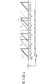
第5図は、モードAにおけるタップ構造を示す。第5図は、縦軸を垂直方向、横軸を時間方向とし、出力フィールド例えばF3のある画素(黒い丸印で示す)を生成する場合の画素位置を概略的に示す。モードAでは、入力フィールドf2、f3、f4に含まれる画素を使用して、出力フィールドF3の画素がクラス分類適応処理によって生成される。すなわち、入力フィールドf2に含まれ、予測しようとする画素と垂直方向で1/2ラインずれた位置の上下の2画素と、入力フィールドf3に含まれ、予測しようとする画素と同一位置の画素と、入力フィールドf4に含まれ、予測しようとする画素と垂直方向で1/2ラインずれた位置の上下の2画素とが使用される。例えば、クラス検出回路2、予測タップ選択回路3、予測係数メモリ4、積和演算回路5によってフィールドF3内の画素が生成される。
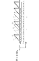
第6図は、モードBにおけるタップ構造を示す。第6図は、縦軸を垂直方向、横軸を時間方向とし、出力フィールド例えばF5のある画素(黒い丸印で示す)を生成する場合の画素位置を概略的に示す。モードBでは、入力フィールドf3、f4、f5に含まれる画素を使用して、出力フィールドF5の画素がクラス分類適応処理によって生成される。すなわち、入力フィールドf3に含まれ、予測しようとする画素と同一位置の画素と、入力フィールドf4に含まれ、予測しようとする画素と垂直方向で1/2ラインずれた位置の上下の2画素と、入力フィールドf5に含まれ、予測しようとする画素と同一位置の画素とが使用される。例えば、クラス検出回路2、予測タップ選択回路3、予測係数メモリ4、積和演算回路5によってフィールドF5内の画素が生成される。
第7図は、モードCにおけるタップ構造を示す。第7図は、縦軸を垂直方向、横軸を時間方向とし、出力フィールド例えばF4のある画素(黒い丸印で示す)を生成する場合の画素位置を概略的に示す。モードCでは、入力フィールドf3、f4に含まれる画素を使用して、出力フィールドF4の画素がクラス分類適応処理によって生成される。すなわち、入力フィールドf3に含まれ、予測しようとする画素と垂直方向で1/2ラインずれた位置の上下の2画素と、入力フィールドf4に含まれ、予測しようとする画素と同一位置の画素とが使用される。例えば、クラス検出回路12、予測タップ選択回路13、予測係数メモリ14、積和演算回路15によってフィールドF4内の画素が生成される。
第5図、第6図および第7図のタップ構造は、クラスタップおよび予測タップとして使用する入力画素と、それらが含まれるフィールドとを示している。クラスタップおよび予測タップは、時間方向および垂直方向のみならず、同一フィールド内の水平方向に広がりを持つことも可能である。また、クラスタップと予測タップとを同一のタップ構造とせずに、両者を異ならせることも可能である。クラスタップおよび予測タップのモードに応じた切り替えは、クラス検出回路2,12および予測タップ選択回路3,13のそれぞれにおいてなされる。領域切り出し回路1は、クラスタップおよび予測タップとして使用される可能性のある全ての入力画素を同時に出力するものである。
クラスタップおよび予測タップを空間的な配置例について説明する。例えば第8図に示すように空間的にも複数の入力画素によって予測タップを構成し、第8図Bに示すように、複数の入力画素によってクラスタップを構成しても良い。第8図Aおよび第8図Bは、縦軸を垂直方向、横軸を水平方向にとって画素の配置を示す。第8図Aに示すように、−1フィールドに含まれ、生成しようとする画素(黒い丸印)と垂直方向で上下の位置の6個の入力画素と、0フィールドに含まれ、生成しようとする画素と上下左右の位置に隣接する4個の入力画素との合計10個の入力画素により予測タップが構成される。
第8図Bに示すように、−1フィールドに含まれ、生成しようとする画素と垂直方向で上下の位置の2画素と、0フィールドに含まれ、生成しようとする画素に対して垂直方向で上下の位置の2画素によってクラスタップが構成される。
クラス検出回路2、12は、クラスタップのレベル分布のパターンを検出する。この場合、クラス数が膨大となることを防ぐために、各画素8ビットの入力データをより少ないビット数のデータへ圧縮するような処理を行う。一例として、ADRC(Adaptive Dynamic Range Coding)によって、クラスタップの入力画素のデータが圧縮される。なお、情報圧縮方式としては、ADRC以外にDPCM(予測符号化)、VQ(ベクトル量子化)等の圧縮方式を用いても良い。
本来、ADRCは、VTR(Video Tape Recoder)向け高能率符号化用に開発された適応的再量子化法であるが、信号レベルの局所的なパターンを短い語長で効率的に表現できるので、この一例では、ADRCをクラス分類のコード発生に使用している。ADRCは、クラスタップのダイナミックレンジをDR、ビット割当をn、クラスタップの画素のデータレベルをL、再量子化コードをQとして、以下の式(1)により、最大値MAXと最小値MINとの間を指定されたビット長で均等に分割して再量子化を行う。
DR=MAX−MIN+1
Q={(L−MIN+0.5)×2/DR} (1)
ただし、{ }は切り捨て処理を意味する。
なお、動きクラスを併用して、クラスと動きクラスとを統合してクラスを検出するようにしても良い。この場合、動きクラスに応じて、クラスタップを切り替えるようにしても良い。動きクラスは、例えばフレーム間差分の大きさに応じて生成されるので、動きベクトルを検出する場合と比較してハードウエアの規模が小さくて良い。
そして、積和演算回路5,15は、予測タップ選択回路3,13でそれぞれ選択された各予測タップ(画素値)と、予測係数メモリ4,14からそれぞれ読み出された各係数との線形1次結合によって、画素値を生成する。線形1次結合に限らず、高次の推定式によって画素値を生成しても良い。この場合、第3図のタイミングチャートに示されるように、予測係数メモリ4には、出力フィールドF3およびF5を生成するために使用する予測係数テーブルが格納され、また、予測係数メモリ14には、出力フィールドF2、F4およびF6を生成するために使用する予測係数テーブルが格納されている。各テーブルは、予測係数セットを、モードとクラス検出回路2,12で決定されたクラスとに対応する個数有する。各テーブル(予測係数)は、予め後述する学習処理によって取得されている。
積和演算回路5は、予測タップ選択回路3、または13からの予測タップ(画素値)x1,x2,・・・xiと、予測係数セットw1,w2,・・・wiとの線形1次結合式(式(2))の演算を行うことにより、画素値を算出する。積和演算回路15は、同様にして画素値を算出する。
L1=w1x1+w2x2+・・・・+wixi (2)
このように、予測係数セットが各クラス毎に予め学習により求められた上で、予測係数メモリ4、14に記憶しておき、入力される予測タップおよび読出された予測係数セットに基づいて演算が行われ、入力されたデータに対応する出力データを形成して出力する。従って、動きベクトル検出を行わずに、フィールド数変換を行うことができる。
予測係数の作成(学習)処理について第9図を用いて説明する。予測係数を学習によって得るためには、フィールド周波数300Hzのプログレッシブの高速動作のビデオカメラにより撮影した画像を使用する。この画像が間引き部31によって、垂直方向で画素数が1/2とされ、フィールド周波数が60Hzのインターレス画像信号(生徒画像)が形成される。また、間引き部41によって、垂直方向で画素数が1/2とされ、フィールド周波数50Hzの画像信号(教師画像)が形成される。間引き部41からの教師画像と間引き部31からの生徒画像とを学習用の対とする。第1図に示す入力画像が生徒画像に対応し、出力画像が教師画像に対応する。学習は、教師画像(真値)と生徒画像との間で、両者の対応する画素の誤差の自乗和を最小とする予測係数を最小自乗法によって求める処理である。
第10図は、予測係数を学習する時の画素構造を示す。縦軸が垂直方向であり、横軸が時間方向である。間引き部31は、フィールド周波数300Hzのプログレッシブ画像を時間方向に1/6に間引くと共に、ライン数を1/2に間引き、フィールド周波数50Hz、インターレス走査の生徒画像を生成する。間引き部41は、フィールド周波数300Hzのプログレッシブ画像を時間方向に1/5に間引くと共に、ライン数を1/2に間引き、フィールド周波数60Hz、インターレス走査の教師画像を生成する。
間引き部31からの生徒画像信号が予測タップ領域切り出し部32およびクラスタップ領域切り出し部33に供給される。クラスタップ領域切り出し部33からのクラスタップがクラス検出回路34および35に供給される。予測タップ領域切り出し部32は、各モードで画素を作成するための予測タップを出力する。クラス検出回路34、35は、モード毎に設定されたクラスタップのデータをADRCにより圧縮し、クラス情報を発生する。これらのクラスタップおよび予測タップは、前述した構造のもの(第4図〜第7図参照)である。
予測タップ領域切り出し部32からの予測タップが正規方程式加算回路36、37に供給される。正規方程式加算回路36、37の説明のために、複数個の入力画素から出力画素への変換式の学習とその予測式を用いた信号変換について述べる。以下に、説明のために、より一般化してn画素による予測を行う場合について説明する。予測タップとして選択される入力画素の信号レベルをそれぞれx1、‥‥、xnとし、教師画像中の出力画素の信号レベルをyとしたとき、クラス毎に予測係数セットw1、‥‥、wnによるnタップの線形推定式を設定する。これを下記の式(3)に示す。学習前は、wiが未定係数である。
y=w1x1+w2x2+‥‥+wnxn (3)
学習は、クラス毎に複数の画像信号に対して行う。データ数がmの場合、式(3)にしたがって、以下に示す式(4)が設定される。
yk=w1xk1+w2xk2+‥‥+wnxkn (4)
(k=1,2,‥‥m)
m>nの場合、予測係数セットwi、‥‥wnは、一意に決まらないので、誤差ベクトルeの要素を以下の式(5)で定義して、式(6)を最小にする予測係数セットを求める。いわゆる、最小自乗法による解決である。
ek=yk−{w1xk1+w2xk2+‥‥+wnxkn} (5)
(k=1,2,‥‥m)
![]()

学習に充分なフレーム数のデータの入力が終了した後、正規方程式加算回路36、37は、予測係数決定部38に正規方程式データを出力する。予測係数決定部38は、正規方程式を掃き出し法等の一般的な行列解法を用いて、wiについて解き、予測係数セットを算出する。予測係数決定部38は、算出された予測係数セットを予測係数メモリ39、40に書込む。
以上のように学習を行った結果、予測係数メモリ39、40のそれぞれには、クラス毎に、出力画像信号の注目画素yを推定するための、もっとも真値に近い推定ができる予測係数セットが格納される。予測係数メモリ39、40に格納された予測係数セットは、上述の画像情報変換装置において、予測係数メモリ4、14にロードされる。
また、予測タップ領域切り出し部32が出力する予測タップの個数は、画素生成装置において使用される予測タップの個数より大きいものとされる。従って、予測係数決定部38は、クラス毎により多くの予測係数が求まる。この求まった予測係数の中で、絶対値が大きいものから順に使用する数の予測係数セットが選択される。選択された予測係数がメモリ39、40のクラスに対応するアドレスにそれぞれ格納される。従って、クラス毎に予測タップが選択されることになり、この予測タップの選択位置情報がクラス毎にメモリ(図示しない)に格納される。このような予測タップ選択処理によって、各クラスに適合した予測タップを選択することが可能となる。
以上の処理により、線形推定式により、フィールド周波数が50Hzのデータからフィールド周波数が60Hzの画像のデータを作成するための予測係数の学習が終了する。
なお、フィールド周波数50Hzから60Hzへのフィールド周波数の変換処理について説明したが、この逆の60Hzから50Hzへのフィールド周波数の変換処理に対しても同様にこの発明を適用できる。また、入力画像信号および出力画像信号のフィールド周波数は、50Hz、60Hzには限定されず、フィールド周波数をM対N(M≠Nで、M,Nは、1でない整数)に変換する場合に対して同様にこの発明を適用できる。例えば48Hzのフィールド周波数の入力画像信号を60Hzのフィールド周波数の画像信号へ変換できる。また、VGA(Video Graphics Array,640x480画素)、XGA(eXtended Graphics Array,1024x768画素)等のコンピュータ画像のフィールド周波数を変換する処理に対してもこの発明を適用することができる。さらに、フィールド周波数の変換に加えて水平方向および/または垂直方向の画素数を2倍とする処理を同時に行うようにしても良い。
第11図は、一実施形態とは逆にフィールド周波数を60Hzから50Hzへ変換する場合の処理を説明するものである。第11図も、第3図と同様に、二つのフィールドメモリの各フィールドメモリの動作を横軸に時間、縦軸にフィールドメモリのアドレスをとって示すものであり、また、フィールドメモリの書き込みアドレスの変化が細線、それらの読み出しアドレスの変化が太線で示されている。
第11図Aに示すように、入力フィールドf1と同一画像のフィールドF1’が一方のフィールドメモリに書き込まれ、50Hzのタイムスケールで出力フィールドF1として読み出される。また、第11図Bに示すように、入力フィールドf2からクラス分類適応処理により生成されたフィールドF2’が他方のフィールドメモリに書き込まれ、フィールドF2として読み出される。フィールドf2の期間では、一方のフィールドメモリに対する書き込みが休止される。
入力フィールドf3からクラス分類適応処理によりフィールドF3’が生成され、フィールドF3’が一方のフィールドメモリに書き込まれる。フィールドF3’が50Hzのタイムスケールで読み出され、出力フィールドF3として出力される。次の入力フィールドf4から生成されたフィールドF4’が他方のフィールドメモリに対して書き込まれる。さらに、入力フィールドf5から生成された出力フィールドF5’が一方のフィールドメモリに書き込まれ、出力フィールドF5として出力される。入力フィールドf5の期間では、第11図Aにおいて破線で示すように、一方のフィールドメモリに対する書き込みが休止される。他方のフィールドメモリにおいては、書き込み動作の休止期間が存在しない。これは、他方のフィールドメモリにおいては、クラス分類に不要な入力フィールドが書き込まれても、その後にクラス分類に使用する入力フィールドによって上書きれるからである。
以上の入力フィールドf1〜f6から出力フィールドF1〜F5をクラス分類適応処理で生成する処理が繰り返される。第11図Aおよび第11図Bから分かるように、各フィールドメモリにおいては、書き込みアドレスが読み出しアドレスを追い越すことがなく、正常な読み出し出力が発生する。そして、一実施形態と同様に、出力フィールド毎に交互に各フィールドメモリの読み出し出力(第11図中の太線部分)を選択することによって、60Hzから50Hzへフィールド周波数が変換された出力映像信号が発生する。
上述したこの発明による画像情報変換装置を例えばCRTディスプレイのような表示装置と入力信号源との間に設けることによって、表示装置のフィールド周波数と入力画像信号のフィールド周波数の不一致の問題を解決することができる。
この発明は、フィールド周波数(フィールド数)の変換をクラス分類適応処理によって行うので、動きベクトルの検出が不要であり、動きベクトル検出のためにハードウエアが大規模となる問題が生じない。また、動きベクトル検出の精度が低いことに起因する画質劣化を生じない。さらに、線形変換でフィールド数変換を行う方法と比して、動画像のボケを生じない利点がある。また、50Hzから60Hzへ入力画像信号のフィールド周波数を変換するように、低いフィールド周波数をより高いフィールド周波数へ変換することによって、大面積フリッカーを取り除くことができる。
【図面の簡単な説明】
第1図は、この発明の一実施形態のブロック図である。
第2図は、一実施形態におけるフィールド周波数変換処理を説明するための略線図である。
第3図は、一実施形態におけるフィールド周波数変換処理におけるフィールドメモリの動作を説明するためのタイミングチャートである。
第4図は、フィールド周波数変換をクラス分類適応処理で行う時のモードの定義を説明するための略線図である。
第5図は、モードAにおけるタップ構造を説明するための略線図である。
第6図は、モードBにおけるタップ構造を説明するための略線図である。
第7図は、モードCにおけるタップ構造を説明するための略線図である。
第8図は、予測タップおよびクラスタップの空間的配置の一例う示す略線図である。
第9図は、予測係数を学習する時の構成を示すブロック図である。
第10図は、予測係数を学習する時に使用する生徒画像と教師画像との関係を示す略線図である。
第11図は、この発明の他の実施形態におけるフィールド周波数変換処理におけるフィールドメモリの動作を説明するためのタイミングチャートである。Technical field
The present invention relates to an image signal conversion apparatus and method suitable for use in a television receiver, a VTR, and the like.
Background art
Conventionally, 50 Hz (PAL system, SECAM system, etc.) or 60 Hz (NTSC system) has been widely adopted as the field frequency of the television scanning system. A field frequency conversion technique for converting one of these field frequencies into the other is known. For example, when converting the field frequency from 50 Hz to 60 Hz, it is necessary to convert 5 fields of the input field to 6 fields of the output field. In order to obtain an output image with smooth motion, a motion vector of the input image is detected, and an output field having appropriate time information is formed based on the motion vector.
The conventional field frequency conversion technique needs to detect a motion vector, and has a drawback that the hardware becomes large-scale. In addition, since the accuracy of motion vector detection is not so high, there is a risk of image quality deterioration due to erroneous detection. In particular, the movement of the object has disadvantages such as an unnatural movement (referred to as jerkiness) in the output image and blurring of the edge of the moving image. There is a method of converting the number of fields by linear interpolation without detecting a motion vector, but this method has a drawback that blur in a moving image region is conspicuous.
Accordingly, it is an object of the present invention to provide an image signal conversion apparatus and method that can eliminate the disadvantages of the conventional field frequency conversion technology.
Disclosure of the invention
In order to achieve the above-described problems, the invention of
A plurality of pixels of the input image signal determined based on the target pixel in the target field of the output image signal, including at least pixels included in the field of the input image signal located closest in time to the target field of the output image signal A class determining unit that determines a class for the target pixel based on the pixel;
A memory unit for storing prediction information acquired in advance for each class;
A plurality of pixels of the input image signal determined based on the target pixel in the target field of the output image signal, including at least pixels included in the field of the input image signal located closest in time to the target field of the output image signal A predictive pixel selector that selects pixels;
A pixel generation unit that generates each pixel of interest of the output image signal based on prediction information corresponding to the class determined by the class determination unit and a plurality of pixels selected by the prediction pixel selection unit; An image signal conversion device.
The invention of
A plurality of pixels of the input image signal determined based on the target pixel in the target field of the output image signal, including at least pixels included in the field of the input image signal located closest in time to the target field of the output image signal A class determining step for determining a class for the pixel of interest based on the pixel;
A plurality of pixels of the input image signal determined based on the target pixel in the target field of the output image signal, including at least pixels included in the field of the input image signal located closest in time to the target field of the output image signal A predictive pixel selection step for selecting pixels;
A pixel generation step of generating each pixel of interest of the output image signal based on prediction information corresponding to the class determined in the class determination step and a plurality of pixels selected in the prediction pixel selection step This is an image signal conversion method.
According to the present invention, the classification adaptation process is used to convert the field frequency. The classification adaptation process uses a teacher image (corresponding to an output image at the time of field frequency conversion processing) and a student image (corresponding to an input image at the time of field frequency conversion processing), A prediction coefficient that minimizes the sum of squares of errors of predicted values is determined. Therefore, an image corresponding to a temporally converted field can be generated without detecting a motion vector, and there is an advantage that a large-scale hardware for detecting a motion vector is not required. Further, there is an advantage that image quality is not deteriorated due to low accuracy of motion vector detection. Furthermore, by performing the field frequency conversion process by the class classification adaptive process, it is possible to prevent a large area flicker due to a relatively low field frequency and to present a good image.
BEST MODE FOR CARRYING OUT THE INVENTION
Hereinafter, an embodiment of the present invention will be described. In one embodiment, the present invention is applied to field frequency conversion for converting a field frequency from 50 Hz to 60 Hz. In the present invention, a pixel of an output image signal of 60 Hz is generated by class classification adaptive processing.
The class classification adaptive processing performs class division according to temporal and / or spatial characteristics of an image signal that is an input signal, and has a storage means that stores a prediction coefficient value obtained by learning in advance for each class, and performs prediction. This is a method of outputting an optimum estimated value by calculation based on the equation, and the unnatural motion that has been a problem in the conventional field frequency conversion can be eliminated by the class classification adaptive processing.
In an example of this pixel generation device, as shown in FIG. 1, an input image signal (interlace signal with a field frequency of 50 Hz) is supplied to the
The classes detected by the
The product-
The
Although not shown, an output image signal is supplied to the CRT display. The CRT display has a synchronous system so that an output image signal with a field frequency of 60 Hz can be displayed. As an input image signal, a broadcast signal or a reproduction signal of a reproduction device such as a VTR is supplied. That is, this example can be incorporated in a television receiver.
Note that the input image signal and the output image signal may differ not only in the field frequency but also in the horizontal line frequency (number of lines). Therefore, in that case, conversion of the number of lines is required together with the conversion of the number of fields. The line number conversion can also be performed by the class classification adaptive process. Furthermore, the number of pixels in the horizontal direction can be made twice that of the input image signal by the class classification adaptive processing. By combining these processes, a desired output image signal can be formed. However, since the present invention has a gist in the conversion of the number of fields, description of the number of lines and the number of pixels in the horizontal direction will be omitted.
FIG. 2 shows the field conversion operation of one embodiment of the present invention with time on the horizontal axis and vertical direction on the vertical axis. However, the number of pixels in the vertical direction (number of lines) is simplified to be much smaller than the actual number of pixels. FIG. 2A is an input image signal represented on a time scale of 50 Hz, and FIG. 2B is an output image signal represented on a time scale of 60 Hz.
5 fields of input fields f1 to f5 in FIG. 2A are converted into 6 fields of output fields F1 to F6 in FIG. 2B. The output field F1 is generated as the first output pixel M from the input field f1. The output field F2 is generated as the second output pixel S from the input field f1. The output field F3 is generated as the first output pixel M from the input field f2. The output field F4 is generated as the second output pixel S from the input field f3. The output field F5 is generated as the first output pixel M from the input field f4. The output field F6 is generated as the second output pixel S from the input field f5. In this way, the input field that is the basis of the output field generated by the class classification adaptation process is as close as possible in terms of time.
FIG. 3 shows the operation of the
As shown in FIG. 3A, the field f1 output from the product-
The field f2 from the input field f2 by the classification adaptation process M Is generated and the field f2 from the product-
Field f4 generated from next input field f4 M Is written to the
The process of generating the output fields F1 to F6 from the input fields f1 to f5 by the class classification adaptive process is repeated. As can be seen from FIGS. 3A and 3B, in the
The configuration of the class classification adaptive processing shown in FIG. 1 corresponds to one component of the component color image signal, and the first is applied to a total of three components of a luminance signal and two color difference signals. You may provide the structure shown by a figure, respectively. Furthermore, the present invention can be applied not only to component color image signals but also to composite color image signals.
Hereinafter, the class classification adaptation process according to an embodiment of the present invention will be described in more detail. An example of the class tap and the prediction tap set in the class classification adaptation process will be described. First, the definition of the mode of the classification adaptation process will be described with reference to FIG. In FIG. 4, a pattern that takes into account interlaces in 10 fields circulates. On the other hand, in FIG. 2, the pattern is completed in 5 fields. In the case where attention is paid only to the temporal relationship without considering the interlace (pixel position), as shown in FIG. 2, the pattern goes around in five fields.
FIG. 4 shows an input image having a field frequency of 50 Hz and an output image having a field frequency of 60 Hz. In the output field F1 that temporally overlaps the phase of the input field f1, the same image as the input field f1 is output. However, an image with the output field F1 may be generated by class classification adaptive processing. The mode is defined as follows according to the temporal relationship between the input field and the output field and the vertical pixel position between them.
A mode A is defined when the pixel position in the vertical direction is the same as the input field that is closest in time (including the case where they overlap in time) as in the output fields F1, F2, and F3. A mode B is defined as a case where the pixel position in the vertical direction is shifted by 1/2 line from the input field closest in time as in the output fields F5 and F6. As in the output field F4, the case of the temporally intermediate position of the input fields f3 and f4 is defined as mode C. These modes are defined in order to determine a prediction coefficient set for each mode by learning, whereby the accuracy of prediction can be improved. The mode may be subdivided according to the size of the distance to the closest input field. However, in this case, since the scale of hardware increases, the mode is not subdivided in the embodiment.
FIG. 5 shows a tap structure in mode A. FIG. 5 schematically shows a pixel position when an output field, for example, a pixel having F3 (shown by a black circle) is generated with the vertical axis representing the vertical direction and the horizontal axis representing the time direction. In mode A, using the pixels included in the input fields f2, f3, and f4, the pixels of the output field F3 are generated by the class classification adaptive process. That is, two pixels above and below the pixel that is included in the input field f2 and shifted by 1/2 line in the vertical direction from the pixel to be predicted, and a pixel that is included in the input field f3 and is in the same position as the pixel to be predicted The pixels to be predicted, which are included in the input field f4, and the two pixels above and below the position shifted by 1/2 line in the vertical direction are used. For example, the pixel in the field F3 is generated by the
FIG. 6 shows a tap structure in mode B. FIG. 6 schematically shows a pixel position in the case where a pixel having an output field, for example, F5 (shown by a black circle) is generated with the vertical axis representing the vertical direction and the horizontal axis representing the time direction. In mode B, using the pixels included in the input fields f3, f4, and f5, the pixels of the output field F5 are generated by the class classification adaptive process. That is, a pixel at the same position as the pixel to be predicted included in the input field f3, and two pixels above and below the pixel that is included in the input field f4 and shifted by 1/2 line in the vertical direction. , A pixel included in the input field f5 and having the same position as the pixel to be predicted is used. For example, a pixel in the field F5 is generated by the
FIG. 7 shows a tap structure in mode C. FIG. 7 schematically shows a pixel position in the case where a pixel having an output field, for example, F4 (shown by a black circle) is generated with the vertical axis representing the vertical direction and the horizontal axis representing the time direction. In mode C, the pixels included in the input fields f3 and f4 are used to generate the pixel of the output field F4 by the class classification adaptation process. That is, two pixels above and below the pixel that is included in the input field f3 and shifted by 1/2 line in the vertical direction from the pixel to be predicted, and a pixel that is included in the input field f4 and is in the same position as the pixel to be predicted Is used. For example, a pixel in the field F4 is generated by the
The tap structures of FIGS. 5, 6 and 7 show the input pixels used as class taps and prediction taps and the fields in which they are included. The class tap and the prediction tap can be spread not only in the time direction and the vertical direction but also in the horizontal direction in the same field. Further, the class tap and the prediction tap may be different from each other without having the same tap structure. Switching according to the mode of the class tap and the prediction tap is performed in each of the
An example of spatial arrangement of class taps and prediction taps will be described. For example, a prediction tap may be constituted by a plurality of input pixels spatially as shown in FIG. 8, and a class tap may be constituted by a plurality of input pixels as shown in FIG. 8B. 8A and 8B show the pixel arrangement with the vertical axis as the vertical direction and the horizontal axis as the horizontal direction. As shown in FIG. 8A, the pixel to be generated (black circle) included in the -1 field, six input pixels vertically positioned in the vertical direction, and the zero field included in the 0 field A prediction tap is configured by a total of ten input pixels, that is, a pixel to be processed and four input pixels adjacent in the vertical and horizontal positions.
As shown in FIG. 8B, two pixels that are included in the -1 field and are vertically positioned with respect to the pixel to be generated, and that are included in the 0 field and that are in the vertical direction with respect to the pixel to be generated. A class tap is constituted by two pixels at the upper and lower positions.
The
Originally, ADRC is an adaptive requantization method developed for high-efficiency coding for VTR (Video Tape Recorder), but it can efficiently express a local pattern at a signal level with a short word length. In this example, ADRC is used to generate codes for class classification. The ADRC uses the following equation (1) as the maximum value MAX and the minimum value MIN, where DR is the dynamic range of the class tap, n is the bit allocation, L is the data level of the pixel of the class tap, and Q is the requantization code. Are re-quantized by equally dividing the interval between them with a specified bit length.
DR = MAX-
Q = {(L−MIN + 0.5) × 2 / DR} (1)
However, {} means a truncation process.
Note that a motion class may be used in combination, and the class and motion class may be integrated to detect the class. In this case, the class tap may be switched according to the motion class. Since the motion class is generated, for example, according to the magnitude of the inter-frame difference, the hardware scale may be smaller than when detecting a motion vector.
The product-
The product-
L1 = w 1 x1 + w 2 x2 + ... + wixi (2)
In this way, the prediction coefficient set is obtained by learning for each class in advance and stored in the
Prediction coefficient creation (learning) processing will be described with reference to FIG. In order to obtain the prediction coefficient by learning, an image taken by a progressive video camera with a field frequency of 300 Hz is used. An interlaced image signal (student image) having a field frequency of 60 Hz is formed in the image by the thinning
FIG. 10 shows a pixel structure when learning a prediction coefficient. The vertical axis is the vertical direction, and the horizontal axis is the time direction. The thinning
The student image signal from the thinning
The prediction tap from the prediction tap
y = w 1 x 1 + W 2 x 2 + ... + w n x n (3)
Learning is performed on a plurality of image signals for each class. When the number of data is m, equation (4) shown below is set according to equation (3).
y k = W 1 x k1 + W 2 x k2 + ... + w n x kn (4)
(K = 1, 2, ... m)
If m> n, prediction coefficient set w i , ………… w n Is not uniquely determined, the elements of the error vector e are defined by the following equation (5) to obtain a prediction coefficient set that minimizes the equation (6). This is a so-called least square method.
e k = Y k -{W 1 x k1 + W 2 x k2 + ... + w n x kn } (5)
(K = 1, 2, ... m)
![]()
After the input of data having a sufficient number of frames for learning is completed, the normal
As a result of learning as described above, each of the
In addition, the number of prediction taps output from the prediction tap
With the above processing, learning of a prediction coefficient for creating image data with a field frequency of 60 Hz is completed from data with a field frequency of 50 Hz using the linear estimation equation.
Although the field frequency conversion process from the field frequency 50 Hz to 60 Hz has been described, the present invention can be similarly applied to the reverse field frequency conversion process from 60 Hz to 50 Hz. Further, the field frequencies of the input image signal and the output image signal are not limited to 50 Hz and 60 Hz, but the case where the field frequency is converted to M to N (M ≠ N, where M and N are integers other than 1). Similarly, the present invention can be applied. For example, an input image signal having a field frequency of 48 Hz can be converted into an image signal having a field frequency of 60 Hz. The present invention can also be applied to processing for converting the field frequency of a computer image, such as VGA (Video Graphics Array, 640 × 480 pixels) and XGA (eXtended Graphics Array, 1024 × 768 pixels). Further, in addition to the field frequency conversion, a process of doubling the number of pixels in the horizontal direction and / or the vertical direction may be performed simultaneously.
FIG. 11 illustrates the processing in the case of converting the field frequency from 60 Hz to 50 Hz, contrary to one embodiment. FIG. 11 also shows the operation of each field memory of the two field memories, with time on the horizontal axis and field memory address on the vertical axis, as in FIG. Are indicated by thin lines, and changes in their read addresses are indicated by bold lines.
As shown in FIG. 11A, the field F1 ′ of the same image as the input field f1 is written in one field memory and read out as the output field F1 on a time scale of 50 Hz. Further, as shown in FIG. 11B, the field F2 ′ generated by the classification adaptation process from the input field f2 is written into the other field memory and read out as the field F2. In the period of the field f2, writing to one field memory is suspended.
The field F3 ′ is generated from the input field f3 by the classification adaptation process, and the field F3 ′ is written in one field memory. The field F3 ′ is read out with a time scale of 50 Hz and output as the output field F3. The field F4 ′ generated from the next input field f4 is written to the other field memory. Further, the output field F5 ′ generated from the input field f5 is written into one field memory and output as the output field F5. In the period of the input field f5, as shown by a broken line in FIG. 11A, writing to one field memory is suspended. In the other field memory, there is no write operation pause period. This is because, in the other field memory, even if an input field unnecessary for class classification is written, it is overwritten by an input field used for class classification thereafter.
The process of generating the output fields F1 to F5 from the input fields f1 to f6 by the class classification adaptive process is repeated. As can be seen from FIGS. 11A and 11B, in each field memory, the write address does not overtake the read address, and a normal read output is generated. Then, as in the case of the embodiment, the output video signal whose field frequency is converted from 60 Hz to 50 Hz is selected by alternately selecting the read output of each field memory (the thick line portion in FIG. 11) for each output field. appear.
By solving the above-described image information conversion device according to the present invention between a display device such as a CRT display and an input signal source, the problem of mismatch between the field frequency of the display device and the field frequency of the input image signal is solved. Can do.
In the present invention, since field frequency (number of fields) conversion is performed by class classification adaptive processing, motion vector detection is not necessary, and the problem that the hardware becomes large for motion vector detection does not occur. Further, image quality deterioration due to low accuracy of motion vector detection does not occur. Furthermore, there is an advantage that the moving image is not blurred as compared with the method of converting the number of fields by linear conversion. Also, large area flicker can be eliminated by converting the low field frequency to a higher field frequency so as to convert the field frequency of the input image signal from 50 Hz to 60 Hz.
[Brief description of the drawings]
FIG. 1 is a block diagram of an embodiment of the present invention.
FIG. 2 is a schematic diagram for explaining a field frequency conversion process in one embodiment.
FIG. 3 is a timing chart for explaining the operation of the field memory in the field frequency conversion process in the embodiment.
FIG. 4 is a schematic diagram for explaining the definition of modes when field frequency conversion is performed by class classification adaptive processing.
FIG. 5 is a schematic diagram for explaining a tap structure in mode A. FIG.
FIG. 6 is a schematic diagram for explaining a tap structure in mode B. FIG.
FIG. 7 is a schematic diagram for explaining a tap structure in mode C. FIG.
FIG. 8 is a schematic diagram illustrating an example of a spatial arrangement of prediction taps and class taps.
FIG. 9 is a block diagram showing a configuration when learning a prediction coefficient.
FIG. 10 is a schematic diagram showing a relationship between a student image and a teacher image used when learning a prediction coefficient.
FIG. 11 is a timing chart for explaining the operation of the field memory in the field frequency conversion process according to another embodiment of the present invention.
Claims (14)
出力画像信号の注目フィールドの時間的に最も近傍に位置する入力画像信号のフィールドに含まれる画素を少なくとも含み、上記出力画像信号の上記注目フィールド内の注目画素に基づいて決定される上記入力画像信号の複数の画素に基づいて、上記注目画素に対するクラスを決定するクラス決定部と、
予め取得された予測情報を上記クラス毎に記憶するメモリ部と、
出力画像信号の注目フィールドの時間的に最も近傍に位置する入力画像信号のフィールドに含まれる画素を少なくとも含み、上記出力画像信号の上記注目フィールド内の注目画素に基づいて決定される上記入力画像信号の複数の画素を選択する予測画素選択部と、
上記クラス決定部で決定されたクラスに対応する予測情報と、上記予測画素選択部で選択された複数の画素とに基づいて、上記出力画像信号の各注目画素を生成する画素生成部とを有することを特徴とする画像信号変換装置。In an image signal converter for converting the field frequency of an input image signal in a relationship of M to N (M ≠ N, where M and N are natural numbers),
The input image signal that includes at least a pixel included in the field of the input image signal that is closest in time to the target field of the output image signal and is determined based on the target pixel in the target field of the output image signal A class determining unit that determines a class for the pixel of interest based on a plurality of pixels;
A memory unit for storing prediction information acquired in advance for each class;
The input image signal that includes at least a pixel included in the field of the input image signal that is closest in time to the target field of the output image signal and is determined based on the target pixel in the target field of the output image signal A prediction pixel selection unit that selects a plurality of pixels;
A pixel generation unit that generates each pixel of interest of the output image signal based on prediction information corresponding to the class determined by the class determination unit and a plurality of pixels selected by the prediction pixel selection unit; An image signal converter characterized by the above.
上記クラス決定部と、上記予測画素選択部と、上記画素生成部は、上記出力画像信号の全てのフィールドのうち、少なくとも上記入力画像信号のフィールドと位相が一致しない全てのフィールドについて動作し、上記出力画像信号の各注目画素を生成することを特徴とする画像信号変換装置。In claim 1,
The class determination unit, the prediction pixel selection unit, and the pixel generation unit operate for at least all of the fields of the output image signal that do not match the phase of the field of the input image signal, An image signal conversion apparatus for generating each pixel of interest of an output image signal.
上記クラス決定部は、上記出力画像信号の注目フィールドの時間的に最も近傍に位置する入力画像信号のフィールドを中心とした前後の所定数のフィールドから選択した複数の画素に基づいて、上記注目画素に対するクラスを決定することを特徴とする画像信号変換装置。In claim 1,
The class determination unit is configured to select the pixel of interest based on a plurality of pixels selected from a predetermined number of fields before and after the field of the input image signal that is positioned closest in time to the field of interest of the output image signal. An image signal converter characterized by determining a class for.
上記予測画素選択部は、上記出力画像信号の注目フィールドの時間的に最も近傍に位置する入力画像信号のフィールドを中心とした前後の所定数のフィールドから、複数の画素を選択することを特徴とする画像信号変換装置。In claim 1,
The prediction pixel selection unit selects a plurality of pixels from a predetermined number of fields before and after the field of the input image signal located closest in time to the field of interest of the output image signal. An image signal conversion device.
上記画素生成部は、上記クラス決定部で決定されたクラスに対応する上記予測情報と、上記予測画素選択部で選択された複数の画素との線形推定式を演算することで、上記出力画像信号の各注目画素を生成することを特徴とする画像信号変換装置。In claim 1,
The pixel generation unit calculates the output image signal by calculating a linear estimation formula between the prediction information corresponding to the class determined by the class determination unit and a plurality of pixels selected by the prediction pixel selection unit. An image signal converter characterized by generating each pixel of interest.
上記入力画像信号及び出力画像信号がインターレース信号であることを特徴とする画像信号変換装置。In claim 1,
An image signal conversion apparatus, wherein the input image signal and the output image signal are interlace signals.
M=5、N=6であることを特徴とする画像信号変換装置。In claim 1,
An image signal converter characterized in that M = 5 and N = 6.
出力画像信号の注目フィールドの時間的に最も近傍に位置する入力画像信号のフィールドに含まれる画素を少なくとも含み、上記出力画像信号の上記注目フィールド内の注目画素に基づいて決定される上記入力画像信号の複数の画素に基づいて、上記注目画素に対するクラスを決定するクラス決定ステップと、
出力画像信号の注目フィールドの時間的に最も近傍に位置する入力画像信号のフィールドに含まれる画素を少なくとも含み、上記出力画像信号の上記注目フィールド内の注目画素に基づいて決定される上記入力画像信号の複数の画素を選択する予測画素選択スッテプと、
上記クラス決定ステップで決定されたクラスに対応する予測情報と、上記予測画素選択ステップで選択された複数の画素とに基づいて、上記出力画像信号の各注目画素を生成する画素生成ステップとを有することを特徴とする画像信号変換方法。In an image signal conversion method for converting a field frequency of an input image signal in a relationship of M to N (M ≠ N, where M and N are natural numbers),
The input image signal that includes at least a pixel included in the field of the input image signal that is closest in time to the target field of the output image signal and is determined based on the target pixel in the target field of the output image signal A class determining step for determining a class for the target pixel based on the plurality of pixels;
The input image signal that includes at least a pixel included in the field of the input image signal that is closest in time to the target field of the output image signal and is determined based on the target pixel in the target field of the output image signal A prediction pixel selection step for selecting a plurality of pixels,
A pixel generation step of generating each pixel of interest of the output image signal based on prediction information corresponding to the class determined in the class determination step and a plurality of pixels selected in the prediction pixel selection step. An image signal conversion method characterized by the above.
上記クラス決定ステップと、上記予測画素選択ステップと、上記画素生成ステップは、上記出力画像信号の全てのフィールドのうち、少なくとも上記入力画像信号のフィールドと位相が一致しない全てのフィールドについて行われることを特徴とする画像信号変換方法。In claim 8,
The class determination step, the prediction pixel selection step, and the pixel generation step are performed for at least all the fields of the output image signal that do not match in phase with the field of the input image signal. A characteristic image signal conversion method.
上記クラス決定ステップでは、上記出力画像信号の注目フィールドの時間的に最も近傍に位置する入力画像信号のフィールドを中心とした前後の所定数のフィールドから選択した複数の画素に基づいて、上記注目画素に対するクラスが決定されることを特徴とする画像信号変換方法。In claim 8,
In the class determination step, the pixel of interest is based on a plurality of pixels selected from a predetermined number of fields before and after the field of the input image signal that is positioned closest in time to the field of interest of the output image signal. A method for converting an image signal, characterized in that a class for is determined.
上記予測画素選択ステップは、上記出力画像信号の注目フィールドの時間的に最も近傍に位置する入力画像信号のフィールドを中心とした前後の所定数のフィールドから、複数の画素を選択することを特徴とする画像信号変換方法。In claim 8,
The predictive pixel selection step selects a plurality of pixels from a predetermined number of fields before and after the field of the input image signal positioned temporally closest to the target field of the output image signal. Image signal conversion method.
上記画素生成ステップは、上記クラス決定ステップで決定されたクラスに対応する上記予測情報と、上記予測画素選択ステップで選択された複数の画素との線形推定式を演算することで、上記出力画像信号の各注目画素を生成することを特徴とする画像信号変換方法。In claim 8,
The pixel generation step calculates the output image signal by calculating a linear estimation formula between the prediction information corresponding to the class determined in the class determination step and a plurality of pixels selected in the prediction pixel selection step. An image signal conversion method characterized by generating each pixel of interest.
上記入力画像信号及び出力画像信号がインターレース信号であることを特徴とする画像信号変換方法。In claim 8,
An image signal conversion method, wherein the input image signal and the output image signal are interlace signals.
M=5、N=6であることを特徴とする画像信号変換方法。In claim 8,
An image signal conversion method, wherein M = 5 and N = 6.
Applications Claiming Priority (2)
| Application Number | Priority Date | Filing Date | Title |
|---|---|---|---|
| JP12187199 | 1999-04-28 | ||
| PCT/JP2000/002637 WO2000067480A1 (en) | 1999-04-28 | 2000-04-21 | Image signal conversion device and method |
Publications (1)
| Publication Number | Publication Date |
|---|---|
| JP4470324B2 true JP4470324B2 (en) | 2010-06-02 |
Family
ID=14822000
Family Applications (1)
| Application Number | Title | Priority Date | Filing Date |
|---|---|---|---|
| JP2000614733A Expired - Fee Related JP4470324B2 (en) | 1999-04-28 | 2000-04-21 | Image signal conversion apparatus and method |
Country Status (4)
| Country | Link |
|---|---|
| US (1) | US6707502B1 (en) |
| EP (1) | EP1104190A4 (en) |
| JP (1) | JP4470324B2 (en) |
| WO (1) | WO2000067480A1 (en) |
Families Citing this family (4)
| Publication number | Priority date | Publication date | Assignee | Title |
|---|---|---|---|---|
| US7085318B2 (en) * | 2000-06-15 | 2006-08-01 | Sony Corporation | Image processing system, image processing method, program, and recording medium |
| KR100540228B1 (en) | 2003-09-04 | 2006-01-10 | 엘지전자 주식회사 | Method for driving a plasma display panel |
| WO2006008783A1 (en) * | 2004-07-15 | 2006-01-26 | Hitachi Plasma Patent Licensing Co., Ltd. | Image display apparatus |
| JP4548520B2 (en) * | 2008-07-02 | 2010-09-22 | ソニー株式会社 | Coefficient generation apparatus and method, image generation apparatus and method, and program |
Family Cites Families (11)
| Publication number | Priority date | Publication date | Assignee | Title |
|---|---|---|---|---|
| JPH0746861B2 (en) * | 1985-07-26 | 1995-05-17 | ソニー株式会社 | Television motion compensation device |
| JP2508419B2 (en) * | 1985-08-08 | 1996-06-19 | ソニー株式会社 | Video signal frame frequency converter |
| JP2578859B2 (en) * | 1987-12-25 | 1997-02-05 | 日本電気株式会社 | Television signal format converter |
| US5221966A (en) * | 1990-01-17 | 1993-06-22 | Avesco Plc | Video signal production from cinefilm originated material |
| US5243422A (en) * | 1990-11-13 | 1993-09-07 | Hitachi, Ltd. | Field converting method for television signals and device for realizing same |
| JP3278882B2 (en) * | 1991-12-13 | 2002-04-30 | ソニー株式会社 | Image signal generator |
| GB9214218D0 (en) * | 1992-07-03 | 1992-08-12 | Snell & Wilcox Ltd | Motion compensated video processing |
| JP3362463B2 (en) * | 1993-07-09 | 2003-01-07 | ソニー株式会社 | Frame interpolation device |
| US5852470A (en) | 1995-05-31 | 1998-12-22 | Sony Corporation | Signal converting apparatus and signal converting method |
| DE69736257T2 (en) * | 1996-05-30 | 2007-06-28 | Sony Corp. | Circuit and method for product sum calculation |
| US6307560B1 (en) * | 1999-02-12 | 2001-10-23 | Sony Corporation | Classified adaptive spatio-temporal format conversion method and apparatus |
-
2000
- 2000-04-21 US US09/720,633 patent/US6707502B1/en not_active Expired - Fee Related
- 2000-04-21 EP EP00919154A patent/EP1104190A4/en not_active Withdrawn
- 2000-04-21 JP JP2000614733A patent/JP4470324B2/en not_active Expired - Fee Related
- 2000-04-21 WO PCT/JP2000/002637 patent/WO2000067480A1/en active Application Filing
Also Published As
| Publication number | Publication date |
|---|---|
| EP1104190A4 (en) | 2006-04-19 |
| US6707502B1 (en) | 2004-03-16 |
| WO2000067480A1 (en) | 2000-11-09 |
| EP1104190A1 (en) | 2001-05-30 |
Similar Documents
| Publication | Publication Date | Title |
|---|---|---|
| JP4158232B2 (en) | Image information conversion device and image display device | |
| JP4147632B2 (en) | Image information conversion apparatus, image information conversion method, and television receiver | |
| JP4131048B2 (en) | Image information conversion apparatus, conversion method, and image display apparatus | |
| JP4168490B2 (en) | Motion determination device, method and image information conversion device | |
| JPH0795591A (en) | Digital picture signal processing unit | |
| JP4193233B2 (en) | Motion determination device, method and image information conversion device | |
| JP4470324B2 (en) | Image signal conversion apparatus and method | |
| JP4470323B2 (en) | Image conversion apparatus and method | |
| JP4140091B2 (en) | Image information conversion apparatus and image information conversion method | |
| JP3723995B2 (en) | Image information conversion apparatus and method | |
| JP4078719B2 (en) | Image information conversion apparatus, conversion method, and image display apparatus | |
| JP4123587B2 (en) | Image information processing apparatus and method | |
| JP4174891B2 (en) | Image information conversion apparatus and method | |
| JP3800638B2 (en) | Image information conversion apparatus and method | |
| JP3480011B2 (en) | Image information conversion device | |
| JP4310847B2 (en) | Image information conversion apparatus and conversion method | |
| JP4154768B2 (en) | Image information conversion device and image display device | |
| JP4193236B2 (en) | Image information conversion apparatus, image information conversion method, and television receiver | |
| JP4042121B2 (en) | Image information processing apparatus and image information processing method | |
| JP2000092454A (en) | Device and method for image information conversion | |
| JP2002237942A (en) | Digital image signal processing unit and processing method | |
| JP2006020347A (en) | Apparatus and method for generating coefficient | |
| JPH07193791A (en) | Picture information converter |
Legal Events
| Date | Code | Title | Description |
|---|---|---|---|
| A621 | Written request for application examination |
Free format text: JAPANESE INTERMEDIATE CODE: A621 Effective date: 20070219 |
|
| TRDD | Decision of grant or rejection written | ||
| A01 | Written decision to grant a patent or to grant a registration (utility model) |
Free format text: JAPANESE INTERMEDIATE CODE: A01 Effective date: 20100209 |
|
| A01 | Written decision to grant a patent or to grant a registration (utility model) |
Free format text: JAPANESE INTERMEDIATE CODE: A01 |
|
| A61 | First payment of annual fees (during grant procedure) |
Free format text: JAPANESE INTERMEDIATE CODE: A61 Effective date: 20100222 |
|
| FPAY | Renewal fee payment (event date is renewal date of database) |
Free format text: PAYMENT UNTIL: 20130312 Year of fee payment: 3 |
|
| FPAY | Renewal fee payment (event date is renewal date of database) |
Free format text: PAYMENT UNTIL: 20130312 Year of fee payment: 3 |
|
| FPAY | Renewal fee payment (event date is renewal date of database) |
Free format text: PAYMENT UNTIL: 20140312 Year of fee payment: 4 |
|
| R250 | Receipt of annual fees |
Free format text: JAPANESE INTERMEDIATE CODE: R250 |
|
| R250 | Receipt of annual fees |
Free format text: JAPANESE INTERMEDIATE CODE: R250 |
|
| LAPS | Cancellation because of no payment of annual fees |