JP4453434B2 - Liquid crystal device and electronic device - Google Patents
Liquid crystal device and electronic device Download PDFInfo
- Publication number
- JP4453434B2 JP4453434B2 JP2004138610A JP2004138610A JP4453434B2 JP 4453434 B2 JP4453434 B2 JP 4453434B2 JP 2004138610 A JP2004138610 A JP 2004138610A JP 2004138610 A JP2004138610 A JP 2004138610A JP 4453434 B2 JP4453434 B2 JP 4453434B2
- Authority
- JP
- Japan
- Prior art keywords
- pixel electrode
- liquid crystal
- substrate
- display device
- crystal display
- Prior art date
- Legal status (The legal status is an assumption and is not a legal conclusion. Google has not performed a legal analysis and makes no representation as to the accuracy of the status listed.)
- Active
Links
- 239000004973 liquid crystal related substance Substances 0.000 title claims description 100
- 239000000758 substrate Substances 0.000 claims description 115
- 239000010410 layer Substances 0.000 description 90
- 230000003071 parasitic effect Effects 0.000 description 35
- 239000010408 film Substances 0.000 description 15
- 238000000034 method Methods 0.000 description 12
- 239000011347 resin Substances 0.000 description 10
- 229920005989 resin Polymers 0.000 description 10
- 239000011241 protective layer Substances 0.000 description 6
- 230000009467 reduction Effects 0.000 description 6
- 229910021417 amorphous silicon Inorganic materials 0.000 description 5
- 239000011159 matrix material Substances 0.000 description 5
- 230000000295 complement effect Effects 0.000 description 4
- 238000005520 cutting process Methods 0.000 description 4
- 238000010586 diagram Methods 0.000 description 4
- 230000008901 benefit Effects 0.000 description 3
- 230000010365 information processing Effects 0.000 description 3
- 239000000463 material Substances 0.000 description 3
- 239000010409 thin film Substances 0.000 description 3
- VYPSYNLAJGMNEJ-UHFFFAOYSA-N Silicium dioxide Chemical compound O=[Si]=O VYPSYNLAJGMNEJ-UHFFFAOYSA-N 0.000 description 2
- 239000003086 colorant Substances 0.000 description 2
- 238000013461 design Methods 0.000 description 2
- 230000005684 electric field Effects 0.000 description 2
- 239000011521 glass Substances 0.000 description 2
- 238000005286 illumination Methods 0.000 description 2
- 239000007788 liquid Substances 0.000 description 2
- 238000004519 manufacturing process Methods 0.000 description 2
- 230000002093 peripheral effect Effects 0.000 description 2
- 125000006850 spacer group Chemical group 0.000 description 2
- 239000000126 substance Substances 0.000 description 2
- 229910001316 Ag alloy Inorganic materials 0.000 description 1
- 229910000838 Al alloy Inorganic materials 0.000 description 1
- XAGFODPZIPBFFR-UHFFFAOYSA-N aluminium Chemical compound [Al] XAGFODPZIPBFFR-UHFFFAOYSA-N 0.000 description 1
- 229910052782 aluminium Inorganic materials 0.000 description 1
- 230000003321 amplification Effects 0.000 description 1
- 238000013459 approach Methods 0.000 description 1
- 230000005540 biological transmission Effects 0.000 description 1
- 230000001413 cellular effect Effects 0.000 description 1
- 238000006243 chemical reaction Methods 0.000 description 1
- 238000011109 contamination Methods 0.000 description 1
- 238000012937 correction Methods 0.000 description 1
- 238000005260 corrosion Methods 0.000 description 1
- 230000007797 corrosion Effects 0.000 description 1
- 230000006866 deterioration Effects 0.000 description 1
- 230000002542 deteriorative effect Effects 0.000 description 1
- 230000000694 effects Effects 0.000 description 1
- 230000006870 function Effects 0.000 description 1
- PCHJSUWPFVWCPO-UHFFFAOYSA-N gold Chemical compound [Au] PCHJSUWPFVWCPO-UHFFFAOYSA-N 0.000 description 1
- 229910052737 gold Inorganic materials 0.000 description 1
- 239000010931 gold Substances 0.000 description 1
- 230000012447 hatching Effects 0.000 description 1
- AMGQUBHHOARCQH-UHFFFAOYSA-N indium;oxotin Chemical compound [In].[Sn]=O AMGQUBHHOARCQH-UHFFFAOYSA-N 0.000 description 1
- 238000007689 inspection Methods 0.000 description 1
- 230000003993 interaction Effects 0.000 description 1
- 230000004048 modification Effects 0.000 description 1
- 238000012986 modification Methods 0.000 description 1
- 238000003199 nucleic acid amplification method Methods 0.000 description 1
- 230000003287 optical effect Effects 0.000 description 1
- 239000002245 particle Substances 0.000 description 1
- 239000000049 pigment Substances 0.000 description 1
- 238000012545 processing Methods 0.000 description 1
- 230000001681 protective effect Effects 0.000 description 1
- 230000004044 response Effects 0.000 description 1
- 239000004065 semiconductor Substances 0.000 description 1
- 239000000377 silicon dioxide Substances 0.000 description 1
- 229910000679 solder Inorganic materials 0.000 description 1
- 238000003860 storage Methods 0.000 description 1
- 230000001052 transient effect Effects 0.000 description 1
- 238000002834 transmittance Methods 0.000 description 1
Images


Description
本発明は、各種情報の表示に用いて好適な液晶装置および電子機器に関する。 The present invention relates to a liquid crystal device and an electronic apparatus suitable for use in displaying various information.
二端子素子型アクティブ・マトリクス、あるいはTFD(Thin Film Diode)と呼ばれる液晶表示装置においては、相互に対向する2枚の基板のうち一方の基板に走査線が、他方の基板に信号線(データ線)及び画素電極が形成され、両基板間に液晶が封入されている。そして、画素電極が形成された基板には、電流−電圧特性が非線形な素子が設けられ、その素子は画素電極及び信号線に夫々接続されている。また、そのような液晶表示装置において、画素電極はその両側の信号線の略中央位置に形成されている。 In a liquid crystal display device called a two-terminal element type active matrix or TFD (Thin Film Diode), a scanning line is provided on one of two substrates facing each other, and a signal line (data line) is provided on the other substrate. ) And pixel electrodes are formed, and liquid crystal is sealed between the substrates. The substrate on which the pixel electrode is formed is provided with an element having non-linear current-voltage characteristics, and the element is connected to the pixel electrode and the signal line, respectively. In such a liquid crystal display device, the pixel electrode is formed at substantially the center position of the signal lines on both sides thereof.
しかしながら、そのようなアクティブ・マトリクス型の液晶表示装置では、画素電極とその両側の各信号線との間隔が夫々狭いため、特に、画素電極とそれに接続されていない隣接する信号線との間に生じる寄生容量の影響により、いわゆる縦クロストークが生じ、表示品位が低下してしまうという問題があった。この縦クロストークは、灰色などを背景色として、赤、青、緑などの単色、或いは赤、青、緑の各色に対して補色の関係にある、シアン、マゼンタ、イエローなどの色を矩形状に表示したときに、矩形表示領域の上下方向に位置する領域が、本来表示されるべき背景色より明るく表示されてしまい、かつ、微妙に色づいて表示されてしまう現象をいう。 However, in such an active matrix type liquid crystal display device, the interval between the pixel electrode and each signal line on both sides of the pixel electrode is narrow, so in particular, between the pixel electrode and an adjacent signal line not connected thereto. There is a problem in that the so-called vertical crosstalk occurs due to the influence of the generated parasitic capacitance, and the display quality deteriorates. This vertical crosstalk has a rectangular background color such as cyan, magenta, yellow, etc., which is a single color such as red, blue, green, etc. or a complementary color for each color of red, blue, green, with gray as the background color. This is a phenomenon in which the area positioned in the vertical direction of the rectangular display area is displayed brighter than the background color that should be displayed and is displayed in a slightly colored manner.
なお、この種の液晶表示装置として、例えば、各画素電極の寄生容量が各画素毎に均等化されることにより、スジムラを目立たなくして、表示画像の高品位化を図った液晶表示装置が提案されている(例えば、特許文献1を参照)。 In addition, as this type of liquid crystal display device, for example, a liquid crystal display device is proposed in which the parasitic capacitance of each pixel electrode is equalized for each pixel, thereby making the display image high-quality without making stripes inconspicuous. (For example, refer to Patent Document 1).
また、画素電極とこれに近接する走査線や信号線との間の寄生容量を低減して、表示画像の輝度むらやクロストークを解消し良好な画像表示を実現する液晶表示装置が提案されている(例えば、特許文献2を参照)。特許文献2では、画素電極の周縁部の少なくとも一部に重なり、かつ走査線及び信号線のうち少なくとも一部に重なるように配設した静電遮蔽性を有するシールド電極により、寄生容量を解消して、輝度むらやクロストークの発生を避け高品位な画像表示を実現するようにしている。
Also proposed is a liquid crystal display device that reduces the parasitic capacitance between the pixel electrode and the scanning line and signal line adjacent to the pixel electrode, eliminates uneven luminance and crosstalk of the display image, and realizes good image display. (For example, refer to Patent Document 2). In
本発明は、以上の点に鑑みてなされたものであり、縦クロストークを低減することにより表示品位の低下を抑制することを課題とする。 The present invention has been made in view of the above points, and an object of the present invention is to suppress deterioration in display quality by reducing vertical crosstalk.
本発明の1つの観点では、液晶表示装置は、複数の信号線と、前記信号線の各々と複数のスイッチング素子を介して接続された複数の画素電極とを有する基板を備え、前記各画素電極と当該各画素電極に接続されていない隣接する信号線との間隔は、前記各画素電極と当該各画素電極に前記各スイッチング素子を介して接続された信号線との間隔より広く、前記基板を平面的に見た場合において、前記各画素電極と、当該画素電極に前記各スイッチング素子を介して接続された信号線との間隔は零であり、さらに前記基板は、前記複数の信号線及び前記複数のスイッチング素子を覆う絶縁層を備え、前記画素電極の各々は前記絶縁層上に形成されており、当該画素電極の各々の一部は、前記絶縁層に形成された各開口を通じて、対応する前記スイッチング素子の各々に接続されている。 In one aspect of the present invention, a liquid crystal display device includes a substrate having a plurality of signal lines and a plurality of pixel electrodes connected to each of the signal lines via a plurality of switching elements, and each of the pixel electrodes. with the spacing between adjacent signal lines that are not connected to each pixel electrode is wider than the distance between each pixel electrode and the signal line connected via a respective switching element to each pixel electrode, the substrate In a plan view, the interval between each pixel electrode and the signal line connected to the pixel electrode via each switching element is zero, and the substrate further includes the plurality of signal lines and the signal lines. An insulating layer covering a plurality of switching elements is provided, and each of the pixel electrodes is formed on the insulating layer, and a part of each of the pixel electrodes corresponds to each other through each opening formed in the insulating layer. Above It is connected to each of the switching elements.
上記の液晶表示装置は、データ信号を供給する複数の信号線と、複数の画素電極とが、例えばTFD素子やTFT素子などのスイッチング素子により接続されて構成される。画素電極に対しては、その両側に隣接して2つの信号線が配置される。画素電極と、隣接する信号線との間には寄生容量が生じるが、隣接する2つの信号線のうち、スイッチング素子を介して画素電極と接続されていない方の信号線との間の寄生容量により、画素電極の電位が変化し、いわゆる縦クロストークが発生して画質が低下する。そこで、画素電極と当該画素電極に接続されていない信号線との間隔を、画素電極と当該画素電極に接続された隣接する信号線との間隔より広くする。これにより、画素電極に接続されていない方の信号線との間の寄生容量の影響を抑制し、画質の低下を防止することができる。また、基板を垂直方向から見た平面において、各画素電極と、当該画素電極に接続された信号線との間隔を零とする。これにより、画素電極と、それが接続されていない方の隣接する信号線との距離を限りなく大きくすることができ、その間の寄生容量を低減することができる。さらに、信号線及びスイッチング素子を基板上に形成し、その上に絶縁層を形成し、絶縁層上に画素電極を形成する。画素電極と信号線との間に絶縁層が介在するので、画素電極をそれが接続されている方の隣接する信号線に接近させても、画素電極と信号線とが導通するという問題が発生しない。よって、画素電極を移動させ、それが接続されていない方の信号線との間隔をより大きくとることができる。 The liquid crystal display device is configured by connecting a plurality of signal lines for supplying data signals and a plurality of pixel electrodes by switching elements such as TFD elements and TFT elements. Two signal lines are disposed adjacent to both sides of the pixel electrode. Parasitic capacitance occurs between the pixel electrode and the adjacent signal line, but parasitic capacitance between the adjacent two signal lines that are not connected to the pixel electrode via the switching element. As a result, the potential of the pixel electrode changes, so-called vertical crosstalk occurs, and the image quality deteriorates. Therefore, the interval between the pixel electrode and the signal line not connected to the pixel electrode is made wider than the interval between the pixel electrode and the adjacent signal line connected to the pixel electrode. Thereby, it is possible to suppress the influence of the parasitic capacitance with the signal line not connected to the pixel electrode, and to prevent the image quality from deteriorating. Further, in the plane when the substrate is viewed from the vertical direction, the interval between each pixel electrode and the signal line connected to the pixel electrode is set to zero. As a result, the distance between the pixel electrode and the adjacent signal line to which the pixel electrode is not connected can be increased as much as possible, and the parasitic capacitance therebetween can be reduced. Further, a signal line and a switching element are formed on the substrate, an insulating layer is formed thereon, and a pixel electrode is formed on the insulating layer. Since an insulating layer is interposed between the pixel electrode and the signal line, there is a problem that the pixel electrode and the signal line are electrically connected even when the pixel electrode is brought close to the adjacent signal line to which the pixel electrode is connected. do not do. Therefore, the pixel electrode can be moved, and the distance from the signal line to which the pixel electrode is not connected can be increased.
上記の液晶表示装置の好適な実施例では、前記基板を平面的に見た平面において、前記画素電極の当該画素電極に前記各スイッチング素子を介して接続された信号線側の端部位置と、当該信号線の前記画素電極側の端部位置とは一致している。これにより、画素電極と、それが接続されていない方の隣接する信号線との距離を限りなく大きくすることができ、その間の寄生容量を低減することができる。 In a preferred embodiment of the liquid crystal display device, prior Symbol plan view, a plane of the substrate, and the end position of the switching elements is connected via the signal line side to the pixel electrode of the pixel electrode The end position of the signal line on the pixel electrode side coincides. Thereby, the distance between the pixel electrode and the adjacent signal line to which the pixel electrode is not connected can be increased as much as possible, and the parasitic capacitance therebetween can be reduced.
上記の液晶表示装置の好適な実施例は、前記基板と対向配置され、前記基板側に対向電極を有する対向基板を備え、前記対向電極は、前記画素電極に対向する領域に開口又は突起を有し、前記基板と前記対向基板との間には負の誘電率異方性を有する液晶層が挟持されている。このように、オーバーレイヤー構造を採用する垂直配向方式の液晶表示装置にも本発明を好適に適用することができる。 A preferred embodiment of the above liquid crystal display device includes a counter substrate disposed opposite to the substrate and having a counter electrode on the substrate side, and the counter electrode has an opening or a protrusion in a region facing the pixel electrode. A liquid crystal layer having negative dielectric anisotropy is sandwiched between the substrate and the counter substrate. As described above, the present invention can be suitably applied to a vertical alignment type liquid crystal display device adopting an overlayer structure.
上記の液晶表示装置は、表示部を備える電子機器に好適に適用することができる。 The above liquid crystal display device can be suitably applied to an electronic device including a display unit.
以下、図面を参照して本発明を実施するための最良の形態について説明する。尚、以下の実施形態は、本発明を液晶表示装置に適用したものである。本実施形態は、画素電極とそれに接続されていない信号線の間隔を、その画素電極とそれに接続されている隣接信号線との間隔よりも広くすることにより、縦クロストークの発生を低減して高品位な表示画像を得る。 The best mode for carrying out the present invention will be described below with reference to the drawings. In the following embodiments, the present invention is applied to a liquid crystal display device. This embodiment reduces the occurrence of vertical crosstalk by making the interval between a pixel electrode and a signal line not connected thereto wider than the interval between the pixel electrode and an adjacent signal line connected thereto. A high-quality display image is obtained.
[第1実施形態]
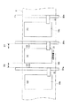
まず、本発明の実施形態に係る液晶表示装置の構成について説明する。図1は、本発明の液晶表示装置100の概略構成を模式的に示す平面図である。図1では、主として、液晶表示装置100の電極及び配線の構成を平面図として示している。ここに、本発明の液晶表示装置100は、TFD素子を用いたアクティブ・マトリクス駆動方式であって、半透過反射型の液晶表示装置である。図2は、図1の液晶表示装置100における切断線A−A’に沿った概略断面図を示す。
[First embodiment]
First, the configuration of the liquid crystal display device according to the embodiment of the present invention will be described. FIG. 1 is a plan view schematically showing a schematic configuration of a liquid
まず、図2を参照して、切断線A−A’に沿った液晶表示装置100の断面構成について説明し、その後、液晶表示装置100の電極及び配線の構成について説明する。
First, the cross-sectional configuration of the liquid
図2において、液晶表示装置100は、素子基板92と、その素子基板92に対向して配置されるカラーフィルタ基板91とが枠状のシール部材3を介して貼り合わされ、内部に液晶が封入されて液晶層4が形成されてなる。この枠状のシール部材3には、複数の金粒子などの導通部材7が混入されている。素子基板92はガラスなどの透明基板1(以下、「上側基板」とも呼ぶ。)を備え、カラーフィルタ基板91は同じくガラスなどの透明基板2(以下、「下側基板」とも呼ぶ。)を備える。
In FIG. 2, the liquid
下側基板2の内面上には、表面上に細かい凹凸が形成された散乱層9が形成されている。散乱層6の内面上は、サブ画素SG毎に、所定の厚みを有する反射層5が形成されている。各反射層5には、矩形状の開口部20(以下、「透明領域」とも呼ぶ。)が複数形成されている。各反射層5は、アルミニウム、アルミニウム合金、銀合金等の薄膜により形成することができる。開口部20は、カラーフィルタ基板91の内面上に縦横にマトリクス状に配列されたサブ画素SG毎に、当該サブ画素SGの全面積を基準として所定割合の面積を有するように形成されている。
On the inner surface of the
反射層5上であって且つ各サブ画素SGの間には、隣接するサブ画素SG間を隔て、一方のサブ画素から他方のサブ画素への光の混入を防止するため、黒色遮光層BMが形成されている。この黒色遮光層BMは、黒色の樹脂材料、例えば黒色の顔料を樹脂中に分散させたもの等を用いることが可能である。なお、これに代えて、R、G、Bの着色層が相互に重ね合わされて形成された重ね遮光層(図示略)を用いてもよい。
On the
また、反射層5上及び開口部20上には、サブ画素SG毎にR、G、Bの三色のいずれかからなる着色層6R、6G、及び6Bが形成されている。着色層6R、6G及び6Bによりカラーフィルタが構成される。画素Gは、R、G、Bのサブ画素SGから構成されるカラー1画素分の領域を示している。なお、以下の説明において、色を問わずに着色層を指す場合は単に「着色層6」と記し、色を区別して着色層を指す場合は「着色層6R」などと記す。また、図2に示すように、開口部20上に形成された着色層6の厚さは、反射層5上に形成された着色層6の厚さよりも厚く形成されている。これにより、着色層6は、反射型表示モードと透過型表示モードとにおいて夫々所望の色相及び明るさを呈するように設計されている。
On the
着色層6及び黒色遮光層BMの上には、透明樹脂等からなる保護層18が形成されている。この保護層18は、カラーフィルタ基板91及び液晶表示装置100の製造工程中に使用される薬剤等による腐食や汚染から、着色層6を保護する機能を有する。保護層18の表面上には、ストライプ状のITO(Indium-Tin Oxide)などの透明電極(走査電極)8(以下、「下側基板2の走査線」とも呼ぶ)が形成されている。この透明電極8の一端はシール部材3内に延在しており、そのシール部材3内の導通部材7と電気的に接続されている。
A
一方、上側基板1の内面上には、サブ画素毎に、TFD素子21及び画素電極10が形成されている。TFD素子21及び画素電極10の内面上には、透明樹脂等からなる保護層19が形成されている。上側基板1及び保護層19の内面上の左右周縁部には、走査線31が形成されている。走査線31の一端部はシール部材3内まで延在しており、その走査線31は、シール部材3内の導通部材7と電気的に接続されている。
On the other hand, the
下側基板2の透明電極8の内面上、及び上側基板1の保護層19の内面上には、それぞれ図示しない配向膜が形成されている。それらの配向膜の間には、液晶層4の厚さを均一に保持するために粒子状のスペーサ(図示略)がランダムに配置されている。スペーサの材料としては、シリカや樹脂などを主成分とするものが好ましい。
An alignment film (not shown) is formed on the inner surface of the
下側基板2の外面上には、位相差板(1/4波長板)11及び偏光板12が配置されており、上側基板1の外面上には、位相差板(1/4波長板)13及び偏光板14が配置されている。また、偏光板12の下側には、バックライト15が配置されている。バックライト15は、例えば、LED(Light Emitting Diode)等といった点状光源や、冷陰極蛍光管等といった線状光源などが好適である。
A retardation plate (¼ wavelength plate) 11 and a polarizing plate 12 are arranged on the outer surface of the
下側基板2の透明電極8、即ち下側基板2の走査線と、上側基板1の走査線31とは、シール部材3内に混入された導通部材7を介して上下導通している。
The
さて、本実施形態の液晶表示装置100において反射型表示がなされる場合、液晶表示装置100に入射した外光は、図1に示す経路Rに沿って進行する。つまり、液晶表示装置100に入射した外光は、反射層5によって反射され観察者に至る。この場合、その外光は、着色層6が形成されている領域を通過して、その着色層6の下側にある反射層5により反射され、再度着色層6を通過することによって所定の色相及び明るさを呈する。こうして、所望のカラー表示画像が観察者により視認される。
When the reflective display is performed in the liquid
一方、透過型表示がなされる場合、バックライト15から出射した照明光は、図1に示す経路Tに沿って進行し、透過領域、即ち、開口部20上の着色層6を通過して観察者に至る。この場合、その照明光は、着色層6を透過することにより所定の色相及び明るさを呈する。こうして、所望のカラー表示画像が観察者により視認される。
On the other hand, when transmissive display is performed, the illumination light emitted from the
次に、図1、図3及び図4を参照して、本発明の素子基板92及びカラーフィルタ基板91の電極及び配線の構成について説明する。図3は、素子基板92を背面方向(即ち、図2における下方)から観察したときの素子基板92の電極及び配線などの構成を平面図として示す。図4は、カラーフィルタ基板91を正面方向(即ち、図2における上方)から観察したときのカラーフィルタ基板91の電極の構成を平面図として示す。なお、図3において電極や配線は観察方向の背面側に形成されるものであるが、説明の便宜上、実線で表すこととしている。また、図3及び図4において、電極や配線以外のその他の要素は説明の便宜上図示を省略している。
Next, with reference to FIG. 1, FIG. 3, and FIG. 4, the configuration of the electrodes and wirings of the
図1において、素子基板92の画素電極10と、カラーフィルタ基板91の透明電極8との交差する領域が表示の最小単位であるサブ画素SGを構成する。そして、このサブ画素SGが紙面縦方向及び紙面横方向に複数個、マトリクス状に並べられた領域が表示領域V(2点鎖線により囲まれる領域)である。この表示領域Vに、文字、数字、図形等の画像が表示される。また、図1において、液晶表示装置100の外形と、表示領域Vとによって区画された領域は、画像表示に寄与しない額縁領域38である。
In FIG. 1, a region where the
先ず、図3を参照して、素子基板92の電極及び配線の構成などについて説明する。素子基板92は、TFD素子21、画素電極10、複数の走査線31、複数のデータ線32、YドライバIC33、XドライバIC34、及び複数の外部接続用端子35を備えている。
First, with reference to FIG. 3, the structure of the electrode and wiring of the
素子基板92の張り出し領域36上には、YドライバIC33及びXドライバIC34が例えばACF(Anisotropic Conductive Film:異方性導電膜)を介して、それぞれ実装されている。なお、図3において、素子基板92の張り出し領域36側の辺92aから反対側の辺92cへ向かう方向をX方向とし、辺92dから辺92bへ向かう方向をY方向とする。
On the projecting
張り出し領域36上には、複数の外部接続用端子35が形成されている。YドライバIC33及びXドライバIC34の各入力端子(図示略)は、導電性を有するバンプを介して、その複数の外部用接続端子35にそれぞれ接続されている。外部接続用端子35は、ACFや半田などを介して、図示しない配線基板、例えばフレキシブルプリント基板に接続されている。これにより、例えば携帯電話や情報端末などの電子機器から液晶表示装置100へ信号や電力が供給される。
A plurality of
XドライバIC34の出力端子(図示略)は、導電性を有するバンプを介して、複数のデータ線32に接続されている。一方、各YドライバIC33の出力端子(図示略)は、導電性を有するバンプを介して、複数の走査線31に接続されている。これにより、各YドライバIC33は複数の走査線31に走査信号を、XドライバIC34は複数のデータ線32にデータ信号をそれぞれ出力する。
The output terminal (not shown) of the
複数のデータ線32は、紙面縦方向に延在する直線状の配線であり、張り出し領域36から表示領域VにかけてX方向に形成されている。各データ線32は一定の間隔を隔てて形成されている。また、各データ線32は、適宜の間隔をおいて複数のTFD素子21に接続されており、各TFD素子21は対応する各画素電極10に接続されている。
The plurality of
複数の走査線31は、本線部分31aと、その本線部分31aに対して略直角に折れ曲がる折れ曲がり部分31bとにより構成されている。各本線部分31aは、額縁領域38内を張り出し領域36からX方向に形成されている。また、各本線部分31aは、各データ線32に対して略平行で、且つ、一定の間隔を隔てて形成されている。各折れ曲がり部分31bは、額縁領域38内において、左右に位置するシール部材3内までY方向に延在している。そして、その折れ曲がり部分31bの終端部は、シール部材3内で導通部材7に接続されている。
The plurality of
次に、カラーフィルタ基板91の電極の構成について説明する。カラーフィルタ基板91は、Y方向にストライプ状の透明電極(走査電極)8が形成されている。各透明電極8の左端部或いは右端部は、図1及び図4に示すように、シール部材3内まで延在しており、且つ、シール部材3内の導通部材7に接続されている。
Next, the configuration of the electrodes of the
以上に述べた、カラーフィルタ基板91と素子基板92とをシール部材3を介して貼り合わせた状態が図1に示されている。図示のように、カラーフィルタ基板91の各透明電極8は、素子基板92の各データ線32に対して直交しており、且つ、横列をなす複数の画素電極10と平面的に重なり合っている。このように、透明電極8と画素電極10とが重なり合う領域がサブ画素SGを構成する。
FIG. 1 shows a state where the
また、カラーフィルタ基板91の透明電極8(即ち、カラーフィルタ基板91側の走査線)と、素子基板92の走査線31とは、図示のように左辺側と右辺側との間で交互に重なり合っており、その透明電極8と走査線31とは、シール部材3内の導通部材7を介して上下導通している。つまり、透明電極8たるカラーフィルタ基板91の各走査線と、素子基板92の各走査線31との導通は、図示のように左辺側と右辺側との間で交互に実現されている。これにより、カラーフィルタ基板91の透明電極8は、素子基板92の走査線31を介して、紙面左右に夫々位置する各YドライバIC33に電気的に接続されている。
Further, the transparent electrode 8 (that is, the scanning line on the
次に、図5を参照して、液晶表示装置100における階調表示の方法について説明する。なお、本例ではノーマリーホワイトの液晶パネルであるとする。図5(a)は、YドライバIC33から走査線31を介して走査電極8に印加される走査電位VAの駆動波形を示す。図5(b)は、XドライバIC34からデータ線32に印加される信号電位VBの駆動波形を示す。図5(c)は、走査電極8及びデータ線32の電極間電圧VABの駆動波形を示す。
Next, a gradation display method in the liquid
YドライバIC33は、走査線31を介して走査電極8に対して走査電位VAを印加する。一方、XドライバIC34は、データ線32に対して信号電位VBを印加する。電位VA及びVBについて説明する。まず、走査電極8には、図5(a)に示すような走査電位VAが印加される。ライン選択期間T毎に、各走査線31を介して各走査電極8は順次選択され、ある共通電位VGNDに対して±Vselなる電位差、即ち電圧を持ついずれかの電位が印加される。なお、この電圧Vselを選択電圧と呼ぶ。そして、ライン選択期間T後には、共通電位VGNDに対して±Vhldなる電圧を持ついずれかの電位が印加される。保持期間Thにおいては、選択時の電位がVGND+VselのときにはVGND+Vhldの電位が印加され、選択時の電位がVGND−VselのときにはVGND−Vhldの電位が印加される。なお、この電圧Vhldを保持電圧と呼ぶ。また、全ての走査電極8が一巡して選択され終わる期間をフィールド期間といい、次のフィールド期間では、先のフィールド期間とは逆特性の選択電圧を用いて順次、走査電極を選択していく。
The
一方、データ線32に対しては、図5(b)に示すように、共通電位VGNDに対して±Vsigなる電圧を持ついずれかの電位が印加される。ここで、ある選択期間に選択された走査電極8に印加する電位がVGND+Vselの場合に、VGND−Vsigをオン電位Von、VGND+Vsigをオフ電位Voffとして用いる。また、ある選択期間に選択された走査電極8に印加する電位がVGND−Vselの場合に、VGND+Vsigをオン電位Von、VGND−Vsigをオフ電位Voffとして用いる。
On the other hand, as shown in FIG. 5B, any potential having a voltage of ± Vsig with respect to the common potential VGND is applied to the
即ち、信号電位VBの各ライン選択期間T内の波形は、当該データ線32に係る列における各画素の階調に応じて設定されるが、まず、信号電位VBは、各ライン選択期間T毎にオン区間とオフ区間に分割され、オン区間においてはオン電位Vonに、オフ区間においてはオフ電位Voffに設定される。即ち、信号電位VBは、階調値に応じてパルス幅変調される。そして、画素に与えるべき階調が高くなるほど(ノーマリーホワイトモードでは暗くなるほど)、オン区間の占める割合が大きく設定される。
That is, the waveform of the signal potential VB in each line selection period T is set according to the gradation of each pixel in the column related to the
次に、走査電極8及びデータ線32の電極間電圧VABを図5(c)の実線で示す。この電極間電位VABが液晶層4に対して印加される。図示のように、電極間電圧VABの絶対値は、当該画素の選択期間において高くなることがわかる。また、液晶層4に印加される液晶層電圧VLCは、図5(c)のハッチングで示すようになる。液層層電圧VLCが変化する際には、液晶層4が形成する容量を充放電しなければならないため、液晶層電圧VLCは電極間電圧VABに対して過渡応答的に変化する。なお、図5(c)において電圧VNLは電極間電圧VABと液層層電圧VLCとの差、即ちTFD素子21の端子電圧である。以上のように、液晶表示装置100では、液晶層4に印加する駆動電圧をパルス幅変調することにより階調表示が行われる。
Next, the interelectrode voltage VAB of the
[縦クロストークの発生原理]
まず、図6を参照して、縦クロストークについて説明する。図6は、液晶表示装置100における表示領域Vのみを拡大した平面図であり、その表示領域Vに縦クロストークが発生した状態を模式的に示している。
[Generation principle of vertical crosstalk]
First, vertical crosstalk will be described with reference to FIG. FIG. 6 is a plan view in which only the display area V in the liquid
液晶表示装置100に対しては、背景となるエリアB及びエリアCをそれぞれ同一のグレーレベルとなるように走査線電圧及びデータ線電圧を印加している。また、エリアAにおいては、規定の明るさの単色或いは補色の矩形表示となるように走査線電圧及びデータ線電圧を印加している。しかし、実際には縦クロストークの発生により同一階調レベルであるはずのエリアBとエリアCでは表示画像上のグレーレベルが異なってしまっている。即ち、エリアAの上下方向に位置するエリアCは、エリアBよりも幾分明るく表示されており、尚且つ微妙に色づいて表示されている。また、エリアAは、規定の明るさよりも暗く表示されている。このような、縦クロストークは、灰色などを背景にして単色或いは補色の矩形表示をしたときに発生する。
A scanning line voltage and a data line voltage are applied to the liquid
次に、図7を参照して、この縦クロストークの発生原理について説明する。図7は、液晶表示装置100における1画素(RGB3つのサブ画素)分を拡大した部分拡大平面図を示す。
Next, the principle of occurrence of this vertical crosstalk will be described with reference to FIG. FIG. 7 shows a partially enlarged plan view in which one pixel (RGB three subpixels) in the liquid
画素電極10は、通常、一対のデータ線32の略中央位置に形成される。これは、画素電極10を隣接する各データ線32に近づけすぎない範囲で、その画素の開口率を大きくするという設計上の理由によるものである。また、各データ線32a、32b、32cは、TFD素子21を介して画素電極10a、10b、10cに接続されている。例えば、画素電極10bに注目すると、データ線32aは、画素電極10bに隣接しているが、画素電極10bには接続されていない。画素電極10bと、隣接する2つのデータ線32a及び32bとの間には寄生容量C2、C1がそれぞれ存在する。
The
液晶表示装置100において、所望する画像を表示するためには、ライン選択期間Tに、各画素電極10a〜10cに所望の電圧が印加される。図7の例では、画素電極10bに対しては、データ線32bからTFD素子21を介して所望の電圧Vlcが印加される。
In the liquid
ところが、画素電極10bに対しては、それと隣接するデータ線32aとの間の寄生容量C2が存在することにより、データ線32aから寄生容量C2に対応する電圧が印加されてしまい、その結果、画素電極10bの電位Vlcが所望の電位から変化してしまう。即ち、ある画素電極の電位が、それと隣接するデータ線との間の寄生容量に起因して変化してしまう。これにより、当該画素の透過率が変化し、縦クロストークが生じる。
However, since the parasitic capacitance C2 between the
いま、図6においてエリアAに青を表示し、エリアB及びCにグレーを表示したとする。図7において、データ線32aに対応する画素電極10aが青に対応するサブ画素であり、画素電極10bが赤に対応するサブ画素であり、最も右の画素電極10cが緑に対応するサブ画素であるとする。
In FIG. 6, it is assumed that blue is displayed in area A and gray is displayed in areas B and C. In FIG. 7, the
これら3色のサブ画素が図6におけるエリアBに存在する場合には、そのエリアがグレー表示されるので、3つのデータ線32a、32b、32に印加される電圧はほぼ等しく、寄生容量C2が画素電極10bに与える影響は少ない。
When these three color sub-pixels are present in area B in FIG. 6, the area is displayed in gray, so that the voltages applied to the three
一方、エリアAに青が表示されているので、エリアCにおいてもデータ線32aのみが低電位(白に対応する電位)であり、データ線32b及び32cは高電位(黒に対応する電位)になる。よって、エリアCでは、保持期間においてデータ線32aと画素電極10bとに電位差が生じ、寄生容量C2により画素電極10bの電位が下がる。その結果、画素電極10bにより構成される赤のサブ画素の透過率が上がり、エリアCの部分は明るくなるとともに、いくぶん赤みを帯びて見えるようになる。これが、縦クロストークの発生する原理である。つまり、縦クロストークは、寄生容量C2の影響によって、隣接する画素電極の電位が所望の電位から変化することにより生じる。
On the other hand, since blue is displayed in the area A, only the
[縦クロストークの低減方法]
次に、図8及び図9を参照して、縦クロストークの低減方法について述べる。図8及び図9は、図7の一部に対応し、本発明の第1実施形態に係る縦クロストークを低減する方法を説明する図である。なお、以下では、説明の便宜上、図8及び図9に示される、1つの画素電極10bと、その両側に位置するデータ線32a、32bとに着目して説明する。
[How to reduce vertical crosstalk]
Next, a method for reducing vertical crosstalk will be described with reference to FIGS. 8 and 9 correspond to a part of FIG. 7 and are diagrams for explaining a method of reducing vertical crosstalk according to the first embodiment of the present invention. In the following description, for the convenience of description, the description will be given focusing on one
上記のように、縦クロストークは、隣接するデータ線との間の寄生容量C2の影響により、画素電極の電圧Vlcが変化するために生じる。したがって、縦クロストークを低減するには、寄生容量C2を小さくし、寄生容量C2による影響を低減すればよい。 As described above, the vertical crosstalk occurs because the voltage Vlc of the pixel electrode changes due to the influence of the parasitic capacitance C2 between the adjacent data lines. Therefore, in order to reduce the vertical crosstalk, the parasitic capacitance C2 may be reduced to reduce the influence of the parasitic capacitance C2.
一般に、ある物質の静電容量Cは、
C=ε0・ε(S/d) (式1)
で表される。なお、C=静電容量、ε0=真空の誘電率、ε=比誘電率、S=面積、d=間隔である。よって、上記の式1に従えば、寄生容量C2を小さくするためには、dの値、即ち、データ線32aと画素電極10bとの距離D2を大きくすればよい。
In general, the capacitance C of a substance is
C = ε0 · ε (S / d) (Formula 1)
It is represented by Note that C = capacitance, ε0 = dielectric constant in vacuum, ε = dielectric constant, S = area, and d = interval. Therefore, according to the
そこで、本発明では、寄生容量C2を小さくするために、画素電極10bとそれに接続されたデータ線32bとの間隔D1よりも、画素電極10bとそれに接続されていない隣接するデータ線32aとの間隔D2を広くする。つまり、D1<D2の関係が成り立つようにする。これにより、上記の式1において、間隔d、即ち間隔D2が大きくなるので、寄生容量C2を小さくすることができる。なお、本実施形態において、画素電極10bと、それに接続されたデータ線32bとの間隔D1は好ましくは2.5μm程度である。また、画素電極10bはデータ線32b側に近づくため寄生容量C1は大きくなるがこの寄生容量C1は、TFD素子21を介して画素電極10bに接続されたデータ線32b側に生じるので、寄生容量C2と比べて表示画像に与える影響は小さい。
Therefore, in the present invention, in order to reduce the parasitic capacitance C2, the distance between the
以上のようにして、寄生容量C2を小さくすることにより縦クロストークを効果的に低減することができる。よって、液晶表示装置100において、灰色などを背景色に、単色或いは補色などの矩形表示をした場合でも高品位な表示画像が得られる。
As described above, the vertical crosstalk can be effectively reduced by reducing the parasitic capacitance C2. Therefore, in the liquid
なお、画素電極10bとそれに接続されたデータ線32bとの間隔D1を狭くするのには、設計上の理由などによりある程度限界がある。この場合には、図9に示すように、画素の開口率は若干下がるが、画素電極10bを、データ線32aに対向する側の領域の一部、即ち、領域E2に相当する部分だけ小さく形成することとしてもよい。これにより、間隔D1をある程度保ちつつ、画素電極10bとそれに接続されていないデータ線32aとの間隔D2を大きくすることができる。
Note that there is a certain limit to reducing the distance D1 between the
[第2実施形態]
上記の第1実施形態に係る液晶表示装置100では、素子基板92の上側基板1上にデータ線32及び画素電極10等を夫々形成して、画素電極10とそれに接続されていないデータ線32との間隔を大きくして寄生容量を小さくし、縦クロストークを低減するようにした。第2実施形態では、素子基板92の構成を変え、画素電極10とデータ線32とを絶縁層で絶縁する。これに加え、第1実施形態と同様に、画素電極10と、それが接続されていない隣接するデータ線との間隔D2を、接続されているデータ線との間隔D1より大きくする。これにより、画素電極10とそれに接続されていないデータ線32aとの寄生容量を減少させ縦クロストークを低減する。
[Second Embodiment]
In the liquid
以下、図10を参照して、第2実施形態による縦クロストークを低減する方法について説明する。図10(a)は、第2実施形態の素子基板92’の局部平面図を示す。図10(b)は、図10(a)における切断線B−B’に沿った断面図を示す。なお、以下では、説明の便宜上、図10(a)に示される、1つの画素電極10bと、その両側のデータ線32a及び32bとに着目して説明する。
Hereinafter, a method of reducing vertical crosstalk according to the second embodiment will be described with reference to FIG. FIG. 10A shows a local plan view of the
まず、素子基板92’の構成について述べる。素子基板92’を構成する上側基板1の内面上には、複数のデータ線32が形成されている。一方、上側基板1の外面上には、位相差板(1/4波長板)13及び偏光板14が配置されている。
First, the configuration of the element substrate 92 'will be described. A plurality of
また、図10(a)に示すように、各データ線32は、XドライバIC34に接続された帯状の本線32fと、その本線32fから引き出された引き出し線32gとを有する。引き出し線32gは、サブ画素毎に、画素電極10b側に延び出るように形成されている。この引き出し線32gの一部及びそれに近接する上側基板1の各内面上には、Ta2O5などからなる絶縁層50が積層されている。そして、その絶縁層50及びそれに近接する上側基板1の各内面上には、TFD素子21が形成されている。また、上側基板1の内面上には、絶縁層17が積層されている。これにより、TFD素子21及びデータ線32は絶縁層17により覆われている。なお、このようにデータ線32及びTFD素子21と画素電極10bとの間に絶縁層17を設ける構造はオーバーレイヤー構造とも呼ばれ、絶縁層17はオーバーレイヤー層とも呼ばれる。なお、絶縁層17の表面は平坦であり、絶縁層17の膜厚は好ましくは1〜3μm、最適には2μmである。
As shown in FIG. 10A, each
絶縁層17は、画素電極10bの一部とTFD素子21とが対向する位置にコンタクトホール17a、即ち開口を有する。画素電極10bの一部は、コンタクトホール17aを通じてTFD素子21と接続されている。このため、画素電極10bは、TFD素子21を介して、データ線32に接続されている。
The insulating
図10(a)において、画素電極10bとそれが接続されていないデータ線32aとの間隔D2は、それが接続されているデータ線32bとの間隔D1より大きくする。これは、第1実施形態と同様である。よって、画素電極10bとそれに接続されていないデータ線32aとの間の寄生容量を低減することができる。これにより、縦クロストークを効果的に低減することができ、第1実施形態の液晶表示装置と同様に高品位な表示画像が得られる。
In FIG. 10A, the interval D2 between the
図10(a)における切断線C−C’に沿った断面図を図10(c)に示す。本実施形態では、図10(c)に示すようにデータ線32上に樹脂などにより絶縁層17が形成され、その上に画素電極10bが形成されている。従って、第1実施形態のようにデータ線32と画素電極10とが同一面上に形成される場合と比較して、画素電極10bと、それが接続されていない方の隣接するデータ線32aとの距離D3は、絶縁層17の厚さ分だけさらに大きくなる。即ち、図10(c)に示すように、右側の画素電極10bは図10(a)に示す平面上で隣接するデータ線32aと間隔D2だけ離れて形成されるが、実際には図10(c)に示すように絶縁層17の厚さがあるので、画素電極10bとデータ線32aとの距離はD3(>D2)となる。よって、隣接するデータ線との間の寄生容量をより小さくすることができる。即ち、第2実施形態では、絶縁層17の厚さ分だけ、画素電極を当該画素電極が接続されていない方の隣接するデータ線からさらに遠ざけることができ、それによりそのデータ線からの寄生容量をさらに低減できる利点がある。
FIG. 10C shows a cross-sectional view along the cutting line C-C ′ in FIG. In the present embodiment, as shown in FIG. 10C, the insulating
また、第1実施形態では、データ線32と画素電極10とは同一面上に形成され、両者の間には液晶が介在する。これに対し、第2実施形態では図10(c)に示すように、データ線32aと画素電極10bとの間には絶縁層17が介在する。一般的に絶縁層17を形成する樹脂の誘電率は液晶の誘電率より小さい。よって、上記の式1から理解されるように、データ線32aと画素電極10bとの間に誘電率の小さい絶縁層17が存在する方が、より寄生容量を低減することができるという利点がある。
また、第2実施形態では、画素電極10bとデータ線32aとは絶縁層17により絶縁されている。よって、間隔D2を大きくするために画素電極10bを図10(a)における右方向、即ちデータ線32bの方向にデータ線32bのかなり近傍まで移動させたとしても、画素電極10bとデータ線32bとが導通してしまうことはない。即ち、第1実施形態と比較すると、データ線32bとの導通という問題がないので、画素電極10bとデータ線32aとの間隔D2を増大させる自由度が大きくなるという利点を有する。
In the first embodiment, the
In the second embodiment, the
この点について、図11を参照して説明する。図11(a)は、絶縁層17を有するオーバーレイヤー構造の液晶表示装置において、基板に垂直な方向から平面視した場合に、画素電極10bの端部をそれが接続されているデータ線32bの端部と一致する位置に形成した例を示す。即ち、図11(a)に示すように、右側の画素電極10bの信号線32bとの間隔D1はほぼ零(0)である。
This point will be described with reference to FIG. FIG. 11A shows an overlayer-structured liquid crystal display device having an insulating
また、図11(b)は図11(a)の切断線C−C’における断面図であり、画素電極10bの信号線32b側の端部と、信号線32bの画素電極10b側の端部はラインF上において一致している。このように、第2実施形態では、画素電極10bとデータ線32bとの間に絶縁層17が形成されており導通の恐れがないので、両者を十分に接近させることができる。これにより、画素電極10bと、それが接続されていない方の隣接するデータ線32aとの間隔を十分に確保することができ、その間の寄生容量を十分に低減することが可能となる。なお、画素電極10bをデータ線32bの上方に配置し、画素電極10bとデータ線32bを重ねてしまっても絶縁層17が介在しているので導通の恐れはないが、データ線32bを重ねた領域分だけ表示領域が狭くなり開口率が下がる。よって、開口率の低下を招かないためには、両者を重ねずにできる限り両者を近接させることが望ましい。本実施形態において、画素電極10bと、それに接続されたデータ線32bとの平面的に見た間隔D1は好ましくは0〜2.5μmである。
FIG. 11B is a cross-sectional view taken along the section line CC ′ of FIG. 11A, and the end of the
[第3実施形態]
第3実施形態は、本発明をいわゆる垂直配向方式の液晶表示装置に適用したものである。液晶分子の配向を制御することにより視野角依存性を改善し、広視野角化を図った垂直配向方式の液晶装置が知られている。垂直配向方式の液晶装置では、負の誘電率異方性を有する液晶を使用し、素子基板と対向基板との間に電圧が印加されていない状態では、液晶分子は基板に対して略垂直の方向に配向する。スイッチング素子としてTFTやTFDが設けられた素子基板には、略円形又は多角形の複数のサブ画素電極を含んでなる画素電極が形成される。また、対向基板には、各サブ画素電極の略中央に対向する位置にスリット又は凸部(突起)などが形成される。素子基板と対向基板との間に電圧を印加すると、基板間の液晶層には電圧に応じた電界が形成されるが、サブ画素電極が略円形又は多角形などに形成されており、かつ、それと対向する対向基板側の電極にはスリットや凸部などが形成されているため、液晶分子はサブ画素電極の略中央を中心として放射状に配向状態が制御される。これにより、視野角依存性が抑制され、広視野角化が可能となる。
[Third Embodiment]
In the third embodiment, the present invention is applied to a so-called vertical alignment type liquid crystal display device. 2. Description of the Related Art A vertical alignment type liquid crystal device is known in which viewing angle dependency is improved by controlling the alignment of liquid crystal molecules and a wide viewing angle is achieved. In a vertical alignment type liquid crystal device, a liquid crystal having a negative dielectric anisotropy is used, and in a state where no voltage is applied between the element substrate and the counter substrate, the liquid crystal molecules are substantially perpendicular to the substrate. Oriented in the direction. A pixel electrode including a plurality of substantially circular or polygonal sub-pixel electrodes is formed on an element substrate provided with TFTs and TFDs as switching elements. In addition, a slit or a convex portion (protrusion) is formed on the counter substrate at a position facing substantially the center of each subpixel electrode. When a voltage is applied between the element substrate and the counter substrate, an electric field corresponding to the voltage is formed in the liquid crystal layer between the substrates, but the subpixel electrode is formed in a substantially circular or polygonal shape, and Since a slit, a convex part, or the like is formed on the electrode on the counter substrate facing the liquid crystal molecule, the alignment state of the liquid crystal molecules is controlled radially about the center of the sub-pixel electrode. Thereby, the viewing angle dependency is suppressed, and a wide viewing angle can be achieved.
図12(a)は垂直配向方式を採用した第3実施形態による液晶表示装置の素子基板92vの一部を示す。図12(b)は、図12(a)の切断面C−C’における素子基板92vの断面図であり、図13(a)は同じく図12(a)の切断面C−C’における素子基板92v及びそれに対向するカラーフィルタ基板91の断面図である。
FIG. 12A shows a part of the
第2実施形態と比較して説明すると、第3実施形態の素子基板92vでは、画素電極10vは複数の円形又は多角形の画素電極を接続して構成される。1つの画素電極10vを複数の多角形の電極により構成する理由は、個々の円形又は多角形の電極がある程度小さいほうが、液晶分子の配向状態を制御し易いからである。なお、説明の便宜上、図12(a)及び(b)において、画素電極10vのうち左側の列の画素電極を10vaとし、右側の列の画素電極を10vbとする。また、以下の説明は主に画素電極10vbに着目して行う。
In comparison with the second embodiment, in the
図12(a)に示すように、各データ線32は、XドライバIC34に接続された帯状の本線32fと、その本線32fから引き出された引き出し線32gとを有する。引き出し線32gは、画素電極10v側に延び出るように形成されている。この引き出し線32gの一部及びそれに近接する上側基板1の各内面上には、Ta2O5などからなる絶縁層が積層されている。そして、その絶縁層及びそれに近接する上側基板1の各内面上には、TFD素子21が形成されている。また、上側基板1の内面上には、絶縁層17が積層されている。これにより、TFD素子21及びデータ線32は絶縁層17により覆われている。即ち、第3実施形態の液晶表示装置もいわゆるオーバーレイヤー構造を採用している。
As shown in FIG. 12A, each
絶縁層17は、画素電極10vの一部とTFD素子21とが対向する位置にコンタクトホール(図示略)を有し、画素電極10vの一部(図12(a)における下端部)は、コンタクトホールを通じてTFD素子21と接続されている。このため、画素電極10vは、TFD素子21を介して、データ線32に接続されている。
The insulating
第1及び第2実施形態と同様に、図12(a)において、画素電極10vbとそれが接続されていないデータ線32aとの間隔D2は、それが接続されているデータ線32bとの間隔D1より大きい。よって、画素電極10vbとそれに接続されていないデータ線32aとの間の寄生容量を低減することができる。これにより、縦クロストークを効果的に低減することができ、高品位な表示画像が得られる。また、第3実施形態においても、第2実施形態と同様に、データ線32aと画素電極10vとの間に絶縁層17が存在するので、両者の距離を絶縁層17の厚さ分だけさらに遠ざけることができること、及び、絶縁層17の誘電率が液晶の誘電率よりも小さいことにより、さらにデータ線32aと画素電極10vbとの間の寄生容量を低減することが可能となる。
Similar to the first and second embodiments, in FIG. 12A, the distance D2 between the pixel electrode 10vb and the
次に、図13を参照して、1つの画素電極10v付近の断面構成について説明する。なお、図13では、対向するカラーフィルタ基板91側の構成も示されている。
Next, a cross-sectional configuration near one
図13(a)は、図12(a)におけるC−C’に沿った模式断面図である。図示のように、素子基板92vの基板1の内面上にはデータ線32が形成される。また、基板1の内面上及びデータ線32上にはオーバーレイヤー層としての絶縁層17が形成され、その絶縁層17上に画素電極10vが形成される。なお、絶縁層17上及び画素電極10v上には垂直配向膜が形成される(図示略)。
FIG. 13A is a schematic cross-sectional view taken along C-C ′ in FIG. As shown,
一方、対向側の基板2の内面上には樹脂散乱膜9が形成され、その樹脂散乱膜9上には反射膜5が形成される。また、反射膜5の内面上には、カラーフィルタ6及び黒色遮光膜BMが形成される。また、カラーフィルタ6及び黒色遮光膜BMの内面上には平坦化膜18が形成され、その平坦化膜18上には走査線8が形成される。
On the other hand, a
ここで、走査線8には、各画素電極10vを構成する複数の多角形電極の略中心に対応する位置に開口8sが形成されている。基板間に電圧が印加されると、開口8sと画素電極10vの相互作用により、その部分に斜め電界が生じ(図中の矢印を参照)、液晶分子4vの傾倒方向が規定される。このため、基板間に印加する電圧の大きさに応じて液晶分子4vの配向状態を放射状に制御することができる。よって、液晶分子4vが放射状に配向した領域が形成される。
Here, an
図13(b)に対向基板2側の他の構造例を示す。この例では、走査線8上には、各画素電極10の多角形電極の略中心に対応する位置に樹脂などからなる突起、即ち凸部Tが形成されている。これにより、液晶の初期配向状態において、液晶分子4vは、その凸部Tの傾斜面に沿って配向される。これにより、液晶分子4vの傾倒方向が規定される。
FIG. 13B shows another structural example on the
また、本実施形態では、第2実施形態と同様にオーバーレイヤー構造を採用しているので、第2実施形態において図11を参照して説明したのと同様に、画素電極10vとそれが接続される側のデータ線32bとを限りなく近づけることができる。この例を図14(a)及び(b)に示す。図14(a)は素子基板の平面図であり、図14(b)はその切断面C−C’における断面図である。なお、本実施形態は、第2実施形態と同様に、画素電極10vとデータ線32bを重ねると開口率が下がるので、両者を重ならない範囲で近接させるのが望ましい。本実施形態において、画素電極10vbと、それに接続されたデータ線32bとの平面的に見た間隔D1は好ましくは0〜2.5μmである。
In the present embodiment, since an overlayer structure is adopted as in the second embodiment, the
以上のように、第3実施形態によれば、オーバーレイヤー構造を備える垂直配向方式の液晶表示装置においても、本発明を適用することができる。 As described above, according to the third embodiment, the present invention can also be applied to a vertical alignment type liquid crystal display device having an overlayer structure.
(変形例)
上記の実施形態では、半透過反射型の液晶表示装置100に本発明を適用したが、これに限らず、反射型又は透過型の液晶表示装置にも本発明を適用できる。また、上記実施形態では、ノーマリーホワイト型の液晶表示装置100に本発明を適用したが、これに限らず、ノーマリーブラック型の液晶表示装置にも本発明を適用できる。
(Modification)
In the above embodiment, the present invention is applied to the transflective liquid
また、上記の各実施形態では、スイッチング素子として薄膜トランジスタ(TFD)素子を用いた例について説明したが、本発明の適用はこれには限定されない。スイッチング素子の他の例としてアモルファスTFTの断面図を図15に示す。図15において、TFT450は、図示しないゲート線から分岐したゲート電極402の上に、それを覆うようにゲート絶縁膜403が設けられている。ゲート絶縁膜403の上には、ゲート電極402に重なるようにa−Si層405が設けられている。a−Si層405の上には、2つに分断されたn+−a−Si層406a、406bが設けられている。さらに、n+−a−Si層406aの上には図示しないソース線から分岐したソース電極408が設けられ、n+−a−Si層406bの上にはドレイン電極409が設けられている。ドレイン電極409の上には、画素電極410が部分的に重なるように設けられている。そして、それらの層を覆うように保護膜411が設けられている。
Further, in each of the above embodiments, an example in which a thin film transistor (TFD) element is used as a switching element has been described, but application of the present invention is not limited to this. FIG. 15 shows a cross-sectional view of an amorphous TFT as another example of the switching element. In FIG. 15, a
本発明は、スイッチング素子として、上記のようなアモルファスTFTのドレイン電極409と画素電極410との接続部分にも適用することができる。
The present invention can also be applied to a connection portion between the
[電子機器]
次に、本発明による液晶表示装置100を電子機器の表示装置として用いる場合の実施形態について説明する。
[Electronics]
Next, an embodiment in which the liquid
図16は、第1及び第2実施形態の全体構成を示す概略構成図である。ここに示す電子機器は、上記の液晶表示装置100と、これを制御する制御手段410とを有する。ここでは、液晶表示装置100を、パネル構造体403と、半導体ICなどで構成される駆動回路402とに概念的に分けて描いてある。また、制御手段410は、表示情報出力源411と、表示情報処理回路412と、電源回路413と、タイミングジェネレータ414と、を有する。
FIG. 16 is a schematic configuration diagram showing the overall configuration of the first and second embodiments. The electronic apparatus shown here includes the liquid
表示情報出力源411は、ROM(Read Only Memory)やRAM(Random Access Memory)などからなるメモリと、磁気記録ディスクや光記録ディスクなどからなるストレージユニットと、デジタル画像信号を同調出力する同調回路とを備え、タイミングジェネレータ414によって生成された各種のクロック信号に基づいて、所定フォーマットの画像信号などの形で表示情報を表示情報処理回路412に供給するように構成されている。
The display
表示情報処理回路412は、シリアル−パラレル変換回路、増幅・反転回路、ローテーション回路、ガンマ補正回路、クランプ回路などの周知の各種回路を備え、入力した表示情報の処理を実行して、その画像情報をクロック信号CLKとともに駆動回路402へ供給する。駆動回路402は、走査線駆動回路、データ線駆動回路及び検査回路を含む。また、電源回路413は、上述の各構成要素にそれぞれ所定の電圧を供給する。
The display
次に、本発明に係る液晶表示装置100を適用可能な電子機器の具体例について図17を参照して説明する。
Next, specific examples of electronic devices to which the liquid
まず、本発明に係る液晶表示装置100を、可搬型のパーソナルコンピュータ(いわゆるノート型パソコン)の表示部に適用した例について説明する。図17(a)は、このパーソナルコンピュータの構成を示す斜視図である。同図に示すように、パーソナルコンピュータ710は、キーボード711を備えた本体部712と、本発明に係る液晶表示パネルを適用した表示部713とを備えている。
First, an example in which the liquid
続いて、本発明に係る液晶表示装置100を、携帯電話機の表示部に適用した例について説明する。図17(b)は、この携帯電話機の構成を示す斜視図である。同図に示すように、携帯電話機720は、複数の操作ボタン721のほか、受話口722、送話口723とともに、本発明に係る液晶表示装置100を適用した表示部724を備える。
Next, an example in which the liquid
なお、本発明に係る液晶表示装置100を適用可能な電子機器としては、図17(a)に示したパーソナルコンピュータや図17(b)に示した携帯電話機の他にも、液晶テレビ、ビューファインダ型・モニタ直視型のビデオテープレコーダ、カーナビゲーション装置、ページャ、電子手帳、電卓、ワードプロセッサ、ワークステーション、テレビ電話、POS端末、ディジタルスチルカメラなどが挙げられる。
Electronic devices to which the liquid
1 上側基板、 2 下側基板、 3 シール部材、 6 着色層、 7 導通部材、 8 走査電極、 10、10a〜10c 画素電極、 31 走査線、 32、32a、32b データ線、 21 TFD素子、 91 カラーフィルタ基板、 92、92’ 素子基板、 100 液晶表示装置
DESCRIPTION OF
Claims (4)
前記信号線の各々と複数のスイッチング素子を介して接続された複数の画素電極とを有する基板を備え、
前記各画素電極と当該各画素電極に接続されていない隣接する信号線との間隔は、前記各画素電極と当該各画素電極に前記各スイッチング素子を介して接続された信号線との間隔より広く、
前記基板を平面的に見た場合において、前記各画素電極と、当該画素電極に前記各スイッチング素子を介して接続された信号線との間隔は零であり、
さらに前記基板は、前記複数の信号線及び前記複数のスイッチング素子を覆う絶縁層を備え、
前記画素電極の各々は前記絶縁層上に形成されており、当該画素電極の各々の一部は、前記絶縁層に形成された各開口を通じて、対応する前記スイッチング素子の各々に接続されていることを特徴とする液晶表示装置。 Multiple signal lines,
A substrate having each of the signal lines and a plurality of pixel electrodes connected via a plurality of switching elements;
An interval between each pixel electrode and an adjacent signal line not connected to the pixel electrode is wider than an interval between the pixel electrode and a signal line connected to the pixel electrode via the switching element. ,
When the substrate is viewed in plan, the interval between each pixel electrode and the signal line connected to the pixel electrode via each switching element is zero.
Further, the substrate includes an insulating layer that covers the plurality of signal lines and the plurality of switching elements,
Each of the pixel electrodes is formed on the insulating layer, and a part of each of the pixel electrodes is connected to each of the corresponding switching elements through each opening formed in the insulating layer. A liquid crystal display device.
前記対向電極は、前記画素電極に対向する領域に開口又は突起を有し、
前記基板と前記対向基板との間には負の誘電率異方性を有する液晶層が挟持されていることを特徴とする請求項1または2に記載の液晶表示装置。 A counter substrate disposed opposite to the substrate and having a counter electrode on the substrate side;
The counter electrode has an opening or a protrusion in a region facing the pixel electrode,
The liquid crystal display device according to claim 1 , wherein a liquid crystal layer having negative dielectric anisotropy is sandwiched between the substrate and the counter substrate.
Priority Applications (1)
| Application Number | Priority Date | Filing Date | Title |
|---|---|---|---|
| JP2004138610A JP4453434B2 (en) | 2004-03-30 | 2004-05-07 | Liquid crystal device and electronic device |
Applications Claiming Priority (2)
| Application Number | Priority Date | Filing Date | Title |
|---|---|---|---|
| JP2004099209 | 2004-03-30 | ||
| JP2004138610A JP4453434B2 (en) | 2004-03-30 | 2004-05-07 | Liquid crystal device and electronic device |
Publications (3)
| Publication Number | Publication Date |
|---|---|
| JP2005316338A JP2005316338A (en) | 2005-11-10 |
| JP2005316338A5 JP2005316338A5 (en) | 2006-10-19 |
| JP4453434B2 true JP4453434B2 (en) | 2010-04-21 |
Family
ID=35443811
Family Applications (1)
| Application Number | Title | Priority Date | Filing Date |
|---|---|---|---|
| JP2004138610A Active JP4453434B2 (en) | 2004-03-30 | 2004-05-07 | Liquid crystal device and electronic device |
Country Status (1)
| Country | Link |
|---|---|
| JP (1) | JP4453434B2 (en) |
Cited By (1)
| Publication number | Priority date | Publication date | Assignee | Title |
|---|---|---|---|---|
| WO2021227149A1 (en) * | 2020-05-14 | 2021-11-18 | 深圳市华星光电半导体显示技术有限公司 | Array substrate and manufacturing method thereof |
Families Citing this family (8)
| Publication number | Priority date | Publication date | Assignee | Title |
|---|---|---|---|---|
| WO2014061659A1 (en) * | 2012-10-19 | 2014-04-24 | シャープ株式会社 | Liquid crystal display device |
| KR20150033404A (en) * | 2013-09-24 | 2015-04-01 | 하이디스 테크놀로지 주식회사 | Liquid crystal display device |
| KR102010493B1 (en) * | 2015-08-25 | 2019-08-14 | 하이디스 테크놀로지 주식회사 | Liquid crystal display device |
| CN106802522B (en) * | 2017-03-10 | 2019-08-13 | 深圳市华星光电技术有限公司 | Thin-film transistor array base-plate and display panel |
| JP6862258B2 (en) * | 2017-04-20 | 2021-04-21 | 株式会社ジャパンディスプレイ | Display device |
| CN108020970A (en) * | 2017-11-30 | 2018-05-11 | 深圳市华星光电技术有限公司 | Array base palte and liquid crystal display panel |
| CN111090203B (en) | 2020-03-22 | 2020-07-14 | 深圳市华星光电半导体显示技术有限公司 | Array substrate and display panel |
| CN111090204A (en) * | 2020-03-22 | 2020-05-01 | 深圳市华星光电半导体显示技术有限公司 | Array substrate and display panel |
-
2004
- 2004-05-07 JP JP2004138610A patent/JP4453434B2/en active Active
Cited By (1)
| Publication number | Priority date | Publication date | Assignee | Title |
|---|---|---|---|---|
| WO2021227149A1 (en) * | 2020-05-14 | 2021-11-18 | 深圳市华星光电半导体显示技术有限公司 | Array substrate and manufacturing method thereof |
Also Published As
| Publication number | Publication date |
|---|---|
| JP2005316338A (en) | 2005-11-10 |
Similar Documents
| Publication | Publication Date | Title |
|---|---|---|
| US7859630B2 (en) | Electric field driving device, liquid crystal device and electronic apparatus | |
| JP4572854B2 (en) | Liquid crystal device and electronic device | |
| JP3772842B2 (en) | Liquid crystal device, driving method thereof, and electronic apparatus | |
| US7688408B2 (en) | Liquid crystal device and electronic apparatus | |
| USRE45188E1 (en) | Electric field driving device and electronic apparatus | |
| US20150077690A1 (en) | Liquid crystal device and electronic apparatus | |
| JP2007226175A (en) | Liquid crystal device and electronic equipment | |
| US7068338B2 (en) | Electro-optical device substrate, electro-optical device, and electronic apparatus | |
| JP2006126788A (en) | Liquid crystal device and electronic apparatus | |
| JP4952166B2 (en) | Liquid crystal device | |
| JP5522243B2 (en) | Electric field driving apparatus and electronic apparatus | |
| JP2007139948A (en) | Electrooptical device and electronic equipment | |
| JP2007226200A (en) | Liquid crystal device, and electronic device | |
| JP4453434B2 (en) | Liquid crystal device and electronic device | |
| JP2007094025A (en) | Electrooptic device and electronic equipment | |
| JP2006259501A (en) | Liquid crystal device and electronic equipment | |
| JP2006017897A (en) | Electro-optical apparatus and electronic appliance | |
| JP2006091486A (en) | Electro-optical device and electronic equipment | |
| JP2007086506A (en) | Electrooptical device and electronic equipment | |
| JP2004258365A (en) | Electrooptical device and electronic apparatus using it | |
| JP4052293B2 (en) | Liquid crystal device and electronic device | |
| JP2005284056A (en) | Liquid crystal display and electronic equipment | |
| JP2007065602A (en) | Liquid crystal device and electronic apparatus | |
| JP2006091504A (en) | Electrooptical device and electronic equipment | |
| JP4305551B2 (en) | Transflective liquid crystal device and electronic device using the same |
Legal Events
| Date | Code | Title | Description |
|---|---|---|---|
| A521 | Request for written amendment filed |
Free format text: JAPANESE INTERMEDIATE CODE: A523 Effective date: 20060830 |
|
| A621 | Written request for application examination |
Free format text: JAPANESE INTERMEDIATE CODE: A621 Effective date: 20060830 |
|
| A977 | Report on retrieval |
Free format text: JAPANESE INTERMEDIATE CODE: A971007 Effective date: 20090911 |
|
| A131 | Notification of reasons for refusal |
Free format text: JAPANESE INTERMEDIATE CODE: A131 Effective date: 20091027 |
|
| A521 | Request for written amendment filed |
Free format text: JAPANESE INTERMEDIATE CODE: A523 Effective date: 20091209 |
|
| TRDD | Decision of grant or rejection written | ||
| A01 | Written decision to grant a patent or to grant a registration (utility model) |
Free format text: JAPANESE INTERMEDIATE CODE: A01 Effective date: 20100112 |
|
| A01 | Written decision to grant a patent or to grant a registration (utility model) |
Free format text: JAPANESE INTERMEDIATE CODE: A01 |
|
| A61 | First payment of annual fees (during grant procedure) |
Free format text: JAPANESE INTERMEDIATE CODE: A61 Effective date: 20100125 |
|
| FPAY | Renewal fee payment (event date is renewal date of database) |
Free format text: PAYMENT UNTIL: 20130212 Year of fee payment: 3 |
|
| R150 | Certificate of patent or registration of utility model |
Ref document number: 4453434 Country of ref document: JP Free format text: JAPANESE INTERMEDIATE CODE: R150 Free format text: JAPANESE INTERMEDIATE CODE: R150 |
|
| FPAY | Renewal fee payment (event date is renewal date of database) |
Free format text: PAYMENT UNTIL: 20130212 Year of fee payment: 3 |
|
| S531 | Written request for registration of change of domicile |
Free format text: JAPANESE INTERMEDIATE CODE: R313531 |
|
| R350 | Written notification of registration of transfer |
Free format text: JAPANESE INTERMEDIATE CODE: R350 |
|
| R250 | Receipt of annual fees |
Free format text: JAPANESE INTERMEDIATE CODE: R250 |
|
| R250 | Receipt of annual fees |
Free format text: JAPANESE INTERMEDIATE CODE: R250 |
|
| R250 | Receipt of annual fees |
Free format text: JAPANESE INTERMEDIATE CODE: R250 |
|
| R250 | Receipt of annual fees |
Free format text: JAPANESE INTERMEDIATE CODE: R250 |
|
| S111 | Request for change of ownership or part of ownership |
Free format text: JAPANESE INTERMEDIATE CODE: R313113 |
|
| R350 | Written notification of registration of transfer |
Free format text: JAPANESE INTERMEDIATE CODE: R350 |
|
| R250 | Receipt of annual fees |
Free format text: JAPANESE INTERMEDIATE CODE: R250 |
|
| R250 | Receipt of annual fees |
Free format text: JAPANESE INTERMEDIATE CODE: R250 |