US7068338B2 - Electro-optical device substrate, electro-optical device, and electronic apparatus - Google Patents
Electro-optical device substrate, electro-optical device, and electronic apparatus Download PDFInfo
- Publication number
- US7068338B2 US7068338B2 US10/764,607 US76460704A US7068338B2 US 7068338 B2 US7068338 B2 US 7068338B2 US 76460704 A US76460704 A US 76460704A US 7068338 B2 US7068338 B2 US 7068338B2
- Authority
- US
- United States
- Prior art keywords
- wirings
- electro
- optical device
- substrate
- wiring
- Prior art date
- Legal status (The legal status is an assumption and is not a legal conclusion. Google has not performed a legal analysis and makes no representation as to the accuracy of the status listed.)
- Active, expires
Links
Images


Classifications
-
- G—PHYSICS
- G02—OPTICS
- G02F—OPTICAL DEVICES OR ARRANGEMENTS FOR THE CONTROL OF LIGHT BY MODIFICATION OF THE OPTICAL PROPERTIES OF THE MEDIA OF THE ELEMENTS INVOLVED THEREIN; NON-LINEAR OPTICS; FREQUENCY-CHANGING OF LIGHT; OPTICAL LOGIC ELEMENTS; OPTICAL ANALOGUE/DIGITAL CONVERTERS
- G02F1/00—Devices or arrangements for the control of the intensity, colour, phase, polarisation or direction of light arriving from an independent light source, e.g. switching, gating or modulating; Non-linear optics
- G02F1/01—Devices or arrangements for the control of the intensity, colour, phase, polarisation or direction of light arriving from an independent light source, e.g. switching, gating or modulating; Non-linear optics for the control of the intensity, phase, polarisation or colour
- G02F1/13—Devices or arrangements for the control of the intensity, colour, phase, polarisation or direction of light arriving from an independent light source, e.g. switching, gating or modulating; Non-linear optics for the control of the intensity, phase, polarisation or colour based on liquid crystals, e.g. single liquid crystal display cells
- G02F1/133—Constructional arrangements; Operation of liquid crystal cells; Circuit arrangements
- G02F1/1333—Constructional arrangements; Manufacturing methods
- G02F1/1345—Conductors connecting electrodes to cell terminals
-
- A—HUMAN NECESSITIES
- A01—AGRICULTURE; FORESTRY; ANIMAL HUSBANDRY; HUNTING; TRAPPING; FISHING
- A01K—ANIMAL HUSBANDRY; CARE OF BIRDS, FISHES, INSECTS; FISHING; REARING OR BREEDING ANIMALS, NOT OTHERWISE PROVIDED FOR; NEW BREEDS OF ANIMALS
- A01K63/00—Receptacles for live fish, e.g. aquaria; Terraria
- A01K63/04—Arrangements for treating water specially adapted to receptacles for live fish
- A01K63/042—Introducing gases into the water, e.g. aerators, air pumps
-
- A—HUMAN NECESSITIES
- A01—AGRICULTURE; FORESTRY; ANIMAL HUSBANDRY; HUNTING; TRAPPING; FISHING
- A01K—ANIMAL HUSBANDRY; CARE OF BIRDS, FISHES, INSECTS; FISHING; REARING OR BREEDING ANIMALS, NOT OTHERWISE PROVIDED FOR; NEW BREEDS OF ANIMALS
- A01K63/00—Receptacles for live fish, e.g. aquaria; Terraria
- A01K63/04—Arrangements for treating water specially adapted to receptacles for live fish
- A01K63/045—Filters for aquaria
-
- G—PHYSICS
- G02—OPTICS
- G02F—OPTICAL DEVICES OR ARRANGEMENTS FOR THE CONTROL OF LIGHT BY MODIFICATION OF THE OPTICAL PROPERTIES OF THE MEDIA OF THE ELEMENTS INVOLVED THEREIN; NON-LINEAR OPTICS; FREQUENCY-CHANGING OF LIGHT; OPTICAL LOGIC ELEMENTS; OPTICAL ANALOGUE/DIGITAL CONVERTERS
- G02F1/00—Devices or arrangements for the control of the intensity, colour, phase, polarisation or direction of light arriving from an independent light source, e.g. switching, gating or modulating; Non-linear optics
- G02F1/01—Devices or arrangements for the control of the intensity, colour, phase, polarisation or direction of light arriving from an independent light source, e.g. switching, gating or modulating; Non-linear optics for the control of the intensity, phase, polarisation or colour
- G02F1/13—Devices or arrangements for the control of the intensity, colour, phase, polarisation or direction of light arriving from an independent light source, e.g. switching, gating or modulating; Non-linear optics for the control of the intensity, phase, polarisation or colour based on liquid crystals, e.g. single liquid crystal display cells
- G02F1/133—Constructional arrangements; Operation of liquid crystal cells; Circuit arrangements
- G02F1/136—Liquid crystal cells structurally associated with a semi-conducting layer or substrate, e.g. cells forming part of an integrated circuit
- G02F1/1362—Active matrix addressed cells
- G02F1/13624—Active matrix addressed cells having more than one switching element per pixel
-
- G—PHYSICS
- G02—OPTICS
- G02F—OPTICAL DEVICES OR ARRANGEMENTS FOR THE CONTROL OF LIGHT BY MODIFICATION OF THE OPTICAL PROPERTIES OF THE MEDIA OF THE ELEMENTS INVOLVED THEREIN; NON-LINEAR OPTICS; FREQUENCY-CHANGING OF LIGHT; OPTICAL LOGIC ELEMENTS; OPTICAL ANALOGUE/DIGITAL CONVERTERS
- G02F1/00—Devices or arrangements for the control of the intensity, colour, phase, polarisation or direction of light arriving from an independent light source, e.g. switching, gating or modulating; Non-linear optics
- G02F1/01—Devices or arrangements for the control of the intensity, colour, phase, polarisation or direction of light arriving from an independent light source, e.g. switching, gating or modulating; Non-linear optics for the control of the intensity, phase, polarisation or colour
- G02F1/13—Devices or arrangements for the control of the intensity, colour, phase, polarisation or direction of light arriving from an independent light source, e.g. switching, gating or modulating; Non-linear optics for the control of the intensity, phase, polarisation or colour based on liquid crystals, e.g. single liquid crystal display cells
- G02F1/133—Constructional arrangements; Operation of liquid crystal cells; Circuit arrangements
- G02F1/136—Liquid crystal cells structurally associated with a semi-conducting layer or substrate, e.g. cells forming part of an integrated circuit
- G02F1/1362—Active matrix addressed cells
- G02F1/1365—Active matrix addressed cells in which the switching element is a two-electrode device
-
- H—ELECTRICITY
- H10—SEMICONDUCTOR DEVICES; ELECTRIC SOLID-STATE DEVICES NOT OTHERWISE PROVIDED FOR
- H10K—ORGANIC ELECTRIC SOLID-STATE DEVICES
- H10K59/00—Integrated devices, or assemblies of multiple devices, comprising at least one organic light-emitting element covered by group H10K50/00
- H10K59/10—OLED displays
- H10K59/12—Active-matrix OLED [AMOLED] displays
- H10K59/131—Interconnections, e.g. wiring lines or terminals
-
- H—ELECTRICITY
- H10—SEMICONDUCTOR DEVICES; ELECTRIC SOLID-STATE DEVICES NOT OTHERWISE PROVIDED FOR
- H10K—ORGANIC ELECTRIC SOLID-STATE DEVICES
- H10K59/00—Integrated devices, or assemblies of multiple devices, comprising at least one organic light-emitting element covered by group H10K50/00
- H10K59/10—OLED displays
- H10K59/17—Passive-matrix OLED displays
- H10K59/179—Interconnections, e.g. wiring lines or terminals
Definitions
- the present invention relates to an electro-optical device substrate used in an electro-optical device, such as a liquid crystal device, an EL device or the like, an electro-optical device using the electro-optical device substrate, and an electronic apparatus using the electro-optical device.
- an electro-optical device such as a liquid crystal device, an EL device or the like is commonly used.
- the electro-optical device is used as a display for visually displaying many pieces of information on the electronic apparatus.
- a device using a liquid crystal as an electro-optical material in other words, a liquid crystal device is known.
- an EL (Electro Luminescence) device using an EL as an electro-optical material is also known.
- the liquid crystal device typically has a structure in which a liquid crystal layer is sandwiched between a pair of substrates having respective electrodes. Alignment of liquid crystal molecules in the liquid crystal layer is controlled per a display dot by supplying light to the liquid crystal layer and at the same time, controlling a voltage applied to the liquid crystal layer per the display dot. The light supplied to the liquid crystal layer is modulated depending on alignment states of the liquid crystal molecules, and an image such as a character, a number, a figure or the like is externally displayed according to whether or not the modulated polarized light passes through a polarizer.
- a plurality of wirings is formed on one or both of the pair of substrates to transmit a signal to each of the electrodes.
- resolution in the number of segment electrodes ⁇ the number of common electrodes of about 180 ⁇ 220 is adopted. In this case, it is necessary to dispose wirings of the number corresponding to the number of electrodes on the substrate.
- the liquid crystal device typically includes a display region being a region in which an image such as a character or the like is displayed, and another region, a so-called frame region that is formed around the display region and does not contribute to the display. There are many cases where the plurality of wirings is typically disposed in the frame region.
- the wiring width and the wiring gap should be small with respect to a plurality of wirings that can be put in the frame region.
- a plurality of wirings having a small line width should be formed on the substrate.
- the present invention is conceived to solve the aforementioned problems, and it is an object of the present invention to reduce the resistance of each of a plurality of wirings formed on a substrate.
- an electro-optical device substrate is characterized in that it comprises a base and a plurality of wirings formed on the base, wherein at least one of the wirings has a portion whose width gradually increases from a first side of the base to a second side thereof.
- this substrate it is possible to make wiring resistance small by increasing the line width of the wirings.
- all line width of the wirings is not large, but a portion becomes large.
- it since it gradually increases, it is not necessary to increase a region where a plurality of wirings should be formed. Thus, it satisfies a narrow frame.
- the line width of at least one of the wirings increases continuously and gradually.
- methods of increasing the line width gradually and increasing it step by step are used.
- the method of increasing the line width continuously is preferable to a method of increasing it step by step.
- the plurality of wirings has a wide wiring width at the wiring that is extended the longest.
- the wirings tend to increase in wiring resistance as a length thereof increases.
- making the wiring width large at the wire line that is extended the farthest as described above can lower a resistance of the wiring has the longest length.
- the plurality of wirings can be formed to have a bent portion, respectively.
- the bent portion has a large wiring width.
- increasing the line width along the bent portion of the wirings allows a total region of individual wirings to be widened without substantially widening a region on the substrate where a plurality of wirings should be formed.
- the bent portion of the wiring to be used be substantially at a 90° angle of.
- gaps among the plurality of wirings be substantially uniform over all of the wirings. By doing so, it is possible to not only prevent generation of crosstalk certainly, but also increase the line width of each of the wirings as wide as possible.
- the plurality of wirings be extended wirings for transmitting signals to electrodes.
- These kinds of extended wirings are typically longer in length, and in turn the wiring resistance tends to be larger. Accordingly, applying the present invention to the wirings is very effective to lower the wiring resistance.
- the plurality of wirings have a conductive pad, and the conductive pad be conducted to electrodes on another substrate by a conductive material.
- the wirings connected to other electrical elements by the conductive material tend to increase in wiring resistance.
- the wirings be formed of Cr, Cr/Ta, or ITO/Cr/Ta.
- Cr/Ta has a structure in which Cr of the second layer is laminated on Ta of the first layer.
- ITO/Cr/Ta has a structure in which Cr of the second layer is laminated on Ta of the first layer, and the ITO of the third layer is laminated on Cr of the second layer.
- a material such as Cr, Ta, ITO or the like is a material that forms a two-terminal device and is conventionally used as a conductive material. Applying the present invention to the wirings formed of these materials lowers wiring resistance without an increase in processing.
- the electro-optical device is characterized in that it comprises an electro-optical device substrate having the configuration as described above, and an electro-optical material layer disposed on the electro-optical device substrate.
- an electro-optical device substrate used in the electro-optical device because the wiring resistance of a plurality of wirings disposed thereon is small, it is possible to not only form a narrow frame region but also obtain a clear display having no crosstalk in the case of increasing a display capacity by increasing the number of wirings.
- one side of the electro-optical device substrate be a side to which the wiring substrate is connected, and the plurality of wirings be disposed in respective regions near edges of two sides adjacent to the one side, and at the same time, be extended along edges of the respective sides.
- the wiring resistance tends to increases since the wiring is lengthwise disposed along the two sides. Accordingly, applying the present invention to the electro-optical device of this construction is very effective to lower the wiring resistance.
- the configured electro-optical device may have a counter substrate opposing the electro-optical device substrate, and the wirings may be connected to an electrode disposed on the counter substrate by a conductive material. Since the configured wirings tend to extend for a long length in the electro-optical device, the wiring resistance tends to be large. Thus, applying the present invention to the thus configured electro-optical device is very effective to lower the wiring resistance.
- the electro-optical material be liquid crystal.
- the electro-optical device is a so called liquid crystal device. Applying the present invention to this liquid crystal device maintains small wiring resistance of the wiring to an electrode for applying an electric field to the liquid crystal layer, thereby obtaining good display with no crosstalk.
- An electronic apparatus is characterized by having the above-configured electro-optical device, and a control means for controlling the operation of the electro-optical device.
- the electro-optical device included in this electronic apparatus has a narrow frame region, clear display can be obtained with no crosstalk. It allows a small space where the electro-optical device should be disposed, and also allows information on the electronic apparatus to be displayed clearly.
- the longer a length in the plurality of wirings from the first side to the second side the larger a wiring width of the entire region.
- a counter substrate can be prepared opposing the electro-optical device substrate, and in turn, a plurality of electrodes and electrode wirings connected to the electrodes can be prepared in the counter substrate.
- the plurality of electrode wirings is connected to the respective plurality of wirings on the electro-optical device substrate by the respective conductive materials.
- the width of the electrode wirings on the counter substrate corresponding to a relatively short wiring or wirings out of the plurality of wirings on the electro-optical device is small, as compared to one corresponding to the relatively long wiring.
- the wiring resistance of the wiring is lowered. Accordingly, the wiring resistances are unbalanced among wirings having a long length, which causes an irregularity in the display.
- FIG. 1 is a cross-sectional view of an electro-optical device substrate and an electro-optical device according to respective embodiments of the present invention.
- FIG. 2 is an enlarged cross-sectional view of main portions of FIG. 1 taken from the X—X line of FIG. 4 .
- FIG. 3 is a cross-sectional view of a structure shown in FIG. 2 taken from the Y—Y line of FIG. 4 .
- FIG. 4 is a plan view illustrating a plan structure of main portions of the structure shown in FIG. 1 .
- FIG. 5 is a perspective view illustrating an example of a switching device used in a device of FIG. 1 .
- FIG. 6 is a plan view of a liquid crystal device 1 along the arrow A of FIG. 1 .
- FIG. 7 is a plan view illustrating a device substrate along the arrow A of FIG. 1 .
- FIG. 8 is a plan view illustrating a color filter substrate along the arrow A of FIG. 1 .
- FIG. 9 is an enlarged plan view illustrating a portion indicated by the arrow B of FIG. 7 .
- FIG. 10 illustrates a modification example for the structure of FIG. 9 .
- FIG. 11 is a block diagram illustrating an electronic apparatus according to an embodiment of the present invention.
- FIG. 12 is a perspective view of a cellular phone that is an electronic apparatus according to another embodiment of the present invention.
- FIG. 13 is a perspective view of a portable information terminal that is an electronic apparatus according to another embodiment of the present invention.
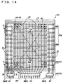
- FIG. 14 is a plan view illustrating an electro-optical device according to another embodiment of the present invention.
- FIG. 15 is a perspective view illustrating a device substrate that is a main portion of an electro-optical device shown in FIG. 14 .
- FIG. 16 is an enlarged plan view for a portion indicated by the arrow C of FIG. 14 .
- FIG. 17 is an enlarged plan view for a portion indicated by the arrow D of FIG. 14 .
- FIG. 18 is a graph illustrating data for determining the line width of electrode wirings in a portion indicated by the arrow E of FIG. 14 .
- FIG. 19 is a graph illustrating an experiment result.
- FIG. 1 illustrates an embodiment in which an electro-optical device according to the present invention is applied to a liquid crystal device that is an example thereof.
- the liquid crystal device mentioned herein which is an active matrix type using TFD (Thin Film Diode) being a two-terminal type switching element, is a transflective liquid crystal device using an device substrate as an electro-optical device substrate.
- FIG. 1 illustrates an embodiment in which an electro-optical device substrate according to the present invention is applied to a liquid crystal device.
- a liquid crystal device 1 comprises a liquid crystal panel 2 , a driver IC 3 mounted on the liquid crystal panel 2 , and an illuminating device 4 .
- the illuminating device 4 is disposed at the rear side of the liquid crystal panel 2 when viewed from the observing side (that is, the top of the drawing) and functions as a backlight.
- the illuminating device 4 may function as a front light by being disposed on the observing side of the liquid crystal panel 2 .
- the illuminating device 4 has a light source 6 comprising a point shape of a light source such as an LED (Light Emitting Diode), a linear shape of a light source such as a cold cathode tube, or the like, and a light guider 7 formed of a light-permeable resin.
- a reflective layer 8 is disposed on the rear side of the light guider 7 , if necessary.
- a diffusion layer 9 is disposed on the observing side of the light guider 7 , if necessary.
- a light inlet 7 a of the light guider 7 is extended in a direction perpendicular to a paper plane of FIG. 1 and light generated from the light source 6 is introduced into the light guider 7 via the light inlet 7 a.
- the liquid crystal panel 2 has a device substrate 12 as the electro-optical device substrate, a color filter substrate 11 as a counter substrate opposing it, and a square or rectangular shape frame type of a sealing member 13 when viewed in the direction of arrow A that bonds the substrates.
- a liquid crystal 14 is sealed in a gap surrounded by the substrates 11 and 12 and the sealing member 13 , so called a cell gap to configure a liquid crystal layer.
- the color filter substrate 11 has a first base 16 a of a rectangular or square shape as viewed in the direction of arrow A.
- a resin layer 17 having unevenness in other words, a combination of a concave portion and a non-concave portion is formed, and a reflective layer 18 is formed thereon.
- a colored layer 19 and a light-shielding layer 21 are formed thereon, and in turn an over coating layer 22 is formed thereon.
- An electrode 23 a extended in a linear manner is formed thereon in a direction perpendicular to the paper plane, and in turn an alignment film 24 a is formed thereon.
- the first base 16 a is formed of, for example, a light-permeable glass, a light-permeable plastic or the like.
- FIG. 2 is an enlarged view illustrating the vicinity of a display dot of FIG. 1 .
- the resin layer 17 is formed in a two-layer structure consisting of the first layer 17 a and the second layer 17 b , and small unevenness, in other words, a small concave portion and a small non-concave portion are formed on the surface of the second layer 17 b .
- the reflective layer 18 is formed of, for example, Al (aluminum), Al alloy or the like. A surface of this reflective layer 18 forms an uneven shape corresponding to the unevenness attached to the resin layer 17 being a bottom layer thereof. Light that is reflected to the reflective layer 18 is diffused by this uneven shape.
- FIG. 4 illustrates a plan structure viewed in the direction of arrow A in FIG. 2 .
- a colored layer 19 is formed of, for example, dots, each being a rectangular shape as shown in FIG. 4 , and a colored layer 19 represents one of three primary colors of R (red), G (green) and B (blue).
- the colored layer 19 of each color is disposed in a stripe arrangement, a delta arrangement, a mosaic arrangement, or any other appropriate arrangement.
- FIG. 4 illustrates the stripe arrangement.
- the colored layer 19 can be formed of three primary colors of C (Cyan), M (Magenta) and Y (Yellow).
- FIG. 2 is a cross-sectional view taken by an X—X line in FIG. 4 .
- the light-shielding layer 21 of FIG. 1 is formed of, for example, a light-shielding material, such as Cr (chrome) or the like, to fill among the plurality of colored layers 19 .
- This light-shielding layer 21 functions as a black matrix to improve a contrast of the image displayed by light that has transmitted through the colored layer 19 .
- the light-shielding layer 21 is not limited to being formed of a specific material, such as Cr or the like, but can be formed by overlapping, for example, respective colored layers of R, G, and B constituting the colored layer 19 , in other words, by a laminate.
- the over coating layer 22 is formed of, for example, a photosensitive resin such as an acryl resin, a polyimide resin or the like.
- a pass-through hole 28 is formed to a surface of the colored layer 19 in an appropriate place of the over coating layer 22 .
- a bottom hole in place of the pass-through hole 28 , a concave portion having a depth not to the surface of the colored layer 19 but into the over coating layer 22 can be formed in the over coating layer 22 .
- An electrode 23 a that is extended in a linear form in a direction perpendicular to the paper plane of FIG. 2 is formed of, for example, a metal oxide such as ITO (Indium Tin Oxide) or the like, and is inserted into the pass-through hole 28 at a portion of the center thereof.
- an alignment film 24 a formed thereon is formed of, for example, polyimide or the like, and the alignment film 24 a is also inserted into the pass-through hole 28 at a portion corresponding to the pass-through hole 28 . That is, a plurality of grooves is formed in the electrode 23 a and in the alignment film 24 a when viewed in plan in the direction of arrow A.
- the device substrate 12 opposing the color filter substrate 11 has the second base 16 b .
- this second base 16 b one side thereof where a protruding portion 29 is formed protrudes outside the first base 16 a .
- a plurality of TFDs 31 as a switching element is formed on an inner surface of the second base 16 b
- a plurality of dot electrodes 23 b is formed to be connected to the TFDs 31
- the alignment film 24 b is disposed thereon.
- the alignment of liquid crystal molecules around the second base 16 b is determined by applying an alignment process, for example, a rubbing process to the alignment film 24 b .
- a retardation film 26 b and a polarizer 27 b are mounted on an outer surface of the second base 16 b by adhesive or the like.
- the second base 16 b is formed of, for example, a light-permeable glass, a light-permeable plastic or the like.
- the dot electrode 23 b is formed of metal oxide such as ITO or the like.
- the alignment film 24 b is formed of, for example, polyimide or the like.
- FIG. 3 illustrates a cross-sectional view taken by the Z—Z line of FIG. 2 .
- An individual TFD 31 is disposed in the position corresponding to the light-shielding layer 21 at the color filter substrate 11 as shown in FIG. 3 .
- it is formed of the first TFD element 32 a and the second TFD element 32 b in serial connection.
- FIG. 3 is a cross-sectional view taken from the Y—Y line of FIG. 4 .
- TFD 31 as an example is formed as follows. That is, a first layer 34 a of the line wiring 33 and the first metal 36 of TFD 31 are first formed of TaW (tantalum tungsten). Next, a second layer 34 b of the line wiring 33 and an insulating film 37 of TFD 31 are formed in an anode oxide process. Then, a third layer 34 c of the line wiring 33 and the second metal 38 of the TFD device 31 are formed by Cr (chrome).
- the linear electrode 23 a formed on the color filter substrate 11 is extended along a left and right directions of a paper plane of the drawing.
- the above-stated line wiring 33 formed on the device substrate 12 is extended in a direction perpendicular to the linear electrode 23 a , in other words, in a direction perpendicular to the plane of the figure.
- the second metal 38 of the first TFD element 32 a is extended from the third layer 34 c of the line wiring 33 .
- a dot electrode 23 b is formed to overlap the front end of the second metal 38 of the second TFD element 32 b .
- a pair of TFD elements in an electrically opposite direction is interconnected in series between the first TFD element 32 a and the second TFD element 32 b .
- the structure is typically called a back-to-back structure, and it is known that the TFD device of this structure has a stable property as compared to a case where the TFD device is composed of only one TFD element.
- a bottom layer (not shown) may be disposed between the TFD 31 and the base 16 b , and between the line wiring 33 and the base 16 b.
- FIG. 6 illustrates a plan structure of a liquid crystal device 1 along arrow A of FIG. 1 .
- FIG. 6 illustrates an electrode and a wiring largely, and in the drawing, other elements are omitted.
- the second base 16 b constituting the device substrate 12 is indicated by a virtual line.
- a plurality of linear shape line wirings 33 is entirely disposed in the form of a stripe as shown in FIG. 7 .
- a plurality of TFDs 31 is connected to individual line wirings 33 with an appropriate gap, and a dot electrode 23 b is connected to the TFDs 31 .
- the line wiring 33 is schematically drawn by a small number of lines, in practice, many lines, for example about 240 lines are formed.
- the TFD 31 and the dot electrode 23 b corresponding to four edge portions of the sealing material 13 is shown in part, they are, in practice, disposed in the entire region surrounded by a sealing material 13 .
- a plurality of linear electrodes 23 a is entirely formed in the stripe form in the color filter substrate 11 opposing the device substrate 12 , as shown in FIG. 8 . These electrodes 23 a overlap a plurality of dot electrodes 23 b in a plan view, which are extended in a direction perpendicular to the line wiring 33 and forms a horizontal row when the device substrate 12 is bonded to the color filter substrate 11 by the sealing member 13 as shown in FIG. 6 .
- the region where the linear electrode 23 a and the dot electrode 23 b overlap each other forms a display dot, which is a minimum unit of the display.
- This display dot is a region indicated by a reference numeral D in FIGS. 1 to 4 .
- a region where a plurality of display dots D is arranged in a longitudinal direction and a horizontal direction in a matrix shape is a display region V.
- An image such as a character, a number, a figure or the like is displayed on this display region V.
- the driver IC 3 mounted on the protruding portion 29 of the second base 16 b constituting the device substrate 12 is composed of a driver IC 3 a for outputting a scanning signal, and a driver IC 3 b for outputting a data signal.
- External connection terminals 44 are formed in the first side 16 c of the second base 16 b , in other words, a side of the input, and the external connection terminals 44 are connected to the input terminal, for example, an input bump of the driver ICs 3 a and 3 b.
- a plurality of wirings 39 a is formed around two sides 16 d and 16 e adjacent to the first side 16 c along edges of the sides. These wirings 39 a are extended from output terminals, for example, output bumps of the driver ICs 3 a and 3 b toward the second side 16 f opposing the first side 16 c .
- Each wiring line 39 a is composed of a main line portion 49 a parallel with two sides 16 d and 16 e , respectively, and a portion 49 b that is bent in about 90° with respect to the main line portion.
- FIG. 9 is an enlarged view of wirings 39 a of a portion indicated by arrow B in FIG. 7 .
- a conductive pad 48 is formed in the front end of the bent portion 49 b of the wirings 39 a .
- the line width W 0 of the main line portion 49 a of the wirings 39 a is about 4 ⁇ m, and an interval ⁇ between the wirings is about 3 ⁇ m.
- the line width W 0 and the wiring gap ⁇ are uniform.
- the line width W 0 of the wirings 39 a through the front end of the bent portion 49 b from a point C where the main line portion 49 a is terminated, is slowly and continuously widened as it is spaced apart from the main line portion 49 a . Accordingly, the wiring resistance of the wirings 39 a is suppressed to be low.
- a spherical or cylindrical conductive material 42 is included in an irregular dispersion state inside the sealing member 13 .
- a pad 48 of the bent portion 49 b of the wirings 39 a at the device substrate 12 (see FIG. 9 ) and an end portion of the linear electrode 23 a at the color filter substrate 11 are conducted by the conductive material 42 .
- the electrode 23 a at the color filter substrate 11 is electrically connected to the driver IC 3 a via the wirings 39 a at the device substrate 12 .
- conduction of the linear electrode 23 a and the wirings 39 a are alternately realized between the left side and the right side in FIG. 6 .
- a driving method may be applied in which conduction of an upper half of the display region V is carried out in one of either a left side or a right side, and conduction of the lower half of the display region V is carried out in the other of either a left side or a right side.
- the line wiring 33 formed on the device substrate 12 is connected to the output terminal, for example, the output bump of the driver IC 3 b via the wiring 39 b formed on the same device substrate 12 .
- the wirings 39 a and 39 b are formed of elemental Cr, Cr/Ta (i.e., a laminated structure in which the first layer is Ta and the second layer is Cr), ITO/Cr/Ta (i.e., a laminated structure in which the first layer is Ta, the second layer is Cr, and the third layer is ITO), or the like. These wirings 39 a and 39 b can be simultaneously formed when the TFD 31 or the dot electrode 23 b is formed on the device substrate 12 .
- the driver IC 3 is mounted by ACF (Anisotropic Conductive Film) 43 .
- ACF 43 is formed by dispersing conductive particles in a thermosetting resin or ultraviolet setting resin.
- the body portion of the driver IC 3 is fixed on the protruding portion 29 of the substrate by the thermosetting resin or the like.
- the output bump of the driver IC 3 and the wirings 39 a and 39 b , and also the input bump of the driver IC 3 and an external connection terminal 44 are electrically connected by conductive particles included in the ACF 43 .
- a wiring substrate not shown, for example, a flexible wiring substrate is connected to the external connection terminal 44 by a conductive connection means such as soldering, ACF, heat seal or the like.
- a signal, a power or the like are supplied from an electronic apparatus, for example, a cellular phone or a portable information terminal to the liquid crystal device 1 via the wiring substrate.
- individual display dots D have substantially identical regions as that of the dot electrode 23 b .
- dot electrodes 23 b indicated by a dashed line are drawn to be slightly larger than the colored layer 19 indicated by a solid line, this is intended to easily show the structure in which, in practice, the plane shapes overlap one another in a substantially identical shape.
- each colored layer 19 of the dot shape is formed to correspond to each display dot D.
- openings 46 corresponding to respective display dots D are disposed in the reflective layer 18 .
- These openings 46 are formed in rectangular shapes in a plan view as shown in FIG. 4 .
- the openings 46 indicated by a broken line in FIG. 4 are drawn to be slightly larger than the pass-through hole 28 of the over-coating layer 22 indicated by a solid line, both edge thereof are substantially consistent in a plan view.
- one pixel is formed by three display dots D corresponding to three colored layers 19 , which correspond to the three colors of R, G, and B.
- one pixel is formed by one display dot D.
- a portion R where the reflective layer 18 is disposed is a reflecting portion
- a portion T in which the opening 46 is formed is a transmitting portion.
- External light incident from the observing side in other words, external light L 0 incident from the device substrate 12 (see FIG. 2 ) is reflected by the reflecting portion R.
- the light L 1 (see FIG. 2 ) emitted from the light guider 7 of the illuminating device 4 of FIG. 1 transmits through the transmitting portion T.
- the present embodiment configured as above, if external light such as sunlight, interior light or the like is intensive, the external light L 0 is reflected by the reflecting portion R toward the liquid crystal layer 14 . Accordingly, a reflective display is achieved.
- the illuminating device 4 of FIG. 1 when the illuminating device 4 of FIG. 1 is on, the light on the plane emitted from the light guider 7 is supplied to the liquid crystal layer 14 through the transmitting portion T of FIG. 2 . Accordingly, a transmissive display is achieved.
- a transflective display is achieved by optionally selecting and carrying out such reflective display and transmissive display.
- the linear electrode 23 a and the dot electrode 23 b exist with the liquid crystal layer 14 interposed between them, the linear electrode 23 a is applied with a scan signal in the present embodiment.
- the dot electrode 23 b is applied with the data signal in the present embodiment.
- a desired image such as a character, a number, a figure or the like, is displayed on an outer side of the device substrate 12 according to whether or not the modulated light passes through the polarizer 27 b of FIG. 1 .
- a case where the display is effected using external light L 0 is a reflective display
- a case where the display is effected using transmitted light L 1 is a transmissive display.
- the layer thickness E of the liquid crystal layer 14 in the transmission portion T is large and the layer thickness F in the reflecting portion R is small, uniform display quality is obtained between the reflective display and the transmissive display.
- the wirings 39 a are extended for the large distance along sides 16 d and 16 e of a second base 16 b constituting the device substrate 12 .
- the wirings 39 a . are extended over a large distance, wiring resistance increases and in turn crosstalk is generated. As a result, the display may be scattered.
- the wirings 39 a are provided with a portion whose line width W 0 gradually increases, the resistance of the wirings 39 a may decrease.
- the number of display dots D is as much as 320 ⁇ 240 in definition as in the present embodiment, the generation of the crosstalk can be prevented, and in turn the display is not scattered.
- the wirings 39 a as shown in FIG. 9 were used.
- the wirings 39 a have a portion whose line width increases in the bent portion 49 a .
- the portion whose line width is widened may be disposed at places other than the bent portion 49 b.
- the line width W 0 of the wirings 39 a is adapted to gradually increase in the bent portion 49 b .
- the wirings 39 a may be formed for the line width W 0 thereof to gradually increase step by step at the bent portion 49 b as shown in FIG. 10 .
- the present invention has been applied to the wirings 39 a formed on the device substrate 12 .
- the present invention may be applied to the wiring 39 b of FIG. 7 . Because the wiring 39 b has a short length, the wiring resistance would not decrease by intentionally applying the present invention.
- the present invention has been applied to the wirings 39 a formed on the device substrate 12 .
- the present invention may be applied to the wiring at the color filter substrate. That is, the color filter substrate 11 may be the electro-optical device substrate according to the present invention.
- the present invention has been applied to the liquid crystal device using TFD, it may be applied to an active matrix type liquid crystal device using a two-terminal type switching device rather than the TFD.
- the present invention may be applied to the active matrix type liquid crystal device using a three-terminal type switching device, such as TFT (Thin Film Transistor) or the like.
- the present invention may be applied to a simple matrix type liquid crystal device that does not use a switching device.
- the present invention may be applied to electro-optical devices in addition to the liquid crystal device, for example, an organic EL device, an inorganic EL device, a plasma display device (PDP), an electrophoretic display (EPD), and a field emission display device (FED).
- an organic EL device for example, an organic EL device, an inorganic EL device, a plasma display device (PDP), an electrophoretic display (EPD), and a field emission display device (FED).
- PDP plasma display device
- EPD electrophoretic display
- FED field emission display device
- FIG. 11 is a block diagram of an embodiment of the electronic apparatus.
- the electronic apparatus illustrated herein has a liquid crystal device 1 and a control means 80 for controlling the liquid crystal device 1 .
- the liquid crystal device 1 has a liquid crystal panel 81 and a driver circuit 82 composed of a semiconductor IC or the like.
- the control means 80 has a display information output source 83 , a display information processing circuit 84 , a power supply circuit 86 , and a timing generator 87 .
- the display information output source 83 has a memory composed of a ROM (Read Only Memory), a RAM (Random Access Memory) or the like; a storage unit such as a magnetic recording disk, optical recording disk or the like; and a tuning circuit for tuning outputting a digital image signal. It is composed to supply display information in the form of a predetermined format of a video signal or the like to the display information processing circuit 84 based on various clock signals produced by the timing generator 87 .
- the display information processing circuit 84 comprises known various circuits such as a serial-parallel converting circuit, an amplifying/inverting circuit, a rotation circuit, a gamma correcting circuit, a clamping circuit or the like to carry out inputted display information processing, so that the image information along with a clock signal (CLK) is supplied to the driver circuit 82 .
- the driver circuit 82 includes a scan line driver circuit, a data line driver circuit, and a checking circuit.
- the power supply circuit 86 supplies a predetermined voltage to each of the above-stated components.
- FIG. 12 illustrates an embodiment in which the present invention is applied to a cellular phone being an example of the electronic apparatus.
- the cellular phone 70 illustrated herein has a body portion 71 , and a display body portion 72 prepared therein in an open and close manner.
- the display device 73 composed of an electro-optical device, such as the liquid crystal device or the like, is disposed in the display body portion 72 , which enables visual confirmation of various displays regarding phone communication through the display screen 74 at the display body portion 72 .
- An operation button 76 is arranged and prepared at the front face of the body portion 71 .
- a retractable antenna 77 is mounted to one end of the display body portion 72 .
- a speaker is disposed inside the earpiece 78 while a microphone is mounted inside a mouthpiece 79 .
- a control unit for controlling the operation of the display device 73 is included in the body portion 71 or the display body portion 72 as a portion of a control unit responsible for a control of the entire cellular phone, or separately from the control unit.
- FIG. 13 illustrates an embodiment in which the present invention is applied to a portable information device being another example of the electronic apparatus.
- a portable information device 90 illustrated herein is an information device having a touch panel, and has a liquid crystal device 91 as an electro-optical device.
- the information device 90 has a display region V composed of a display plane of the liquid crystal device 91 , and a first input region W 1 positioned beneath the display region V.
- An input sheet 92 is disposed at the first input region W 1 .
- the liquid crystal device 91 has a structure in which a liquid crystal panel has a rectangular or square shape and a touch panel has the same rectangular or square shape overlap in a plan view.
- the touch panel functions as an input panel.
- the touch panel is larger than the liquid crystal panel and has a shape protruded from an end of the liquid crystal panel.
- a region corresponding to the display region V also functions as a second input region W 2 that can be input-operated like the first input region W 1 .
- the touch panel has a second face positioned at the liquid crystal panel and a first face opposing it, and an input sheet 92 is attached at a position corresponding to the first input region W 1 of the first face.
- a frame for identifying an icon 93 and a self-scripted character recognition region W 3 is printed on the input sheet 92 .
- the input sheet 92 For the first input region W 1 , since a load from an input means such as a finger or a pen is applied on the first face of the touch panel through the input sheet 92 , selection of the icon 93 or data input, such as character input in the character recognition region W 3 or the like, can be carried out.
- the image on the liquid crystal panel can be viewed and also, for example, an input mode screen may be displayed on the liquid crystal panel, and a load of a finger or a pen is applied on the first face of the touch panel.
- an input mode screen may be displayed on the liquid crystal panel, and a load of a finger or a pen is applied on the first face of the touch panel.
- An electronic apparatus may include, for example, a personal computer, a liquid crystal TV, a digital still camera, a wrist watch, a viewfinder or a monitor direct type video tape recorder, a car navigation device, a pager, an electronic organizer, a calculator, a word processor, a workstation, a TV phone, a POS terminal, and other devices, in addition to the above-stated cellular phone or portable information device.
- FIG. 14 illustrates a plan structure of a liquid crystal device 101 being an embodiment of the present invention.
- FIG. 15 illustrates a plan structure of a device substrate 112 used in the liquid crystal device 101 of FIG. 14 .
- the configuration of the counter substrate 111 opposing the device substrate 112 is basically the same as that of the embodiment shown in FIG. 8 , but the front end configuration of the linear electrode 23 a is rather different, as described below.
- FIGS. 14 and 15 since the members identical to those in the embodiment shown in FIG. 6 use similar reference numerals, explanation thereof will be omitted.
- a plurality of entire wirings 39 a disposed on the device substrate 112 is accommodated in a region surrounded by the sealing member 13 .
- the front end of the electrode wirings 25 extended from the linear electrode 23 a disposed on the color filter substrate 111 being the counter substrate is electrically connected to a front end of the wirings 39 a at the device substrate 112 , in other words, the front end of the bent portion 49 b by the conductive material 42 included in the sealing member 13 .
- FIG. 16 is an enlarged view of a region indicated by arrow C of FIG. 14 .
- the electrode wirings 25 are wirings that are extended from the linear electrode 23 a to an outer side of the display region V.
- FIG. 17 is an enlarged view of a region of arrow D of FIG. 14 . That is, FIG. 17 illustrates a structure of another end of the wiring structure shown in FIG. 16 .
- terminals 40 are formed in respective other ends of the plurality of wirings 39 a , and these terminals 40 are connected to an output bump (not shown) of the driver IC 3 a by ACF (Anisotropic Conductive Film) or other conductive connection members.
- ACF Application Functional Conductive Film
- the wiring width increases in the bent portion 49 b of the wirings 39 a as shown in FIG. 16 .
- an area of the wirings increases as the length of the wirings increases. Accordingly, uniformity of the wiring resistance among the plurality of wirings 39 a is realized by preventing high resistance of the long wiring.
- the wiring width of the entire wirings 39 a is getting larger.
- the wirings 39 a when viewing the plurality of wirings 39 a formed on the left side 16 e in FIG. 15 , the wirings 39 a have the shortest length at the left and the longest length at the right. In FIGS.
- This configuration is the same for a plurality of wirings 39 a formed on the right side 16 d of FIG. 15 .
- the wiring width is varied in response to the wiring length, the wiring resistance among the plurality of wirings 39 a can become more uniform.
- a plurality of linear electrodes 23 a is formed in the stripe shape on the counter substrate 11 shown in FIG. 14 .
- the electrode wirings 25 are extended from the electrodes 23 a .
- These electrode wirings 25 are electrically connected to front ends of the plurality of wirings 39 a on the device substrate, in other words, the pad 48 by a conductive material 42 distributed in the sealing member 13 of FIG. 14 , respectively.
- the plurality of electrode wirings 25 is formed to increase in respective widths W 1 , W 2 , W 3 , . . .
- n is the number of the wirings 39 a
- the wirings 39 a increase in length. Accordingly, in FIG. 14 , it is possible to make the entire wiring resistance of the wirings 39 a from the driver IC 3 a to the linear electrode 23 a and the electrode wirings 25 uniform among the plurality of electrodes 23 a.
- the wirings 39 a in this region are very short in length and low in resistance. There is a limitation in raising the resistance value. Accordingly, if only the line width of the wirings 39 a of the device substrate is adjusted, the wiring resistance decreases and is not uniform in a region having a short length of wirings, in other words, a region having a small value in the wiring width direction X, as represented by a reference numeral F in FIG. 18 . In order to overcome this phenomenon, in the present embodiment, in a wiring width region of FIG.
- the line width (corresponding to W 1 to Wn of FIG. 16 ) of the electrode wirings 25 at the counter substrate is thinned to raise a resistance value, and this results in the wiring resistance being set to be uniform for all wirings 39 a , as indicated by the reference numeral G. Accordingly, a clear display having no irregularity can be obtained.
- a liquid crystal device in which the line widths of all wirings 39 a are uniform regardless of the length of the wirings 39 a in the liquid crystal device 1 of FIG. 6 (hereinafter, referred to as a conventional product).
- a liquid crystal device in which (a) the line width of the plurality of wirings 39 a increases to the bent portion 49 b , as shown in FIG. 16 , (b) as the length of the wirings 39 a increase, the entire wiring width dn of the wirings 39 a including the main line portion increases, as shown in FIGS. 16 and 17 , and (c) for the wirings 39 a having a short length in a region indicated by arrow E of FIG. 14 , the width of the wiring electrode 25 at the counter substrate is not adjusted to be small in the liquid crystal device 101 of FIG. 14 (hereinafter, referred to as a product of invention B).
- the wiring width adjustment in (b) was performed as shown in FIG. 19( a ). Specifically, a small side of the wiring width direction X (i.e., a short side in the wiring length) is set to a minimum width “3 ⁇ m”, and the wiring width increases to a maximum “7.6 ⁇ m”.
- FIG. 19( b ) The wiring resistance from the driver IC 3 a to the linear electrode 23 a in FIGS. 6 and 14 was measured for the three types of the liquid crystal devices. As a result, a result shown in FIG. 19( b ) could be obtained.
- a reference numeral H denotes the wiring resistance of the conventional product
- a reference numeral I denotes the wiring resistance of the product according to invention A
- a reference numeral J denotes the wiring resistance of the product according to invention B.
- slowly increasing the line width of the wirings 39 a allows considerable uniformity of the wiring resistance.
- An electro-optical device substrate according to the present invention is very suitable for use as a substrate for a liquid crystal device, an organic EL device or the like.
- the electro-optical device according to the present invention is very suitable for use upon uniform display without irregularities in the liquid crystal device, the organic EL device or the like.
- an electronic apparatus according to the present invention is very suitable for use upon the uniform display without irregularities on a cellular phone, a portable information terminal, PDA or the like.
Abstract
Description
Claims (18)
Applications Claiming Priority (4)
| Application Number | Priority Date | Filing Date | Title |
|---|---|---|---|
| JP2003-014733 | 2003-01-23 | ||
| JP2003014733 | 2003-01-23 | ||
| JP2003377171A JP3925486B2 (en) | 2003-01-23 | 2003-11-06 | Electro-optical device substrate, electro-optical device, and electronic apparatus |
| JP2003-377171 | 2003-11-06 |
Publications (2)
| Publication Number | Publication Date |
|---|---|
| US20040189915A1 US20040189915A1 (en) | 2004-09-30 |
| US7068338B2 true US7068338B2 (en) | 2006-06-27 |
Family
ID=32992889
Family Applications (1)
| Application Number | Title | Priority Date | Filing Date |
|---|---|---|---|
| US10/764,607 Active 2024-04-18 US7068338B2 (en) | 2003-01-23 | 2004-01-23 | Electro-optical device substrate, electro-optical device, and electronic apparatus |
Country Status (5)
| Country | Link |
|---|---|
| US (1) | US7068338B2 (en) |
| JP (1) | JP3925486B2 (en) |
| KR (1) | KR100590984B1 (en) |
| CN (1) | CN100343744C (en) |
| TW (1) | TWI287656B (en) |
Cited By (6)
| Publication number | Priority date | Publication date | Assignee | Title |
|---|---|---|---|---|
| US20070030409A1 (en) * | 2005-08-08 | 2007-02-08 | Mitsubishi Denki Kabushiki Kaisha | Liquid crystal display device |
| US20070241349A1 (en) * | 2006-04-14 | 2007-10-18 | Toshiki Kishioka | Semiconductor device with a driver circuit for light emitting diodes |
| US20090257015A1 (en) * | 2006-07-27 | 2009-10-15 | Rohm Co., Ltd. | Image display |
| US8360600B2 (en) | 2010-05-04 | 2013-01-29 | Au Optronics Corp. | Electronic illuminating device |
| US10991728B2 (en) * | 2018-11-26 | 2021-04-27 | Au Optronics Corporation | Display panel |
| US11915652B2 (en) | 2015-02-12 | 2024-02-27 | Samsung Display Co., Ltd. | Non-quadrangular display |
Families Citing this family (15)
| Publication number | Priority date | Publication date | Assignee | Title |
|---|---|---|---|---|
| JP4357389B2 (en) * | 2004-08-20 | 2009-11-04 | 富士通株式会社 | Touch panel device and manufacturing method thereof |
| KR100700653B1 (en) * | 2005-02-03 | 2007-03-27 | 삼성에스디아이 주식회사 | Organic Electro Luminescence Display |
| JP2006234918A (en) * | 2005-02-22 | 2006-09-07 | Hitachi Displays Ltd | Display apparatus |
| JP4534972B2 (en) * | 2005-03-30 | 2010-09-01 | エプソンイメージングデバイス株式会社 | Electro-optical device and electronic apparatus |
| US7710739B2 (en) * | 2005-04-28 | 2010-05-04 | Semiconductor Energy Laboratory Co., Ltd. | Semiconductor device and display device |
| KR100775827B1 (en) * | 2005-12-22 | 2007-11-13 | 엘지전자 주식회사 | Organic electroluminescent device |
| KR101581245B1 (en) * | 2009-09-16 | 2015-12-31 | 엘지디스플레이 주식회사 | Organic Electroluminescent Display Device |
| JP5471317B2 (en) | 2009-11-05 | 2014-04-16 | 日本精機株式会社 | Organic EL panel |
| JP5991709B2 (en) * | 2012-05-01 | 2016-09-14 | 株式会社ジャパンディスプレイ | LCD with built-in touch panel |
| JP6112544B2 (en) * | 2012-11-27 | 2017-04-12 | 国立大学法人電気通信大学 | Electrode substrate for tactile presentation device, tactile presentation device, and display device |
| CN103424901A (en) | 2013-08-19 | 2013-12-04 | 京东方科技集团股份有限公司 | Display panel and display module |
| JP2017009716A (en) * | 2015-06-18 | 2017-01-12 | 株式会社ジャパンディスプレイ | Display device |
| KR102476563B1 (en) * | 2015-12-01 | 2022-12-12 | 엘지디스플레이 주식회사 | Display device |
| TWI602002B (en) * | 2016-11-30 | 2017-10-11 | 友達光電股份有限公司 | Display panel |
| KR20200086770A (en) | 2019-01-09 | 2020-07-20 | 삼성디스플레이 주식회사 | Organic light emitting diode display device |
Citations (10)
| Publication number | Priority date | Publication date | Assignee | Title |
|---|---|---|---|---|
| KR960011489A (en) | 1994-09-08 | 1996-04-20 | 카나이 쯔또무 | LCD Display |
| JPH117039A (en) | 1997-06-17 | 1999-01-12 | Hitachi Ltd | Liquid crystal display element |
| JP2000056699A (en) | 1998-08-03 | 2000-02-25 | Nec Corp | Layout method of lead-out wiring and display device having high density wiring |
| US6327443B1 (en) * | 1994-11-08 | 2001-12-04 | Citizen Watch Co., Ltd. | Liquid crystal display device |
| JP2002040475A (en) | 2001-06-13 | 2002-02-06 | Hitachi Ltd | Liquid crystal display device |
| JP2002148654A (en) | 2000-11-14 | 2002-05-22 | Seiko Epson Corp | Liquid crystal display device |
| JP2002229009A (en) | 2001-02-06 | 2002-08-14 | Seiko Epson Corp | Liquid crystal display and electronic device |
| JP2002350892A (en) | 2001-03-22 | 2002-12-04 | Citizen Watch Co Ltd | Liquid crystal display device |
| US6888606B2 (en) * | 2001-04-16 | 2005-05-03 | Seiko Epson Corporation | Electrooptic device and electronic apparatus |
| US6917408B2 (en) * | 2001-11-30 | 2005-07-12 | Sharp Kabushiki Kaisha | Display panel |
Family Cites Families (1)
| Publication number | Priority date | Publication date | Assignee | Title |
|---|---|---|---|---|
| JP2002268079A (en) * | 2001-03-09 | 2002-09-18 | Seiko Epson Corp | Optoelectronic device and electronic apparatus |
-
2003
- 2003-11-06 JP JP2003377171A patent/JP3925486B2/en not_active Expired - Lifetime
-
2004
- 2004-01-17 KR KR1020040003520A patent/KR100590984B1/en active IP Right Grant
- 2004-01-19 TW TW093101386A patent/TWI287656B/en not_active IP Right Cessation
- 2004-01-20 CN CNB2004100004460A patent/CN100343744C/en not_active Expired - Lifetime
- 2004-01-23 US US10/764,607 patent/US7068338B2/en active Active
Patent Citations (12)
| Publication number | Priority date | Publication date | Assignee | Title |
|---|---|---|---|---|
| KR960011489A (en) | 1994-09-08 | 1996-04-20 | 카나이 쯔또무 | LCD Display |
| US5757450A (en) | 1994-09-08 | 1998-05-26 | Hitachi, Ltd. | Liquid crystal display with color filters and sizes of inclined linear wiring and terminal electrodes adjusted for equal resistances |
| US5914763A (en) | 1994-09-08 | 1999-06-22 | Hitachi, Ltd. | Liquid crystal display with substantially equal resistances for sets of terminal electrodes and inclined wiring electrodes |
| US6327443B1 (en) * | 1994-11-08 | 2001-12-04 | Citizen Watch Co., Ltd. | Liquid crystal display device |
| JPH117039A (en) | 1997-06-17 | 1999-01-12 | Hitachi Ltd | Liquid crystal display element |
| JP2000056699A (en) | 1998-08-03 | 2000-02-25 | Nec Corp | Layout method of lead-out wiring and display device having high density wiring |
| JP2002148654A (en) | 2000-11-14 | 2002-05-22 | Seiko Epson Corp | Liquid crystal display device |
| JP2002229009A (en) | 2001-02-06 | 2002-08-14 | Seiko Epson Corp | Liquid crystal display and electronic device |
| JP2002350892A (en) | 2001-03-22 | 2002-12-04 | Citizen Watch Co Ltd | Liquid crystal display device |
| US6888606B2 (en) * | 2001-04-16 | 2005-05-03 | Seiko Epson Corporation | Electrooptic device and electronic apparatus |
| JP2002040475A (en) | 2001-06-13 | 2002-02-06 | Hitachi Ltd | Liquid crystal display device |
| US6917408B2 (en) * | 2001-11-30 | 2005-07-12 | Sharp Kabushiki Kaisha | Display panel |
Non-Patent Citations (1)
| Title |
|---|
| Korean examination report dated Oct. 31, 2005. |
Cited By (10)
| Publication number | Priority date | Publication date | Assignee | Title |
|---|---|---|---|---|
| US20070030409A1 (en) * | 2005-08-08 | 2007-02-08 | Mitsubishi Denki Kabushiki Kaisha | Liquid crystal display device |
| US7525625B2 (en) * | 2005-08-08 | 2009-04-28 | Mitsubishi Denki Kabushiki Kaisha | Liquid crystal display device comprising a common signal line overlapping a sealing member and including at least two conductive layers with at least one of the conductive layers changing a pattern width |
| US20090174856A1 (en) * | 2005-08-08 | 2009-07-09 | Mitsubishi Denki Kabushiki Kaisha | Liquid crystal display device |
| US8031318B2 (en) | 2005-08-08 | 2011-10-04 | Mitsubishi Denki Kabushiki Kaisha | Liquid crystal display device |
| US20070241349A1 (en) * | 2006-04-14 | 2007-10-18 | Toshiki Kishioka | Semiconductor device with a driver circuit for light emitting diodes |
| US8013348B2 (en) * | 2006-04-14 | 2011-09-06 | Ricoh Company, Ltd. | Semiconductor device with a driver circuit for light emitting diodes |
| US20090257015A1 (en) * | 2006-07-27 | 2009-10-15 | Rohm Co., Ltd. | Image display |
| US8360600B2 (en) | 2010-05-04 | 2013-01-29 | Au Optronics Corp. | Electronic illuminating device |
| US11915652B2 (en) | 2015-02-12 | 2024-02-27 | Samsung Display Co., Ltd. | Non-quadrangular display |
| US10991728B2 (en) * | 2018-11-26 | 2021-04-27 | Au Optronics Corporation | Display panel |
Also Published As
| Publication number | Publication date |
|---|---|
| TW200424644A (en) | 2004-11-16 |
| JP2004246330A (en) | 2004-09-02 |
| CN100343744C (en) | 2007-10-17 |
| KR20040067941A (en) | 2004-07-30 |
| JP3925486B2 (en) | 2007-06-06 |
| TWI287656B (en) | 2007-10-01 |
| US20040189915A1 (en) | 2004-09-30 |
| KR100590984B1 (en) | 2006-06-19 |
| CN1517762A (en) | 2004-08-04 |
Similar Documents
| Publication | Publication Date | Title |
|---|---|---|
| US7068338B2 (en) | Electro-optical device substrate, electro-optical device, and electronic apparatus | |
| US6888606B2 (en) | Electrooptic device and electronic apparatus | |
| US7167227B2 (en) | Electrooptic device, driving IC, and electronic apparatus | |
| US8009253B2 (en) | Electro-optical device having insulating layer with varying thickness in the reflection and transmission displays | |
| US6999151B2 (en) | Electro-optical device, electronic apparatus, and method of manufacturing the electro-optical device | |
| US7202508B2 (en) | Electro-optical device and electronic apparatus device | |
| US6992737B2 (en) | Color filter substrate, electrooptic device and electronic apparatus, and methods for manufacturing color filter substrate and electrooptic device | |
| US6927831B2 (en) | Liquid crystal device and electronic apparatus having a substantially uniform substrate interval | |
| JP4453434B2 (en) | Liquid crystal device and electronic device | |
| US20080170016A1 (en) | Liquid crystal device, method for driving the liquid crystal device and electronic equipment | |
| JP2004258365A (en) | Electrooptical device and electronic apparatus using it | |
| JP2005208129A (en) | Liquid crystal apparatus and electronic device | |
| JP2006234871A (en) | Liquid crystal apparatus and electronic equipment | |
| JP2007065602A (en) | Liquid crystal device and electronic apparatus | |
| JP3649222B2 (en) | Liquid crystal device and electronic device | |
| JP2004226712A (en) | Mother substrate for electrooptical device, substrate for electrooptical device, electrooptical device and its manufacturing method, and electronic equipment | |
| JP4645327B2 (en) | Liquid crystal display device and electronic device | |
| JP2005284296A (en) | Electrooptical device and electronic apparatus | |
| JP2006003808A (en) | Liquid crystal apparatus and electronic device | |
| JP2006091062A (en) | Optoelectronic device, manufacturing method for optoelectronic device, and electronic equipment | |
| JP2005284055A (en) | Liquid crystal display and electronic equipment | |
| JP2005292223A (en) | Electro-optical device and electronic equipment | |
| JP2005195744A (en) | Substrate for electrooptical device, electrooptical device, method for manufacturing electrooptical device, and electronic equipment | |
| JP2007264252A (en) | Liquid crystal device and electronic equipment | |
| JP2006189671A (en) | Liquid crystal apparatus and electronic device |
Legal Events
| Date | Code | Title | Description |
|---|---|---|---|
| AS | Assignment |
Owner name: SEIKO EPSON CORPORATION, JAPAN Free format text: ASSIGNMENT OF ASSIGNORS INTEREST;ASSIGNORS:TAGUCHI, SATOSHI;MIYAKO, YUICHIRO;KANEKO, HIDEKI;REEL/FRAME:015406/0075;SIGNING DATES FROM 20040517 TO 20040518 |
|
| STCF | Information on status: patent grant |
Free format text: PATENTED CASE |
|
| FEPP | Fee payment procedure |
Free format text: PAYOR NUMBER ASSIGNED (ORIGINAL EVENT CODE: ASPN); ENTITY STATUS OF PATENT OWNER: LARGE ENTITY |
|
| FPAY | Fee payment |
Year of fee payment: 4 |
|
| FPAY | Fee payment |
Year of fee payment: 8 |
|
| AS | Assignment |
Owner name: INTELLECTUALS HIGH-TECH KFT, HUNGARY Free format text: ASSIGNMENT OF ASSIGNORS INTEREST;ASSIGNOR:SEIKO EPSON CORPORATION;REEL/FRAME:039300/0295 Effective date: 20160524 Owner name: SHENZHEN CHINA STAR OPTOELECTRONICS TECHNOLOGY CO. Free format text: ASSIGNMENT OF ASSIGNORS INTEREST;ASSIGNOR:INTELLECTUALS HIGH-TECH KFT;REEL/FRAME:039301/0043 Effective date: 20160512 |
|
| FEPP | Fee payment procedure |
Free format text: PAYER NUMBER DE-ASSIGNED (ORIGINAL EVENT CODE: RMPN); ENTITY STATUS OF PATENT OWNER: LARGE ENTITY Free format text: PAYOR NUMBER ASSIGNED (ORIGINAL EVENT CODE: ASPN); ENTITY STATUS OF PATENT OWNER: LARGE ENTITY |
|
| MAFP | Maintenance fee payment |
Free format text: PAYMENT OF MAINTENANCE FEE, 12TH YEAR, LARGE ENTITY (ORIGINAL EVENT CODE: M1553) Year of fee payment: 12 |