JP4423458B2 - Control method of DC / DC converter - Google Patents
Control method of DC / DC converter Download PDFInfo
- Publication number
- JP4423458B2 JP4423458B2 JP2001074656A JP2001074656A JP4423458B2 JP 4423458 B2 JP4423458 B2 JP 4423458B2 JP 2001074656 A JP2001074656 A JP 2001074656A JP 2001074656 A JP2001074656 A JP 2001074656A JP 4423458 B2 JP4423458 B2 JP 4423458B2
- Authority
- JP
- Japan
- Prior art keywords
- transformer
- negative
- voltage
- power supply
- positive
- Prior art date
- Legal status (The legal status is an assumption and is not a legal conclusion. Google has not performed a legal analysis and makes no representation as to the accuracy of the status listed.)
- Expired - Fee Related
Links
Images


Classifications
-
- H—ELECTRICITY
- H02—GENERATION; CONVERSION OR DISTRIBUTION OF ELECTRIC POWER
- H02M—APPARATUS FOR CONVERSION BETWEEN AC AND AC, BETWEEN AC AND DC, OR BETWEEN DC AND DC, AND FOR USE WITH MAINS OR SIMILAR POWER SUPPLY SYSTEMS; CONVERSION OF DC OR AC INPUT POWER INTO SURGE OUTPUT POWER; CONTROL OR REGULATION THEREOF
- H02M1/00—Details of apparatus for conversion
- H02M1/08—Circuits specially adapted for the generation of control voltages for semiconductor devices incorporated in static converters
- H02M1/083—Circuits specially adapted for the generation of control voltages for semiconductor devices incorporated in static converters for the ignition at the zero crossing of the voltage or the current
-
- H—ELECTRICITY
- H02—GENERATION; CONVERSION OR DISTRIBUTION OF ELECTRIC POWER
- H02M—APPARATUS FOR CONVERSION BETWEEN AC AND AC, BETWEEN AC AND DC, OR BETWEEN DC AND DC, AND FOR USE WITH MAINS OR SIMILAR POWER SUPPLY SYSTEMS; CONVERSION OF DC OR AC INPUT POWER INTO SURGE OUTPUT POWER; CONTROL OR REGULATION THEREOF
- H02M3/00—Conversion of dc power input into dc power output
- H02M3/22—Conversion of dc power input into dc power output with intermediate conversion into ac
- H02M3/24—Conversion of dc power input into dc power output with intermediate conversion into ac by static converters
- H02M3/28—Conversion of dc power input into dc power output with intermediate conversion into ac by static converters using discharge tubes with control electrode or semiconductor devices with control electrode to produce the intermediate ac
- H02M3/325—Conversion of dc power input into dc power output with intermediate conversion into ac by static converters using discharge tubes with control electrode or semiconductor devices with control electrode to produce the intermediate ac using devices of a triode or a transistor type requiring continuous application of a control signal
- H02M3/335—Conversion of dc power input into dc power output with intermediate conversion into ac by static converters using discharge tubes with control electrode or semiconductor devices with control electrode to produce the intermediate ac using devices of a triode or a transistor type requiring continuous application of a control signal using semiconductor devices only
- H02M3/33569—Conversion of dc power input into dc power output with intermediate conversion into ac by static converters using discharge tubes with control electrode or semiconductor devices with control electrode to produce the intermediate ac using devices of a triode or a transistor type requiring continuous application of a control signal using semiconductor devices only having several active switching elements
- H02M3/33571—Half-bridge at primary side of an isolation transformer
-
- H—ELECTRICITY
- H02—GENERATION; CONVERSION OR DISTRIBUTION OF ELECTRIC POWER
- H02M—APPARATUS FOR CONVERSION BETWEEN AC AND AC, BETWEEN AC AND DC, OR BETWEEN DC AND DC, AND FOR USE WITH MAINS OR SIMILAR POWER SUPPLY SYSTEMS; CONVERSION OF DC OR AC INPUT POWER INTO SURGE OUTPUT POWER; CONTROL OR REGULATION THEREOF
- H02M3/00—Conversion of dc power input into dc power output
- H02M3/01—Resonant DC/DC converters
Description
【0001】
【発明の属する技術分野】
この発明は、ハーフブリッジ構成のDC/DCコンバータ、特にその制御方法に関する。
【0002】
【従来の技術】
図6に従来例を示す。
【0003】
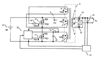
同図に示すように、直流電源10と並列にMOSFET(金属酸化物半導体電界効果トランジスタ)1とMOSFET2との直列回路を接続し、コンデンサ3と変圧器1次巻線5との直列回路とスナバコンデンサ21を、MOSFET2にそれぞれ並列に接続して構成される。変圧器22の2次側には2つの巻線8,9を備え、ダイオード12,13とコンデンサ14からなる整流平滑回路を有している。また、平滑された直流出力電圧を一定に保つため、出力電圧検出回路17と周波数・位相制御回路19を設け、フィードバック制御を行なうようにしている。また、MOSFET1,2の各ゲートを駆動する回路には、高耐圧ドライバIC(集積回路)20が用いられている。
【0004】
図7に図6のタイミングチャートを示す。以下、その動作について図6も参照して説明する。
【0005】
まず、期間(1)においてMOSFET1をオンすることにより、直流電源10→コンデンサ3→変圧器1次巻線5→MOSFET1を介して、コンデンサ3と変圧器22の漏れインダクタンスによる共振電流と変圧器22の励磁電流が流れ、コンデンサ3が充電される。このとき、変圧器1次巻線5には直流電源電圧Edとコンデンサ3との差電圧VP1が印加され、変圧器2次巻線8に発生する電圧VS1をダイオード12,コンデンサ14により整流,平滑し負荷に電力を供給する。変圧器2次巻線電圧VS1は、変圧器1次巻線電圧VP1の巻数比に比例した電圧(図7中に点線で示す)で上昇し、出力電圧Voに達するとダイオード12が導通し、出力電圧Voにクランプされる。図中の点線と実線の差電圧は、変圧器22の漏れインダクタンスに印加される。
【0006】
期間(2)において変圧器1次巻線電圧VP1は徐々に低下し、変圧器1次巻線電圧VP1の巻数比に比例した電圧が出力電圧Voよりも下回ると、ダイオード12は阻止状態となり電流が零となる。また、MOSFET1には期間(1)で励磁された変圧器22の励磁電流が継続して流れる。
【0007】
期間(3)において、MOSFET1をオフすることにより、変圧器22の励磁電流はスナバコンデンサ21およびMOSFET1,2の出力容量に転流し、MOSFET1,2の電圧は徐々に上昇または下降する。
【0008】
期間(4)において、MOSFET1の電圧が直流電源電圧Edに達すると、変圧器22の励磁電流はMOSFET2の寄生ダイオードに転流する。このとき、MOSFET2をオンすることにより、コンデンサ3→MOSFET2→変圧器1次巻線5を介して共振電流と変圧器22の励磁電流が流れ、コンデンサ3を放電する。また、変圧器1次巻線5には直流電源電圧Edとコンデンサ3との差電圧VP1が印加され、変圧器22はリセットされる。また、このとき変圧器2次巻線9に発生する電圧をダイオード13,コンデンサ14により整流,平滑し負荷に電力を供給する。
【0009】
以下、期間(4)から(6)の動作は期間(1)から(3)と同様なので、説明は省略する。
【0010】
こうして、期間(1)から(6)の一連の動作を繰り返すことにより、直流電源10から負荷に電力が供給される。
【0011】
次に、軽負荷時の動作を図8を参照して説明する。
【0012】
軽負荷時には、スイッチング周波数が増大しないように周波数・位相制御回路19を調整し、変圧器2次側電流ID12,ID13が零になった時点より或る時間が経過してから、MOSFET1またはMOSFET2をオフする。MOSFET1,2に流れる電流IQ1,2は、変圧器22の励磁電流にほぼ等しくなる。
【0013】
【発明が解決しようとする課題】
上記の従来例では、各MOSFETは定格負荷から無負荷までデューティ(duty)50%で交互にスイッチングし、負荷の変化に対して出力電圧検出回路および周波数・位相制御回路を用いて、変圧器1次巻線に印加される電圧を調整して負荷に供給する電流を制御することにより、出力電圧を一定にしている。
【0014】
しかし、この方法では、定格負荷から無負荷まで変圧器の励磁インダクタンスに流れる励磁電流の値がほとんど変化しないため、この励磁電流が無効電流となり、回路中のインピーダンス(MOSFETのオン抵抗,トランスの巻線抵抗など)によって損失が発生し、結果的に軽負荷時の効率が低下するという問題がある。
【0015】
また、直流電源の正極に接続されるMOSFETのソース端子の電位が、直流電源の負極に接続されたMOSFETのソース端子の電位とは異なるため、正極側のMOSFETを駆動する信号はパルストランスなどで絶縁するか、またはレベルシフト機能を持った高価な高耐圧ドライバICが必要となり、装置の大型化やコストアップを招くことになる。
【0016】
したがって、この発明の課題は、無効電流を低く抑え、高価な部品を不要としてコストを低減することにある。
【0017】
【課題を解決するための手段】
このような課題を解決するため、請求項1の発明では、直流電源の正極と負極間に並列に2つのスイッチ素子の直列回路を接続するとともに、少なくとも1つのコンデンサと変圧器1次巻線との直列回路を前記スイッチ素子の一方に並列に接続し、前記直流電源の正極側に接続したスイッチ素子には前記変圧器の3次巻線からオンオフ信号を与える一方、変圧器の4次巻線は制御回路の電源用として用い、かつ、この制御回路により4次巻線電圧の正負の切替りのタイミングを検出し、そのタイミングで直流電源の負極側に接続したスイッチ素子にオンオフ信号を与えることにより、変圧器の2次巻線に発生する正負の電圧を半波または全波整流して直流出力を得るDC/DCコンバータにおいて、
前記直流電源の負極側に接続したスイッチ素子は、変圧器4次巻線の電圧の正から負または負から正への切替りから短絡防止期間を経た後にオンとし、前記スイッチ素子のオンまたは変圧器4次巻線の電圧の切替りタイミングから時間に比例して増加する参照電圧値を2次側出力電圧検出値と比較し、この電圧検出値に対して前記参照電圧値が上回ったとき、前記スイッチ素子をオフさせることにより、直流出力電圧を一定とするとともに、前記2次側出力電圧検出値が前記参照電圧を上回ったことを検出したときは、或る一定の周波数で発振する矩形波信号の立ち上がりまたは立ち下がりのタイミングで、前記スイッチ素子に駆動信号を与えることにより、前記DC/DCコンバータの誤停止を防止することを特徴とする。
この請求項1の発明においては、前記参照電圧の最小値が前記2次側出力電圧検出値の最小値よりも大きくなるように、一定のオフセットを持たせることができる(請求項2の発明)。
【0018】
請求項3の発明では、直流電源の正極と負極間に並列に2つのスイッチ素子の直列回路を接続するとともに、少なくとも1つのコンデンサと変圧器1次巻線との直列回路を前記スイッチ素子の一方に並列に接続し、前記直流電源の正極側に接続したスイッチ素子には前記変圧器の3次巻線からオンオフ信号を与える一方、変圧器の4次巻線は制御回路の電源用として用い、かつ、この制御回路により4次巻線電圧の正負の切替りのタイミングを検出し、そのタイミングで直流電源の負極側に接続したスイッチ素子にオンオフ信号を与えることにより、変圧器の2次巻線に発生する正負の電圧を半波または全波整流して直流出力を得るDC/DCコンバータにおいて、
前記変圧器4次巻線の電圧の正から負または負から正への切替りの有無を検出し、切替りの無いことを検出したときは、前記直流電源の負極側に接続したスイッチ素子に駆動信号を与えることにより、前記DC/DCコンバータの誤停止を防止することを特徴とする。
【0019】
請求項4の発明では、直流電源の正極と負極間に並列に2つのスイッチ素子の直列回路を接続するとともに、少なくとも1つのコンデンサと変圧器1次巻線との直列回路を前記スイッチ素子の一方に並列に接続し、前記直流電源の正極側に接続したスイッチ素子には前記変圧器の3次巻線からオンオフ信号を与える一方、変圧器の4次巻線は制御回路の電源用として用い、かつ、この制御回路により4次巻線電圧の正負の切替りのタイミングを検出し、そのタイミングで直流電源の負極側に接続したスイッチ素子にオンオフ信号を与えることにより、変圧器の2次巻線に発生する正負の電圧を半波または全波整流して直流出力を得るDC/DCコンバータにおいて、
前記直流電源の負極側に接続したスイッチ素子がオンしている途中で、直流電源の正極側に接続したスイッチ素子がオンすることを変圧器4次巻線の電圧から検出したときは、前記直流電源の負極側に接続したスイッチ素子をオフすることにより、アーム短絡を防止することを特徴とする。
【0020】
請求項5の発明では、直流電源の正極と負極間に並列に2つのスイッチ素子の直列回路を接続するとともに、少なくとも1つのコンデンサと変圧器1次巻線との直列回路を前記スイッチ素子の一方に並列に接続し、前記直流電源の正極側に接続したスイッチ素子には前記変圧器の3次巻線からオンオフ信号を与える一方、変圧器の4次巻線は制御回路の電源用として用い、かつ、この制御回路により4次巻線電圧の正負の切替りのタイミングを検出し、そのタイミングで直流電源の負極側に接続したスイッチ素子にオンオフ信号を与えることにより、変圧器の2次巻線に発生する正負の電圧を半波または全波整流して直流出力を得るDC/DCコンバータにおいて、
負荷が軽いときは、前記直流電源の負極側に接続したスイッチ素子を、スイッチングを停止する期間と、スイッチングを行なう期間とを設けて間欠発振駆動するものであり、直流電源の負極側に接続したスイッチ素子の、スイッチング停止期間からスイッチング期間への切り替えは、変圧器4次巻線の電圧によって、直流電源の正極側に接続したスイッチ素子がオフしていることを検出したときに行なって、アーム短絡を防止することを特徴とする。
【0021】
【発明の実施の形態】
図1はこの発明の実施の形態を示す回路図である。
【0022】
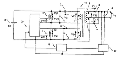
これは、図6に示す従来回路の変圧器22に、変圧器3次巻線6および4次巻線7を付加して変圧器4とし、変圧器3次巻線6をMOSFET2のゲートに抵抗16を介して接続し、変圧器4次巻線7の電圧VP4をダイオード11およびコンデンサ15により半波整流して制御回路18の電源電圧とし、変圧器4次巻線7をその電圧の切替りを検出するために制御回路18に接続した点が特徴である。なお、MOSFET2と並列に接続されるスナバコンデンサは、ここでは図示を省略した。
【0023】
図2に図1のタイミングチャートを示す。以下、その動作について図1も参照して説明する。
【0024】
まず、期間(1)においてMOSFET1は、変圧器4次巻線7の電圧VP4が負から正へ切り替わるタイミングから、短絡防止期間Tdを経たのちにオンする。これにより、コンデンサ3と変圧器4の漏れインダクタンスによる共振電流と変圧器4の励磁電流が、直流電源10→コンデンサ3→変圧器1次巻線5→MOSFET1を介して流れ、コンデンサ3が充電される。このとき、変圧器1次巻線5には直流電源電圧Edとコンデンサ3との差電圧VP1が印加され、変圧器2次巻線8に発生する電圧をダイオード12,コンデンサ14により整流,平滑し負荷に電力を供給する。
【0025】
MOSFET1のオフは、変圧器1次巻線の電圧VP1の負より正に切り替わるタイミングから、制御回路18内において、時間に比例して増加する参照信号値と出力電圧検出回路17からの2次側出力電圧検出値(図2では、出力電圧指令値として示す)とを比較し、参照信号値が出力電圧検出値を上回ったときに行なわれる。また、制御回路18は参照信号値が出力電圧検出値を上回る前に、負荷の状態などにより変圧器4次巻線7の電圧VP4が下降した場合(変圧器3次巻線6の電圧VP3は上昇する)、VP4の正から負に切り替わるタイミングを検出して、MOSFET1をオフさせる。これにより、MOSFET1がオンしている途中で、MOSFET2がオンするといったアーム短絡の発生が防止される。MOSFET1がオフすると、変圧器1次巻線5の電圧VP1は正から負に切り替わる。変圧器3次巻線6と変圧器4次巻線7には、変圧器1次巻線5の巻数比に比例した電圧が発生する。その電圧の極性は変圧器3次巻線6の電圧VP3が正で、変圧器4次巻線7の電圧VP4が負となる。MOSFET1がオフするタイミングでは、ダイオード12に流れる電流は零となっており、MOSFET1がオフする電流は変圧器4の励磁電流のみとなる。
【0026】
期間(2)において、MOSFET1をオフすることにより、変圧器4の励磁電流はMOSFET1,2の出力容量に転流し、MOSFET1,2の電圧は徐々に上昇または下降する。
【0027】
期間(3)において、MOSFET1の電圧が直流電源電圧Edに達すると、変圧器4の励磁電流はMOSFET2の寄生ダイオードに転流する。このとき、変圧器3次巻線6の電圧VP3がMOSFET2のゲートしきい値を越えるとMOSFET2がオンし、コンデンサ3→MOSFET2→変圧器1次巻線5を介して共振電流と変圧器4の励磁電流が流れ、コンデンサ3を放電する。また、変圧器1次巻線5には直流電源電圧Edとコンデンサ3との差電圧VP1が印加され、変圧器2次巻線9に発生する電圧をダイオード13,コンデンサ14により整流,平滑し負荷に電力を供給する。共振電流が下降してくると変圧器3次巻線6の電圧VP3が下降し、それがMOSFET2のゲートしきい値以下になると、MOSFET2はオフする。MOSFET2がオフするタイミングでは、ダイオード13に流れる電流は零となっており、MOSFET2がオフする電流は変圧器4の励磁電流のみとなる。
【0028】
期間(4)においてMOSFET2がオフすると、変圧器1次巻線5の電圧VP1は負から正になる。変圧器3次巻線6と変圧器4次巻線7には、変圧器1次巻線5の巻数比に比例した電圧が発生する。その電圧の極性は変圧器3次巻線6の電圧VP3が負で、変圧器4次巻線7の電圧VP4が正となる。変圧器4の励磁電流はコンデンサ3およびMOSFET1,2の寄生容量に転流し、MOSFET1,2の電圧は徐々に下降または上昇する。期間(1)においてMOSFET2の電圧VQ2が直流電源電圧Edに達すると、変圧器4の励磁電流はMOSFET1の寄生ダイオードに転流する。以後この一連の動作を繰り返すことにより、直流電源10から負荷に電力が供給される。
【0029】
なお、出力電圧検出回路17の出力段は、2次側からの信号を電気的に絶縁するためフォトカプラを用いるのが一般的であるが、フォトカプラの2次側はトランジスタ構造となっているため、出力電圧検出値の最小値はフォトカプラの2次側トランジスタのえん層電圧以下には低下しない。従って、参照電圧信号の最小値が出力電圧検出値の最小値よりも小さい場合、スイッチング周期毎に常にMOSFET1がオンオフするため、軽負荷時や負荷急変時に2次側出力電圧が設定電圧を越えて過電圧になることがある。
【0030】
この問題に対し、ここでは上記参照電圧信号に対しその最小値が、出力電圧検出回路17からの出力の最小値よりも大きくなるようにオフセットを持たせ、さらに出力電圧検出回路17からの出力値が参照電圧信号の最小値よりも小さくなった場合はMOSFET1のオンを抑止し、スイッチングを継続しないようにすることで、2次側出力電圧の過電圧を防ぐようにしている。
【0031】
図3を参照して、この発明によるDC/DCコンバータの誤停止を抑止するための制御回路18の動作につき説明する。
【0032】
期間(1)は負荷急変が発生して出力電圧Voが上昇し、フィードバック制御により電圧指令値が下降した状態(スイッチング停止)を示す。また、回路の動作状態によりコンデンサ3に電荷が残った状態でMOSFET1,2が停止していることを示す。コンデンサ3の電荷は回路中のインピーダンスにより徐々に放電する。期間(2)は、変圧器4次巻線7の電圧切替りが無くなったことを検出して動作する、第1の誤停止抑止回路が動作失敗したときの状態を示す。このとき、コンデンサ3が充分放電していないときには、変圧器1次巻線5に印加される電圧が小さくなり、MOSFET1に駆動信号を与えても変圧器3次巻線6,4次巻線7に発生する電圧も小さくなり、スイッチングが継続できない場合がある。
【0033】
期間(3)では、出力電圧Voが正常値に戻り、電圧指令値が上昇し、さらにコンデンサ3の電荷が充分放電された状態を示す。このとき、或る周波数の矩形波信号の変化(ここでは立ち上がり)のタイミングで、MOSFET1の駆動信号(第2の誤停止抑止信号)を与えることにより、変圧器3次巻線6,4次巻線7に充分電圧が発生し、MOSFET1,2は繰り返しスイッチングを行なうことができる。なお、コンデンサ3の放電を促進するために、コンデンサ3と並列に放電抵抗を接続することができる。
【0034】
図4にこの発明によるDC/DCコンバータの間欠動作を説明するタイムチャートを示す。
【0035】
この間欠動作は、軽負荷の際に意図的にMOSFETのスイッチングを停止させることで、各部で発生する損失を低減し、入力電力を低く抑えるためのものである。間欠動作時においてスイッチング停止期間が短いと、MOSFET1のスイッチングを停止させても、変圧器3次巻線6の電圧変化はすぐには停止しないため、MOSFET2はスイッチングを継続する。スイッチング停止期間が終了しMOSFET1をオンさせるとき、MOSFET2がオンであると直流電源10→MOSFET2→MOSFET1の経路で大電流が流れ(アーム短絡)、回路が破壊するおそれがある。従って、制御回路18により変圧器4次巻線7を監視し、MOSFET2がオフになっている状態のとき(電圧VP4が正電圧または変圧器4次巻線7の電圧の切替わりが停止しているとき)に、再起動信号を出してMOSFET1をオンするようにする。
【0036】
図5はこの発明の第2の実施の形態を示す回路図である。
【0037】
同図からも明らかなように、この例は変圧器24の2次巻線に発生する電圧を半波整流するのにフライバック接続とした点が特徴である。したがって、直流電源10から負荷への電力供給は、MOSFET1がオフになったときのみ行なわれる。なお、その他は図1と同様なので詳細は省略する。
【0038】
【発明の効果】
この発明によれば、入力電圧や負荷の変化に対し、スイッチング周波数の変化に加えてパルス幅制御を行なうようにしたので、軽負荷時に負極に接続したスイッチ素子のオン時間を狭められるため、無効電流による回路中のインピーダンスで発生する損失を低減でき、軽負荷時の効率低下を抑制することができる。また、高電圧(正極)側のスイッチ素子を駆動するに当たり、比較的高価な高耐圧ドライバICまたはパルストランスを不要にできるため、コストの低減と回路の小型化が可能になる、という利点がもたらされる。
【0039】
加えて、2次側出力電圧検出値が参照電圧の最小値よりも下回るようにすることで、2次側出力電圧が設定電圧より大きく上昇しようとした場合には、直流電源の負極側のスイッチ素子をオフ状態として不要なスイッチングを抑止するため、スイッチ素子の発生損失が軽減されるとともに2次側出力電圧の過電圧が防止できる。
【0040】
これに対し、2次側出力電圧検出値が参照電圧を上回ったことを検出したときは、或る一定の周波数で発振する矩形波信号の立上がりまたは立下がりのタイミングで、直流電源の負極側に接続したスイッチ素子に駆動信号を与えることにより、DC/DCコンバータの誤停止を防止できるので、信頼性の高い電源を構築できる。
【図面の簡単な説明】
【図1】 この発明の第1の実施の形態を示す回路図である。
【図2】 図1の動作を説明するためのタイムチャートである。
【図3】 図1のDC/DCコンバータにおける誤停止の防止動作説明図である。
【図4】 図1における間欠動作時のアーム短絡の防止動作説明図である。
【図5】 この発明の第2の実施の形態を示す回路図である。
【図6】 従来例を示す回路図である。
【図7】 図6の動作を説明するためのタイムチャートである。
【図8】 図6における軽負荷時の動作説明図である。
【符号の説明】
1,2…MOSFET(金属酸化物半導体電界効果トランジスタ)、3,14,15…コンデンサ、4,22,24…変圧器、5…変圧器1次巻線、6…変圧器3次巻線、7…変圧器4次巻線、8,9…変圧器2次巻線、10…直流電源、11,12,13…ダイオード、16…抵抗、17…出力電圧検出回路、18…制御回路、19…周波数・位相制御回路、20…高耐圧ドライバIC、21…スナバコンデンサ。[0001]
BACKGROUND OF THE INVENTION
The present invention relates to a DC / DC converter having a half bridge configuration, and more particularly to a control method thereof.
[0002]
[Prior art]
FIG. 6 shows a conventional example.
[0003]
As shown in the figure, a series circuit of a MOSFET (metal oxide semiconductor field effect transistor) 1 and a
[0004]
FIG. 7 shows a timing chart of FIG. The operation will be described below with reference to FIG.
[0005]
First, by turning on the
[0006]
In the period (2) , the transformer primary winding voltage VP1 gradually decreases, and when the voltage proportional to the turns ratio of the transformer primary winding voltage VP1 falls below the output voltage Vo, the
[0007]
In period (3) , when
[0008]
In the period (4) , when the voltage of the
[0009]
Hereinafter, the operations in the periods (4) to (6) are the same as those in the periods (1) to (3), and thus description thereof is omitted.
[0010]
In this way, by repeating a series of operations from the periods (1) to (6) , power is supplied from the
[0011]
Next, the operation at light load will be described with reference to FIG.
[0012]
When the load is light, the frequency /
[0013]
[Problems to be solved by the invention]
In the above conventional example, each MOSFET is alternately switched from a rated load to a no load with a duty of 50%, and an output voltage detection circuit and a frequency / phase control circuit are used to change the load. The output voltage is made constant by adjusting the voltage applied to the next winding and controlling the current supplied to the load.
[0014]
However, in this method, since the value of the exciting current flowing through the exciting inductance of the transformer hardly changes from the rated load to no load, this exciting current becomes a reactive current, and the impedance in the circuit (MOSFET on-resistance, transformer winding) There is a problem that a loss occurs due to a line resistance and the like, and as a result, efficiency at a light load decreases.
[0015]
Further, since the potential of the source terminal of the MOSFET connected to the positive electrode of the DC power supply is different from the potential of the source terminal of the MOSFET connected to the negative electrode of the DC power supply, the signal for driving the MOSFET on the positive electrode side is a pulse transformer or the like. An expensive high voltage driver IC with insulation or a level shift function is required, resulting in an increase in size and cost of the device.
[0016]
Therefore, an object of the present invention is to keep reactive current low and reduce costs by eliminating expensive parts.
[0017]
[Means for Solving the Problems]
In order to solve such a problem, in the invention of
The switch element connected to the negative side of the DC power supply is turned on after a short-circuit prevention period from switching from positive to negative or negative to positive voltage of the transformer quaternary winding, and the switch element is turned on or transformed. When the reference voltage value that increases in proportion to the time from the switching timing of the voltage of the device quaternary winding is compared with the secondary output voltage detection value, and when the reference voltage value exceeds this voltage detection value, A rectangular wave that oscillates at a certain frequency when the DC output voltage is made constant by turning off the switch element and when it is detected that the secondary output voltage detection value exceeds the reference voltage. By supplying a drive signal to the switch element at the rise or fall timing of the signal, erroneous stop of the DC / DC converter is prevented .
In the first aspect of the present invention, a constant offset can be provided so that the minimum value of the reference voltage is larger than the minimum value of the secondary output voltage detection value (the second aspect of the invention). .
[0018]
In the invention of
When the presence or absence of switching from positive to negative or from negative to positive is detected in the voltage of the transformer quaternary winding, the switch element connected to the negative side of the DC power supply is detected. By giving a drive signal, the DC / DC converter is prevented from being erroneously stopped.
[0019]
In the invention of
When it is detected from the voltage of the transformer quaternary winding that the switch element connected to the positive side of the DC power source is turned on while the switch element connected to the negative side of the DC power source is turned on, the DC An arm short circuit is prevented by turning off the switch element connected to the negative side of the power supply.
[0020]
In the invention of
When the load is light, the switching element connected to the negative side of the DC power source is intermittently driven by providing a period for stopping switching and a period for performing switching, and is connected to the negative side of the DC power source. The switching of the switching element from the switching stop period to the switching period is performed when it is detected by the voltage of the transformer quaternary winding that the switching element connected to the positive side of the DC power supply is turned off. It is characterized by preventing a short circuit.
[0021]
DETAILED DESCRIPTION OF THE INVENTION
FIG. 1 is a circuit diagram showing an embodiment of the present invention.
[0022]
This is because the transformer tertiary winding 6 and the quaternary winding 7 are added to the transformer 22 of the conventional circuit shown in FIG. 6 to form the
[0023]
FIG. 2 shows a timing chart of FIG. The operation will be described below with reference to FIG.
[0024]
First, in the period (1) , the
[0025]
The
[0026]
In the period (2) , by turning off the
[0027]
In period (3) , when the voltage of
[0028]
When
[0029]
The output stage of the output
[0030]
In order to solve this problem, the reference voltage signal is offset so that the minimum value of the reference voltage signal is larger than the minimum value of the output from the output
[0031]
Referring to FIG. 3, the operation of
[0032]
Period (1) shows a state (switching stopped) in which a sudden load change occurs, the output voltage Vo increases, and the voltage command value decreases due to feedback control. In addition, it shows that the
[0033]
In the period (3) , the output voltage Vo returns to the normal value, the voltage command value increases, and the charge of the
[0034]
FIG. 4 shows a time chart for explaining the intermittent operation of the DC / DC converter according to the present invention.
[0035]
This intermittent operation is for intentionally stopping the switching of the MOSFET at the time of a light load, thereby reducing the loss generated in each part and keeping the input power low. If the switching stop period is short during intermittent operation, even if switching of the
[0036]
FIG. 5 is a circuit diagram showing a second embodiment of the present invention.
[0037]
As is clear from the figure, this example is characterized in that flyback connection is used for half-wave rectification of the voltage generated in the secondary winding of the
[0038]
【The invention's effect】
According to the present invention, since the pulse width control is performed in addition to the change of the switching frequency with respect to the change of the input voltage and the load, the on-time of the switch element connected to the negative electrode at the time of light load can be narrowed. It is possible to reduce the loss caused by the impedance in the circuit due to the current, and to suppress the efficiency reduction at light load. In addition, when driving the switching element on the high voltage (positive electrode) side, a relatively expensive high-voltage driver IC or pulse transformer can be dispensed with, so that the advantages of cost reduction and circuit miniaturization are brought about. It is.
[0039]
In addition, if the secondary side output voltage is to be increased more than the set voltage by making the secondary side output voltage detection value lower than the minimum value of the reference voltage, the switch on the negative side of the DC power supply Since the element is turned off to suppress unnecessary switching, the generation loss of the switch element is reduced, and overvoltage of the secondary output voltage can be prevented.
[0040]
On the other hand, when it is detected that the detected value of the secondary output voltage exceeds the reference voltage, at the rising or falling timing of the rectangular wave signal oscillating at a certain frequency, By giving a drive signal to the connected switch element, it is possible to prevent erroneous stop of the DC / DC converter, so that a highly reliable power source can be constructed.
[Brief description of the drawings]
FIG. 1 is a circuit diagram showing a first embodiment of the present invention.
FIG. 2 is a time chart for explaining the operation of FIG. 1;
3 is an operation explanatory diagram for preventing erroneous stop in the DC / DC converter of FIG. 1; FIG.
4 is an explanatory diagram of an arm short-circuit prevention operation during intermittent operation in FIG. 1. FIG.
FIG. 5 is a circuit diagram showing a second embodiment of the present invention.
FIG. 6 is a circuit diagram showing a conventional example.
FIG. 7 is a time chart for explaining the operation of FIG. 6;
8 is an operation explanatory diagram at light load in FIG. 6. FIG.
[Explanation of symbols]
DESCRIPTION OF
Claims (5)
前記直流電源の負極側に接続したスイッチ素子は、変圧器4次巻線の電圧の正から負または負から正への切替りから短絡防止期間を経た後にオンとし、前記スイッチ素子のオンまたは変圧器4次巻線の電圧の切替りタイミングから時間に比例して増加する参照電圧値を2次側出力電圧検出値と比較し、この電圧検出値に対して前記参照電圧値が上回ったとき、前記スイッチ素子をオフさせることにより、直流出力電圧を一定とするとともに、前記2次側出力電圧検出値が前記参照電圧を上回ったことを検出したときは、或る一定の周波数で発振する矩形波信号の立ち上がりまたは立ち下がりのタイミングで、前記スイッチ素子に駆動信号を与えることにより、前記DC/DCコンバータの誤停止を防止することを特徴とするDC/DCコンバータの制御方法。A series circuit of two switch elements is connected in parallel between the positive electrode and the negative electrode of the DC power supply, and a series circuit of at least one capacitor and a transformer primary winding is connected in parallel to one of the switch elements, The switch element connected to the positive side of the DC power supply is given an on / off signal from the tertiary winding of the transformer, while the quaternary winding of the transformer is used for the power supply of the control circuit, and 4 The positive / negative voltage generated in the secondary winding of the transformer is detected by detecting the timing of the positive / negative switching of the secondary winding voltage and giving an ON / OFF signal to the switch element connected to the negative side of the DC power supply at that timing. In a DC / DC converter that obtains a direct current output by half-wave or full-wave rectification ,
The switch element connected to the negative side of the DC power supply is turned on after a short-circuit prevention period from switching from positive to negative or negative to positive voltage of the transformer quaternary winding, and the switch element is turned on or transformed. When the reference voltage value that increases in proportion to the time from the switching timing of the voltage of the device quaternary winding is compared with the secondary output voltage detection value, and when the reference voltage value exceeds this voltage detection value, A rectangular wave that oscillates at a certain frequency when the DC output voltage is made constant by turning off the switch element and when it is detected that the secondary output voltage detection value exceeds the reference voltage. at a rising or falling edge of the signal, by applying a drive signal to the switching element, DC / DC converter, characterized in that to prevent erroneous stop of the DC / DC converter Method of controlling the data.
前記変圧器4次巻線の電圧の正から負または負から正への切替りの有無を検出し、切替りの無いことを検出したときは、前記直流電源の負極側に接続したスイッチ素子に駆動信号を与えることにより、前記DC/DCコンバータの誤停止を防止することを特徴とするDC/DCコンバータの制御方法。 A series circuit of two switch elements is connected in parallel between the positive electrode and the negative electrode of the DC power supply, and a series circuit of at least one capacitor and a transformer primary winding is connected in parallel to one of the switch elements, The switch element connected to the positive side of the DC power supply is given an on / off signal from the tertiary winding of the transformer, while the quaternary winding of the transformer is used for the power supply of the control circuit, and 4 The positive / negative voltage generated in the secondary winding of the transformer is detected by detecting the timing of the positive / negative switching of the secondary winding voltage and giving an ON / OFF signal to the switch element connected to the negative side of the DC power supply at that timing. In a DC / DC converter that obtains a direct current output by half-wave or full-wave rectification,
When the presence or absence of switching from positive to negative or from negative to positive is detected in the voltage of the transformer quaternary winding, the switch element connected to the negative side of the DC power supply is detected. A control method for a DC / DC converter , wherein a drive signal is applied to prevent erroneous stop of the DC / DC converter.
前記直流電源の負極側に接続したスイッチ素子がオンしている途中で、直流電源の正極側に接続したスイッチ素子がオンすることを変圧器4次巻線の電圧から検出したときは、前記直流電源の負極側に接続したスイッチ素子をオフすることにより、アーム短絡を防止することを特徴とするDC/DCコンバータの制御方法。 A series circuit of two switch elements is connected in parallel between the positive electrode and the negative electrode of the DC power supply, and a series circuit of at least one capacitor and a transformer primary winding is connected in parallel to one of the switch elements, The switch element connected to the positive side of the DC power supply is given an on / off signal from the tertiary winding of the transformer, while the quaternary winding of the transformer is used for the power supply of the control circuit, and 4 The positive / negative voltage generated in the secondary winding of the transformer is detected by detecting the timing of the positive / negative switching of the secondary winding voltage and giving an ON / OFF signal to the switch element connected to the negative side of the DC power supply at that timing. In a DC / DC converter that obtains a direct current output by half-wave or full-wave rectification,
When it is detected from the voltage of the transformer quaternary winding that the switch element connected to the positive side of the DC power source is turned on while the switch element connected to the negative side of the DC power source is turned on, the DC A control method for a DC / DC converter, wherein an arm short circuit is prevented by turning off a switch element connected to a negative electrode side of a power supply .
負荷が軽いときは、前記直流電源の負極側に接続したスイッチ素子を、スイッチングを停止する期間と、スイッチングを行なう期間とを設けて間欠発振駆動するものであり、直流電源の負極側に接続したスイッチ素子の、スイッチング停止期間からスイッチング期間への切り替えは、変圧器4次巻線の電圧によって、直流電源の正極側に接続したスイッチ素子がオフしていることを検出したときに行なって、アーム短絡を防止することを特徴とするDC/DCコンバータの制御方法。 A series circuit of two switch elements is connected in parallel between the positive electrode and the negative electrode of the DC power supply, and a series circuit of at least one capacitor and a transformer primary winding is connected in parallel to one of the switch elements, The switch element connected to the positive side of the DC power supply is given an on / off signal from the tertiary winding of the transformer, while the quaternary winding of the transformer is used for the power supply of the control circuit, and 4 The positive / negative voltage generated in the secondary winding of the transformer is detected by detecting the timing of the positive / negative switching of the secondary winding voltage and giving an ON / OFF signal to the switch element connected to the negative side of the DC power supply at that timing. In a DC / DC converter that obtains a direct current output by half-wave or full-wave rectification,
When the load is light, the switching element connected to the negative side of the DC power source is intermittently driven by providing a period for stopping switching and a period for performing switching, and is connected to the negative side of the DC power source. The switching of the switching element from the switching stop period to the switching period is performed when it is detected by the voltage of the transformer quaternary winding that the switching element connected to the positive side of the DC power supply is turned off. A method for controlling a DC / DC converter, characterized by preventing a short circuit .
Priority Applications (3)
| Application Number | Priority Date | Filing Date | Title |
|---|---|---|---|
| JP2001074656A JP4423458B2 (en) | 2000-11-10 | 2001-03-15 | Control method of DC / DC converter |
| US09/992,545 US6483722B2 (en) | 2000-11-10 | 2001-11-07 | DC/DC converter and control method thereof |
| DE10154776A DE10154776A1 (en) | 2000-11-10 | 2001-11-08 | DC converter in half bridge configuration for converting DC current to DC current or DC voltage to DC voltage and method for controlling converter |
Applications Claiming Priority (3)
| Application Number | Priority Date | Filing Date | Title |
|---|---|---|---|
| JP2000-342864 | 2000-11-10 | ||
| JP2000342864 | 2000-11-10 | ||
| JP2001074656A JP4423458B2 (en) | 2000-11-10 | 2001-03-15 | Control method of DC / DC converter |
Publications (3)
| Publication Number | Publication Date |
|---|---|
| JP2002209381A JP2002209381A (en) | 2002-07-26 |
| JP2002209381A5 JP2002209381A5 (en) | 2006-05-25 |
| JP4423458B2 true JP4423458B2 (en) | 2010-03-03 |
Family
ID=26603723
Family Applications (1)
| Application Number | Title | Priority Date | Filing Date |
|---|---|---|---|
| JP2001074656A Expired - Fee Related JP4423458B2 (en) | 2000-11-10 | 2001-03-15 | Control method of DC / DC converter |
Country Status (3)
| Country | Link |
|---|---|
| US (1) | US6483722B2 (en) |
| JP (1) | JP4423458B2 (en) |
| DE (1) | DE10154776A1 (en) |
Families Citing this family (26)
| Publication number | Priority date | Publication date | Assignee | Title |
|---|---|---|---|---|
| JP4217950B2 (en) * | 2002-07-26 | 2009-02-04 | 富士電機デバイステクノロジー株式会社 | Control method of DC / DC converter |
| JP4784153B2 (en) * | 2005-05-26 | 2011-10-05 | 富士電機株式会社 | Power supply |
| JP4696725B2 (en) | 2005-06-29 | 2011-06-08 | 富士電機システムズ株式会社 | IC for switching power supply control |
| JP4830408B2 (en) * | 2005-09-01 | 2011-12-07 | 富士電機株式会社 | Power converter |
| US7649474B1 (en) * | 2005-11-16 | 2010-01-19 | The Charles Machine Works, Inc. | System for wireless communication along a drill string |
| JP5040268B2 (en) | 2006-11-10 | 2012-10-03 | 富士電機株式会社 | Switching power supply |
| ES2852223T3 (en) * | 2006-12-20 | 2021-09-13 | Primozone Production Ab | High voltage transformer |
| JP5034568B2 (en) * | 2007-03-09 | 2012-09-26 | 富士電機株式会社 | Switching power supply |
| JP4320787B2 (en) | 2007-05-21 | 2009-08-26 | 株式会社村田製作所 | Switching power supply |
| JP5365136B2 (en) * | 2007-11-01 | 2013-12-11 | 富士電機株式会社 | Power converter drive device |
| EP2421137B1 (en) * | 2009-04-14 | 2019-05-08 | Murata Manufacturing Co., Ltd. | Switching power supply unit |
| EP2421136B1 (en) | 2009-04-14 | 2019-05-08 | Murata Manufacturing Co., Ltd. | Switching power supply unit |
| JP5397534B2 (en) | 2010-02-23 | 2014-01-22 | 株式会社村田製作所 | Switching power supply |
| CN102223075B (en) * | 2011-06-16 | 2013-07-24 | 清华大学 | Four-port direct-current converter |
| JP5937597B2 (en) * | 2011-08-11 | 2016-06-22 | 株式会社村田製作所 | Switching power supply |
| JP5549659B2 (en) | 2011-10-28 | 2014-07-16 | 株式会社村田製作所 | Switching power supply |
| CN104221266B (en) | 2012-03-30 | 2016-11-02 | 株式会社村田制作所 | Switching power unit |
| JP5991078B2 (en) | 2012-08-27 | 2016-09-14 | 富士電機株式会社 | Switching power supply |
| TWI581555B (en) | 2014-09-12 | 2017-05-01 | Alpha And Omega Semiconductor (Cayman) Ltd | Fixed on-time switching converter |
| TWI549412B (en) * | 2014-09-12 | 2016-09-11 | Alpha & Omega Semiconductor Cayman Ltd | Fixed on-time switching type switching device |
| TWI574499B (en) | 2014-09-12 | 2017-03-11 | Alpha And Omega Semiconductor (Cayman) Ltd | Fixed on-time switching type switching device |
| TWI565211B (en) | 2014-09-12 | 2017-01-01 | Alpha And Omega Semiconductor (Cayman) Ltd | Constant on-time switching converter |
| TWI556563B (en) | 2014-09-12 | 2016-11-01 | Alpha & Omega Semiconductor Cayman Ltd | Fixed on-time switching type switching device |
| JP6245385B2 (en) | 2015-01-16 | 2017-12-13 | 富士電機株式会社 | Switching power supply |
| CN109861603B (en) * | 2019-04-17 | 2024-04-23 | 深圳英飞源技术有限公司 | Transformer winding switching method |
| JP2023019535A (en) | 2021-07-29 | 2023-02-09 | スミダコーポレーション株式会社 | Output stabilization circuit and dc/dc converter circuit |
Family Cites Families (3)
| Publication number | Priority date | Publication date | Assignee | Title |
|---|---|---|---|---|
| US4499530A (en) * | 1981-09-30 | 1985-02-12 | Hitachi, Ltd. | Switching power supply apparatus |
| US5438497A (en) * | 1993-05-13 | 1995-08-01 | Northern Telecom Limited | Tertiary side resonant DC/DC converter |
| JP3673075B2 (en) * | 1998-03-09 | 2005-07-20 | 新電元工業株式会社 | Switching power supply |
-
2001
- 2001-03-15 JP JP2001074656A patent/JP4423458B2/en not_active Expired - Fee Related
- 2001-11-07 US US09/992,545 patent/US6483722B2/en not_active Expired - Lifetime
- 2001-11-08 DE DE10154776A patent/DE10154776A1/en not_active Ceased
Also Published As
| Publication number | Publication date |
|---|---|
| US6483722B2 (en) | 2002-11-19 |
| US20020080634A1 (en) | 2002-06-27 |
| JP2002209381A (en) | 2002-07-26 |
| DE10154776A1 (en) | 2002-05-29 |
Similar Documents
| Publication | Publication Date | Title |
|---|---|---|
| JP4423458B2 (en) | Control method of DC / DC converter | |
| US7113380B2 (en) | Power supply device and control method thereof | |
| JP4735072B2 (en) | Switching power supply | |
| US7778048B2 (en) | Switching power supply apparatus | |
| JP3459142B2 (en) | Drive pulse output limiting circuit | |
| US7561449B2 (en) | DC-AC converter and method for protecting DC-AC converter from overcurrent | |
| US7362598B2 (en) | Synchronous rectifier gate drive shutdown circuit | |
| JP3336995B2 (en) | DC-DC converter | |
| US7049793B2 (en) | Boost switching power supply | |
| US7369391B2 (en) | Drive circuit of direct-current voltage-driven magnetic contactor and power converter | |
| JP2001333576A (en) | Method of controlling dc-dc converter | |
| JP3591635B2 (en) | DC-DC converter | |
| JPH11150952A (en) | Switching dc power supply equipment | |
| JP2001145371A (en) | Power supply for sputtering | |
| JP4288702B2 (en) | Switching power supply | |
| US5933333A (en) | Switching power supply apparatus | |
| JP2005045965A (en) | Current resonance type converter device | |
| JP2004215417A (en) | Dc-dc converter | |
| JPH10309078A (en) | Switching dc power unit | |
| JP4395880B2 (en) | Synchronous rectifier circuit for switching power supply | |
| JP4212164B2 (en) | Parallel power supply | |
| JP6717426B2 (en) | Power converter | |
| JPH0767335A (en) | Switching power supply device | |
| JPH114578A (en) | Voltage converter device | |
| JP3373194B2 (en) | Switching power supply |
Legal Events
| Date | Code | Title | Description |
|---|---|---|---|
| A711 | Notification of change in applicant |
Free format text: JAPANESE INTERMEDIATE CODE: A712 Effective date: 20031106 |
|
| RD03 | Notification of appointment of power of attorney |
Free format text: JAPANESE INTERMEDIATE CODE: A7423 Effective date: 20040122 |
|
| RD04 | Notification of resignation of power of attorney |
Free format text: JAPANESE INTERMEDIATE CODE: A7424 Effective date: 20040205 |
|
| A521 | Request for written amendment filed |
Free format text: JAPANESE INTERMEDIATE CODE: A821 Effective date: 20050328 |
|
| A711 | Notification of change in applicant |
Free format text: JAPANESE INTERMEDIATE CODE: A711 Effective date: 20050802 |
|
| A521 | Request for written amendment filed |
Free format text: JAPANESE INTERMEDIATE CODE: A821 Effective date: 20050802 |
|
| A521 | Request for written amendment filed |
Free format text: JAPANESE INTERMEDIATE CODE: A523 Effective date: 20060316 |
|
| A621 | Written request for application examination |
Free format text: JAPANESE INTERMEDIATE CODE: A621 Effective date: 20060316 |
|
| A521 | Request for written amendment filed |
Free format text: JAPANESE INTERMEDIATE CODE: A523 Effective date: 20060405 |
|
| A621 | Written request for application examination |
Free format text: JAPANESE INTERMEDIATE CODE: A621 Effective date: 20060405 |
|
| RD03 | Notification of appointment of power of attorney |
Free format text: JAPANESE INTERMEDIATE CODE: A7423 Effective date: 20060405 |
|
| A977 | Report on retrieval |
Free format text: JAPANESE INTERMEDIATE CODE: A971007 Effective date: 20090227 |
|
| A131 | Notification of reasons for refusal |
Free format text: JAPANESE INTERMEDIATE CODE: A131 Effective date: 20090319 |
|
| A521 | Request for written amendment filed |
Free format text: JAPANESE INTERMEDIATE CODE: A523 Effective date: 20090508 |
|
| A521 | Request for written amendment filed |
Free format text: JAPANESE INTERMEDIATE CODE: A523 Effective date: 20090508 |
|
| TRDD | Decision of grant or rejection written | ||
| A01 | Written decision to grant a patent or to grant a registration (utility model) |
Free format text: JAPANESE INTERMEDIATE CODE: A01 Effective date: 20091020 |
|
| A01 | Written decision to grant a patent or to grant a registration (utility model) |
Free format text: JAPANESE INTERMEDIATE CODE: A01 |
|
| A711 | Notification of change in applicant |
Free format text: JAPANESE INTERMEDIATE CODE: A712 Effective date: 20091112 |
|
| RD03 | Notification of appointment of power of attorney |
Free format text: JAPANESE INTERMEDIATE CODE: A7423 Effective date: 20091112 |
|
| RD04 | Notification of resignation of power of attorney |
Free format text: JAPANESE INTERMEDIATE CODE: A7424 Effective date: 20091112 |
|
| A61 | First payment of annual fees (during grant procedure) |
Free format text: JAPANESE INTERMEDIATE CODE: A61 Effective date: 20091119 |
|
| R150 | Certificate of patent or registration of utility model |
Free format text: JAPANESE INTERMEDIATE CODE: R150 |
|
| FPAY | Renewal fee payment (event date is renewal date of database) |
Free format text: PAYMENT UNTIL: 20121218 Year of fee payment: 3 |
|
| FPAY | Renewal fee payment (event date is renewal date of database) |
Free format text: PAYMENT UNTIL: 20121218 Year of fee payment: 3 |
|
| S111 | Request for change of ownership or part of ownership |
Free format text: JAPANESE INTERMEDIATE CODE: R313111 |
|
| FPAY | Renewal fee payment (event date is renewal date of database) |
Free format text: PAYMENT UNTIL: 20121218 Year of fee payment: 3 |
|
| R350 | Written notification of registration of transfer |
Free format text: JAPANESE INTERMEDIATE CODE: R350 |
|
| FPAY | Renewal fee payment (event date is renewal date of database) |
Free format text: PAYMENT UNTIL: 20121218 Year of fee payment: 3 |
|
| FPAY | Renewal fee payment (event date is renewal date of database) |
Free format text: PAYMENT UNTIL: 20131218 Year of fee payment: 4 |
|
| R250 | Receipt of annual fees |
Free format text: JAPANESE INTERMEDIATE CODE: R250 |
|
| R250 | Receipt of annual fees |
Free format text: JAPANESE INTERMEDIATE CODE: R250 |
|
| R250 | Receipt of annual fees |
Free format text: JAPANESE INTERMEDIATE CODE: R250 |
|
| LAPS | Cancellation because of no payment of annual fees |