JP4423402B2 - Redundant transmission device - Google Patents
Redundant transmission device Download PDFInfo
- Publication number
- JP4423402B2 JP4423402B2 JP2000223568A JP2000223568A JP4423402B2 JP 4423402 B2 JP4423402 B2 JP 4423402B2 JP 2000223568 A JP2000223568 A JP 2000223568A JP 2000223568 A JP2000223568 A JP 2000223568A JP 4423402 B2 JP4423402 B2 JP 4423402B2
- Authority
- JP
- Japan
- Prior art keywords
- unit
- switching
- control
- standby
- basic
- Prior art date
- Legal status (The legal status is an assumption and is not a legal conclusion. Google has not performed a legal analysis and makes no representation as to the accuracy of the status listed.)
- Expired - Lifetime
Links
- 230000005540 biological transmission Effects 0.000 title claims description 46
- 238000004891 communication Methods 0.000 claims description 34
- 238000010586 diagram Methods 0.000 description 6
- 238000010187 selection method Methods 0.000 description 4
- 239000000284 extract Substances 0.000 description 3
- 230000005856 abnormality Effects 0.000 description 2
- 238000013507 mapping Methods 0.000 description 2
- 238000000034 method Methods 0.000 description 2
- 238000001514 detection method Methods 0.000 description 1
- 230000000694 effects Effects 0.000 description 1
Images

Landscapes
- Synchronisation In Digital Transmission Systems (AREA)
- Detection And Prevention Of Errors In Transmission (AREA)
- Monitoring And Testing Of Exchanges (AREA)
- Maintenance And Management Of Digital Transmission (AREA)
Description
【0001】
【発明の属する技術分野】
本発明は、冗長構成を有する伝送装置に関し、特に、現用・予備の切替を行う伝送装置に関する。
【0002】
【従来の技術】
一般に伝送装置は、1の基本ユニットと、この基本ユニットに接続される1又は複数の増設ユニットによって構成される。増設ユニットは、収容回線数の増加に応じて随時増設可能なものであり、基本ユニットと各増設ユニットとの間は、それぞれ異なる信号線で接続され、相互にユニット間通信フレームの送受信ができるようになっている。
【0003】
図4に従来の伝送装置におけるユニット間接続の一例を示す。同図に示すように、基本ユニット102は、現用系としての0系インターフェース(I/F)部104、待機系としての1系インターフェース(I/F)部106を備えている。同様に増設ユニット112は、現用系としての0系インターフェース(I/F)部114、待機系としての1系インターフェース(I/F)部116を備えている。
【0004】
各I/F部の送端側は、接続相手のユニットの各I/F部の受端側のそれぞれと信号線により接続されている。すなわち、各I/F部の受端側は、接続相手のユニットの各I/F部の送端側のそれぞれと接続されており、セレクタによる切替動作で何れかのI/F部の送端側を選択するようになっている。この選択方式は、マルチ出力受端選択方式と呼ばれるものである。
【0005】
例えば、通常運用時においては、0系I/F部104と0系I/F部114が動作し、0系I/F部104の送端側から送出されたユニット間通信フレームは0系I/F部114の受端側で受信され、0系I/F部114の送端側から送出されたユニット間通信フレームは0系I/F部104の受端側で受信される。しかし、増設ユニット112内の0系I/F部114に異常が生じた場合には、ソフトウェア制御により、基本ユニット102内の0系I/F部104の受端側のセレクタ105が切り替えられ、増設ユニット112内の1系I/F部116の送端側と接続されるとともに、増設ユニット112内の1系I/F部116の受端側のセレクタ117が切り替えられ、基本ユニット102内の0系I/F部104の送端側と接続される。以上の切替動作により、0系I/F部104と1系I/F部116との間でフレーム伝送が行われることになる。
【0006】
【発明が解決しようとする課題】
しかしながら、上述したようにマルチ出力受端選択方式を採用すると、ユニット間を接続する信号線の本数が多くなるため、高密度実装が要求される現在では、必ずしも適切な方式ではない。また、上述したような切替動作を行う際には、各ユニットの制御部(CPU)同士がファームウェア(F/W)通信処理により、複数のセレクタに対して制御を行うため、切替完了までに時間を要することがあった。このため、高密度実装が可能で且つ障害時におけるI/F部の切替動作を迅速に行うことが可能な冗長構成を有する伝送装置が要求されていた。
【0007】
本発明は、上記従来の問題点を解決するものであり、その目的は高密度実装が可能で且つ障害時におけるI/F部の切替動作を迅速に行うことが可能な冗長構成を有する伝送装置を提供することにある。
【0008】
【課題を解決するための手段】
上記目的を達成するため、本発明の冗長構成を有する伝送装置は、現用系及び待機系として使用される一対のインターフェース部を備えた第1のユニットと、現用系及び待機系として使用される一対のインターフェース部を備え、前記第1のユニットとデータ通信を行う第2のユニットと、前記第1及び第2のユニットの各インターフェース部の現用系と待機系の切替を制御する制御部とを有するものであり、前記第1及び第2のユニットの各インターフェース部は、それが待機系である場合に、前記制御部から送られる現用系への切替要求に応じて、それと対をなす現用系の前記インターフェース部に待機系への切替要求を送信する切替要求送信部、及び他のユニットの待機系のインターフェース部に対し、現用系と待機系の切替要求を設定したユニット間通信フレームを送信するフレーム送信部と、それが現用系である場合に、前記待機系への切替要求を受信する切替要求受信部と、現用系と待機系の切替を所定のタイミングで行う切替制御部とを備える。
【0009】
この場合において、所定のクロックパルスを生成するクロックパルス生成手段を更に備え、前記各切替制御部は、前記生成されたクロックパルスに基づいて、現用系と待機系の切替タイミングの同期を取ることが好ましい。
【0010】
また、前記フレーム送信部は、更に前記現用系と待機系の切替要求のビット列を反転したビット列を設定した前記ユニット間通信フレームを送信することが好ましい。
【0011】
また、前記フレーム送信部は、更に所定のフレーム同期パターン設定した前記ユニット間通信フレームを送信することが好ましい。
【0012】
【発明の実施の形態】
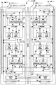
以下、図示した一実施形態に基づいて本発明を詳細に説明する。図1は、本発明に係る伝送装置の構成例を示すブロック図である。同図に示す伝送装置2は、基本ユニット4、増設ユニット6を備えており、これら基本ユニット4と増設ユニット6との間で、ユニット間通信フレームのやりとりが行われる。
【0013】
基本ユニット4は、制御部12、基本ユニット1系インターフェース(I/F)部14、基本ユニット0系インターフェース(I/F)部16、クロック生成部18を備えて構成されている。一方、増設ユニット6は、制御部22、増設ユニット1系インターフェース(I/F)部24、増設ユニット0系インターフェース(I/F)部26、クロック生成部28を備えて構成されている。
【0014】
基本ユニット4と増設ユニット6の間は、基本ユニット0系I/F部16と増設ユニット0系I/F部26が、基本ユニット4から増設ユニット6へ向かうデータを伝送する信号線(下り回線)32及び増設ユニット6から基本ユニット4へ向かうデータを伝送する信号線(上り回線)34によって接続され、基本ユニット1系I/F部14と増設ユニット0系I/F部24が、基本ユニット4から増設ユニット6へ向かうデータを伝送する信号線(下り回線)36及び増設ユニット6から基本ユニット4へ向かうデータを伝送する信号線(上り回線)38によって接続されている。
【0015】
なお、以下においては、基本ユニット0系I/F部16及び増設ユニット0系I/F部26が現用系、基本ユニット1系I/F部14及び増設ユニット1系I/F部24が待機系となっており、現用系である基本ユニット0系I/F部16及び増設ユニット0系I/F部26の間で、ユニット間通信フレームのやりとりが行われているときに、系切替が発生する場合について説明する。
【0016】
基本ユニット4の制御部12は、基本ユニット4及び増設ユニット6内の各I/F部の系切替を制御するものである。具体的には、制御部12は、外部からの制御又は装置内の異常検出(例えば基本ユニット0系I/F部16の障害発生)により、系切替の必要が生じた場合には、待機系である基本ユニット1系I/F部14に対し、待機系から現用系に切り替える要求を送出する。
【0017】
基本ユニット1系I/F部14は、ハードウェア(H/W)制御部40、ペア系制御送信部42、ペア系制御受信部44、基本ユニット制御送信部46、基本ユニット状態受信部48、スイッチ部49を備えている。
【0018】
H/W制御部40は、制御部12からの系切替要求を受信すると、現用系である基本ユニット0系I/F部16に対し、現用系から待機系に切り替える要求を送出する。この系切替要求は、ペア系制御送信部42及びバックワイヤードボード(BWB)バス20を介して基本ユニット0系I/F部16へ送られる。
【0019】
また、H/W制御部40は、基本ユニット0系I/F部16への系切替要求の送出と並行して、ユニット間通信フレームの所定位置のタイムスロットに系の切替要求、該系の切替要求のビット列を反転したビット列(以下、「切替要求反転ビット」と称する)及びフレーム同期パターンを設定する。
【0020】
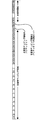
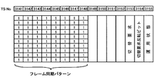
図2は、ユニット間通信フレームの一例を示す図である。同図に示すユニット間通信フレームは、10ビットのビット長を有するタイムスロットを3156個分結合して構成される。このうち、1番目から3016番目までのタイムスロットには、主信号のマッピング領域として用いられている。また、3017番目のタイムスロットには、主信号マッピング領域のパリティビットがマッピングされ、3018番目のタイムスロットには、該パリティビットの反転ビットがマッピングされる。
【0021】
このため、3019番目以降のタイムスロットが未使用になっており、図3に示すように、これら未使用のタイムスロットのうち、3141番目から3148番目のタイムスロットにフレーム同期パターンが設定される。また、3153番目のタイムスロットに系の切替要求が設定され、3154番目のタイムスロットに切替要求反転ビットが設定される。なお、3155番目のタイムスロットには、運用状態が設定されるが、この運用状態の設定方法については後述する。
【0022】
H/W制御部40は、このようにして系の切替要求、切替要求反転ビット及びフレーム同期パターンを設定したユニット間通信フレームを、基本ユニット制御送信部46及び下り回線36を介して、増設ユニット6の待機系である増設ユニット1系I/F部24へ送出する。
【0023】
上述した基本ユニット0系I/F部16に対する系の切替要求の送出と、増設ユニット1系I/F部24に対するユニット間通信フレームの送出の後、H/W制御部40は、所定のタイミングでスイッチ49をオフ状態からオン状態にする。これにより、基本ユニット1系I/F部14は、待機系から現用系に切り替わることになる。
【0024】
基本ユニット0系I/F部16は、ハードウェア(H/W)制御部50、ペア系制御送信部52、ペア系制御受信部54、基本ユニット制御送信部56、基本ユニット状態受信部58、スイッチ部59を備えている。
【0025】
ペア系制御受信部54は、基本ユニット1系I/F部14からの系の切替要求を受信し、H/W制御部50へ送出する。H/W制御部50は、この系の切替要求を受信すると、所定のタイミングでスイッチ59をオン状態からオフ状態にする。これにより、基本ユニット0系I/F部16は、現用系から待機系に切り替わることになる。
【0026】
増設ユニット1系I/F部24は、ハードウェア(H/W)制御部60、ペア系制御送信部62、ペア系制御受信部64、増設ユニット状態送信部66、増設ユニット制御受信部68、スイッチ部69を備えている。
【0027】
増設ユニット制御受信部68は、基本ユニット1系I/F部14からのユニット間通信フレームを受信し、H/W制御部60へ送出する。H/W制御部60は、このユニット間通信フレーム内のフレーム同期パターンを検出する。図3に示したように、ユニット間通信フレームには、フレーム同期パターンの4タイムスロット後に系の切替要求と切替要求反転ビットが設定されている。このため、H/W制御部60は、フレーム同期パターンを検出した場合には、その4タイムスロット後に系の切替要求と切替要求反転ビットが設定されていると判断し、これら系の切替要求と切替要求反転ビットを抽出する。
【0028】
系の切替要求と切替要求反転ビットの抽出後、H/W制御部60は、切替要求反転ビットが系の切替要求のビット列を反転したものになっているか否かを判定する。このような判定を行うことにより、系の切替要求の信頼性を判断することができる。すなわち、切替要求反転ビットが系の切替要求のビット列を反転したものになっていれば、系の切替要求にビット誤りが生じている可能性は極めて小さく、該系の切替要求の信頼性は高いといえる。一方、切替要求反転ビットが系の切替要求のビット列を反転したものになっていなければ、系の切替要求ににビット誤りが生じている可能性は大きく、該系の切替要求の信頼性は低いといえる。
【0029】
系の切替要求の信頼性を判定した後、H/W制御部60は、現用系である増設ユニット0系I/F部26に対し、現用系から待機系に切り替える要求を送出する。この系切替要求は、ペア系制御送信部62及びバックワイヤードボード(BWB)バス30を介して増設ユニット0系I/F部26へ送られる。
【0030】
上述した増設ユニット0系I/F部26に対する系の切替要求の送出の後、H/W制御部60は、所定のタイミングでスイッチ69をオフ状態からオン状態にする。これにより、増設ユニット1系I/F部24は、待機系から現用系に切り替わることになる。
【0031】
なお、受信したユニット間通信フレーム内の系の切替要求の信頼性が低い場合には、上述した増設ユニット0系I/F部26に対する系の切替要求の送出や、スイッチ69の切替は行わなくてもよい。
【0032】
増設ユニット0系I/F部26は、ハードウェア(H/W)制御部70、ペア系制御送信部72、ペア系制御受信部74、増設ユニット状態送信部76、増設ユニット制御受信部78、スイッチ部79を備えている。
【0033】
ペア系制御受信部74は、増設ユニット1系I/F部24からの系の切替要求を受信し、H/W制御部70へ送出する。H/W制御部70は、この系の切替要求を受信すると、所定のタイミングでスイッチ69をオン状態からオフ状態にする。これにより、増設ユニット0系I/F部26は、現用系から待機系に切り替わることになる。
【0034】
基本ユニット4のクロック生成部18は、上述した各I/F部内のH/W制御部によるスイッチの切替タイミングの同期を取るためのクロックパルスを生成するものであり、生成したクロックパルスを基本ユニット1系I/F部14のH/W制御部40と基本ユニット0系I/F部16のH/W制御部50とに供給するとともに、増設ユニット6のクロック生成部28に供給する。クロック生成部28は供給されたクロックパルスを増設ユニット1系I/F部24のH/W制御部60と増設ユニット0系I/F部26のH/W制御部70とに供給する。
【0035】
各I/F部のH/W制御部は、供給されるクロックパルスに基づいて、同時にスイッチを切り替える。これにより、各I/F部の系切替のタイミングを一致させることができる。
【0036】
以上のように、各I/F部のH/W制御部がスイッチを切り替えることにより、系の切替が終了すると、基本ユニット1系I/F部14と増設ユニット1系I/F部24が現用系、基本ユニット0系I/F部16と増設ユニット0系I/F部26が待機系となり、基本ユニット4のBWBバス20と増設ユニット6のBWBバス30が基本ユニット1系I/F部14、下り回線36、上り回線38及び増設ユニット1系I/F部24によって接続され、これらを介してユニット間通信フレームがやりとりされることになる。
【0037】
系切替の終了後、増設ユニット1系I/F部24内のH/W制御部60は、ユニット間通信フレームの所定位置のタイムスロット(図4に示した3155番目のタイムスロット)に、増設ユニット1系I/F部24の運用状態(現用系)を設定し、増設ユニット状態送信部66及び上り回線38を介して、基本ユニット1系I/F部14へ送出する。
【0038】
基本ユニット1系I/F部14の基本ユニット状態受信部48は、このユニット間通信フレームを受信し、H/W制御部40に送出する。H/W制御部40は、受信したユニット間通信フレームから増設ユニット1系I/F部24の運用状態を抽出し、基本ユニット1系I/F部14の運用状態(現用系)とともに、制御部12へ送出する。
【0039】
同様に、増設ユニット0系I/F部26内のH/W制御部70は、ユニット間通信フレームの所定位置のタイムスロット(図3に示した3155番目のタイムスロット)に、増設ユニット0系I/F部26の運用状態(待機系)を設定し、増設ユニット状態送信部76及び上り回線34を介して、基本ユニット0系I/F部16へ送出する。
【0040】
基本ユニット0系I/F部16の基本ユニット状態受信部58は、このユニット間通信フレームを受信し、H/W制御部50に送出する。H/W制御部50は、受信したユニット間通信フレームから増設ユニット0系I/F部26の運用状態を抽出し、基本ユニット0系I/F部16の運用状態(待機系)とともに、制御部12へ送出する。
【0041】
制御部12は、これらの運用状態を受信することにより、各I/F部の運用状態を認識し、系切替が終了したか否かを判断することが可能となる。
【0042】
このように、伝送装置2のI/F部間の接続状態は、基本ユニット0系I/F部16が下り回線32及び上り回線34を介して増設ユニット0系I/F部26のみと接続され、基本ユニット1系I/F部14が下り回線36及び上り回線38を介して増設ユニット1系I/F部24のみと接続されている。このため、マルチ出力受端選択方式と比較すると、接続する信号線の本数が少なくなり、高密度実装に適したものとなる。また、伝送装置2では、系の切替制御をハードウェア処理により行うため、切替完了までに時間を要することがない。
【0043】
以上、本発明の一実施形態を図面に沿って説明した。しかしながら本発明は前記実施形態に示した事項に限定されず、特許請求の範囲の記載に基いてその変更、改良等が可能であることは明らかである。
【0044】
例えば上述した実施形態では、基本ユニット0系I/F部16及び増設ユニット0系I/F部26が現用系、基本ユニット1系I/F部14及び増設ユニット1系I/F部24が待機系となっており、現用系である基本ユニット0系I/F部16及び増設ユニット0系I/F部26の間で、ユニット間通信フレームのやりとりが行われているときに、系切替が発生する場合について説明したが、基本ユニット1系I/F部14及び増設ユニット1系I/F部24が現用系、基本ユニット0系I/F部16及び増設ユニット0系I/F部26が待機系となっており、現用系である基本ユニット1系I/F部14及び増設ユニット1系I/F部24の間で、ユニット間通信フレームのやりとりが行われているときに、系切替が発生する場合についても同様に本発明を適用することができる。
【0045】
【発明の効果】
以上の如く本発明によれば、高密度実装が可能で且つ障害時におけるI/F部の切替動作を迅速に行うことが可能となる。
【図面の簡単な説明】
【図1】本発明に係る伝送装置の構成例を示すブロック図である。
【図2】ユニット間通信フレームの一例を示す図である。
【図3】ユニット間通信フレームにおける、系の切替要求、切替要求反転ビット、フレーム同期パターン及び運用状態の設定位置の一例を示す図である。
【図4】従来の伝送装置におけるユニット間接続の一例を示す図である。
【符号の説明】
2 伝送装置
4 基本ユニット
6 増設ユニット
12 制御部
14 基本ユニット1系I/F部
16 基本ユニット0系I/F部
18 クロック生成部
20 BWBバス
22 制御部
24 増設ユニット1系I/F部
26 増設ユニット0系I/F部
28 クロック生成部
30 BWBバス
32 下り回線
34 上り回線
36 下り回線
38 上り回線
40 H/W制御部
42 ペア系制御送信部
44 ペア系制御受信部
46 基本ユニット制御送信部
48 基本ユニット状態受信部
49 スイッチ部
50 H/W制御部
52 ペア系制御送信部
54 ペア系制御受信部
56 基本ユニット制御送信部
58 基本ユニット状態受信部
59 スイッチ部
60 H/W制御部
62 ペア系制御送信部
64 ペア系制御受信部
66 増設ユニット状態送信部
68 増設ユニット制御受信部
69 スイッチ部
70 H/W制御部
72 ペア系制御送信部
74 ペア系制御受信部
76 増設ユニット状態送信部
78 増設ユニット制御受信部
79 スイッチ部[0001]
BACKGROUND OF THE INVENTION
The present invention relates to a transmission apparatus having a redundant configuration, and more particularly to a transmission apparatus that switches between active and standby.
[0002]
[Prior art]
In general, a transmission apparatus includes one basic unit and one or a plurality of extension units connected to the basic unit. The expansion unit can be expanded at any time according to the increase in the number of accommodated lines, and the basic unit and each expansion unit are connected by different signal lines so that they can transmit and receive inter-unit communication frames. It has become.
[0003]
FIG. 4 shows an example of inter-unit connection in a conventional transmission apparatus. As shown in the figure, the basic unit 102 includes a 0-system interface (I / F) section 104 as an active system and a 1-system interface (I / F) section 106 as a standby system. Similarly, the extension unit 112 includes a 0-system interface (I / F) unit 114 as an active system and a 1-system interface (I / F) unit 116 as a standby system.
[0004]
The sending end side of each I / F unit is connected to each receiving end side of each I / F unit of the connection partner unit by a signal line. That is, the receiving end side of each I / F unit is connected to the sending end side of each I / F unit of the connection partner unit, and the sending end of any I / F unit is switched by the selector operation. The side is to be selected. This selection method is called a multi-output receiving end selection method.
[0005]
For example, during normal operation, the 0-system I / F unit 104 and the 0-system I / F unit 114 operate, and the inter-unit communication frame sent from the sending end side of the 0-system I / F unit 104 is 0-system I. The inter-unit communication frame received at the receiving end of the / F unit 114 and sent from the transmitting end of the 0-system I / F unit 114 is received at the receiving end of the 0-system I / F unit 104. However, when an abnormality occurs in the 0-system I / F unit 114 in the extension unit 112, the
[0006]
[Problems to be solved by the invention]
However, when the multi-output receiving end selection method is adopted as described above, the number of signal lines connecting between the units increases, so that it is not always an appropriate method at present when high-density mounting is required. Further, when the switching operation as described above is performed, the control units (CPUs) of the units control the plurality of selectors by firmware (F / W) communication processing. Sometimes required. For this reason, there has been a demand for a transmission apparatus having a redundant configuration capable of high-density mounting and capable of promptly switching the I / F unit at the time of failure.
[0007]
The present invention solves the above-described conventional problems, and an object of the present invention is to provide a transmission apparatus having a redundant configuration capable of high-density mounting and capable of quickly switching the I / F unit in the event of a failure. Is to provide.
[0008]
[Means for Solving the Problems]
In order to achieve the above object, a transmission apparatus having a redundant configuration according to the present invention includes a first unit including a pair of interface units used as an active system and a standby system, and a pair used as an active system and a standby system. A second unit that performs data communication with the first unit, and a control unit that controls switching between the active system and the standby system of each interface unit of the first and second units. Each of the interface units of the first and second units, when it is a standby system, responds to a switch request to the active system sent from the control unit, A switching request transmission unit that transmits a switching request to the standby system to the interface unit and a standby system interface unit of another unit are provided with a switching request between the active system and the standby system. A frame transmission unit that transmits the inter-unit communication frame, a switching request receiving unit that receives a request to switch to the standby system when it is the active system, and switching between the active system and the standby system at a predetermined timing. A switching control unit to perform.
[0009]
In this case, it further comprises clock pulse generation means for generating a predetermined clock pulse, and each of the switching control units can synchronize the switching timing of the active system and the standby system based on the generated clock pulse. preferable.
[0010]
Further, it is preferable that the frame transmission unit further transmits the inter-unit communication frame in which a bit string obtained by inverting the bit string of the switching request between the active system and the standby system is set.
[0011]
Further, it is preferable that the frame transmission unit further transmits the inter-unit communication frame set with a predetermined frame synchronization pattern.
[0012]
DETAILED DESCRIPTION OF THE INVENTION
Hereinafter, the present invention will be described in detail based on the illustrated embodiment. FIG. 1 is a block diagram illustrating a configuration example of a transmission apparatus according to the present invention. The transmission apparatus 2 shown in the figure includes a
[0013]
The
[0014]
Between the
[0015]
In the following, the basic unit 0 system I / F unit 16 and the extension unit 0 system I / F unit 26 are active, and the
[0016]
The
[0017]
The
[0018]
When receiving the system switching request from the
[0019]
In parallel with the transmission of the system switching request to the basic unit 0 system I / F unit 16, the H /
[0020]
FIG. 2 is a diagram illustrating an example of an inter-unit communication frame. The inter-unit communication frame shown in the figure is configured by combining 3156 time slots having a bit length of 10 bits. Of these, the first to 3016th time slots are used as the main signal mapping area. The parity bit of the main signal mapping area is mapped to the 3017th time slot, and the inverted bit of the parity bit is mapped to the 3018th time slot.
[0021]
For this reason, the 3019th and subsequent time slots are unused, and as shown in FIG. 3, frame synchronization patterns are set in the 3141st to 3148th time slots among these unused time slots. Further, a system switching request is set in the 3153rd time slot, and a switching request inversion bit is set in the 3154th time slot. The operation state is set in the 3155th time slot. A method for setting the operation state will be described later.
[0022]
The H /
[0023]
After sending the system switching request to the basic unit 0 system I / F unit 16 and sending the inter-unit communication frame to the
[0024]
The basic unit 0 system I / F unit 16 includes a hardware (H / W)
[0025]
The pair system
[0026]
The
[0027]
The extension unit
[0028]
After extracting the system switching request and the switching request inversion bit, the H /
[0029]
After determining the reliability of the system switching request, the H /
[0030]
After sending the system switching request to the extension unit 0 system I / F unit 26 described above, the H /
[0031]
If the reliability of the system switching request in the received inter-unit communication frame is low, the system switching request is not sent to the extension unit 0 system I / F unit 26 or the
[0032]
The expansion unit 0 system I / F unit 26 includes a hardware (H / W) control unit 70, a pair system
[0033]
The pair system
[0034]
The
[0035]
The H / W control unit of each I / F unit switches the switches simultaneously based on the supplied clock pulse. Thereby, the system switching timing of each I / F unit can be matched.
[0036]
As described above, when the system switching is completed by switching the switch by the H / W control unit of each I / F unit, the
[0037]
After the system switching is completed, the H /
[0038]
The basic unit
[0039]
Similarly, the H / W control unit 70 in the extension unit 0 system I / F unit 26 sets the extension unit 0 system in the time slot (the 3155th time slot shown in FIG. 3) at a predetermined position of the inter-unit communication frame. The operating state (standby system) of the I / F unit 26 is set, and is transmitted to the basic unit 0 system I / F unit 16 via the extension unit
[0040]
The basic unit
[0041]
By receiving these operation states, the
[0042]
As described above, the connection state between the I / F units of the transmission apparatus 2 is such that the basic unit 0 system I / F unit 16 is connected only to the extension unit 0 system I / F unit 26 via the
[0043]
The embodiment of the present invention has been described with reference to the drawings. However, the present invention is not limited to the matters shown in the above-described embodiments, and it is obvious that changes, improvements, etc. can be made based on the description of the scope of claims.
[0044]
For example, in the embodiment described above, the basic unit 0 system I / F unit 16 and the expansion unit 0 system I / F unit 26 are the active system, and the
[0045]
【The invention's effect】
As described above, according to the present invention, high-density mounting is possible, and the switching operation of the I / F unit at the time of failure can be performed quickly.
[Brief description of the drawings]
FIG. 1 is a block diagram illustrating a configuration example of a transmission apparatus according to the present invention.
FIG. 2 is a diagram illustrating an example of an inter-unit communication frame.
FIG. 3 is a diagram illustrating an example of a setting position of a system switching request, a switching request inversion bit, a frame synchronization pattern, and an operation state in an inter-unit communication frame.
FIG. 4 is a diagram illustrating an example of inter-unit connection in a conventional transmission apparatus.
[Explanation of symbols]
2
Claims (4)
前記第1及び第2のユニットの各インターフェース部は、
それが待機系である場合に、前記制御部から送られる現用系への切替要求に応じて、それと対をなす現用系の前記インターフェース部に待機系への切替要求を送信する切替要求送信部、及び他のユニットの待機系のインターフェース部に対し、現用系と待機系の切替要求を設定したユニット間通信フレームを送信するフレーム送信部と、
それが現用系である場合に、前記待機系への切替要求を受信する切替要求受信部と、
現用系と待機系の切替を所定のタイミングで行う切替制御部と、
を備えることを特徴とする冗長構成を有する伝送装置。A first unit having a pair of interface units used as an active system and a standby system, and a second unit having a pair of interface units used as an active system and a standby system and performing data communication with the first unit And a control unit that controls switching between the active system and the standby system of each interface unit of the first and second units,
Each interface unit of the first and second units is
When it is a standby system, in response to a switch request to the active system sent from the control unit, a switch request transmission unit that transmits a switch request to the standby system to the interface unit of the active system paired with it, And a frame transmission unit that transmits an inter-unit communication frame in which a request for switching between the active system and the standby system is set to the standby interface unit of another unit,
A switching request receiving unit for receiving a switching request to the standby system when it is the active system;
A switching control unit for switching between the active system and the standby system at a predetermined timing;
A transmission apparatus having a redundant configuration.
前記各切替制御部は、前記生成されたクロックパルスに基づいて、現用系と待機系の切替タイミングの同期を取ることを特徴とする請求項1に記載の冗長構成を有する伝送装置。A clock pulse generating means for generating a predetermined clock pulse;
2. The transmission apparatus having a redundant configuration according to claim 1, wherein each switching control unit synchronizes switching timing between an active system and a standby system based on the generated clock pulse.
Priority Applications (1)
| Application Number | Priority Date | Filing Date | Title |
|---|---|---|---|
| JP2000223568A JP4423402B2 (en) | 2000-07-25 | 2000-07-25 | Redundant transmission device |
Applications Claiming Priority (1)
| Application Number | Priority Date | Filing Date | Title |
|---|---|---|---|
| JP2000223568A JP4423402B2 (en) | 2000-07-25 | 2000-07-25 | Redundant transmission device |
Publications (2)
| Publication Number | Publication Date |
|---|---|
| JP2002044058A JP2002044058A (en) | 2002-02-08 |
| JP4423402B2 true JP4423402B2 (en) | 2010-03-03 |
Family
ID=18717640
Family Applications (1)
| Application Number | Title | Priority Date | Filing Date |
|---|---|---|---|
| JP2000223568A Expired - Lifetime JP4423402B2 (en) | 2000-07-25 | 2000-07-25 | Redundant transmission device |
Country Status (1)
| Country | Link |
|---|---|
| JP (1) | JP4423402B2 (en) |
Families Citing this family (2)
| Publication number | Priority date | Publication date | Assignee | Title |
|---|---|---|---|---|
| KR100603599B1 (en) | 2004-11-25 | 2006-07-24 | 한국전자통신연구원 | Redundancy control device of redundant switch board and its method |
| US7631133B2 (en) | 2006-03-31 | 2009-12-08 | Intel Corporation | Backplane interconnection system and method |
-
2000
- 2000-07-25 JP JP2000223568A patent/JP4423402B2/en not_active Expired - Lifetime
Also Published As
| Publication number | Publication date |
|---|---|
| JP2002044058A (en) | 2002-02-08 |
Similar Documents
| Publication | Publication Date | Title |
|---|---|---|
| US8379509B2 (en) | Electronic device protection systems and methods | |
| JP4423402B2 (en) | Redundant transmission device | |
| CN118449803B (en) | Communication device and related device of energy storage converter | |
| KR100418964B1 (en) | Apparatus for Duplicated PCI System | |
| JP4755050B2 (en) | Data processing apparatus, mode management apparatus, and mode management method | |
| KR20010001368A (en) | method and apparatus for duplexing implementation in ATM switching system link board | |
| JP2010136038A (en) | Transmitter, and method for switching system in redundant configuration | |
| JP4045415B2 (en) | Ethernet communication device | |
| JPS641987B2 (en) | ||
| JP4157267B2 (en) | Communication control device and network system | |
| JP2008146236A (en) | Redundant control device and redundancy method of control right setting signal thereof | |
| KR100439148B1 (en) | Frame Synchronous Signal Output Apparatus And Method In Multi System | |
| KR100290560B1 (en) | Apparatus for duplicating and controlling cell bus in ATM system | |
| JP3950741B2 (en) | Non-instantaneous switching method | |
| JP2001268059A (en) | Uninterruptible switch device | |
| KR100520304B1 (en) | The duplication apparatus and method of crossbar switch | |
| JP2001036510A (en) | Redundant control system and redundant line between devices | |
| JP3065184B2 (en) | Fault monitoring device for redundant system | |
| KR100921597B1 (en) | SUDES redundancy device using link chipset and its method | |
| JP2018050172A (en) | Information processing apparatus, arithmetic processing apparatus, and information processing apparatus control method | |
| JP2748840B2 (en) | Instantaneous interruption switching method and apparatus | |
| JPH0398320A (en) | Switching control system for active/standby package constituting redundant system | |
| JP2002353881A (en) | Packet base station and processing method at switching to duplexing | |
| JP2004064414A (en) | Data transmission / reception system, data transmission / reception device, failure monitoring device, data communication line, and failure monitoring method in data transmission / reception system | |
| JP2021144614A (en) | Interface control unit, information process system, and method of controlling interface control unit |
Legal Events
| Date | Code | Title | Description |
|---|---|---|---|
| A711 | Notification of change in applicant |
Free format text: JAPANESE INTERMEDIATE CODE: A712 Effective date: 20050719 |
|
| A621 | Written request for application examination |
Free format text: JAPANESE INTERMEDIATE CODE: A621 Effective date: 20070620 |
|
| A977 | Report on retrieval |
Free format text: JAPANESE INTERMEDIATE CODE: A971007 Effective date: 20091015 |
|
| TRDD | Decision of grant or rejection written | ||
| A01 | Written decision to grant a patent or to grant a registration (utility model) |
Free format text: JAPANESE INTERMEDIATE CODE: A01 Effective date: 20091027 |
|
| A01 | Written decision to grant a patent or to grant a registration (utility model) |
Free format text: JAPANESE INTERMEDIATE CODE: A01 |
|
| A61 | First payment of annual fees (during grant procedure) |
Free format text: JAPANESE INTERMEDIATE CODE: A61 Effective date: 20091109 |
|
| R150 | Certificate of patent or registration of utility model |
Free format text: JAPANESE INTERMEDIATE CODE: R150 Ref document number: 4423402 Country of ref document: JP Free format text: JAPANESE INTERMEDIATE CODE: R150 |
|
| FPAY | Renewal fee payment (event date is renewal date of database) |
Free format text: PAYMENT UNTIL: 20121218 Year of fee payment: 3 |
|
| FPAY | Renewal fee payment (event date is renewal date of database) |
Free format text: PAYMENT UNTIL: 20121218 Year of fee payment: 3 |
|
| S531 | Written request for registration of change of domicile |
Free format text: JAPANESE INTERMEDIATE CODE: R313531 |
|
| FPAY | Renewal fee payment (event date is renewal date of database) |
Free format text: PAYMENT UNTIL: 20121218 Year of fee payment: 3 |
|
| R350 | Written notification of registration of transfer |
Free format text: JAPANESE INTERMEDIATE CODE: R350 |
|
| FPAY | Renewal fee payment (event date is renewal date of database) |
Free format text: PAYMENT UNTIL: 20121218 Year of fee payment: 3 |
|
| FPAY | Renewal fee payment (event date is renewal date of database) |
Free format text: PAYMENT UNTIL: 20121218 Year of fee payment: 3 |
|
| FPAY | Renewal fee payment (event date is renewal date of database) |
Free format text: PAYMENT UNTIL: 20131218 Year of fee payment: 4 |
|
| R250 | Receipt of annual fees |
Free format text: JAPANESE INTERMEDIATE CODE: R250 |
|
| R250 | Receipt of annual fees |
Free format text: JAPANESE INTERMEDIATE CODE: R250 |
|
| R250 | Receipt of annual fees |
Free format text: JAPANESE INTERMEDIATE CODE: R250 |
|
| S111 | Request for change of ownership or part of ownership |
Free format text: JAPANESE INTERMEDIATE CODE: R313111 |
|
| R350 | Written notification of registration of transfer |
Free format text: JAPANESE INTERMEDIATE CODE: R350 |
|
| R250 | Receipt of annual fees |
Free format text: JAPANESE INTERMEDIATE CODE: R250 |
|
| S531 | Written request for registration of change of domicile |
Free format text: JAPANESE INTERMEDIATE CODE: R313531 |
|
| R350 | Written notification of registration of transfer |
Free format text: JAPANESE INTERMEDIATE CODE: R350 |
|
| R250 | Receipt of annual fees |
Free format text: JAPANESE INTERMEDIATE CODE: R250 |
|
| R250 | Receipt of annual fees |
Free format text: JAPANESE INTERMEDIATE CODE: R250 |
|
| R250 | Receipt of annual fees |
Free format text: JAPANESE INTERMEDIATE CODE: R250 |
|
| R250 | Receipt of annual fees |
Free format text: JAPANESE INTERMEDIATE CODE: R250 |
|
| EXPY | Cancellation because of completion of term |