JP4415548B2 - Light emitting device using oxynitride phosphor - Google Patents
Light emitting device using oxynitride phosphor Download PDFInfo
- Publication number
- JP4415548B2 JP4415548B2 JP2003028611A JP2003028611A JP4415548B2 JP 4415548 B2 JP4415548 B2 JP 4415548B2 JP 2003028611 A JP2003028611 A JP 2003028611A JP 2003028611 A JP2003028611 A JP 2003028611A JP 4415548 B2 JP4415548 B2 JP 4415548B2
- Authority
- JP
- Japan
- Prior art keywords
- light
- phosphor
- light emitting
- emitting device
- oxynitride
- Prior art date
- Legal status (The legal status is an assumption and is not a legal conclusion. Google has not performed a legal analysis and makes no representation as to the accuracy of the status listed.)
- Expired - Fee Related
Links
Images


Classifications
-
- H—ELECTRICITY
- H01—ELECTRIC ELEMENTS
- H01L—SEMICONDUCTOR DEVICES NOT COVERED BY CLASS H10
- H01L2224/00—Indexing scheme for arrangements for connecting or disconnecting semiconductor or solid-state bodies and methods related thereto as covered by H01L24/00
- H01L2224/01—Means for bonding being attached to, or being formed on, the surface to be connected, e.g. chip-to-package, die-attach, "first-level" interconnects; Manufacturing methods related thereto
- H01L2224/26—Layer connectors, e.g. plate connectors, solder or adhesive layers; Manufacturing methods related thereto
- H01L2224/31—Structure, shape, material or disposition of the layer connectors after the connecting process
- H01L2224/32—Structure, shape, material or disposition of the layer connectors after the connecting process of an individual layer connector
- H01L2224/321—Disposition
- H01L2224/32151—Disposition the layer connector connecting between a semiconductor or solid-state body and an item not being a semiconductor or solid-state body, e.g. chip-to-substrate, chip-to-passive
- H01L2224/32221—Disposition the layer connector connecting between a semiconductor or solid-state body and an item not being a semiconductor or solid-state body, e.g. chip-to-substrate, chip-to-passive the body and the item being stacked
- H01L2224/32245—Disposition the layer connector connecting between a semiconductor or solid-state body and an item not being a semiconductor or solid-state body, e.g. chip-to-substrate, chip-to-passive the body and the item being stacked the item being metallic
-
- H—ELECTRICITY
- H01—ELECTRIC ELEMENTS
- H01L—SEMICONDUCTOR DEVICES NOT COVERED BY CLASS H10
- H01L2224/00—Indexing scheme for arrangements for connecting or disconnecting semiconductor or solid-state bodies and methods related thereto as covered by H01L24/00
- H01L2224/01—Means for bonding being attached to, or being formed on, the surface to be connected, e.g. chip-to-package, die-attach, "first-level" interconnects; Manufacturing methods related thereto
- H01L2224/42—Wire connectors; Manufacturing methods related thereto
- H01L2224/44—Structure, shape, material or disposition of the wire connectors prior to the connecting process
- H01L2224/45—Structure, shape, material or disposition of the wire connectors prior to the connecting process of an individual wire connector
- H01L2224/45001—Core members of the connector
- H01L2224/45099—Material
- H01L2224/451—Material with a principal constituent of the material being a metal or a metalloid, e.g. boron (B), silicon (Si), germanium (Ge), arsenic (As), antimony (Sb), tellurium (Te) and polonium (Po), and alloys thereof
- H01L2224/45138—Material with a principal constituent of the material being a metal or a metalloid, e.g. boron (B), silicon (Si), germanium (Ge), arsenic (As), antimony (Sb), tellurium (Te) and polonium (Po), and alloys thereof the principal constituent melting at a temperature of greater than or equal to 950°C and less than 1550°C
- H01L2224/45139—Silver (Ag) as principal constituent
-
- H—ELECTRICITY
- H01—ELECTRIC ELEMENTS
- H01L—SEMICONDUCTOR DEVICES NOT COVERED BY CLASS H10
- H01L2224/00—Indexing scheme for arrangements for connecting or disconnecting semiconductor or solid-state bodies and methods related thereto as covered by H01L24/00
- H01L2224/01—Means for bonding being attached to, or being formed on, the surface to be connected, e.g. chip-to-package, die-attach, "first-level" interconnects; Manufacturing methods related thereto
- H01L2224/42—Wire connectors; Manufacturing methods related thereto
- H01L2224/44—Structure, shape, material or disposition of the wire connectors prior to the connecting process
- H01L2224/45—Structure, shape, material or disposition of the wire connectors prior to the connecting process of an individual wire connector
- H01L2224/45001—Core members of the connector
- H01L2224/45099—Material
- H01L2224/451—Material with a principal constituent of the material being a metal or a metalloid, e.g. boron (B), silicon (Si), germanium (Ge), arsenic (As), antimony (Sb), tellurium (Te) and polonium (Po), and alloys thereof
- H01L2224/45138—Material with a principal constituent of the material being a metal or a metalloid, e.g. boron (B), silicon (Si), germanium (Ge), arsenic (As), antimony (Sb), tellurium (Te) and polonium (Po), and alloys thereof the principal constituent melting at a temperature of greater than or equal to 950°C and less than 1550°C
- H01L2224/45144—Gold (Au) as principal constituent
-
- H—ELECTRICITY
- H01—ELECTRIC ELEMENTS
- H01L—SEMICONDUCTOR DEVICES NOT COVERED BY CLASS H10
- H01L2224/00—Indexing scheme for arrangements for connecting or disconnecting semiconductor or solid-state bodies and methods related thereto as covered by H01L24/00
- H01L2224/01—Means for bonding being attached to, or being formed on, the surface to be connected, e.g. chip-to-package, die-attach, "first-level" interconnects; Manufacturing methods related thereto
- H01L2224/42—Wire connectors; Manufacturing methods related thereto
- H01L2224/47—Structure, shape, material or disposition of the wire connectors after the connecting process
- H01L2224/48—Structure, shape, material or disposition of the wire connectors after the connecting process of an individual wire connector
- H01L2224/4805—Shape
- H01L2224/4809—Loop shape
- H01L2224/48091—Arched
-
- H—ELECTRICITY
- H01—ELECTRIC ELEMENTS
- H01L—SEMICONDUCTOR DEVICES NOT COVERED BY CLASS H10
- H01L2224/00—Indexing scheme for arrangements for connecting or disconnecting semiconductor or solid-state bodies and methods related thereto as covered by H01L24/00
- H01L2224/01—Means for bonding being attached to, or being formed on, the surface to be connected, e.g. chip-to-package, die-attach, "first-level" interconnects; Manufacturing methods related thereto
- H01L2224/42—Wire connectors; Manufacturing methods related thereto
- H01L2224/47—Structure, shape, material or disposition of the wire connectors after the connecting process
- H01L2224/48—Structure, shape, material or disposition of the wire connectors after the connecting process of an individual wire connector
- H01L2224/481—Disposition
- H01L2224/48151—Connecting between a semiconductor or solid-state body and an item not being a semiconductor or solid-state body, e.g. chip-to-substrate, chip-to-passive
- H01L2224/48221—Connecting between a semiconductor or solid-state body and an item not being a semiconductor or solid-state body, e.g. chip-to-substrate, chip-to-passive the body and the item being stacked
- H01L2224/48245—Connecting between a semiconductor or solid-state body and an item not being a semiconductor or solid-state body, e.g. chip-to-substrate, chip-to-passive the body and the item being stacked the item being metallic
- H01L2224/48247—Connecting between a semiconductor or solid-state body and an item not being a semiconductor or solid-state body, e.g. chip-to-substrate, chip-to-passive the body and the item being stacked the item being metallic connecting the wire to a bond pad of the item
-
- H—ELECTRICITY
- H01—ELECTRIC ELEMENTS
- H01L—SEMICONDUCTOR DEVICES NOT COVERED BY CLASS H10
- H01L2224/00—Indexing scheme for arrangements for connecting or disconnecting semiconductor or solid-state bodies and methods related thereto as covered by H01L24/00
- H01L2224/01—Means for bonding being attached to, or being formed on, the surface to be connected, e.g. chip-to-package, die-attach, "first-level" interconnects; Manufacturing methods related thereto
- H01L2224/42—Wire connectors; Manufacturing methods related thereto
- H01L2224/47—Structure, shape, material or disposition of the wire connectors after the connecting process
- H01L2224/48—Structure, shape, material or disposition of the wire connectors after the connecting process of an individual wire connector
- H01L2224/481—Disposition
- H01L2224/48151—Connecting between a semiconductor or solid-state body and an item not being a semiconductor or solid-state body, e.g. chip-to-substrate, chip-to-passive
- H01L2224/48221—Connecting between a semiconductor or solid-state body and an item not being a semiconductor or solid-state body, e.g. chip-to-substrate, chip-to-passive the body and the item being stacked
- H01L2224/48245—Connecting between a semiconductor or solid-state body and an item not being a semiconductor or solid-state body, e.g. chip-to-substrate, chip-to-passive the body and the item being stacked the item being metallic
- H01L2224/48257—Connecting between a semiconductor or solid-state body and an item not being a semiconductor or solid-state body, e.g. chip-to-substrate, chip-to-passive the body and the item being stacked the item being metallic connecting the wire to a die pad of the item
-
- H—ELECTRICITY
- H01—ELECTRIC ELEMENTS
- H01L—SEMICONDUCTOR DEVICES NOT COVERED BY CLASS H10
- H01L2224/00—Indexing scheme for arrangements for connecting or disconnecting semiconductor or solid-state bodies and methods related thereto as covered by H01L24/00
- H01L2224/01—Means for bonding being attached to, or being formed on, the surface to be connected, e.g. chip-to-package, die-attach, "first-level" interconnects; Manufacturing methods related thereto
- H01L2224/42—Wire connectors; Manufacturing methods related thereto
- H01L2224/47—Structure, shape, material or disposition of the wire connectors after the connecting process
- H01L2224/48—Structure, shape, material or disposition of the wire connectors after the connecting process of an individual wire connector
- H01L2224/484—Connecting portions
- H01L2224/48463—Connecting portions the connecting portion on the bonding area of the semiconductor or solid-state body being a ball bond
- H01L2224/48465—Connecting portions the connecting portion on the bonding area of the semiconductor or solid-state body being a ball bond the other connecting portion not on the bonding area being a wedge bond, i.e. ball-to-wedge, regular stitch
-
- H—ELECTRICITY
- H01—ELECTRIC ELEMENTS
- H01L—SEMICONDUCTOR DEVICES NOT COVERED BY CLASS H10
- H01L2224/00—Indexing scheme for arrangements for connecting or disconnecting semiconductor or solid-state bodies and methods related thereto as covered by H01L24/00
- H01L2224/01—Means for bonding being attached to, or being formed on, the surface to be connected, e.g. chip-to-package, die-attach, "first-level" interconnects; Manufacturing methods related thereto
- H01L2224/42—Wire connectors; Manufacturing methods related thereto
- H01L2224/47—Structure, shape, material or disposition of the wire connectors after the connecting process
- H01L2224/49—Structure, shape, material or disposition of the wire connectors after the connecting process of a plurality of wire connectors
- H01L2224/491—Disposition
- H01L2224/49105—Connecting at different heights
- H01L2224/49107—Connecting at different heights on the semiconductor or solid-state body
-
- H—ELECTRICITY
- H01—ELECTRIC ELEMENTS
- H01L—SEMICONDUCTOR DEVICES NOT COVERED BY CLASS H10
- H01L2224/00—Indexing scheme for arrangements for connecting or disconnecting semiconductor or solid-state bodies and methods related thereto as covered by H01L24/00
- H01L2224/73—Means for bonding being of different types provided for in two or more of groups H01L2224/10, H01L2224/18, H01L2224/26, H01L2224/34, H01L2224/42, H01L2224/50, H01L2224/63, H01L2224/71
- H01L2224/732—Location after the connecting process
- H01L2224/73251—Location after the connecting process on different surfaces
- H01L2224/73265—Layer and wire connectors
-
- H—ELECTRICITY
- H01—ELECTRIC ELEMENTS
- H01L—SEMICONDUCTOR DEVICES NOT COVERED BY CLASS H10
- H01L2924/00—Indexing scheme for arrangements or methods for connecting or disconnecting semiconductor or solid-state bodies as covered by H01L24/00
- H01L2924/0001—Technical content checked by a classifier
- H01L2924/00014—Technical content checked by a classifier the subject-matter covered by the group, the symbol of which is combined with the symbol of this group, being disclosed without further technical details
-
- H—ELECTRICITY
- H01—ELECTRIC ELEMENTS
- H01L—SEMICONDUCTOR DEVICES NOT COVERED BY CLASS H10
- H01L2924/00—Indexing scheme for arrangements or methods for connecting or disconnecting semiconductor or solid-state bodies as covered by H01L24/00
- H01L2924/10—Details of semiconductor or other solid state devices to be connected
- H01L2924/11—Device type
- H01L2924/12—Passive devices, e.g. 2 terminal devices
- H01L2924/1203—Rectifying Diode
- H01L2924/12032—Schottky diode
-
- H—ELECTRICITY
- H01—ELECTRIC ELEMENTS
- H01L—SEMICONDUCTOR DEVICES NOT COVERED BY CLASS H10
- H01L2924/00—Indexing scheme for arrangements or methods for connecting or disconnecting semiconductor or solid-state bodies as covered by H01L24/00
- H01L2924/15—Details of package parts other than the semiconductor or other solid state devices to be connected
- H01L2924/181—Encapsulation
-
- H—ELECTRICITY
- H01—ELECTRIC ELEMENTS
- H01L—SEMICONDUCTOR DEVICES NOT COVERED BY CLASS H10
- H01L2924/00—Indexing scheme for arrangements or methods for connecting or disconnecting semiconductor or solid-state bodies as covered by H01L24/00
- H01L2924/30—Technical effects
- H01L2924/301—Electrical effects
- H01L2924/3025—Electromagnetic shielding
Abstract
Description
【0001】
【発明の属する技術分野】
本発明は、光、電子線、X線などの電磁波や、熱などにより励起され発光する蛍光体に関し、特に、蛍光ランプ等の一般照明、車載照明、液晶用バックライト、ディスプレイ等の発光装置に関する。特に、半導体発光素子を用いる白色系及び多色系の発光装置に関する。
【0002】
【従来の技術】
発光素子を用いた発光装置は、小型で電力効率が良く鮮やかな色の発光をする。また、該発光素子は、半導体素子であるため球切れなどの心配がない。さらに初期駆動特性が優れ、振動やオン・オフ点灯の繰り返しに強いという特徴を有する。このような優れた特性を有するため、LED、LDなどの半導体発光素子を用いる発光装置は、各種の光源として利用されている。
【0003】
発光素子の光の一部、若しくは全てを蛍光体により波長変換し、当該波長変換された光と波長変換されない発光素子の光とを混合して放出することにより、発光素子の光と異なる発光色を発光する発光装置が開発されている。
【0004】
これら発光装置のうち、蛍光ランプ等の照明、車載照明、ディスプレイ、液晶用バックライト等の幅広い分野で、白色系の発光装置が求められている。また、半導体発光素子と蛍光体とを組み合わせることにより、パステルカラーなどの種々の色味の発光装置が求められている。
【0005】
白色系の半導体発光素子を用いた発光装置の発光色は、光の混色の原理によって得られる。発光素子から放出された青色光は、蛍光体層の中へ入射した後、層内で何回かの吸収と散乱を繰り返した後、外へ放出される。一方、蛍光体に吸収された青色光は励起光源として働き、黄色の蛍光を発する。この黄色光と青色光が混ぜ合わされて人間の目には白色として見える。
【0006】
例えば、発光素子に青色系発光素子を用い、該青色系発光素子表面には、蛍光体が薄くコーディングされている。該発光素子は、InGaN系材料を使った青色発光素子である。また、蛍光体は、(Y,Gd)3(Al,Ga)5O12:Ceの組成式で表されるYAG系蛍光体が使われている。
【0007】
また、近年、可視光の短波長側領域の発光素子を用い、青色系に発光する蛍光体と、黄色系に発光するYAG系蛍光体と、を組み合わせて白色系発光装置が報告されている。この場合、黄色系に発光するYAG系蛍光体は、可視光の短波長側領域の光でほとんど励起されず、発光が行われない。そのため、該発光素子により青色系蛍光体を励起し、青色系に発光させる。次に、該青色系の光によりYAG系蛍光体が励起され、黄色系に発光させる。これにより、青色系蛍光体の青色光と、YAG系蛍光体の黄色光との混色により、白色系に発光させている。
【0008】
当該発光装置に使用される蛍光体は、種々のものが開発されている。
【0009】
例えば、希土類元素を発光中心に用いた酸化物系蛍光体は、従来から広く知られており、一部は、実用化されている。しかし、窒化物蛍光体やオキシ窒化物蛍光体については、あまり研究されておらず、酸化物系蛍光体に比べて、わずかの研究報告しかなされていない。例えば、Si−O−N、Mg−Si−O−N、Ca−Al−Si−O−N等で表されるオキシ窒化物ガラスの蛍光体がある(特許文献1参照)。また、Euが付活されたCa−Al−Si−O−Nで表されるオキシナイトライドガラスの蛍光体がある(特許文献2参照)。
【0010】
【特許文献1】
特開2001−214162号公報
【特許文献2】
特開2002−76434号公報
【0011】
【発明が解決しようとする課題】
しかし、従来の蛍光体は、発光輝度が低く、発光装置に用いるには不十分である。励起光源として近紫外等領域の発光素子を用いる発光装置においては、該発光素子により青色系蛍光体を励起し、該励起光によりYAG系蛍光体を励起する二段階励起であるため、高効率の白色光を得難い。そのため可視光の短波長側領域の光により直接、波長変換され緑色から黄色を発する蛍光体が求められている。
【0012】
また、可視光の短波長側領域の発光素子と、蛍光体とを用いる白色発光装置は、適当な蛍光体が製造されておらず、実用に耐える発光装置は市販されていない。そのため、可視光の短波長側領域で効率よく発光する蛍光体が求められている。
【0013】
また、上記特許文献1乃至2のオキシ窒化物蛍光体等は、発光輝度が低く、発光装置に用いるには不十分である。また、オキシ窒化物ガラスの蛍光体は、ガラス体であるため、一般に加工し難いものである。
【0014】
従って、本発明は、近紫外から可視光領域の励起光源により励起され、波長変換される緑色系から黄色系に発光色を有する蛍光体を用いる発光装置を提供することを目的とする。また、発光効率の高い、再現性に優れた発光装置を提供することを目的とする。
【0015】
【課題を解決するための手段】
上記課題を解決するため、本発明は、励起光源と、該励起光源からの光の少なくとも一部を波長変換する蛍光体と、を有する発光装置であって、前記蛍光体は、青緑色から黄赤色系領域に発光ピーク波長があり、結晶を持つオキシ窒化物蛍光体が含有されている。オキシ窒化物蛍光体は一般式Sr x Ca 1−x Si 2 O 2 N 2 :Eu(0.3≦x≦0.7)で表され、かつ、CaSi 2 O 2 N 2 :Euよりも発光ピーク波長が短波長であるオキシ窒化物蛍光体である。若しくは、オキシ窒化物蛍光体は一般式Ca x Ba 1−x Si 2 O 2 N 2 :Eu(0.2≦x≦0.4)で表される発光装置に関する。これにより発光効率の高い発光装置を提供することができる。黄色系に発光ピーク波長を有するYAG系蛍光体では、近視外の励起光を用いて発光させても、ほとんど発光しないが、本発明に係るオキシ窒化物蛍光体は、紫外から可視光の短波長側領域の励起光により、発光し、高い発光効率を示す。
【0016】
ここで、紫外から可視光の短波長側領域は、特に限定されないが240〜500nm以下の領域をいう。特に、290〜470nmの範囲が好ましい。より好ましくは、340〜410nmの範囲である。
【0017】
青緑色から黄赤色系領域は、JIS Z8110に従う。具体的には、青緑色から黄赤色系領域は、485〜610nmの範囲をいう。
【0018】
前記オキシ窒化物蛍光体は、Be、Mg、Ca、Sr、Ba、Znからなる群から選ばれる少なくとも1種以上である第II族元素と、C、Si、Ge、Sn、Ti、Zr、Hfからなる群から選ばれる少なくとも1種以上である第IV族元素と、賦活剤Rである希土類元素と、を含む結晶からなり、斜方晶系の単位格子を持つオキシ窒化物蛍光体であることが好ましい。上記元素を含有するオキシ窒化物蛍光体は、近紫外から可視光の短波長側領域の励起光源によって励起され、励起光源の光の一部を吸収する。該励起され、吸収されたオキシ窒化物蛍光体は、波長変換を行う。該波長変換された光は、緑色から黄色系領域に発光ピーク波長を持っている。これにより、オキシ窒化物蛍光体は、発光素子からの光の一部を吸収し、緑色から黄色系領域に発光ピーク波長を持っている発光スペクトルを有している。また、該オキシ窒化物蛍光体は、高い発光効率を有しており、発光素子からの光を極めて効率よく、光放出することができる。更に、発光素子からの光と、オキシ窒化物蛍光体の光と、の混色により、発光素子の発光色からオキシ窒化物蛍光体の発光色までの中間色を発する発光装置を提供することができる。
【0019】
前記オキシ窒化物蛍光体は、組成にOとNとを含み、該Oと該Nの重量比が、Oの1に対し、Nが0.2〜2.1であることが好ましい。該モル比のオキシ窒化物蛍光体は、近紫外等の光により励起され、緑色から黄色系領域に発光ピーク波長を持っており、高い発光効率を示す。
【0020】
前記オキシ窒化物蛍光体は、一般式:LXMYOZN((2/3)X+(4/3)Y−(2/3)Z):R、又は、LXMYQTOZN((2/3)X+(4/3)Y+T−(2/3)Z):R(Lは、Be、Mg、Ca、Sr、Ba、Znからなる群から選ばれる少なくとも1種以上である第II族元素である。Mは、C、Si、Ge、Sn、Ti、Zr、Hfからなる群から選ばれる少なくとも1種以上である第IV族元素である。Qは、B、Al、Ga、Inからなる群から選ばれる少なくとも1種以上である第III族元素である。Oは、酸素元素である。Nは、窒素元素である。Rは、希土類元素である。0.5<X<1.5、1.5<Y<2.5、0<T<0.5、1.5<Z<2.5である。)で表される。該オキシ窒化物蛍光体は、近紫外から可視光の短波長側領域の励起光により励起され、緑色から黄色系領域に発光ピーク波長を持っている。また、該オキシ窒化物蛍光体は、YAG系蛍光体と比べて、同等以上の安定性を有する。さらに、該オキシ窒化物蛍光体は、ガラス体(非晶質)でなく、発光部は結晶性を有する粉体、粒体であるため、製造及び加工し易い。前記X、Y、T、Zは、上記範囲にすることにより、発光効率の良い蛍光体を提供することができる。すなわち上記範囲内では、実質的に発光性を有する結晶層が形成される。それに対し、上記範囲外になると、発光効率の低下を生じる。
【0021】
前記X、前記Y、前記Zは、X=1、Y=2、Z=2であることが好ましい。当該組成の時に、結晶性が良くなり、発光効率が高くなるからである。
【0022】
前記Rは、70重量%以上がEuであることが好ましい。前記Rである希土類元素は、高い発光効率を有することから、Euであることが好ましい。該範囲のEu量を用いることにより、高い発光効率を有することができるからである。
【0023】
前記オキシ窒化物蛍光体は、少なくとも一部が結晶を有することを特徴とするオキシ窒化物蛍光体に関する。特に好ましくは、前記オキシ窒化物蛍光体は、少なくとも50重量%以上、より好ましくは80重量%以上が結晶を有している。これは、発光性を有する結晶相の割合を示し、50重量%以上、該結晶相を有しておれば、実用に耐え得る発光が得られるため、好ましい。ゆえ、結晶相が多いほど良い。これにより、発光輝度を高くすることができ、かつ、オキシ窒化物蛍光体の製造及び加工を、し易くすることができる。
【0024】
前記結晶は、斜方晶系の単位格子を持つ。前記蛍光体のX線回折パターンから結晶構造を解析すると、前記結晶の単位格子は、斜方晶系に帰属する。
【0025】
前記オキシ窒化物蛍光体は、500nmよりも370nmの方が、高い強度を有する励起スペクトルを持っていることが好ましい。これにより、青色領域よりも紫外線領域の方が、より高い輝度を示す。つまり、青色領域の発光素子を用いるよりも、紫外線領域領域の発光素子を用いる方が、高い発光効率を示すことができる。
【0026】
前記オキシ窒化物蛍光体は、少なくとも2種以上のBe、Mg、Ca、Sr、Ba、Znからなる群から選ばれるある第II族元素を有していることが好ましい。これにより、色調、発光輝度、量子効率などの発光特性を変化させることができるからである。
【0027】
前記オキシ窒化物蛍光体は、SrとCaとを有しており、SrとCaとのモル比は、Sr:Ca=0:10よりも大きく10:0よりも小さい、より好ましくは3:7乃至9:1であることが好ましい。また、前記オキシ窒化物蛍光体は、SrとBaとを有しており、SrとBaとのモル比は、Sr:Ba=5:5以上10:0よりも小さい、より好ましくは6:4乃至9:1であることが好ましい。また、前記オキシ窒化物蛍光体は、CaとBaとを有しており、CaとBaとのモル比は、Ca:Ba=0:10よりも大きく10:0よりも小さい、より好ましくは1:9乃至9:1であることが好ましい。所定の組合せにより、種々の色調のオキシ窒化物蛍光体を製造することができる。また、該範囲にすることにより、発光効率の向上を図ることができる。
【0028】
前記励起光源は、紫外から可視光の短波長側領域に少なくとも1以上の発光ピーク波長があることを特徴とする発光装置に関する。当該範囲の励起光源を用いることにより、発光効率の高い蛍光体を提供することができるからである。特に、240〜470nmに発光ピーク波長を有する励起光源を用いることが好ましく、そのうち更に、350〜410nmに発光ピーク波長を有する励起光源を用いることが好ましい。
【0029】
前記励起光源は、発光素子であることが好ましい。発光素子は、小型で電力効率が良く鮮やかな色の発光をする。また、該発光素子は、半導体素子であるため球切れなどの心配がない。さらに初期駆動特性が優れ、振動やオン・オフ点灯の繰り返しに強いという特徴を有する。そのため、発光素子とオキシ窒化物蛍光体とを組み合わせる発光装置であることが好ましい。
【0030】
前記発光素子の発光層は、Inを含む窒化物半導体を有することが好ましい。これにより、発光素子は、350〜410nm付近に発光ピーク波長を有する光を放出し、該発光素子からの光により、前記オキシ窒化物蛍光体が励起され、所定の発光色を示す。前記オキシ窒化物蛍光体は、350〜410nm近傍で強く発光するため、該波長域の発光素子が求められているからである。また、発光スペクトル幅を狭くさせることが可能であることから、オキシ窒化物蛍光体を効率よく励起することができるとともに、発光装置からは実質的に色調変化に影響を与えることのない発光スペクトルを放出することができる。
【0031】
前記蛍光体は、オキシ窒化物蛍光体と共に用いられる第2の蛍光体が含有されており、該第2の蛍光体は、前記励起光源からの光、及び、前記オキシ窒化物蛍光体からの光、の少なくとも一部を波長変換し、可視光領域に発光ピーク波長を有していることを特徴とする発光装置に関する。これにより、励起光源からの光と、オキシ窒化物蛍光体の光と、第2の蛍光体の光と、の混色により、可視光領域に発光色を有する発光装置を提供することができる。該発光装置は、励起光源の発光色から、オキシ窒化物蛍光体の発光色、又は第2の蛍光体の発光色までの波長域であれば、所望の発光色を放出することができる。
【0032】
前記第2の蛍光体は、青色系領域から、緑色系、黄色系、赤色系領域までに少なくとも1以上の発光ピーク波長を有している発光装置に関する。これにより、発光装置は、所望の発光色を示すことができるからである。特に、紫外から可視光の短波長側領域に発光ピーク波長を有する励起光源により励起されたオキシ窒化物蛍光体の緑色と、第2の蛍光体の青色、及び、赤色の三原色を組み合わせることにより、種々の発光色を実現することができるからである。但し、緑色と赤色、緑色と黄色等の、2種類の色の組合せからなる発光装置でもよい。
【0033】
前記第2の蛍光体は、Eu等のランタノイド系、Mn等の遷移金属系の元素により主に付活されるアルカリ土類ハロゲンアパタイト蛍光体、アルカリ土類金属ホウ酸ハロゲン蛍光体、アルカリ土類金属アルミン酸塩蛍光体、アルカリ土類ケイ酸塩、アルカリ土類硫化物、アルカリ土類チオガレート、アルカリ土類窒化ケイ素、ゲルマン酸塩、又は、Ce等のランタノイド系元素で主に付活される希土類アルミン酸塩、希土類ケイ酸塩、又は、Eu等のランタノイド系元素で主に賦活される有機及び有機錯体等から選ばれる少なくともいずれか1以上であることが好ましい。これにより、発光輝度、量子効率等の発光効率の高い発光装置を提供することができるからである。また、演色性の良好な発光装置を提供することができる。但し、第2の蛍光体は、上記に限られず、種々の色味に発光する蛍光体を使用することができる。
【0034】
前記発光装置は、前記励起光源からの光の一部と、前記オキシ窒化物蛍光体からの光と、前記第2の蛍光体からの光と、のうち少なくとも2以上の光が混合されて放出されることが好ましい。これにより、発光装置の発光色を調整し、所望の発光色を放出することができる。特に、紫外線領域で発光する発光素子を用いる場合、人間の目は、ほとんど紫外線領域の発光色を見ることができない。そのため、オキシ窒化物蛍光体からの光と、第2の蛍光体の光と、の混合による発光色を示す。該発光色は、蛍光体のみによって、発光色が定まるため、発光色の調整が極めて行いやすい。ここで、第2の蛍光体として表現しているが、第2の蛍光体は、1種類のみに限られず、数種類の蛍光体が含まれていても良い。数種類の蛍光体を含むことにより、より微妙な色度調整が可能となるからである。また、特に、紫外線若しくは可視光の短波長域の発光素子を用いる場合、該発光素子からの光は、人間の目に色味を感ずることが少ないため、製造バラツキによる色度ずれが少ない。
【0035】
前記発光装置は、前記励起光源の有する発光ピーク波長から、前記オキシ窒化物蛍光体の有する発光ピーク波長若しくは第2の蛍光体の有する発光ピーク波長までの、中間の発光色を有することができる。励起光源の有する発光スペクトルは、オキシ窒化物蛍光体、若しくは、第2の蛍光体よりも、短波長側にあり、高いエネルギーを有している。この高いエネルギー領域からオキシ窒化物蛍光体及び第2の蛍光体の低いエネルギー領域までの発光色を放出することができる。特に、発光素子の有する発光ピーク波長から、オキシ窒化物蛍光体の有する第1の発光ピーク波長若しくは第2の蛍光体の有する第2の発光ピーク波長までの、発光色を示している。例えば、発光素子の発光ピーク波長が青色領域にあり、励起された第1の蛍光体の発光ピーク波長が緑色にあり、励起された第2の蛍光体の発光ピーク波長が赤色にある場合、3色の混色により白色系の発光色を示すことが可能である。異なる例として、発光素子の発光ピーク波長が紫外領域にあり、励起された第1の蛍光体の発光ピーク波長が緑色にあり、励起された第2の蛍光体の発光ピーク波長が黄色と赤色にある場合、やや黄色みがかった白色系及び多色系の発光色を示すことが可能である。オキシ窒化物蛍光体と、第2の蛍光体の配合量を変化させることにより、オキシ窒化物蛍光体の発光色に近い色味から、第2の蛍光体の発光色に近い色味までの発光色を示すことができる。さらに、第2の蛍光体が、2以上の発光ピーク波長を有する場合は、励起光源の有する発光ピーク波長と、オキシ窒化物蛍光体の有する発光ピーク波長と、第2の蛍光体の有する2以上の発光ピーク波長との間の発光色を示す発光装置である。第2の蛍光体は、1種類だけでなく、2種類以上組み合わせて使用することもできる。白色系に発光する発光装置だけでなく、パステルカラーなどの種々の色味に発光する発光装置も求められている。緑色系に発光するオキシ窒化物蛍光体と、赤色系に発光する蛍光体と、青色系に発光する蛍光体とを、種々組み合わせることにより所望の色味の発光装置を提供することができる。色味が異なる発光装置は、蛍光体の種類を変更する方法だけでなく、組み合わせる蛍光体の配合比を変更する方法や、励起光源に蛍光体を塗布する塗布方法を変更する方法や、励起光源の点灯時間を調整する方法などがある。
【0036】
前記中間の発光色は、白色系の発光をすることが好ましい。特に、黒体放射の軌跡付近の白色系の発光をすることが好ましい。これにより、照明用、液晶のバックライト、ディスプレイ等の種々の用途に用いることができるからである。
【0037】
前記発光装置は、少なくとも、430〜500nm、500〜730nmに1以上の発光ピーク波長がある発光スペクトルを有する発光装置であることが好ましい。青色光と緑色光と赤色光等を組み合わせることにより所望の色味に発光する発光装置を提供することができる。このため、蛍光体をいくつか組み合わせるなどにより、演色性の向上が図られる。同じ白色系の発光であっても、黄色みがかった白色もあれば、青みがかった白色も存在する。そこで、上記範囲に発光ピーク波長がある発光スペクトルを有する
以上のように、本発明に係る発光装置は、近紫外から可視光領域の発光素子により励起され、波長変換されるオキシ窒化物蛍光体を用いる発光装置を提供することができるという技術的意義を有する。該オキシ窒化物蛍光体は、高い発光効率を有しており、安定で、再現性の高い蛍光体である。また、発光素子とオキシ窒化物蛍光体と第2の蛍光体とを組み合わせることにより所望の発光色を有する発光装置を提供することができるという技術的意義を有する。
【0038】
【発明の実施の形態】
以下、本発明に係る発光装置、及び該発光装置に用いられるオキシ窒化物蛍光体、並びにその製造方法を、実施の形態及び実施例を用いて説明する。だたし、本発明は、この実施の形態及び実施例に限定されない。
【0039】
本発明に係る発光装置は、発光素子と、該発光素子からの光の少なくとも一部を波長変換する第1の蛍光体と、を少なくとも有する発光装置である。具体的な発光装置の一例として、図1を用いて説明する。図1は、本発明に係る発光装置を示す図である。ここで、色名と色度座標との関係は、JIS Z8110を参酌している。
【0040】
(励起光源)
励起光源は、近紫外から可視光の短波長側に発光ピーク波長を有するものを使用する。該範囲に発光ピーク波長を有する励起光源であれば、特に限定されない。励起光源としてランプや半導体発光素子等があるが、半導体発光素子を用いることが好ましい。
【0041】
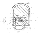
(発光装置)
実施の形態1の発光装置は、サファイア基板1の上部に積層された半導体層2と、該半導体層2に形成された正負の電極3から延びる導電性ワイヤ14で導電接続されたリードフレーム13と、該サファイア基板1と該半導体層2とから構成される発光素子10の外周を覆うようにリードフレーム13aのカップ内に設けられた蛍光体11とコーティング部材12と、該蛍光体11及び該リードフレーム13の外周面を覆うモールド部材15と、から構成されている。
【0042】
サファイア基板1上に半導体層2が形成され、該半導体層2の同一平面側に正負の電極3が形成されている。前記半導体層2には、発光層(図示しない)が設けられており、この発光層から出力される発光ピーク波長は、紫外から青色領域の500nm以下近傍の発光スペクトルを有する。
【0043】
この発光素子10をダイボンダーにセットし、カップが設けられたリードフレーム13aにフェイスアップしてダイボンド(接着)する。ダイボンド後、リードフレーム13をワイヤーボンダーに移送し、発光素子の負電極3をカップの設けられたリードフレーム13aに金線でワイヤーボンドし、正電極3をもう一方のリードフレーム13bにワイヤーボンドする。
【0044】
次に、モールド装置に移送し、モールド装置のディスペンサーでリードフレーム13のカップ内に蛍光体11及びコーティング部材12を注入する。蛍光体11とコーティング部材12とは、あらかじめ所望の割合に均一に混合しておく。
【0045】
蛍光体11注入後、あらかじめモールド部材15が注入されたモールド型枠の中にリードフレーム13を浸漬した後、型枠をはずして樹脂を硬化させ、図1に示すような砲弾型の発光装置とする。
【0046】
(発光装置)
上記の実施の形態1の発光装置と異なる実施の形態2の発光装置についての具体的構成について詳述する。図2は、本発明に係る発光装置を示す図である。実施の形態2の発光装置は、表面実装型の発光装置を形成する。発光素子101は、紫外光励起の窒化物半導体発光素子を用いることができる。また、発光素子101は、青色光励起の窒化物半導体発光素子も用いることもできる。ここでは、紫外光励起の発光素子101を例にとって、説明する。発光素子101は、発光層として発光ピーク波長が約370nmのInGaN半導体を有する窒化物半導体発光素子を用いる。より具体的なLEDの素子構造としてサファイア基板上に、アンドープの窒化物半導体であるn型GaN層、Siドープのn型電極が形成されn型コンタクト層となるGaN層、アンドープの窒化物半導体であるn型GaN層、窒化物半導体であるn型AlGaN層、次に発光層を構成するInGaN層の単一量子井戸構造としてある。発光層上にはMgがドープされたp型クラッド層としてAlGaN層、Mgがドープされたp型コンタクト層であるGaN層を順次積層させた構成としてある。(なお、サファイア基板上には低温でGaN層を形成させバッファ層とさせてある。また、p型半導体は、成膜後400℃以上でアニールさせてある。)。エッチングによりサファイア基板上の窒化物半導体に同一面側で、pn各コンタクト層表面を露出させる。露出されたn型コンタクト層の上にn電極を帯状に形成し、切除されずに残ったp型コンタクト層のほぼ全面に、金属薄膜から成る透光性p電極が形成され、さらに透光性p電極の上にはn電極と平行に台座電極がスパッタリング法を用いて形成されている。
【0047】
次に、中央部に凹部を有し、且つ前記凹部の両側にコバール製のリード電極102が気密絶縁的に挿入固定されたベース部とからなるコバール製パッケージ105を用いる。前記パッケージ105及びリード電極102の表面にはNi/Ag層が設けられている。パッケージ105の凹部内に、Ag−Sn合金にて上述の発光素子101をダイボンドする。このように構成することにより、発光装置の構成部材を全て無機物とすることができ、発光素子101から放出される発光が紫外領域或いは可視光の短波長領域であったとしても飛躍的に信頼性の高い発光装置が得られる。
【0048】
次に、ダイボンドされた発光素子101の各電極と、パッケージ凹部底面から露出された各リード電極102とをそれぞれAgワイヤ104にて電気的導通を取る。パッケージの凹部内の水分を十分に排除した後、中央部にガラス窓部107を有するコバール製リッド106にて封止しシーム溶接を行う。ガラス窓部には、あらかじめニトロセルロース90wt%とγ−アルミナ10wt%からなるスラリーに対してCaSi2O2N2:Eu、(Y0.8Gd0.2)3Al5O12:Ce等の蛍光体108を含有させ、リッド106の透光性窓部107の背面に塗布し、220℃にて30分間加熱硬化させることにより色変換部材を構成してある。こうして形成された発光装置を発光させると白色が高輝度に発光可能な発光ダイオードとすることができる。これによって色度調整が極めて簡単で量産性、信頼性に優れた発光装置とすることできる。以下、本発明の各構成について詳述する。
【0049】
以下、本発明に係る発光装置の構成部材について詳述する。
【0050】
(蛍光体11、108)
蛍光体11、108は、オキシ窒化物蛍光体が含まれている。また、蛍光体11、108は、オキシ窒化物蛍光体と第2の蛍光体とを組み合わせたものも使用することができる。本発明に係るオキシ窒化物蛍光体は、賦活剤に希土類元素を用いており、Be、Mg、Ca、Sr、Ba、Znからなる群から選ばれる少なくとも1種以上である第II族元素と、C、Si、Ge、Sn、Ti、Zr、Hfからなる群から選ばれる少なくとも1種以上である第IV族元素と、を少なくとも含有する。該元素の組合せは任意であるが、以下の組成のものを使用することが好ましい。該オキシ窒化物蛍光体は、LXMYOZN((2/3)X+(4/3)Y−(2/3)Z):R、又は、LXMYQTOZN((2/3)X+(4/3)Y+T−(2/3)Z):R(Lは、Be、Mg、Ca、Sr、Ba、Znからなる群から選ばれる少なくとも1種以上である第II族元素である。Mは、C、Si、Ge、Sn、Ti、Zr、Hfからなる群から選ばれる少なくとも1種以上である第IV族元素である。Qは、B、Al、Ga、Inからなる群から選ばれる少なくとも1種以上である第III族元素である。Oは、酸素元素である。Nは、窒素元素である。Rは、希土類元素である。0.5<X<1.5、1.5<Y<2.5、0<T<0.5、1.5<Z<2.5である。)の一般式で表される。前記X、前記Y、前記Zは、該範囲で高い輝度を示す。そのうち特に、一般式中、前記X、前記Y、前記Zが、X=1、Y=2、Z=2で表されるオキシ窒化物蛍光体は高い輝度を示すため特に好ましい。但し、上記範囲に限定されず、任意のものも使用できる。具体的にはCaSi2O2N2:Eu、SrSi2O2N2:Eu、BaSi2O2N2:Eu、ZnSi2O2N2:Eu、CaGe2O2N2:Eu、SrGe2O2N2:Eu、BaGe2O2N2:Eu、ZnGe2O2N2:Eu、Ca0.5Sr0.5Si2O2N2:Eu、Ca0.5Ba0.5Si2O2N2:Eu、Ca0.5Zn0.5Si2O2N2:Eu、Ca0.5Be0.5Si2O2N2:Eu、Sr0.5Ba0.5Si2O2N2:Eu、Ca0.8Mg0.2Si2O2N2:Eu、Sr0.8Mg0.2Si2O2N2:Eu、Ca0.5Mg0.5Si2O2N2:Eu、Sr0.5Mg0.5Si2O2N2:Eu、CaSi2B0.1O2N2:Eu、SrSi2B0.1O2N2:Eu、BaSi2B0.1O2N2:Eu、ZnSi2B0.1O2N2:Eu、CaGe2B0.01O2N2:Eu、SrGe2Ga0.01O2N2:Eu、BaGe2In0.01O2N2:Eu、ZnGe2Al0.05O2N2:Eu、Ca0.5Sr0.5Si2B0.3O2N2:Eu、CaSi2.5O1.5N3:Eu、SrSi2.5O1.5N3:Eu、BaSi2.5O1.5N3:Eu、Ca0.5Ba0.5Si2.5O1.5N3:Eu、Ca0.5Sr0.5Si2.5O1.5N3:Eu、Ca1.5Si2.5O2.5N2.7:Eu、Sr1.5Si2.5O2.5N2.7:Eu、Ba1.5Si2.5O2.5N2.7:Eu、Ca1.0Ba0.5Si2.5O1.5N3:Eu、Ca1.0Sr0.5Si2.5O1.5N3:Eu、Ca0.5Si1.5O1.5N1.7:Eu、Sr0.5Si1.5O1.5N1.7:Eu、Ba0.5Si1.5O1.5N1.7:Eu、Ca0.3Ba0.2Si2.5O1.5N3:Eu、Ca0.2Sr0.3Si2.5O1.5N3:Eu等で表されるオキシ窒化物蛍光体を使用することできる。また、ここで示すように、本オキシ窒化物蛍光体は、OとNとの比を変化させることで、色調や輝度を調節することができる。また、(L+M)/(O+N)で示す陽イオンと陰イオンのモル比を変化させることでも、微妙に発光スペクトルや強度を調整することも可能である。これは、例えば、真空などの処理を施し、NやOを脱離させること等により可能であるが、この方法には、限定されない。このオキシ窒化物蛍光体の組成中には、Li、Na、K、Rb、Cs、Mn、Re、Cu、Ag、Auの少なくとも1種以上含有されていてもよい。これらを添加することにより輝度、量子効率等の発光効率を調整することができるからである。また、その他の元素も特性を損なわない程度に入っていても良い。但し、本発明は、この実施の形態及び実施例に限定されない。
【0051】
Lは、Mg、Ca、Sr、Ba、Znからなる群から選ばれる少なくとも1種以上である第II族元素である。つまり、Ca、Sr等を単体で用いてもよいが、CaとSr、CaとBa、SrとBa、CaとMg等、種々組合せを変えることもできる。SrとCaとの混合物は、所望により配合比を変えることができる。
【0052】
Mは、C、Si、Ge、Sn、Ti、Hfからなる群から選ばれる少なくとも1種以上である第IV族元素である。Mも、Si、Ge等を単体で用いてもよいが、SiとGe、SiとC等、種々組合せを変えることもできる。該元素を用いることができるが、特にSi、Geを用いることが好ましい。これにより安価で結晶性の良好な蛍光体を提供することができるからである。
【0053】
Rは、希土類元素である。具体的には、Rは、La、Ce、Pr、Nd、Sm、Eu、Gd、Tb、Dy、Ho、Er、Tm、Yb、Lrである。これら希土類元素のうち、Euが好ましい。また、Euと、希土類元素から選ばれる少なくとも1以上の元素と、を含んでいるものも使用することができる。Rは、Euが70%以上含有されていることが好ましい。
【0054】
発光中心に希土類元素であるユウロピウムEuを用いる。本発明では、Euを用いて説明するが、これに限定されない。ユウロピウムは、主に2価と3価のエネルギー準位を持つ。本発明の蛍光体は、母体のアルカリ土類金属系窒化ケイ素に対して、Eu2+を付活剤として用いる。Eu2+は、酸化されやすく、一般に3価のEu2O3の組成で市販されている。
【0055】
母体材料として、主成分のL、Mも、それぞれの化合物を使用することができる。これら主成分のL、Mは、金属、酸化物、イミド、アミド、窒化物及び各種塩類などを用いることができる。また、あらかじめ主成分のL、Mの元素を混合し、使用してもよい。
【0056】
Qは、B、Al、Ga、Inからなる群から選ばれる少なくとも1種以上である第III族元素である。Qも、金属、酸化物、イミド、アミド、窒化物及び各種塩類などを用いることができる。例えば、B2O6、H3BO3、Al2O3、Al(NO3)3・9H2O、AlN、GaCl3、InCl3等である。
【0057】
Lの窒化物、Mの窒化物、Mの酸化物を母体材料として、混合する。該母体材料中に、Euの酸化物を付活剤として混入する。これらを所望量計り、均一になるまで混合する。特に、該母体材料のLの窒化物、Mの窒化物、Mの酸化物は、0.5<Lの窒化物<1.5、0.25<Mの窒化物<1.75、2.25<Mの酸化物<3.75、のモル比で混合されていることが好ましい。これらの母体材料を、LXMYOZN((2/3)X+Y−(2/3)Z−α):R又はLXMYQTOZN((2/3)X+Y+T−(2/3)Z−α):Rの組成比となるように、所定量を秤量して混合する。
【0058】
(オキシ窒化物蛍光体の製造方法)
次に、本発明に係るオキシ窒化物蛍光体、CaSi2O2N2:Euの製造方法を説明するが、本製造方法に限定されない。
【0059】
まず所定配合比となるように、Caの窒化物、Siの窒化物、Siの酸化物、Euの酸化物を混合する。
【0060】
あらかじめCaの窒化物、Siの窒化物、Siの酸化物、Euの酸化物を準備する。これら原料は、精製したものを用いる方が良いが、市販のものを用いても良い。具体的には、原料のCaを粉砕する。原料のCaは、単体を使用することが好ましいが、イミド化合物、アミド化合物、CaOなどの化合物を使用することもできる。また原料Caは、B、Gaなどを含有するものでもよい。原料のCaは、アルゴン雰囲気中、グローブボックス内で粉砕を行う。粉砕により得られたCaは、平均粒径が約0.1μmから15μmであることが好ましいが、この範囲に限定されない。Caの純度は、2N以上であることが好ましいが、これに限定されない。
【0061】
原料のCaを、窒素雰囲気中で窒化する。この反応式を、化1に示す。
【0062】
【化1】
3Ca + N2 → Ca3N2
Caを、窒素雰囲気中、600〜900℃、約5時間、窒化して、Caの窒化物を得ることができる。Caの窒化物は、高純度のものが好ましいが、市販のものも使用することができる。
【0063】
Caの窒化物を粉砕する。Caの窒化物を、アルゴン雰囲気中、若しくは、窒素雰囲気中、グローブボックス内で粉砕を行う。
【0064】
原料のSiを粉砕する。原料のSiは、単体を使用することが好ましいが、窒化物化合物、イミド化合物、アミド化合物などを使用することもできる。例えば、Si3N4、Si(NH2)2、Mg2Si、Ca2Si、SiCなどである。原料のSiの純度は、3N以上のものが好ましいが、B、Gaなどが含有されていてもよい。Siも、原料のCaと同様に、アルゴン雰囲気中、若しくは、窒素雰囲気中、グローブボックス内で粉砕を行う。Si化合物の平均粒径は、約0.1μmから15μmであることが好ましい。
【0065】
原料のSiを、窒素雰囲気中で窒化する。この反応式を、化2に示す。
【0066】
【化2】
3Si + 2N2 → Si3N4
ケイ素Siも、窒素雰囲気中、800〜1200℃、約5時間、窒化して、窒化ケイ素を得る。本発明で使用する窒化ケイ素は、高純度のものが好ましいが、市販のものも使用することができる。
【0067】
同様に、Siの窒化物を粉砕する。
【0068】
Siの酸化物であるSiO2は、市販のものを用いる(和光純薬製 Silicon Dioxide 99.9%,190-09072)。
【0069】
以上のようにして精製又は製造を行った原料を所定のモル量を秤量する。該秤量した原料を、混合する。
【0070】
次に、Caの窒化物、Siの窒化物、Siの酸化物、Euの酸化物の混合物をアンモニア雰囲気中、約1500℃で、焼成する。当該混合物を坩堝に投入し、焼成を行う。
【0071】
混合及び焼成により、CaSi2O2N2:Euで表されるオキシ窒化物蛍光体を得ることができる。この焼成による基本構成元素の反応式を、化3に示す。
【0072】
【化3】

ただし、この組成は、配合比率より推定される代表組成であり、その比率の近傍では、実用に耐える十分な特性を有する。また、各原料の配合比率を変更することにより、目的とする蛍光体の組成を変更することができる。
【0074】
焼成は、管状炉、小型炉、高周波炉、メタル炉などを使用することができる。焼成温度は、特に限定されないが、1200から1700℃の範囲で焼成を行うことが好ましく、1400から1700℃の焼成温度が、さらに好ましい。蛍光体11の原料は、窒化ホウ素(BN)材質の坩堝、ボートを用いて焼成を行うことが好ましい。窒化ホウ素材質の坩堝の他に、アルミナ(Al2O3)材質の坩堝を使用することもできる。
【0075】
また、還元雰囲気は、窒素雰囲気、窒素−水素雰囲気、アンモニア雰囲気、アルゴン等の不活性ガス雰囲気等である。
【0076】
以上の製造方法を使用することにより、目的とするオキシ窒化物蛍光体を得ることが可能である。
【0077】
なお、CaXSiYBTOZN((2/3)X+Y+T−(2/3)Z−α):Euで表されるオキシ窒化物蛍光体は、以下のようにして製造することができる。
【0078】
あらかじめ、Euの酸化物に、Bの化合物H3BO3を乾式混合する。Euの化合物として、酸化ユウロピウムを使用するが、前述の他の構成元素と同様、金属ユウロピウム、窒化ユウロピウムなども使用可能である。このほか、原料のEuは、イミド化合物、アミド化合物を用いることもできる。酸化ユウロピウムは、高純度のものが好ましいが、市販のものも使用することができる。Bの化合物を乾式混合するが、湿式混合することもできる。これらの混合物は、酸化されやすいものもあるため、Ar雰囲気中、又は、窒素雰囲気中、グローブボックス内で、混合を行う。
【0079】
Bの化合物H3BO3を例にとって、オキシ窒化物蛍光体の製造方法を説明するが、B以外の成分構成元素には、Li、Na、K等があり、これらの化合物、例えば、LiOH・H2O、Na2CO3、K2CO3、RbCl、CsCl、Mg(NO3)2、CaCl2・6H2O、SrCl2・6H2O、BaCl2・2H2O、TiOSO4・H2O、ZrO(NO3)2、HfCl4、MnO2、ReCl5、Cu(CH3COO)2・H2O、AgNO3、HAuCl4・4H2O、Zn(NO3)2・6H2O、GeO2、Sn(CH3COO)2等を使用することができる。
【0080】
EuとBの混合物を粉砕する。粉砕後のEuとBの混合物の平均粒径は、約0.1μmから15μmであることが好ましい。
【0081】
上記粉砕を行った後、前述のCaSi2O2N2:Euの製造工程とほぼ同様に、Caの窒化物、Siの窒化物、Siの酸化物、Bを含有するEuの酸化物、を混合する。該混合後、焼成を行い、目的のオキシ窒化物蛍光体を得ることができる。
【0082】
(第2の蛍光体11、108)
蛍光体11、108中には、オキシ窒化物蛍光体と共に、第2の蛍光体が含まれている。第2の蛍光体としては、Eu等のランタノイド系、Mn等の遷移金属系の元素により主に付活されるアルカリ土類ハロゲンアパタイト蛍光体、アルカリ土類金属ホウ酸ハロゲン蛍光体、アルカリ土類金属アルミン酸塩蛍光体、アルカリ土類ケイ酸塩、アルカリ土類硫化物、アルカリ土類チオガレート、アルカリ土類窒化ケイ素、ゲルマン酸塩、又は、Ce等のランタノイド系元素で主に付活される希土類アルミン酸塩、希土類ケイ酸塩、又は、Eu等のランタノイド系元素で主に賦活される有機及び有機錯体等から選ばれる少なくともいずれか1以上であることが好ましい。具体例として、下記の蛍光体を使用することができるが、これに限定されない。
【0083】
Eu等のランタノイド系、Mn等の遷移金属系の元素により主に付活されるアルカリ土類ハロゲンアパタイト蛍光体には、M5(PO4)3X:R(Mは、Sr、Ca、Ba、Mg、Znから選ばれる少なくとも1種以上である。Xは、F、Cl、Br、Iから選ばれる少なくとも1種以上である。Rは、Eu、Mn、EuとMn、のいずれか1以上である。)などがある。
【0084】
アルカリ土類金属ホウ酸ハロゲン蛍光体には、M2B5O9X:R(Mは、Sr、Ca、Ba、Mg、Znから選ばれる少なくとも1種以上である。Xは、F、Cl、Br、Iから選ばれる少なくとも1種以上である。Rは、Eu、Mn、EuとMn、のいずれか1以上である。)などがある。
【0085】
アルカリ土類金属アルミン酸塩蛍光体には、SrAl2O4:R、Sr4Al14O25:R、CaAl2O4:R、BaMg2Al16O27:R、BaMg2Al16O12:R、BaMgAl10O17:R(Rは、Eu、Mn、EuとMn、のいずれか1以上である。)などがある。
【0086】
アルカリ土類硫化物蛍光体には、La2O2S:Eu、Y2O2S:Eu、Gd2O2S:Euなどがある。
【0087】
Ce等のランタノイド系元素で主に賦活される希土類アルミン酸塩蛍光体には、Y3Al5O12:Ce、(Y0.8Gd0.2)3Al5O12:Ce、Y3(Al0.8Ga0.2)5O12:Ce、(Y,Gd)3(Al,Ga)5O12の組成式で表されるYAG系蛍光体などがある。
【0088】
その他の蛍光体には、ZnS:Eu、Zn2GeO4:Mn、MGa2S4:Eu(Mは、Sr、Ca、Ba、Mg、Znから選ばれる少なくとも1種以上である。Xは、F、Cl、Br、Iから選ばれる少なくとも1種以上である。)などがある。また、M2Si5N8:Eu、MSi7N10:Eu、M1.8Si5O0.2N8:Eu、M0.9Si7O0.1N10:Eu(Mは、Sr、Ca、Ba、Mg、Znから選ばれる少なくとも1種以上である。)などもある。
【0089】
上述の第2の蛍光体は、所望に応じてEuに代えて、又は、Euに加えてTb、Cu、Ag、Au、Cr、Nd、Dy、Co、Ni、Tiから選択される1種以上を含有させることもできる。
【0090】
また、上記蛍光体以外の蛍光体であって、同様の性能、効果を有する蛍光体も使用することができる。
【0091】
これらの第2の蛍光体は、発光素子10、101の励起光により、黄色、赤色、緑色、青色に発光スペクトルを有する蛍光体を使用することができるほか、これらの中間色である黄色、青緑色、橙色などに発光スペクトルを有する蛍光体も使用することができる。これらの第2の蛍光体を第1の蛍光体と組み合わせて使用することにより、種々の発光色を有する発光装置を製造することができる。
【0092】
例えば、第1の蛍光体である緑色から黄色に発光するCaSi2O2N2:Eu、又はSrSi2O2N2:Euと、第2の蛍光体である青色に発光する(Sr,Ca)5(PO4)3Cl:Eu、赤色に発光する(Ca,Sr)2Si5N8:Euと、からなる蛍光体11、108を使用することによって、演色性の良好な白色に発光する発光装置を提供することができる。これは、色の三源色である赤・青・緑を使用しているため、第1の蛍光体及び第2の蛍光体の配合比を変えることのみで、所望の白色光を実現することができる。
【0093】
上記蛍光体11、108の粒径は、1μm〜20μmの範囲が好ましく、より好ましくは2μm〜8μmである。特に、5μm〜8μmが好ましい。2μmより小さい粒径を有する蛍光体は、凝集体を形成しやすい傾向にある。一方、5μm〜8μmの粒径範囲の蛍光体は、光の吸収率及び変換効率が高い。このように、光学的に優れた特徴を有する粒径の大きな蛍光体を含有させることにより、発光装置の量産性が向上する。
【0094】
ここで粒径は、空気透過法で得られる平均粒径を指す。具体的には、気温25℃、湿度70%の環境下において、1cm3分の試料を計り取り、専用の管状容器にパッキングした後、一定圧力の乾燥空気を流し、差圧から比表面積を読みとり、平均粒径に換算した値である。本発明で用いられる蛍光体の平均粒径は2μm〜8μmの範囲であることが好ましい。また、この平均粒径値を有する蛍光体が、頻度高く含有されていることが好ましい。また、粒度分布も狭い範囲に分布しているものが好ましく、特に、微粒子2μm以下の少ないものが好ましい。このように粒径、及び粒度分布のバラツキが小さい蛍光体を用いることにより、より色ムラが抑制され、良好な色調を有する発光装置が得られる。
【0095】
発光装置2における蛍光体108の配置場所は発光素子101との位置関係において種々の場所に配置することができる。例えば、発光素子101を被覆するモールド材料中に、蛍光体108を含有させることができる。また、発光素子101と蛍光体108とを、間隙をおいて配置しても良いし、発光素子101の上部に蛍光体108を、直接載置しても良い。
【0096】
(コーティング部材12、109)
蛍光体11、108は、有機材料である樹脂や無機材料であるガラスなど種々のコーティング部材(バインダー)を用いて、付着させることができる。コーティング部材12、109は、蛍光体11、108を発光素子10、101や窓部107等に固着させるためのバインダーとしての役割を有することもある。コーティング部材(バインダー)として有機物を使用する場合、具体的材料として、エポキシ樹脂、アクリル樹脂、シリコーンなどの耐候性に優れた透明樹脂が好適に用いられる。特に、シリコーンを用いると、信頼性に優れ、且つ蛍光体11、108の分散性を向上させることができ好ましい。
【0097】
また、コーティング部材(バインダー)12、109として、窓部107の熱膨張率と近似である無機物を使用すると、蛍光体108を良好に前記窓部107に密着させることができ好ましい。具体的方法として、沈降法やゾル−ゲル法、スプレー法等を用いることができる。例えば、蛍光体11、108に、シラノール(Si(OEt)3OH)、及びエタノールを混合してスラリーを形成し、該スラリーをノズルから吐出させた後、300℃にて3時間加熱してシラノールをSiO2とし、蛍光体を所望の場所に固着させることができる。
【0098】
また、無機物である結着剤をコーティング部材(バインダー)12、109として用いることもできる。結着剤とは、いわゆる低融点ガラスであり、微細な粒子であり、且つ紫外から可視領域のふく射線に対して吸収が少なく、コーティング部材(バインダー)12、109中にて極めて安定であることが好ましい。
【0099】
また、粒径の大きな蛍光体をコーティング部材(バインダー)12、109に付着させる場合、融点が高くても粒子が超微粉体である結着剤、例えば、シリカ、アルミナ、あるいは沈殿法で得られる細かい粒度のアルカリ土類金属のピロリン酸塩、正りん酸塩などを使用することが好ましい。これらの結着剤は、単独、若しくは互いに混合して用いることができる。
【0100】
ここで、上記結着剤の塗布方法について述べる。結着剤は、結着効果を十分に高めるため、ビヒクル中に湿式粉砕して、スラリー状にして、結着剤スラリーとして用いることが好ましい。前記ビヒクルとは、有機溶媒あるいは脱イオン水に少量の粘結剤を溶解して得られる高粘度溶液である。例えば、有機溶媒である酢酸ブチルに対して粘結剤であるニトロセルロースを1wt%含有させることにより、有機系ビヒクルが得られる。
【0101】
このようにして得られた結着剤スラリーに、蛍光体11、108を含有させて塗布液を作製する。塗布液中のスラリーの添加量は、塗布液中の蛍光体量に対してスラリー中の結着剤の総量が、1〜3%wt程度とすることができる。光束維持率の低下を抑制するため、結着剤の添加量が少ない方が好ましい。
【0102】
前記塗布液を前記窓部107の背面に塗布する。その後、温風あるいは熱風を吹き込み乾燥させる。最後に400℃〜700℃の温度でベーキングを行い、前記ビヒクルを飛散させる。これにより所望の場所に蛍光体層が結着剤にて付着される。
【0103】
(発光素子10、101)
本発明において発光素子10、101は、蛍光体を効率よく励起可能な発光波長を発光できる発光層を有する半導体発光素子が好ましい。このような半導体発光素子の材料として、BN、SiC、ZnSeやGaN、InGaN、InAlGaN、AlGaN、BAlGaN、BInAlGaNなど種々の半導体を挙げることができる。同様に、これらの元素に不純物元素としてSiやZnなどを含有させ発光中心とすることもできる。蛍光体11、108を効率良く励起できる紫外領域から可視光の短波長を効率よく発光可能な発光層の材料として特に、窒化物半導体(例えば、AlやGaを含む窒化物半導体、InやGaを含む窒化物半導体としてInXAlYGa1−X−YN、0≦X、0≦Y、X+Y≦1)がより好適に挙げられる。
【0104】
また、半導体の構造としては、MIS接合、PIN接合やpn接合などを有するホモ構造、ヘテロ構造あるいはダブルへテロ構成のものが好適に挙げられる。半導体層の材料やその混晶比によって発光波長を種々選択することができる。また、半導体活性層を量子効果が生ずる薄膜に形成させた単一量子井戸構造や多重量子井戸構造とすることでより出力を向上させることもできる。
【0105】
発光素子10、101に、窒化物半導体を使用した場合、半導体用基板にはサファイア、スピネル、SiC、Si、ZnO、GaAs、GaN等の材料が好適に用いられる。結晶性の良い窒化物半導体を量産性よく形成させるためにはサファイア基板を利用することが好ましい。このサファイア基板上にHVPE法やMOCVD法などを用いて窒化物半導体を形成させることができる。サファイア基板上にGaN、AlN、GaAIN等の低温で成長させ非単結晶となるバッファ層を形成しその上にpn接合を有する窒化物半導体を形成させる。
【0106】
窒化物半導体を使用したpn接合を有する紫外領域を効率よく発光可能な発光素子例として、バッファ層上に、サファイア基板のオリフラ面と略垂直にSiO2をストライプ状に形成する。ストライプ上にHVPE法を用いてGaNをELOG(Epitaxial Lateral Over Grows GaN)成長させる。続いて、MOCVD法により、n型窒化ガリウムで形成した第1のコンタクト層、n型窒化アルミニウム・ガリウムで形成させた第1のクラッド層、窒化インジウム・アルミニウム・ガリウムの井戸層と窒化アルミニウム・ガリウムの障壁層を複数積層させた多重量子井戸構造とされる活性層、p型窒化アルミニウム・ガリウムで形成した第2のクラッド層、p型窒化ガリウムで形成した第2のコンタクト層を順に積層させたダブルへテロ構成などの構成が挙げられる。活性層をリッジストライプ形状としガイド層で挟むと共に共振器端面を設け本発明に利用可能な半導体レーザー素子とすることもできる。
【0107】
窒化物半導体は、不純物をドープしない状態でn型導電性を示す。発光効率を向上させるなど所望のn型窒化物半導体を形成させる場合は、n型ドーパントとしてSi、Ge、Se、Te、C等を適宜導入することが好ましい。一方、p型窒化物半導体を形成させる場合は、p型ドーパントであるZn、Mg、Be、Ca、Sr、Ba等をドープさせることが好ましい。窒化物半導体は、p型ドーパントをドープしただけではp型化しにくいためp型ドーパント導入後に、炉による加熱やプラズマ照射等により低抵抗化させることが好ましい。サファイア基板をとらない場合は、第1のコンタクト層の表面までp型側からエンチングさせコンタクト層を露出させる。各コンタクト層上にそれぞれ電極形成後、半導体ウエハーからチップ状にカットさせることで窒化物半導体からなる発光素子を形成させることができる。
【0108】
本発明の発光装置において、量産性よく形成させるためには、蛍光体11、108を発光素子10、101に固着する際に、樹脂を利用して形成することが好ましい。この場合、蛍光体11、108からの発光波長と透光性樹脂の劣化等を考慮して、発光素子10、101は紫外域に発光スペクトルを有し、その発光ピーク波長は、360nm以上420nm以下のものや、450nm以上470nm以下のものを使用することが好ましい。
【0109】
ここで、本発明で用いられる半導体発光素子10、101は、不純物濃度1017〜1020/cm3で形成されるn型コンタクト層のシート抵抗と、透光性p電極のシート抵抗とが、Rp≧Rnの関係となるように調節されていることが好ましい。n型コンタクト層は、例えば膜厚3〜10μm、より好ましくは4〜6μmに形成されると好ましく、そのシート抵抗は10〜15Ω/□と見積もられることから、このときのRpは前記シート抵抗値以上のシート抵抗値を有するように薄膜に形成するとよい。また、透光性p電極は、膜厚が150μm以下の薄膜で形成されていてもよい。
【0110】
また、透光性p電極が、金および白金族元素の群から選択された1種と、少なくとも1種の他の元素とから成る多層膜または合金で形成される場合には、含有されている金または白金族元素の含有量により透光性p電極のシート抵抗の調整をすると安定性および再現性が向上される。金または金属元素は、本発明に使用する半導体発光素子の波長領域における吸収係数が高いので、透光性p電極に含まれる金又は白金族元素の量は少ないほど透過性がよくなる。従来の半導体発光素子はシート抵抗の関係がRp≦Rnであったが、本発明ではRp≧Rnであるので、透光性p電極は従来のものと比較して薄膜に形成されることとなるが、このとき金または白金族元素の含有量を減らすことで薄膜化が容易に行える。
【0111】
上述のように、本発明で用いられる半導体発光素子10、101は、n型コンタクト層のシート抵抗RnΩ/□と、透光性p電極のシート抵抗RpΩ/□とが、Rp≧Rnの関係を成していることが好ましい。半導体発光素子10、101として形成した後にRnを測定するのは難しく、RpとRnとの関係を知るのは実質上不可能であるが、発光時の光強度分布の状態からどのようなRpとRnとの関係になっているのかを知ることができる。
【0112】
透光性p電極とn型コンタクト層とがRp≧Rnの関係であるとき、前記透光性p電極上に接して延長伝導部を有するp側台座電極を設けると、さらなる外部量子効率の向上を図ることができる。延長伝導部の形状及び方向に制限はなく、延長伝導部が衛線上である場合、光を遮る面積が減るので好ましいが、メッシュ状でもよい。また形状は、直線状以外に、曲線状、格子状、枝状、鉤状でもよい。このときp側台座電極の総面積に比例して遮光効果が増大するため、遮光効果が発光増強効果を上回らないように延長導電部の線幅及び長さを設計するのがよい。
【0113】
(発光素子10、101)
発光素子10、101は、上述の紫外発光の発光素子と異なる青色系に発光する発光素子を使用することもできる。青色系に発光する発光素子10、101は、III族窒化物系化合物発光素子であることが好ましい。発光素子10、101は、例えばサファイア基板1上にGaNバッファ層を介して、Siがアンドープのn型GaN層、Siがドープされたn型GaNからなるn型コンタクト層、アンドープGaN層、多重量子井戸構造の発光層(GaN障壁層/InGaN井戸層の量子井戸構造)、Mgがドープされたp型GaNからなるp型GaNからなるpクラッド層、Mgがドープされたp型GaNからなるp型コンタクト層が順次積層された積層構造を有し、以下のように電極が形成されている。但し、この構成と異なる発光素子も使用できる。
【0114】
pオーミック電極は、p型コンタクト層上のほぼ全面に形成され、そのpオーミック電極上の一部にpパッド電極が形成される。
【0115】
また、n電極は、エッチングによりp型コンタクト層からアンドープGaN層を除去してn型コンタクト層の一部を露出させ、その露出された部分に形成される。
【0116】
なお、本実施の形態では、多重量子井戸構造の発光層を用いたが、本発明は、これに限定されるものではなく、例えば、InGaNを利用した単一量子井戸構造としても良いし、Si、ZnがドープされたGaNを利用しても良い。
【0117】
また、発光素子10、101の発光層は、Inの含有量を変化させることにより、420nmから490nmの範囲において主発光ピーク波長を変更することができる。また、発光ピーク波長は、上記範囲に限定されるものではなく、360〜550nmに発光ピーク波長を有しているものを使用することができる。
【0118】
(コーティング部材12、109)
コーティング部材12(光透光性材料)は、リードフレーム13のカップ内に設けられるものであり発光素子10の発光を変換する蛍光体11と混合して用いられる。コーティング部材12の具体的材料としては、エポキシ樹脂、ユリア樹脂、シリコーン樹脂などの温度特性、耐候性に優れた透明樹脂、シリカゾル、ガラス、無機バインダーなどが用いられる。また、蛍光体と共に拡散剤、チタン酸バリウム、酸化チタン、酸化アルミニウムなどを含有させても良い。また、光安定化剤や着色剤を含有させても良い。
【0119】
(リードフレーム13)
リードフレーム13は、マウントリード13aとインナーリード13bとから構成される。
【0120】
マウントリード13aは、発光素子10を配置させるものである。マウントリード13aの上部は、カップ形状になっており、カップ内に発光素子10をダイボンドし、該発光素子10の外周面を、カップ内を前記蛍光体11と前記コーティング部材12とで覆っている。カップ内に発光素子10を複数配置しマウントリード13aを発光素子10の共通電極として利用することもできる。この場合、十分な電気伝導性と導電性ワイヤ14との接続性が求められる。発光素子10とマウントリード13aのカップとのダイボンド(接着)は、熱硬化性樹脂などによって行うことができる。熱硬化性樹脂としては、エポキシ樹脂、アクリル樹脂、イミド樹脂などが挙げられる。また、フェースダウン発光素子10などによりマウントリード13aとダイボンドすると共に電気的接続を行うには、Ag―エースと、カーボンペースト、金属バンプなどを用いることができる。また、無機バインダーを用いることもできる。
【0121】
インナーリード13bは、マウントリード13a上に配置された発光素子10の電極3から延びる導電性ワイヤ14との電気的接続を図るものである。インナーリード13bは、マウントリード13aとの電気的接触によるショートを避けるため、マウントリード13aから離れた位置に配置することが好ましい。マウントリード13a上に複数の発光素子10を設けた場合は、各導電性ワイヤ同士が接触しないように配置できる構成にする必要がある。インナーリード13bは、マウントリード13aと同様の材質を用いることが好ましく、鉄、銅、鉄入り銅、金、白金、銀などを用いることができる。
【0122】
(導電性ワイヤ)
導電性ワイヤ14は、発光素子10の電極3とリードフレーム13とを電気的に接続するものである。導電性ワイヤ14は、電極3とオーミック性、機械的接続性、電気導電性及び熱伝導性が良いものが好ましい。導電性ワイヤ14の具体的材料としては、金、銅、白金、アルミニウムなどの金属及びそれらの合金などが好ましい。
【0123】
(モールド部材)
モールド部材15は、発光素子10、蛍光体11、コーティング部材12、リードフレーム13及び導電性ワイヤ14などを外部から保護するために設けられている。モールド部材15は、外部からの保護目的の他に、視野角を広げたり、発光素子10からの指向性を緩和したり、発光を収束、拡散させたりする目的も併せ持っている。これらの目的を達成するためモールド部材は、所望の形状にすることができる。また、モールド部材15は、凸レンズ形状、凹レンズ形状の他、複数積層する構造であっても良い。モールド部材15の具体的材料としては、エポキシ樹脂、ユリア樹脂、シリコーン樹脂、シリカゾル、ガラスなどの透光性、耐候性、温度特性に優れた材料を使用することができる。モールド部材15には、拡散剤、着色剤、紫外線吸収剤や蛍光体を含有させることもできる。拡散剤としては、チタン酸バリウム、酸化チタン、酸化アルミニウム等が好ましい。コーティング部材12との材質の反発性を少なくするため、屈折率を考慮するため、同材質を用いることが好ましい。
【0124】
以下、本発明に係る蛍光体、発光装置について実施例を挙げて説明するが、この実施例に限定されるものではない。
【0125】
なお、温度特性は、25℃の発光輝度を100%とする相対輝度で示す。粒径は、前述の平均粒径を示し、F.S.S.S.No.(Fisher Sub Sieve Sizer's No.)という空気透過法による値である。
【0126】
【実施例】
以下、本発明の実施例について詳述する。
【0127】
(蛍光体)
<実施例1乃至5>
表1は、本発明に係るオキシ窒化物蛍光体の実施例1乃至5の特性を示す。
【0128】
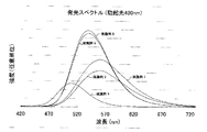
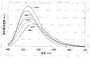
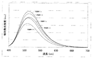
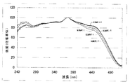
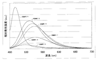
また、図3は、実施例1乃至5のオキシ窒化物蛍光体をEx=400nmで励起したときの発光スペクトルを示す図である。図4は、実施例1乃至5のオキシ窒化物蛍光体をEx=460nmで励起したときの発光スペクトルを示す図である。図5は、実施例1乃至5のオキシ窒化物蛍光体の励起スペクトルを示す図である。図6は、実施例1乃至5のオキシ窒化物蛍光体の反射スペクトルを示す図である。図7は、実施例1のオキシ窒化物蛍光体を撮影したSEM(走査電子顕微鏡)写真である。ここで、色名と色度座標との関係は、JIS Z8110を参酌する。
【0129】
【表1】
実施例1は、CaSi2O2N2:Euである。実施例2は、Ca0.90Mg0.10Si2O2N2:Euである。実施例3は、SrSi2O2N2:Euである。実施例4は、Sr0.90Mg0.10Si2O2N2:Euである。実施例5は、BaSi2O2N2:Euである。
【0131】
まず、原料は、Ca3N2、Si3N4、SiO2、Eu2O3を使用した。該原料を、それぞれ0.1〜3.0μmに粉砕した。粉砕後、実施例1は、下記の数量の原料を使用した。
Ca3N2:6.01g
Si3N4:5.99g
SiO2:7.36g
Eu2O3:0.66g
上記数量を秤量した後、Ca3N2、Si3N4、SiO2、Eu2O3を、窒素雰囲気中、グローブボックス内で、均一になるまで混合した。実施例1乃至5において、Eu濃度は0.43mol%である。
【0132】
実施例1において、原料の混合比率(モル比)は、Ca3N2:Si3N4:SiO2:Eu2O3=1:0.51:3.02:0.046である。この混合比率になるように、Ca3N2(分子量148.3)を6.01g、Si3N4(分子量140.3)を5.99g、SiO2(分子量60.09)を7.36g、Eu2O3(分子量352.0)を0.66gになるように秤量し、混合を行った。
【0133】
上記化合物を混合し、アンモニア雰囲気中で、窒化ホウ素坩堝に投入し、約1500℃で約5時間、焼成を行った。
【0134】
これにより、目的とするオキシ窒化物蛍光体を得た。得られたオキシ窒化物蛍光体の理論組成は、CaSi2O2N2:Euである。
【0135】
実施例1のオキシ窒化物蛍光体のOとNとの重量%を測定すると、全量中にOが19.3重量%、Nが14.5重量%含まれていた。OとNの重量比は、O:N=1:0.75である。
【0136】
実施例に係るオキシ窒化物蛍光体は、窒化ホウ素材質の坩堝を用い、アンモニア雰囲気中で焼成を行っている。坩堝に、金属製の坩堝を使用することはあまり好ましいとはいえない。金属製の坩堝を使用した場合、坩堝が浸食され、発光特性の低下を引き起こすことが考えられるからである。従って、アルミナなどのセラミックス製の坩堝を使用することが好ましい。
【0137】
実施例2は、Caの一部をMgに置換したオキシ窒化物蛍光体である。実施例2は、窒化マグネシウムMg3N2(高純度化学製 98% MGI02PB)(分子量101.0)を用い、原料の混合比率(モル比)が、Ca3N2:Mg3N2:Si3N4:SiO2:Eu2O3=1:0.12:0.57:3.37:0.052となるように、細かく砕いた粉末を、下記の数量、秤量した。
Ca3N2:5.44g
Mg3N2:0.43g
Si3N4:6.05g
SiO2:7.43g
Eu2O3:0.67g
実施例1と同条件で、該原料を混合し、焼成を行った。
【0138】
実施例3は、実施例1のCaをSrに置換したオキシ窒化物蛍光体である。実施例3は、窒化ストロンチウムSr3N4(分子量290.9)を用い、原料の混合比率(モル比)が、Sr3N2:Si3N4:SiO2:Eu2O3=1:0.51:3.02:0.046となるように、細かく砕いた粉末を、下記の数量、秤量した。
Sr3N2:9.14g
Si3N4:4.65g
SiO2:5.71g
Eu2O3:0.51g
実施例3は、実施例1と同条件で、該原料を混合し、焼成を行った。得られた実施例3のオキシ窒化物蛍光体のOとNとの重量%を測定すると、全量中にOが15.3重量%、Nが11.2重量%含まれていた。OとNの重量比は、O:N=1:0.73である。
【0139】
実施例4は、実施例2のCaをSrに置換したオキシ窒化物蛍光体である。実施例4は、原料の混合比率(モル比)が、Sr3N2:Mg3N2:Si3N4:SiO2:Eu2O3=1:0.12:0.57:3.37:0.052となるように、細かく砕いた粉末を、下記の数量、秤量した。
Sr3N2:8.46g
Mg3N2:0.34g
Si3N4:4.80g
SiO2:5.89g
Eu2O3:0.53g
実施例1と同条件で、該原料を混合し、焼成を行った。
【0140】
実施例5は、実施例1のCaをBaに置換したオキシ窒化物蛍光体である。実施例5は、窒化バリウムBa3N2(分子量316.6)を用い、原料の混合比率(モル比)が、Ba3N2:Si3N4:SiO2:Eu2O3=1:0.76:0.22:0.033となるように、細かく砕いた粉末を、下記の数量、秤量した。
Ba3N2:11.2g
Si3N4:3.77g
SiO2:4.63g
Eu2O3:0.42g
実施例1と同条件で、該原料を混合し、焼成を行った。
【0141】
実施例1乃至5の焼成品は、いずれも、結晶性の粉体若しくは粒体である。粒径は、ほぼ1〜5μmであった。
【0142】
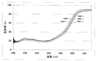
実施例1乃至5のオキシ窒化物蛍光体の励起スペクトルの測定を行った。測定の結果、490nmよりも短波長側で強く励起される。
【0143】
Ex=460nmで実施例1乃至5のオキシ窒化物蛍光体を励起した。Ex=460nmは、青色発光素子でよく使われる波長域であるため、該波長域で励起を行った。その結果、実施例1のオキシ窒化物蛍光体は、色調x=0.437、色調y=0.545の黄緑色領域に発光色を有する。実施例4のオキシ窒化物蛍光体は、色調x=0.351、色調y=0.614の黄緑色領域に発光色を有する。実施例1乃至5のオキシ窒化物蛍光体のいずれも、従来の蛍光体よりも、高い発光効率を示した。
【0144】
Ex=400nmで実施例1乃至5のオキシ窒化物蛍光体を励起した。実施例1のオキシ窒化物蛍光体は、色調x=0.434、色調y=0.543の黄緑色領域に発光色を有する。実施例3のオキシ窒化物蛍光体は、色調x=0.349、色調y=0.608の黄緑色領域に発光色を有する。実施例1乃至5のオキシ窒化物蛍光体のいずれも、従来の蛍光体よりも、高い発光効率を示した。
【0145】
また、温度特性は、極めて良好であった。温度特性は、25℃の発光輝度を100%とする相対輝度で示す。粒径は、F.S.S.S.No.(Fisher Sub Sieve Sizer's No.)という空気透過法による値である。実施例1乃至5の温度特性は、100℃のとき、95〜100%である。200℃のとき、65〜90%であった。
【0146】
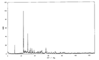
これら上記オキシ窒化物蛍光体のX線回折像を測定したところ、いずれもシャープな回折ピークを示し、得られた蛍光体が、規則性を有する結晶性の化合物であることが明らかとなった。
【0147】
<実施例6乃至15>
表2は、本発明に係るオキシ窒化物蛍光体の実施例6乃至15の特性を示す。
【0148】
また、図8は、実施例6乃至10のオキシ窒化物蛍光体をEx=400nmで励起したときの発光スペクトルを示す図である。図9は、実施例6乃至10のオキシ窒化物蛍光体をEx=460nmで励起したときの発光スペクトルを示す図である。図10は、実施例11乃至15のオキシ窒化物蛍光体をEx=400nmで励起したときの発光スペクトルを示す図である。図11は、実施例11乃至15のオキシ窒化物蛍光体をEx=460nmで励起したときの発光スペクトルを示す図である。図12は、実施例11乃至15のオキシ窒化物蛍光体の励起スペクトルを示す図である。図13は、実施例11乃至15のオキシ窒化物蛍光体の反射スペクトルを示す図である。
【0149】
【表2】
実施例6乃至10は、SrXCa(1−X)Si2O2N2:Eu(0≦X≦1)で表され、SrとCaとのモル比を変えて製造を行っている。
【0151】
実施例6乃至10は、実施例1とほぼ同様の条件でオキシ窒化物蛍光体の製造を行った。原料は、Sr3N2、Ca3N2、Si3N4、SiO2、Eu2O3を使用した。該原料を所定の数量に秤量した後、Sr3N2、Ca3N2、Si3N4、SiO2、Eu2O3を、窒素雰囲気中、グローブボックス内で、均一になるまで混合した。実施例6乃至15において、Eu濃度は0.43mol%である。
【0152】
上記化合物を混合し、アンモニア雰囲気中で、窒化ホウ素坩堝に投入し、約1450℃で約5時間、焼成を行った。
【0153】
これにより、目的とするオキシ窒化物蛍光体が製造された。
【0154】
実施例6乃至10は、発光輝度、量子効率は、実施例6を基準として、相対値で表している。
【0155】
この結果から、400nm近傍の光源で実施例6乃至10を励起させたとき、SrとCaとを混合させたときの方が、Caのみのときよりも、高い発光輝度、量子効率を示した。一方、460nm近傍の光源で実施例6乃至10を励起させたとき、Sr:Ca=7:3のときが、最も発光効率が高かった。また、Caの一部を置換して、Srを増やしていくに従って、発光効率の向上を図ることができる。また、SrとCaのモル比を変えることにより、色調を変化させることが可能である。
【0156】
実施例11乃至15は、SrXCa(10−X)Si2O2N2:Eu(0≦X≦10)で表され、SrとCaとのモル比を変えて製造を行っている。
【0157】
実施例11乃至15は、実施例1とほぼ同様の条件でオキシ窒化物蛍光体の製造を行った。原料は、Sr3N2、Ca3N2、Si3N4、SiO2、Eu2O3を使用した。該原料を所定の数量に秤量した後、Sr3N2、Ca3N2、Si3N4、SiO2、Eu2O3を、窒素雰囲気中、グローブボックス内で、均一になるまで混合した。実施例6乃至15において、Eu濃度は0.43mol%である。
【0158】
上記化合物を混合し、アンモニア雰囲気中で、窒化ホウ素坩堝に投入し、約1550℃で約5時間、焼成を行った。
【0159】
これにより、目的とするオキシ窒化物蛍光体が製造された。
【0160】
実施例11乃至15は、発光輝度、量子効率は、実施例15を基準として、相対値で表している。
【0161】
この結果から、400nm近傍の光源で実施例11乃至15を励起させたとき、SrとCaとを混合させたときの方が、Srのみのときよりも、高い発光輝度、量子効率を示した。また、Sr:Caのモル比が、Sr:Ca=6:4乃至9:1のとき発光効率の向上を図ることができる。特に、Sr:Ca=7:3乃至8:2の時が、発光輝度、量子効率ともに高い値を示している。さらに、SrとCaのモル比を変えることにより、色調を変化させることが可能である。
【0162】
<実施例16乃至20>
表3は、本発明に係るオキシ窒化物蛍光体の実施例10、16乃至20の特性を示す。
【0163】
また、図14は、実施例10、16乃至20のオキシ窒化物蛍光体をEx=400nmで励起したときの発光スペクトルを示す図である。図15は、実施例10、16乃至20のオキシ窒化物蛍光体をEx=460nmで励起したときの発光スペクトルを示す図である。図16は、実施例10、16乃至20のオキシ窒化物蛍光体の励起スペクトルを示す図である。図17は、実施例10、16乃至20のオキシ窒化物蛍光体の反射スペクトルを示す図である。
【0164】
【表3】
実施例10、16乃至20は、SrXBa(1−X)Si2O2N2:Eu(0≦X≦1)で表され、SrとBaとのモル比を変えて製造を行っている。
【0166】
実施例10、16乃至20は、実施例1とほぼ同様の条件でオキシ窒化物蛍光体の製造を行った。原料は、Sr3N2、Ba3N2、Si3N4、SiO2、Eu2O3を使用した。該原料を所定の数量に秤量した後、Sr3N2、Ba3N2、Si3N4、SiO2、Eu2O3を、窒素雰囲気中、グローブボックス内で、均一になるまで混合した。実施例10、16乃至20において、Eu濃度は0.43mol%である。
【0167】
上記化合物を混合し、アンモニア雰囲気中で、窒化ホウ素坩堝に投入し、約1450℃で約5時間、焼成を行った。
【0168】
これにより、目的とするオキシ窒化物蛍光体が製造された。
【0169】
実施例10、16乃至20は、発光輝度、量子効率は、実施例10を基準として、相対値で表している。
【0170】
この結果から、400nm、460nm近傍の光源で実施例10、16乃至20を励起させたとき、Sr:Ba=2:8で混合させたときより、Sr:Ba=6:4乃至8:2で混合させたときの方が、高い発光輝度、量子効率を示した。また、Baの一部を置換して、Srを増やしていくに従って、発光効率の向上を図ることができる。また、SrとCaのモル比を変えることにより、色調を変化させることが可能である。さらに、実施例20のBaSi2N2O2:Euは、496nm近傍に発光ピーク波長を有し、高い発光効率を示す。実施例20に係るオキシ窒化物蛍光体を使用することで、白色系発光装置の演色性の向上を図ることができる。
【0171】
<実施例21乃至24>
表4は、本発明に係るオキシ窒化物蛍光体の実施例21乃至24の特性を示す。
【0172】
また、図18は、実施例21乃至24のオキシ窒化物蛍光体をEx=400nmで励起したときの発光スペクトルを示す図である。図19は、実施例21乃至24のオキシ窒化物蛍光体をEx=460nmで励起したときの発光スペクトルを示す図である。図20は、実施例21乃至24のオキシ窒化物蛍光体の励起スペクトルを示す図である。図21は、実施例21乃至24のオキシ窒化物蛍光体の反射スペクトルを示す図である。
【0173】
【表4】
実施例21乃至24は、CaXBa(1−X)Si2O2N2:Eu(0≦X≦1)で表され、CaとBaとのモル比を変えて製造を行っている。
【0175】
実施例21乃至24は、実施例1とほぼ同様の条件でオキシ窒化物蛍光体の製造を行った。原料は、Ca3N2、Ba3N2、Si3N4、SiO2、Eu2O3を使用した。該原料を所定の数量に秤量した後、Ca3N2、Ba3N2、Si3N4、SiO2、Eu2O3を、窒素雰囲気中、グローブボックス内で、均一になるまで混合した。実施例21乃至24において、Eu濃度は0.43mol%である。
【0176】
上記化合物を混合し、アンモニア雰囲気中で、窒化ホウ素坩堝に投入し、約1450℃で約5時間、焼成を行った。
【0177】
これにより、目的とするオキシ窒化物蛍光体が製造された。
【0178】
実施例21乃至24は、発光輝度、量子効率は、実施例21を基準として、相対値で表している。
【0179】
この結果から、400nm近傍の光源で実施例21乃至24を励起させたとき、Ca:Ba=4:6で混合させたときより、Ca:Ba=8:2で混合させたときの方が、高い発光輝度、量子効率を示した。一方、460nm近傍の光源で実施例21乃至24を励起させたとき、Ca:Ba=2:8で混合させたときより、Ca:Ba=8:2で混合させたときの方が、高い発光輝度、量子効率を示した。また、CaとBaのモル比を変えることにより、色調を変化させることが可能である。
【0180】
<実施例25乃至27>
実施例25乃至27のオキシナイトライド蛍光体について構造解析を行った。実施例25の組成は、CaSi2O2N2である。実施例26の組成は、SrSi2O2N2である。実施例27の組成は、BaSi2O2N2である。図22は、斜方晶系を示す概略図である。図23は、実施例25のオキシナイトライド蛍光体のX線回折パターンを示す図である。図24は、実施例26のオキシナイトライド蛍光体のX線回折パターンを示す図である。図25は、実施例27のオキシナイトライド蛍光体のX線回折パターンを示す図である。
【0181】
この結果から、シリコンナイトライド系蛍光体の結晶の単位格子は、斜方晶系に帰属される。斜方晶系は、a≠b≠c、α=β=γ=90°であり、互いに垂直な2回対称軸三つ、あるいは2回対称軸と交わる二つの対称面を有する。
【0182】
<発光装置>
上述のオキシ窒化物蛍光体を用いて、実施例1の発光装置を製造した。励起光源として、400nmの発光スペクトルを有する発光素子を使用する。蛍光体は、実施例1のCaSi2O2N2:Euと、Ca2Si5N8:Euと、(Ca0.93,Eu0.05,Mn0.02)10(PO4)6Cl2を使用する。図1は、本発明に係る発光装置を示す。図26は、本発明に係る発光素子を示す平面図である。図27は、本発明に係る発光素子のA−A‘を示す断面図である。図28は、実施例1の発光装置の発光スペクトルを示す図である。図29は、本発明に係る実施例1の発光装置の色度座標を示す図である。
【0183】
(発光素子)
サファイア(C面)よりなる基板201をMOVPEの反応容器内にセットし、水素を流しながら、基板201の温度を約1050℃まで上昇させ、基板201のクリーニングを行う。
【0184】
ここで、本実施例では、基板201に、サファイア基板を用いているが、基板201として窒化物半導体と異なる異種基板、AlN、AlGaN、GaN等の窒化物半導体基板を用いてもよい。異種基板としては、例えば、C面、R面及びA面のいずれかを主面とするサファイア、スピネル(MgAl2O4のような絶縁性基板、SiC(6H、4H、3Cを含む)、ZnS、ZnO、GaAs、Si及び窒化物半導体と格子整合する酸化物基板等、窒化物半導体を成長させることが可能であり、窒化物半導体と異なる基板材料を用いることができる。好ましい異種基板としては、サファイア、スピネルが挙げられる。また、異種基板は、オフアングルしていてもよく、この場合、ステップ状にオフアングルしたものを用いると窒化ガリウムからなる下地層202の成長が結晶性よく成長するため好ましい。更に、異種基板を用いる場合には、異種基板上に素子構造形成前の下地層202となる窒化物半導体を成長させた後、異種基板を研磨などの方法により除去して、窒化物半導体の単体基板として素子構造を形成してもよく、また、素子構造形成後に、異種基板を除去する方法でも良い。GaN基板の他に、AlN等の窒化物半導体の基板を用いても良い。
【0185】
(バッファ層)
続いて、基板201の温度を510℃まで下げ、キャリアガスに水素、原料ガスにアンモニアとTMG(トリメチルガリウム)とを用い、基板201上にGaNよりなるバッファ層(図示しない)を約100オングストロームの膜厚で成長させる。
【0186】
(下地層)
バッファ層成長後、TMGのみ止めて、基板201の温度を1050℃まで上昇させる。1050℃になったら、同じく原料ガスにTMG、アンモニアガスを用い、アンドープGaN層を2μmの膜厚で成長させる。
【0187】
(n型層)
続いて1050℃で、同じく原料ガスにTMG、アンモニアガス、不純物ガスにシランガスを用い、Siを4.5×10¹⁸/cm3ドープしたGaNよりなるn型層203を、n型層としてn側電極211aを形成するn側コンタクト層として、厚さ3μmで成長させる。
【0188】
(活性層)
SiドープGaNよりなる障壁層を50オングストロームの膜厚で成長させ、続いて温度を800℃にして、TMG、TMI、アンモニアを用いアンドープIn0.1Ga0.7Nよりなる井戸層を50オングストロームの膜厚で成長させる。そして障壁+井戸+障壁+井戸・・・+障壁の順で障壁層を4層、井戸を3層、交互に積層して、総膜厚350オングストロームの多重量子井戸構造よりなる活性層204を成長させる。
【0189】
(p側キャリア閉込め層)
次に、TMG、TMA、アンモニア、Cp2Mg(シクロペンタジエニルマグネシウム)を用い、Mgを5×10¹⁹/cm3ドープしたAl0.3Ga0.7Nよりなるp側キャリア閉込め層205を、膜厚100オングストロームで成長させる。
【0190】
(第1p型層)
続いて、TMG、アンモニア、Cp2Mgを用い、p型不純物をドープしたGaNよりなる第1p型層206を、膜厚0.1μmで成長させる。
【0191】
(第2p型層)
第2p型層として、表面にp側電極210を形成するp側コンタクト層208を形成する。p側コンタクト層208は、電流拡散層207の上に、Mgを1×10²⁰/cm3ドープしたp型GaNを150オングストロームの膜厚で成長させる。p側コンタクト層208は、p側電極210を形成する層であるので、1×1017/cm3以上の高キャリア濃度とすることが望ましい。1×1017/cm3よりも低いと電極と好ましいオーミックを得るのが難しくなる傾向にある。さらにコンタクト層の組成をGaNとすると、電極材料と好ましいオーミックが得られやすくなる。
【0192】
以上の素子構造を形成する反応を終了した後、温度を室温まで下げ、さらに窒素雰囲気中、ウェハーを反応容器内において、700℃でアニーリングを行い、p型層をさらに低抵抗化する。素子構造を形成したウェハーを装置から取り出し、以下に説明する電極形成工程を実施する。
【0193】
アニーリング後、ウェハーを反応容器から取り出し、最上層のp側コンタクト層208の表面に所定のマスクを形成し、RIE(反応性イオンエッチング)装置でp側コンタクト層208側からエッチングを行い、n側コンタクト層の表面を露出させて、電極形成面を形成する。
【0194】
p側電極210として、Ni、Auを順に積層して、Ni/Auよりなるp側電極210を形成する。また、このp側電極210は、第2p型層、p側コンタクト層208にオーミック接触させたオーミック電極となる。このとき、形成された電極枝210aは、ストライプ状の発光部209の幅を約5μm、ストライプ状の電極枝210aの幅を約3μmとし、ストライプ状の発光部209と電極枝210aを交互に形成する。また、p側パット電極が形成される領域には、p側電極210を一部だけ形成し、p側パット電極の上にわたって形成して、電気的に導通させる。このとき、p側パット電極が形成される領域には、p側電極210を一部だけ形成し、p側パット電極210bを、p側コンタクト層208の表面上に形成して、一部をp側電極210の上にわたって形成して、電気的に導通させる。このとき、p側パット電極210bが設けられるp側コンタクト層208の表面は、p側電極210とp側コンタクト層208とはオーミック接触させずに、ショットキー障壁が両者の間に形成されて、p側パット電極210bの形成部からは、直接素子内部に電流が流れずに、電気的に接続された電極枝210aを通って、電流を素子内部に注入する構造となる。
【0195】
続いて、n型層203を露出させた露出面203aに、n側電極211aを形成する。n側電極211aは、Ti、Alを積層して形成する。
【0196】
ここで、n側電極211aは、n型層203の露出面203aにオーミック接触させたオーミック電極となる。オーミック用のp側電極210、n側電極211aを形成した後、熱処理でアニールして、各電極をオーミック接触させる。この時得られるp側のオーミック電極は、活性層204の発光をほぼ透過しない不透光性膜となる。
【0197】
続いて、上記p側電極210、n側電極211aの一部、若しくは全部を除く表面全体に、すなわち、n型層203の露出面203a及び該露出面203aの側面などの素子表面全体に、SiO2よりなる絶縁膜を形成する。絶縁膜形成後、絶縁膜から露出したp側電極210、n側電極211aの表面に、それぞれボンディング用のパット電極を形成して、各オーミック用の電極に電気的に導通させる。p側パット電極210b、n側パット電極211bは、各オーミック用の電極の上に、Ni、Ti、Auを積層してそれぞれ形成する。
【0198】
最後に、基板201を分割して、一辺の長さが300μmの発光素子を得る。
【0199】
得られた発光素子は、発光ピーク波長が約400nmである。
【0200】
実施例1の発光装置の特性を表5に示す。
【0201】
【表5】
これより、実施例1の発光装置は、白色域に発光色を示す。実施例1の発光装置は、360〜430nm、430〜500nm、500〜730nmに発光ピーク波長がある発光スペクトルを示している。より具体的には、390〜410nm、455〜475nm、550〜600nmに発光ピーク波長がある発光スペクトルを示す。400nm励起の発光素子により励起された蛍光体は、実施例1のCaSi2O2N2:Euは、緑色系領域に、Ca2Si5N8:Euは、黄色から赤色系領域に、(Ca0.93,Eu0.05,Mn0.02)10(PO4)6Cl2は、青色系領域に、それぞれ発光ピーク波長を有する。これらの蛍光体の光の混色により、白色系領域に発光色を示す。これらの蛍光体の配合量を変更することにより、種々の色味の白色光を発する。従って、励起光源として、紫外光を用いて所定の白色光を有する発光装置を製造する場合、蛍光体の種類、配合比等を変更するだけで、発光色を変更することができる。
【0203】
<発光装置>
実施例2の発光装置は、励起光源に発光ピーク波長が460nmの発光素子を用いた白色発光装置に関する。図1は、本発明に係る発光装置を示す図である。
【0204】
実施例2の発光装置は、サファイア基板1上にn型及びp型のGaN層の半導体層2が形成され、該n型及びp型の半導体層2に電極3が設けられ、該電極3は、導電性ワイヤ14によりリードフレーム13と導電接続されている。発光素子10の上部は、蛍光体11及びコーティング部材12で覆われ、リードフレーム13、蛍光体11及びコーティング部材12等の外周をモールド部材15で覆っている。半導体層2は、サファイア基板1上にn+GaN:Si、n−AlGaN:Si、n−GaN、GaInN QWs、p−GaN:Mg、p−AlGaN:Mg、p−GaN:Mgの順に積層されている。該n+GaN:Si層の一部はエッチングされてn型電極が形成されている。該p−GaN:Mg層上には、p型電極が形成されている。リードフレーム13は、鉄入り銅を用いる。マウントリード13aの上部には、発光素子10を積載するためのカップが設けられており、該カップのほぼ中央部の底面に該発光素子10がダイボンドされている。導電性ワイヤ14には、金を用い、電極3と導電性ワイヤ14を導電接続するためのバンプ4には、Niメッキを施す。蛍光体11には、実施例49の蛍光体とYAG系蛍光体とを混合する。コーティング部材12には、エポキシ樹脂と拡散剤、チタン酸バリウム、酸化チタン及び前記蛍光体11を所定の割合で混合したものを用いる。モールド部材15は、エポキシ樹脂を用いる。この砲弾型の発光装置1は、モールド部材15の半径2〜4mm、高さ約7〜10mmの上部が半球の円筒型である。
【0205】
実施例2の発光装置に電流を流すと、ほぼ460nmに発光ピーク波長がある青色発光素子10が発光する。この青色光を、半導体層2を覆う蛍光体11が色調変換を行う。その結果、白色に発光する実施例2の発光装置を提供することができる。
【0206】
本発明に係る実施例2の発光装置の蛍光体11は、実施例1のオキシ窒化物蛍光体と、CaSrSi5N8:Euで表される窒化物蛍光体と、を混合した蛍光体11を用いる。該蛍光体11は、コーティング部材12と一緒に混合されている。
【0207】
実施例2の発光装置は、発光素子10の光の一部が透過する。また、発光素子10の光の一部が蛍光体11を励起し、該蛍光体11は、波長変換を行い、オキシ窒化物蛍光体の緑色と、窒化物蛍光体の黄赤から赤色との光を発する。これらの発光素子10からの青色光と、オキシ窒化物蛍光体からの緑色光と、窒化物蛍光体の黄赤から赤色光と、の光の混色により、白色に発光する発光装置を提供することができる。
【0208】
<発光装置>
図30は、本発明に係るキャップタイプの発光装置を示す図である。
【0209】
実施例3の発光装置は、実施例1の発光装置における部材と同一の部材には同一の符号を付して、その説明を省略する。発光素子10は、400nmに発光ピーク波長を有する発光素子を使用する。
【0210】
実施例3の発光装置は、実施例1の発光装置のモールド部材15の表面に、蛍光体(図示しない)を分散させた光透過性樹脂からなるキャップ16を被せることにより構成される。
【0211】
マウントリード13aの上部に、発光素子10を積載するためのカップが設けられており、該カップのほぼ中央部の底面に該発光素子10がダイボンドされている。実施例1の発光装置では、該カップの上部に発光素子10を覆うように、蛍光体11が設けられているが、実施例3の発光装置では、特に設けなくてもよい。該発光素子10の上部に蛍光体11を設けないことにより、発光素子10から発生する熱の影響を直接受けないからである。
【0212】
キャップ16は、蛍光体を光透過性樹脂に均一に分散させている。この蛍光体を含有する光透過性樹脂を、発光装置1のモールド部材15の形状に嵌合する形状に成形している。または、所定の型枠内に蛍光体を含有する光透過性樹脂を入れた後、発光装置1を該型枠内に押し込み、成型する製造方法も可能である。キャップ16の光透過性樹脂の具体的材料としては、エポキシ樹脂、ユリア樹脂、シリコーン樹脂などの温度特性、耐候性に優れた透明樹脂、シリカゾル、ガラス、無機バインダーなどが用いられる。上記の他、メラミン樹脂、フェノール樹脂等の熱硬化性樹脂を使用することができる。また、ポリエチレン、ポリプロピレン、ポリ塩化ビニル、ポリスチレン等の熱可塑性樹脂、スチレン−ブタジエンブロック共重合体、セグメント化ポリウレタン等の熱可塑性ゴム等も使用することができる。また、蛍光体と共に拡散剤、チタン酸バリウム、酸化チタン、酸化アルミニウムなどを含有させても良い。また、光安定化剤や着色剤を含有させても良い。キャップ16に使用される蛍光体は、Ca2Si5N8:Euの窒化物蛍光体と、(Ca0.95,Eu0.05)10(PO4)6Cl2の蛍光体とを使用する。マウントリード13aのカップ内に用いられる蛍光体11は、実施例3のオキシ窒化物蛍光体を用いる。しかし、キャップ16に蛍光体を用いるため、オキシ窒化物蛍光体をキャップ16に含有し、マウントリード13aのカップ内は、コーティング部材12のみでもよい。
【0213】
このように構成された発光装置は、発光素子10から放出される光の一部は、蛍光体11のオキシ窒化物蛍光体を励起し、緑色に発光する。また、発光素子10から放出される光の一部、若しくはオキシ窒化物蛍光体から放出される光の一部がキャップ16の蛍光体を励起し、青色と黄色から赤色に発光する。これにより、オキシ窒化物蛍光体の緑色光と、キャップ16の蛍光体の青色と黄色から赤色光とが混合し、結果として、キャップ16の表面からは、白色系の光が外部へ放出される。
【0214】
【発明の効果】
以上のことから、本発明は、近紫外から可視光の短波長側領域の励起光源と、該励起光源からの光により励起される、緑色から黄色系領域に発光色を示す蛍光体と、を少なくとも有する発光装置である。該発光装置は、鮮やかな発光色を示す。特に、紫外光を有する発光素子からの光により、オキシ窒化物蛍光体は、緑色から黄色系領域の発光色を示す。また、オキシ窒化物蛍光体の組成比を変えることにより、発光特性に優れた発光装置を提供することができる。また、発光効率の高い、再現性に優れた発光装置である。従って、本発明は、上述のような発光装置を提供することができるという極めて重要な技術的意義を有する。
【図面の簡単な説明】
【図1】 本発明に係る砲弾型の発光装置1を示す図である。
【図2】 (a)本発明に係る表面実装型の発光装置を示す平面図である。(b)本発明に係る表面実装型の発光装置の断面図である。
【図3】 実施例1乃至5のオキシ窒化物蛍光体をEx=400nmで励起したときの発光スペクトルを示す図である。
【図4】 実施例1乃至5のオキシ窒化物蛍光体をEx=460nmで励起したときの発光スペクトルを示す図である。
【図5】 実施例1乃至5のオキシ窒化物蛍光体の励起スペクトルを示す図である。
【図6】 実施例1乃至5のオキシ窒化物蛍光体の反射スペクトルを示す図である。
【図7】 実施例1のオキシ窒化物蛍光体を撮影したSEM写真である。
【図8】 実施例6乃至10のオキシ窒化物蛍光体をEx=400nmで励起したときの発光スペクトルを示す図である。
【図9】 実施例6乃至10のオキシ窒化物蛍光体をEx=460nmで励起したときの発光スペクトルを示す図である。
【図10】 実施例11乃至15のオキシ窒化物蛍光体をEx=400nmで励起したときの発光スペクトルを示す図である。
【図11】 実施例11乃至15のオキシ窒化物蛍光体をEx=460nmで励起したときの発光スペクトルを示す図である。
【図12】 実施例11乃至15のオキシ窒化物蛍光体の励起スペクトルを示す図である。
【図13】 実施例11乃至15のオキシ窒化物蛍光体の反射スペクトルを示す図である。
【図14】 実施例10、16乃至20のオキシ窒化物蛍光体をEx=400nmで励起したときの発光スペクトルを示す図である。
【図15】 実施例10、16乃至20のオキシ窒化物蛍光体をEx=460nmで励起したときの発光スペクトルを示す図である。
【図16】 実施例10、16乃至20のオキシ窒化物蛍光体の励起スペクトルを示す図である。
【図17】 実施例10、16乃至20のオキシ窒化物蛍光体の反射スペクトルを示す図である。
【図18】 実施例21乃至24のオキシ窒化物蛍光体をEx=400nmで励起したときの発光スペクトルを示す図である。
【図19】 実施例21乃至24のオキシ窒化物蛍光体をEx=460nmで励起したときの発光スペクトルを示す図である。
【図20】 実施例21乃至24のオキシ窒化物蛍光体の励起スペクトルを示す図である。
【図21】 実施例21乃至24のオキシ窒化物蛍光体の反射スペクトルを示す図である。
【図22】 斜方晶系を示す概略図である。
【図23】 実施例25のオキシナイトライド蛍光体のX線回折パターンを示す図である。
【図24】 実施例26のオキシナイトライド蛍光体のX線回折パターンを示す図である。
【図25】 実施例27のオキシナイトライド蛍光体のX線回折パターンを示す図である。
【図26】 本発明に係る発光素子を示す平面図である。
【図27】 本発明に係る発光素子のA−A‘を示す断面図である。
【図28】 本発明に係る実施例1の発光装置の発光スペクトルを示す図である。
【図29】 本発明に係る実施例1の発光装置の色度座標を示す図である。
【図30】 本発明に係るキャップタイプの発光装置3を示す図である。
【符号の説明】
1 基板
2 半導体層
3 電極
4 バンプ
10 発光素子
11 蛍光体
12 コーティング部材
13 リードフレーム
13a マウントリード
13b インナーリード
14 導電性ワイヤ
15 モールド部材
101 発光素子
102 リード電極
103 絶縁封止材
104 導電性ワイヤ
105 パッケージ
106 リッド
107 窓部
108 蛍光体
109 コーティング部材
201 基板
202 下地層
203 n型層
203a 露出面
204 活性層
205 p側キャリア閉込め層
206 第1p型層
207 電流拡散層
208 p側コンタクト層
209 発光部
210 p側電極
210a 電極枝
210b p側パット電極
211a n側電極
211b n側パット電極[0001]
BACKGROUND OF THE INVENTION
The present invention relates to a phosphor that emits light by being excited by electromagnetic waves such as light, electron beams, and X-rays, heat, and the like. . In particular, the present invention relates to white and multicolor light emitting devices using semiconductor light emitting elements.
[0002]
[Prior art]
A light-emitting device using a light-emitting element emits light of a bright color that is small and power efficient. In addition, since the light-emitting element is a semiconductor element, there is no fear of a broken ball. Further, it has excellent initial driving characteristics and is strong against vibration and repeated on / off lighting. Because of such excellent characteristics, light emitting devices using semiconductor light emitting elements such as LEDs and LDs are used as various light sources.
[0003]
A part or all of the light of the light emitting element is converted in wavelength by a phosphor, and the emission color different from the light of the light emitting element is emitted by mixing and emitting the wavelength converted light and the light of the light emitting element that is not wavelength converted. Light emitting devices that emit light have been developed.
[0004]
Among these light emitting devices, white light emitting devices are required in a wide range of fields such as lighting such as fluorescent lamps, in-vehicle lighting, displays, and backlights for liquid crystals. In addition, there are demands for light emitting devices of various colors such as pastel colors by combining a semiconductor light emitting element and a phosphor.
[0005]
The emission color of a light emitting device using a white semiconductor light emitting element is obtained by the principle of light color mixing. The blue light emitted from the light emitting element enters the phosphor layer, and after being repeatedly absorbed and scattered several times in the layer, is emitted to the outside. On the other hand, the blue light absorbed by the phosphor serves as an excitation light source and emits yellow fluorescence. This yellow light and blue light are mixed and appear as white to the human eye.
[0006]
For example, a blue light emitting element is used as the light emitting element, and a phosphor is thinly coded on the surface of the blue light emitting element. The light emitting element is a blue light emitting element using an InGaN-based material. The phosphor is (Y, Gd)3(Al, Ga)5O12: YAG phosphor represented by the composition formula of Ce is used.
[0007]
In recent years, a white light emitting device using a light emitting element in the short wavelength side region of visible light and combining a phosphor emitting blue light and a YAG phosphor emitting yellow light has been reported. In this case, the YAG phosphor that emits yellow light is hardly excited by light in the short wavelength side region of visible light and does not emit light. For this reason, the blue phosphor is excited by the light emitting element to emit blue light. Next, the YAG phosphor is excited by the blue light and emits yellow light. Thus, white light is emitted by mixing the blue light of the blue phosphor and the yellow light of the YAG phosphor.
[0008]
Various phosphors have been developed for use in the light emitting device.
[0009]
For example, oxide phosphors using rare earth elements as the emission center have been widely known and some of them have been put into practical use. However, nitride phosphors and oxynitride phosphors have not been studied much, and only a few research reports have been made compared to oxide phosphors. For example, there is an oxynitride glass phosphor represented by Si—O—N, Mg—Si—O—N, Ca—Al—Si—O—N, or the like (see Patent Document 1). Further, there is an oxynitride glass phosphor represented by Ca—Al—Si—O—N activated with Eu (see Patent Document 2).
[0010]
[Patent Document 1]
JP 2001-214162 A
[Patent Document 2]
JP 2002-76434 A
[0011]
[Problems to be solved by the invention]
However, conventional phosphors have low emission luminance and are insufficient for use in light emitting devices. In a light emitting device using a light emitting element in the near-ultraviolet region, etc. as an excitation light source, the blue phosphor is excited by the light emitting element, and the YAG phosphor is excited by the excitation light. It is difficult to obtain white light. Therefore, there is a demand for a phosphor that is directly wavelength-converted by light in the short wavelength side region of visible light and emits green to yellow.
[0012]
In addition, as for a white light emitting device using a light emitting element in the short wavelength side region of visible light and a phosphor, an appropriate phosphor is not manufactured, and a light emitting device that can withstand practical use is not commercially available. Therefore, there is a demand for a phosphor that efficiently emits light in the short wavelength region of visible light.
[0013]
In addition, the oxynitride phosphors and the like disclosed in
[0014]
Accordingly, an object of the present invention is to provide a light emitting device using a phosphor having a light emission color from green to yellow that is excited by an excitation light source in the near ultraviolet to visible light region and wavelength-converted. It is another object of the present invention to provide a light emitting device with high luminous efficiency and excellent reproducibility.
[0015]
[Means for Solving the Problems]
In order to solve the above-described problems, the present invention provides a light-emitting device that includes an excitation light source and a phosphor that converts the wavelength of at least part of light from the excitation light source. There is an emission peak wavelength in the red region, and it contains an oxynitride phosphor with crystals. The oxynitride phosphor has the general formula Sr x Ca 1-x Si 2 O 2 N 2 : Eu (0.3 ≦ x ≦ 0.7) and CaSi 2 O 2 N 2 : Oxynitride phosphor having an emission peak wavelength shorter than Eu. Alternatively, the oxynitride phosphor is of the general formula Ca x Ba 1-x Si 2 O 2 N 2 : Represented by Eu (0.2 ≦ x ≦ 0.4)The present invention relates to a light emitting device. Thus, a light emitting device with high light emission efficiency can be provided. A yellow-based YAG-based phosphor having a light emission peak wavelength emits little light even when excited using non-myopic excitation light, but the oxynitride phosphor according to the present invention has a short wavelength from ultraviolet to visible light. It emits light by the excitation light in the side region and exhibits high luminous efficiency.
[0016]
Here, the short wavelength side region from ultraviolet to visible light is not particularly limited, but refers to a region of 240 to 500 nm or less. In particular, a range of 290 to 470 nm is preferable. More preferably, it is the range of 340-410 nm.
[0017]
The blue-green to yellow-red system region conforms to JIS Z8110. Specifically, the blue-green to yellow-red region refers to a range of 485 to 610 nm.
[0018]
The oxynitride phosphor is, BeAnd at least one selected from the group consisting of C, Si, Ge, Sn, Ti, Zr, and Hf, and at least one group II element selected from the group consisting of Mg, Ca, Sr, Ba, and Zn A group IV element as described above;It consists of a crystal containing a rare earth element as activator R, and has an orthorhombic unit cellAn oxynitride phosphor is preferable. The oxynitride phosphor containing the above elements is excited by an excitation light source in the short wavelength side region of near ultraviolet to visible light, and absorbs a part of the light of the excitation light source. The excited and absorbed oxynitride phosphor performs wavelength conversion. The wavelength-converted light has an emission peak wavelength from green to yellow. As a result, the oxynitride phosphor absorbs part of the light from the light emitting element and has an emission spectrum having an emission peak wavelength in the green to yellow range. In addition, the oxynitride phosphor has high light emission efficiency, and can emit light from the light emitting element very efficiently. Furthermore, it is possible to provide a light emitting device that emits an intermediate color from the light emission color of the light emitting element to the light emission color of the oxynitride phosphor by mixing colors of light from the light emitting element and light of the oxynitride phosphor.
[0019]
The oxynitride phosphor preferably contains O and N in the composition, and the weight ratio of O to N is 1 to 0, and N is preferably 0.2 to 2.1. The molar ratio oxynitride phosphor is excited by light such as near ultraviolet, has a light emission peak wavelength from green to yellow, and exhibits high light emission efficiency.
[0020]
The oxynitride phosphor has a general formula: LXMYOZN((2/3) X + (4/3) Y- (2/3) Z): R or LXMYQTOZN((2/3) X + (4/3) Y + T- (2/3) Z): R (L is a Group II element that is at least one selected from the group consisting of Be, Mg, Ca, Sr, Ba, Zn. M is C, Si, Ge, Sn, Ti, Zr. , Hf is at least one group IV element selected from the group consisting of Hf, and Q is at least one group III element selected from the group consisting of B, Al, Ga, In. O is an oxygen element, N is a nitrogen element, R is a rare earth element, 0.5 <X <1.5, 1.5 <Y <2.5, 0 <T <0. 5, 1.5 <Z <2.5). The oxynitride phosphor is excited by excitation light in the short wavelength region from near ultraviolet to visible light, and has an emission peak wavelength from green to yellow. Further, the oxynitride phosphor has equal or higher stability than the YAG phosphor. Furthermore, since the oxynitride phosphor is not a glass body (amorphous) and the light emitting part is a crystalline powder or granule, it is easy to manufacture and process. By setting the X, Y, T, and Z within the above ranges, a phosphor with good luminous efficiency can be provided. That is, within the above range, a crystal layer having substantially light emitting properties is formed. On the other hand, when it is out of the above range, the light emission efficiency is lowered.
[0021]
X, Y, and Z are preferably X = 1, Y = 2, and Z = 2. This is because at the time of the composition, crystallinity is improved and luminous efficiency is increased.
[0022]
70% by weight or more of R is preferably Eu. The rare earth element R is preferably Eu since it has high luminous efficiency. This is because high luminous efficiency can be obtained by using the Eu amount within this range.
[0023]
The oxynitride phosphor relates to an oxynitride phosphor characterized in that at least a part thereof has a crystal. Particularly preferably, the oxynitride phosphor has at least 50% by weight, more preferably 80% by weight or more of crystals. This indicates the ratio of the crystal phase having luminescence, and it is preferable to have 50% by weight or more of the crystal phase because light emission that can withstand practical use can be obtained. Therefore, the more crystal phases, the better. Thereby, the light emission luminance can be increased, and the manufacture and processing of the oxynitride phosphor can be facilitated.
[0024]
The crystal has an orthorhombic unit cell. When the crystal structure is analyzed from the X-ray diffraction pattern of the phosphor, the unit cell of the crystal belongs to the orthorhombic system.
[0025]
The oxynitride phosphor preferably has an excitation spectrum having a higher intensity at 370 nm than at 500 nm. Thereby, the ultraviolet region shows higher luminance than the blue region. That is, higher light emission efficiency can be exhibited by using the light emitting element in the ultraviolet region than using the light emitting element in the blue region.
[0026]
The oxynitride phosphor preferably has a certain Group II element selected from the group consisting of at least two types of Be, Mg, Ca, Sr, Ba, and Zn. This is because light emission characteristics such as color tone, light emission luminance, and quantum efficiency can be changed.
[0027]
The oxynitride phosphor has Sr and Ca, and the molar ratio of Sr and Ca is larger than Sr: Ca = 0: 10 and smaller than 10: 0, more preferably 3: 7. It is preferably from 9: 1. The oxynitride phosphor has Sr and Ba, and the molar ratio of Sr and Ba is Sr: Ba = 5: 5 or more and smaller than 10: 0, more preferably 6: 4. It is preferably from 9: 1. The oxynitride phosphor has Ca and Ba, and the molar ratio of Ca to Ba is larger than Ca: Ba = 0: 10 and smaller than 10: 0, more preferably 1. : 9 to 9: 1 is preferable. Oxynitride phosphors of various colors can be manufactured by a predetermined combination. In addition, by setting this range, it is possible to improve the light emission efficiency.
[0028]
The excitation light source relates to a light emitting device having at least one emission peak wavelength in a short wavelength side region from ultraviolet to visible light. This is because a phosphor with high luminous efficiency can be provided by using an excitation light source in this range. In particular, it is preferable to use an excitation light source having an emission peak wavelength at 240 to 470 nm, and it is preferable to use an excitation light source having an emission peak wavelength at 350 to 410 nm.
[0029]
The excitation light source is preferably a light emitting element. The light emitting element is small in size, has high power efficiency, and emits bright colors. In addition, since the light-emitting element is a semiconductor element, there is no fear of a broken ball. Further, it has excellent initial driving characteristics and is strong against vibration and repeated on / off lighting. Therefore, a light-emitting device that combines a light-emitting element and an oxynitride phosphor is preferable.
[0030]
The light emitting layer of the light emitting element preferably includes a nitride semiconductor containing In. Thereby, the light emitting element emits light having an emission peak wavelength in the vicinity of 350 to 410 nm, and the oxynitride phosphor is excited by the light from the light emitting element, and exhibits a predetermined emission color. This is because the oxynitride phosphor strongly emits light in the vicinity of 350 to 410 nm, and thus a light emitting element in this wavelength region is required. In addition, since the emission spectrum width can be narrowed, the oxynitride phosphor can be excited efficiently, and the emission spectrum that does not substantially affect the color tone change from the light emitting device. Can be released.
[0031]
The phosphor includes a second phosphor used together with the oxynitride phosphor, and the second phosphor includes light from the excitation light source and light from the oxynitride phosphor. The present invention relates to a light-emitting device characterized in that at least a part of is converted into a wavelength and has an emission peak wavelength in the visible light region. Thus, a light emitting device having a light emission color in the visible light region can be provided by mixing the light from the excitation light source, the light of the oxynitride phosphor, and the light of the second phosphor. The light emitting device can emit a desired light emission color in a wavelength range from the emission color of the excitation light source to the emission color of the oxynitride phosphor or the emission color of the second phosphor.
[0032]
The second phosphor relates to a light emitting device having at least one emission peak wavelength from a blue region to a green, yellow, and red region. This is because the light emitting device can exhibit a desired emission color. In particular, by combining the three primary colors of the green color of the oxynitride phosphor excited by an excitation light source having an emission peak wavelength in the short wavelength region from ultraviolet to visible light, the blue color of the second phosphor, and the red color, This is because various emission colors can be realized. However, the light emitting device may be a combination of two kinds of colors such as green and red and green and yellow.
[0033]
The second phosphors are alkaline earth halogen apatite phosphors, alkaline earth metal borate phosphors, alkaline earths mainly activated by lanthanoids such as Eu and transition metal elements such as Mn. Mainly activated by lanthanoid elements such as metal aluminate phosphors, alkaline earth silicates, alkaline earth sulfides, alkaline earth thiogallate, alkaline earth silicon nitride, germanate, or Ce It is preferably at least one selected from a rare earth aluminate, a rare earth silicate, or an organic or organic complex mainly activated by a lanthanoid element such as Eu. This is because it is possible to provide a light emitting device having high light emission efficiency such as light emission luminance and quantum efficiency. In addition, a light-emitting device with favorable color rendering properties can be provided. However, the second phosphor is not limited to the above, and phosphors that emit light in various colors can be used.
[0034]
The light emitting device emits a mixture of at least two of the light from the excitation light source, the light from the oxynitride phosphor, and the light from the second phosphor. It is preferred that Thereby, the emission color of the light emitting device can be adjusted, and a desired emission color can be emitted. In particular, when a light emitting element that emits light in the ultraviolet region is used, the human eye can hardly see the emission color in the ultraviolet region. Therefore, the color of light emitted by mixing the light from the oxynitride phosphor and the light from the second phosphor is shown. Since the luminescent color is determined only by the phosphor, the luminescent color can be easily adjusted. Here, although expressed as the second phosphor, the second phosphor is not limited to one type, and several types of phosphors may be included. This is because by including several kinds of phosphors, more delicate chromaticity adjustment is possible. In particular, when a light-emitting element having a short wavelength region such as ultraviolet light or visible light is used, light from the light-emitting element is less likely to be perceived by human eyes, and thus there is little chromaticity shift due to manufacturing variations.
[0035]
The light emitting device may have an intermediate emission color from an emission peak wavelength of the excitation light source to an emission peak wavelength of the oxynitride phosphor or an emission peak wavelength of the second phosphor. The emission spectrum of the excitation light source is on the shorter wavelength side than the oxynitride phosphor or the second phosphor, and has high energy. The emission color from this high energy region to the low energy region of the oxynitride phosphor and the second phosphor can be emitted. In particular, the emission color from the emission peak wavelength of the light emitting element to the first emission peak wavelength of the oxynitride phosphor or the second emission peak wavelength of the second phosphor is shown. For example, when the emission peak wavelength of the light emitting element is in the blue region, the emission peak wavelength of the excited first phosphor is green, and the emission peak wavelength of the excited second phosphor is red, 3 It is possible to show a white emission color by mixing colors. As a different example, the emission peak wavelength of the light emitting element is in the ultraviolet region, the emission peak wavelength of the excited first phosphor is green, and the emission peak wavelength of the excited second phosphor is yellow and red. In some cases, it is possible to show slightly yellowish white and multicolored emission colors. By changing the blending amount of the oxynitride phosphor and the second phosphor, light emission from a color close to the emission color of the oxynitride phosphor to a color close to the emission color of the second phosphor Can show the color. Further, when the second phosphor has two or more emission peak wavelengths, the emission peak wavelength of the excitation light source, the emission peak wavelength of the oxynitride phosphor, and two or more of the second phosphor have It is a light-emitting device which shows the luminescent color between the light emission peak wavelengths. The second phosphor can be used not only in one type but also in combination of two or more types. In addition to light emitting devices that emit white light, there is also a need for light emitting devices that emit light in various colors such as pastel colors. A light-emitting device having a desired color can be provided by variously combining a green-based oxynitride phosphor, a red-based phosphor, and a blue-based phosphor. Light emitting devices with different colors are not only a method of changing the type of phosphor, but also a method of changing the blending ratio of the phosphors to be combined, a method of changing the coating method of applying the phosphor to the excitation light source, There is a method to adjust the lighting time of.
[0036]
The intermediate emission color preferably emits white light. In particular, it is preferable to emit white light near the locus of blackbody radiation. This is because it can be used for various purposes such as illumination, a liquid crystal backlight, and a display.
[0037]
The light-emitting device is preferably a light-emitting device having an emission spectrum having at least one emission peak wavelength at 430 to 500 nm and 500 to 730 nm. A light emitting device that emits light in a desired color can be provided by combining blue light, green light, red light, and the like. For this reason, color rendering properties can be improved by combining several phosphors. Even with the same white light emission, there are whites that are yellowish and whites that are bluish. Therefore, it has an emission spectrum with an emission peak wavelength in the above range.
As described above, the light-emitting device according to the present invention has the technical significance that it can provide a light-emitting device using an oxynitride phosphor that is excited by a light-emitting element in the near ultraviolet to visible light region and wavelength-converted. Have. The oxynitride phosphor has a high luminous efficiency, is a stable and highly reproducible phosphor. Further, it has a technical significance that a light emitting device having a desired emission color can be provided by combining a light emitting element, an oxynitride phosphor, and a second phosphor.
[0038]
DETAILED DESCRIPTION OF THE INVENTION
Hereinafter, a light-emitting device according to the present invention, an oxynitride phosphor used in the light-emitting device, and a manufacturing method thereof will be described using embodiments and examples. However, the present invention is not limited to this embodiment and example.
[0039]
The light emitting device according to the present invention is a light emitting device having at least a light emitting element and a first phosphor that converts the wavelength of at least part of light from the light emitting element. An example of a specific light-emitting device will be described with reference to FIG. FIG. 1 is a diagram showing a light emitting device according to the present invention. Here, JIS Z8110 is taken into consideration for the relationship between color names and chromaticity coordinates.
[0040]
(Excitation light source)
As the excitation light source, one having an emission peak wavelength from the near ultraviolet to the short wavelength side of visible light is used. Any excitation light source having an emission peak wavelength in this range is not particularly limited. Examples of the excitation light source include a lamp and a semiconductor light emitting element, and it is preferable to use a semiconductor light emitting element.
[0041]
(Light emitting device)
The light emitting device according to the first embodiment includes a
[0042]
A
[0043]
The light-emitting
[0044]
Next, it transfers to a molding apparatus and inject | pours the
[0045]
After the
[0046]
(Light emitting device)
A specific configuration of the light emitting device of the second embodiment different from the light emitting device of the first embodiment will be described in detail. FIG. 2 is a diagram showing a light emitting device according to the present invention. The light-emitting device of
[0047]
Next, a
[0048]
Next, each electrode of the die-bonded light emitting element 101 and each
[0049]
Hereinafter, constituent members of the light emitting device according to the present invention will be described in detail.
[0050]
(
The
[0051]
L is a Group II element that is at least one selected from the group consisting of Mg, Ca, Sr, Ba, and Zn. That is, Ca, Sr or the like may be used alone, but various combinations such as Ca and Sr, Ca and Ba, Sr and Ba, Ca and Mg, and the like can be changed. The mixing ratio of the mixture of Sr and Ca can be changed as desired.
[0052]
M is a Group IV element that is at least one selected from the group consisting of C, Si, Ge, Sn, Ti, and Hf. As M, Si, Ge or the like may be used alone, but various combinations such as Si and Ge, Si and C, etc. can be changed. Although this element can be used, it is particularly preferable to use Si or Ge. This is because it is possible to provide an inexpensive phosphor with good crystallinity.
[0053]
R is a rare earth element. Specifically, R is La, Ce, Pr, Nd, Sm, Eu, Gd, Tb, Dy, Ho, Er, Tm, Yb, Lr. Of these rare earth elements, Eu is preferable. Moreover, what contains Eu and at least 1 or more elements chosen from rare earth elements can also be used. R preferably contains 70% or more of Eu.
[0054]
Europium Eu, which is a rare earth element, is used for the emission center. Although the present invention will be described using Eu, the present invention is not limited to this. Europium mainly has bivalent and trivalent energy levels. The phosphor of the present invention has Eu as a base material for alkaline earth metal silicon nitride.2+Is used as an activator. Eu2+Is easily oxidized and generally trivalent Eu2O3It is marketed with the composition.
[0055]
As the base material, each of the main components L and M can also be used. For these main components L and M, metals, oxides, imides, amides, nitrides and various salts can be used. In addition, the main components L and M may be mixed and used in advance.
[0056]
Q is a Group III element that is at least one selected from the group consisting of B, Al, Ga, and In. As Q, metals, oxides, imides, amides, nitrides, various salts, and the like can be used. For example, B2O6, H3BO3, Al2O3, Al (NO3)3・ 9H2O, AlN, GaCl3, InCl3Etc.
[0057]
L nitride, M nitride, and M oxide are mixed as a base material. In the base material, Eu oxide is mixed as an activator. Weigh these in the desired amount and mix until uniform. In particular, the base material L nitride, M nitride, and M oxide are 0.5 <L nitride <1.5, 0.25 <M nitride <1.75,2. It is preferred that the oxides are mixed in a molar ratio of 25 <M oxide <3.75. These matrix materials areXMYOZN((2/3) X + Y- (2/3) Z-α): R or LXMYQTOZN((2/3) X + Y + T- (2/3) Z-α): A predetermined amount is weighed and mixed so that the composition ratio of R is obtained.
[0058]
(Method for producing oxynitride phosphor)
Next, the oxynitride phosphor according to the present invention, CaSi2O2N2: Although the manufacturing method of Eu is demonstrated, it is not limited to this manufacturing method.
[0059]
First, Ca nitride, Si nitride, Si oxide, and Eu oxide are mixed so as to obtain a predetermined blending ratio.
[0060]
A Ca nitride, Si nitride, Si oxide, and Eu oxide are prepared in advance. It is better to use purified materials, but commercially available materials may be used. Specifically, raw material Ca is pulverized. The raw material Ca is preferably a simple substance, but compounds such as imide compounds, amide compounds, and CaO can also be used. The raw material Ca may contain B, Ga, or the like. The raw material Ca is pulverized in a glove box in an argon atmosphere. Ca obtained by pulverization preferably has an average particle diameter of about 0.1 μm to 15 μm, but is not limited to this range. The purity of Ca is preferably 2N or higher, but is not limited thereto.
[0061]
The raw material Ca is nitrided in a nitrogen atmosphere. This reaction formula is shown in
[0062]
[Chemical 1]
3Ca + N2 → Ca3N2
Ca can be nitrided in a nitrogen atmosphere at 600 to 900 ° C. for about 5 hours to obtain a nitride of Ca. The Ca nitride is preferably of high purity, but commercially available products can also be used.
[0063]
Crush the nitride of Ca. Ca nitride is pulverized in a glove box in an argon atmosphere or a nitrogen atmosphere.
[0064]
The raw material Si is pulverized. The raw material Si is preferably a simple substance, but a nitride compound, an imide compound, an amide compound, or the like can also be used. For example, Si3N4, Si (NH2)2, Mg2Si, Ca2Si, SiC and the like. The purity of the raw material Si is preferably 3N or higher, but may contain B, Ga and the like. Si is also pulverized in a glove box in an argon atmosphere or a nitrogen atmosphere in the same manner as the raw material Ca. The average particle size of the Si compound is preferably about 0.1 μm to 15 μm.
[0065]
The raw material Si is nitrided in a nitrogen atmosphere. This reaction formula is shown in
[0066]
[Chemical 2]
3Si + 2N2 → Si3N4
Silicon Si is also nitrided in a nitrogen atmosphere at 800 to 1200 ° C. for about 5 hours to obtain silicon nitride. The silicon nitride used in the present invention is preferably highly pure, but commercially available ones can also be used.
[0067]
Similarly, Si nitride is pulverized.
[0068]
SiO, an oxide of Si2Is a commercially available product (silicon dioxide 99.9%, 190-09072, manufactured by Wako Pure Chemical Industries, Ltd.).
[0069]
A predetermined molar amount of the raw material purified or manufactured as described above is weighed. The weighed raw materials are mixed.
[0070]
Next, a mixture of Ca nitride, Si nitride, Si oxide, and Eu oxide is baked at about 1500 ° C. in an ammonia atmosphere. The mixture is put into a crucible and fired.
[0071]
By mixing and firing, CaSi2O2N2: An oxynitride phosphor represented by Eu can be obtained. The reaction formula of basic constituent elements by this firing is shown in
[0072]
[Chemical Formula 3]
However, this composition is a representative composition estimated from the blending ratio, and has sufficient characteristics to withstand practical use in the vicinity of the ratio. Moreover, the composition of the target phosphor can be changed by changing the blending ratio of each raw material.
[0074]
For firing, a tubular furnace, a small furnace, a high-frequency furnace, a metal furnace, or the like can be used. The firing temperature is not particularly limited, but the firing is preferably performed in the range of 1200 to 1700 ° C, more preferably 1400 to 1700 ° C. The raw material of the
[0075]
The reducing atmosphere is a nitrogen atmosphere, a nitrogen-hydrogen atmosphere, an ammonia atmosphere, an inert gas atmosphere such as argon, or the like.
[0076]
By using the above manufacturing method, it is possible to obtain a target oxynitride phosphor.
[0077]
CaXSiYBTOZN((2/3) X + Y + T- (2/3) Z-α): The oxynitride phosphor represented by Eu can be manufactured as follows.
[0078]
In advance, Eu compound is added to Eu compound B.3BO3Is dry mixed. Europium oxide is used as the Eu compound, but metal europium, europium nitride, and the like can be used as in the other constituent elements described above. In addition, an imide compound or an amide compound can also be used as the raw material Eu. Europium oxide is preferably highly purified, but commercially available products can also be used. The compound of B is dry mixed, but can also be wet mixed. Since some of these mixtures are easily oxidized, they are mixed in a glove box in an Ar atmosphere or a nitrogen atmosphere.
[0079]
Compound H of B3BO3As an example, a method for producing an oxynitride phosphor will be described. The component constituent elements other than B include Li, Na, K and the like, and these compounds, for example, LiOH.H2O, Na2CO3, K2CO3, RbCl, CsCl, Mg (NO3)2, CaCl2・ 6H2O, SrCl2・ 6H2O, BaCl2・ 2H2O, TiOSO4・ H2O, ZrO (NO3)2, HfCl4, MnO2, ReCl5, Cu (CH3COO)2・ H2O, AgNO3, HAuCl4・ 4H2O, Zn (NO3)2・ 6H2O, GeO2, Sn (CH3COO)2Etc. can be used.
[0080]
Grind the mixture of Eu and B. The average particle size of the mixture of Eu and B after pulverization is preferably about 0.1 μm to 15 μm.
[0081]
After the pulverization, the aforementioned CaSi2O2N2: Almost similar to the Eu manufacturing process, Ca nitride, Si nitride, Si oxide, and Eu oxide containing B are mixed. After the mixing, firing is performed to obtain the target oxynitride phosphor.
[0082]
(
The
[0083]
Alkaline earth halogen apatite phosphors mainly activated by lanthanoid compounds such as Eu and transition metal elements such as Mn include M5(PO4)3X: R (M is at least one selected from Sr, Ca, Ba, Mg, Zn. X is at least one selected from F, Cl, Br, I. R is Eu. , Mn, or any one of Eu and Mn).
[0084]
Alkaline earth metal halogen borate phosphors include M2B5O9X: R (M is at least one selected from Sr, Ca, Ba, Mg, Zn. X is at least one selected from F, Cl, Br, I. R is Eu. , Mn, or any one of Eu and Mn).
[0085]
For alkaline earth metal aluminate phosphors, SrAl2O4: R, Sr4Al14O25: R, CaAl2O4: R, BaMg2Al16O27: R, BaMg2Al16O12: R, BaMgAl10O17: R (R is one or more of Eu, Mn, Eu and Mn).
[0086]
For alkaline earth sulfide phosphors, La2O2S: Eu, Y2O2S: Eu, Gd2O2S: Eu etc.
[0087]
For rare earth aluminate phosphors mainly activated with lanthanoid elements such as Ce, Y3Al5O12: Ce, (Y0.8Gd0.2)3Al5O12: Ce, Y3(Al0.8Ga0.2)5O12: Ce, (Y, Gd)3(Al, Ga)5O12There are YAG phosphors represented by the composition formula:
[0088]
Other phosphors include ZnS: Eu, Zn2GeO4: Mn, MGa2S4: Eu (M is at least one selected from Sr, Ca, Ba, Mg and Zn. X is at least one selected from F, Cl, Br and I). M2Si5N8: Eu, MSi7N10: Eu, M1.8Si5O0.2N8: Eu, M0.9Si7O0.1N10: Eu (M is at least one selected from Sr, Ca, Ba, Mg, Zn).
[0089]
The above-mentioned second phosphor may be one or more selected from Tb, Cu, Ag, Au, Cr, Nd, Dy, Co, Ni, and Ti instead of Eu or in addition to Eu as desired. Can also be included.
[0090]
Moreover, it is fluorescent substance other than the said fluorescent substance, Comprising: The fluorescent substance which has the same performance and effect can also be used.
[0091]
As these second phosphors, phosphors having emission spectra in yellow, red, green, and blue can be used by the excitation light of the light-emitting
[0092]
For example, the first phosphor, CaSi that emits light from green to yellow2O2N2: Eu or SrSi2O2N2: Eu and blue light that is the second phosphor (Sr, Ca)5(PO4)3Cl: Eu, emits red light (Ca, Sr)2Si5N8: By using the
[0093]
The particle diameter of the
[0094]
Here, the particle size refers to the average particle size obtained by the air permeation method. Specifically, in an environment where the temperature is 25 ° C. and the humidity is 70%, 1 cm3This is a value obtained by measuring a minute sample and packing it in a special tubular container, then flowing a constant pressure of dry air, reading the specific surface area from the differential pressure, and converting it to an average particle size. The average particle size of the phosphor used in the present invention is preferably in the range of 2 μm to 8 μm. Moreover, it is preferable that the phosphor having this average particle diameter value is contained frequently. In addition, it is preferable that the particle size distribution is distributed in a narrow range, and particularly, particles having a particle size of 2 μm or less are preferable. As described above, by using a phosphor having a small variation in particle size and particle size distribution, color unevenness is further suppressed, and a light emitting device having a good color tone can be obtained.
[0095]
The arrangement place of the
[0096]
(
The
[0097]
In addition, it is preferable to use an inorganic material that is close to the thermal expansion coefficient of the
[0098]
In addition, an inorganic binder can be used as the coating members (binders) 12 and 109. The binder is so-called low-melting glass, is a fine particle, has little absorption with respect to radiation in the ultraviolet to visible region, and is extremely stable in the coating members (binders) 12 and 109. Is preferred.
[0099]
In addition, when a phosphor having a large particle size is attached to the coating members (binders) 12 and 109, it can be obtained by a binder, for example, silica, alumina, or a precipitation method. It is preferable to use a fine-grained alkaline earth metal pyrophosphate or orthophosphate. These binders can be used alone or mixed with each other.
[0100]
Here, a method for applying the binder will be described. In order to sufficiently enhance the binding effect, the binder is preferably wet pulverized in a vehicle to form a slurry and used as a binder slurry. The vehicle is a high viscosity solution obtained by dissolving a small amount of a binder in an organic solvent or deionized water. For example, an organic vehicle can be obtained by adding 1 wt% of nitrocellulose as a binder to butyl acetate as an organic solvent.
[0101]
The binder slurry thus obtained contains
[0102]
The coating solution is applied to the back surface of the
[0103]
(
In the present invention, the light-emitting
[0104]
As a semiconductor structure, a homostructure having a MIS junction, a PIN junction, a pn junction, or the like, a heterostructure, or a double hetero configuration is preferably exemplified. Various emission wavelengths can be selected depending on the semiconductor layer material and the mixed crystal ratio. Further, the output can be further improved by adopting a single quantum well structure or a multiple quantum well structure in which the semiconductor active layer is formed in a thin film that produces a quantum effect.
[0105]
When a nitride semiconductor is used for the
[0106]
As an example of a light emitting device capable of efficiently emitting light in the ultraviolet region having a pn junction using a nitride semiconductor, a
[0107]
Nitride semiconductors exhibit n-type conductivity without being doped with impurities. When forming a desired n-type nitride semiconductor, for example, to improve luminous efficiency, it is preferable to appropriately introduce Si, Ge, Se, Te, C, etc. as an n-type dopant. On the other hand, when forming a p-type nitride semiconductor, it is preferable to dope p-type dopants such as Zn, Mg, Be, Ca, Sr, and Ba. Since nitride semiconductors are not easily converted to p-type by simply doping with a p-type dopant, it is preferable to reduce resistance by heating in a furnace or plasma irradiation after introducing the p-type dopant. When a sapphire substrate is not used, the contact layer is exposed by etching from the p-type side to the surface of the first contact layer. A light emitting element made of a nitride semiconductor can be formed by cutting the semiconductor wafer into chips after forming electrodes on each contact layer.
[0108]
In order to form the light emitting device of the present invention with high productivity, it is preferable to form the
[0109]
Here, the semiconductor
[0110]
Further, when the translucent p-electrode is formed of a multilayer film or alloy composed of one kind selected from the group of gold and platinum group elements and at least one other element, it is contained. When the sheet resistance of the translucent p-electrode is adjusted by the content of the gold or platinum group element, stability and reproducibility are improved. Since gold or a metal element has a high absorption coefficient in the wavelength region of the semiconductor light emitting device used in the present invention, the smaller the amount of gold or platinum group element contained in the translucent p-electrode, the better the transparency. In the conventional semiconductor light emitting device, the relationship of sheet resistance is Rp ≦ Rn. However, in the present invention, Rp ≧ Rn, and therefore the translucent p-electrode is formed in a thin film as compared with the conventional one. However, thinning can be easily performed by reducing the content of gold or platinum group elements.
[0111]
As described above, in the semiconductor
[0112]
When the translucent p-electrode and the n-type contact layer have a relationship of Rp ≧ Rn, providing a p-side pedestal electrode in contact with the translucent p-electrode and having an extended conductive portion further improves external quantum efficiency. Can be achieved. There is no restriction on the shape and direction of the extended conductive portion, and when the extended conductive portion is on the satellite, it is preferable because the area for blocking light is reduced, but it may be mesh-shaped. Further, the shape may be a curved shape, a lattice shape, a branch shape, or a hook shape in addition to the linear shape. At this time, since the light shielding effect increases in proportion to the total area of the p-side pedestal electrode, it is preferable to design the line width and length of the extended conductive portion so that the light shielding effect does not exceed the light emission enhancing effect.
[0113]
(
As the light-emitting
[0114]
The p ohmic electrode is formed on almost the entire surface of the p-type contact layer, and the p pad electrode is formed on a part of the p ohmic electrode.
[0115]
The n-electrode is formed in the exposed portion by removing the undoped GaN layer from the p-type contact layer by etching to expose a part of the n-type contact layer.
[0116]
In the present embodiment, the light emitting layer having a multiple quantum well structure is used. However, the present invention is not limited to this, and for example, a single quantum well structure using InGaN may be used. GaN doped with Zn may be used.
[0117]
The light emitting layers of the
[0118]
(
The coating member 12 (light transmissive material) is provided in the cup of the
[0119]
(Lead frame 13)
The
[0120]
The mount lead 13a is for placing the
[0121]
The inner lead 13b is intended to be electrically connected to the
[0122]
(Conductive wire)
The
[0123]
(Mold member)
The
[0124]
Hereinafter, the phosphor and the light emitting device according to the present invention will be described with reference to examples, but the present invention is not limited to these examples.
[0125]
The temperature characteristics are shown as relative luminance with the emission luminance at 25 ° C. being 100%. The particle size indicates the average particle size described above. S. S. S. No. (Fisher Sub Sieve Sizer's No.) Value by air permeation method.
[0126]
【Example】
Examples of the present invention will be described in detail below.
[0127]
(Phosphor)
<Examples 1 to 5>
Table 1 shows the characteristics of Examples 1 to 5 of the oxynitride phosphor according to the present invention.
[0128]
FIG. 3 is a diagram showing an emission spectrum when the oxynitride phosphors of Examples 1 to 5 are excited at Ex = 400 nm. FIG. 4 is a diagram showing an emission spectrum when the oxynitride phosphors of Examples 1 to 5 are excited at Ex = 460 nm. FIG. 5 is a diagram showing excitation spectra of the oxynitride phosphors of Examples 1 to 5. FIG. 6 is a diagram showing the reflection spectra of the oxynitride phosphors of Examples 1 to 5. FIG. 7 is a SEM (scanning electron microscope) photograph of the oxynitride phosphor of Example 1. Here, JIS Z8110 is taken into consideration for the relationship between color names and chromaticity coordinates.
[0129]
[Table 1]
Example 1 is CaSi2O2N2: Eu. Example 2 is Ca0.90Mg0.10Si2O2N2: Eu. Example 3 is SrSi2O2N2: Eu. Example 4 is Sr0.90Mg0.10Si2O2N2: Eu. Example 5 is BaSi2O2N2: Eu.
[0131]
First, the raw material is Ca3N2, Si3N4, SiO2, Eu2O3It was used. The raw materials were each pulverized to 0.1 to 3.0 μm. After grinding, Example 1 used the following quantities of raw materials.
Ca3N2: 6.01 g
Si3N4: 5.99g
SiO2: 7.36g
Eu2O3: 0.66g
After weighing the above quantity, Ca3N2, Si3N4, SiO2, Eu2O3Were mixed in a glove box in a nitrogen atmosphere until uniform. In Examples 1 to 5, the Eu concentration is 0.43 mol%.
[0132]
In Example 1, the mixing ratio (molar ratio) of the raw materials was Ca3N2: Si3N4: SiO2: Eu2O3= 1: 0.51: 3.02: 0.046. To achieve this mixing ratio, Ca3N2(Molecular weight 148.3) 6.01 g, Si3N4(Molecular weight 140.3) 5.99 g, SiO2(Molecular weight 60.09) 7.36 g, Eu2O3(Molecular weight 352.0) was weighed to 0.66 g and mixed.
[0133]
The above compounds were mixed, put in a boron nitride crucible in an ammonia atmosphere, and baked at about 1500 ° C. for about 5 hours.
[0134]
Thereby, the target oxynitride phosphor was obtained. The theoretical composition of the obtained oxynitride phosphor is CaSi2O2N2: Eu.
[0135]
When the weight percentage of O and N in the oxynitride phosphor of Example 1 was measured, the total amount contained O at 19.3% and N at 14.5 weight%. The weight ratio of O and N is O: N = 1: 0.75.
[0136]
The oxynitride phosphor according to the example is fired in an ammonia atmosphere using a crucible made of boron nitride. It is not very preferable to use a metal crucible for the crucible. This is because when a metal crucible is used, it is considered that the crucible is eroded and the light emission characteristics are deteriorated. Therefore, it is preferable to use a ceramic crucible such as alumina.
[0137]
Example 2 is an oxynitride phosphor in which a part of Ca is replaced with Mg. Example 2 shows magnesium nitride Mg3N2(High purity chemical 98% MGI02PB) (molecular weight 101.0), and the mixing ratio (molar ratio) of the raw materials was Ca3N2: Mg3N2: Si3N4: SiO2: Eu2O3= 1: 0.12: 0.57: 3.37: 0.052 The finely pulverized powder was weighed in the following quantities.
Ca3N2: 5.44g
Mg3N2: 0.43g
Si3N4: 6.05g
SiO2: 7.43g
Eu2O3: 0.67g
Under the same conditions as in Example 1, the raw materials were mixed and fired.
[0138]
Example 3 is an oxynitride phosphor obtained by substituting Ca of Example 1 with Sr. Example 3 shows strontium nitride Sr3N4(Molecular weight 290.9) and the mixing ratio (molar ratio) of the raw materials is Sr3N2: Si3N4: SiO2: Eu2O3= 1: 0.51: 3.02: 0.046 The finely crushed powder was weighed in the following quantities.
Sr3N2: 9.14 g
Si3N4: 4.65g
SiO2: 5.71 g
Eu2O3: 0.51g
In Example 3, the raw materials were mixed and fired under the same conditions as in Example 1. When the weight percent of O and N of the obtained oxynitride phosphor of Example 3 was measured, 15.3% by weight of O and 11.2% by weight of N were contained in the total amount. The weight ratio of O and N is O: N = 1: 0.73.
[0139]
Example 4 is an oxynitride phosphor obtained by substituting Ca of Example 2 with Sr. In Example 4, the mixing ratio (molar ratio) of the raw materials was Sr3N2: Mg3N2: Si3N4: SiO2: Eu2O3= 1: 0.12: 0.57: 3.37: 0.052 The finely pulverized powder was weighed in the following quantities.
Sr3N2: 8.46g
Mg3N2: 0.34g
Si3N4: 4.80 g
SiO2: 5.89g
Eu2O3: 0.53g
Under the same conditions as in Example 1, the raw materials were mixed and fired.
[0140]
Example 5 is an oxynitride phosphor obtained by substituting Ca of Example 1 with Ba. Example 5 is for barium nitride Ba.3N2(Molecular weight 316.6) and the mixing ratio (molar ratio) of the raw materials is Ba3N2: Si3N4: SiO2: Eu2O3= 1: 0.76: 0.22: 0.033 The finely crushed powder was weighed in the following quantities.
Ba3N211.2 g
Si3N4: 3.77g
SiO2: 4.63 g
Eu2O3: 0.42g
Under the same conditions as in Example 1, the raw materials were mixed and fired.
[0141]
The fired products of Examples 1 to 5 are all crystalline powders or granules. The particle size was approximately 1-5 μm.
[0142]
The excitation spectra of the oxynitride phosphors of Examples 1 to 5 were measured. As a result of the measurement, it is strongly excited on the shorter wavelength side than 490 nm.
[0143]
The oxynitride phosphors of Examples 1 to 5 were excited at Ex = 460 nm. Since Ex = 460 nm is a wavelength region often used in blue light emitting elements, excitation was performed in the wavelength region. As a result, the oxynitride phosphor of Example 1 has a light emission color in a yellow-green region having a color tone x = 0.437 and a color tone y = 0.545. The oxynitride phosphor of Example 4 has a light emission color in a yellow-green region having a color tone x = 0.351 and a color tone y = 0.614. All of the oxynitride phosphors of Examples 1 to 5 showed higher luminous efficiency than the conventional phosphors.
[0144]
The oxynitride phosphors of Examples 1 to 5 were excited at Ex = 400 nm. The oxynitride phosphor of Example 1 has a light emission color in a yellow-green region having a color tone x = 0.434 and a color tone y = 0.543. The oxynitride phosphor of Example 3 has an emission color in a yellow-green region having a color tone x = 0.349 and a color tone y = 0.608. All of the oxynitride phosphors of Examples 1 to 5 showed higher luminous efficiency than the conventional phosphors.
[0145]
Moreover, the temperature characteristics were extremely good. The temperature characteristic is indicated by a relative luminance where the emission luminance at 25 ° C. is 100%. The particle size is F.R. S. S. S. No. (Fisher Sub Sieve Sizer's No.) Value by air permeation method. The temperature characteristics of Examples 1 to 5 are 95 to 100% at 100 ° C. It was 65 to 90% at 200 ° C.
[0146]
When X-ray diffraction images of these oxynitride phosphors were measured, all showed sharp diffraction peaks, and it was revealed that the obtained phosphor was a crystalline compound having regularity.
[0147]
<Examples 6 to 15>
Table 2 shows the characteristics of Examples 6 to 15 of the oxynitride phosphor according to the present invention.
[0148]
FIG. 8 is a diagram showing an emission spectrum when the oxynitride phosphors of Examples 6 to 10 are excited at Ex = 400 nm. FIG. 9 is a diagram showing an emission spectrum when the oxynitride phosphors of Examples 6 to 10 are excited at Ex = 460 nm. FIG. 10 is a graph showing an emission spectrum when the oxynitride phosphors of Examples 11 to 15 are excited at Ex = 400 nm. FIG. 11 is a diagram showing an emission spectrum when the oxynitride phosphors of Examples 11 to 15 are excited at Ex = 460 nm. FIG. 12 is a diagram showing excitation spectra of the oxynitride phosphors of Examples 11 to 15. FIG. 13 is a diagram showing the reflection spectra of the oxynitride phosphors of Examples 11 to 15.
[0149]
[Table 2]
Examples 6 to 10 are SrXCa(1-X)Si2O2N2: Represented by Eu (0 ≦ X ≦ 1), and is manufactured by changing the molar ratio of Sr and Ca.
[0151]
In Examples 6 to 10, oxynitride phosphors were manufactured under substantially the same conditions as in Example 1. The raw material is Sr3N2, Ca3N2, Si3N4, SiO2, Eu2O3It was used. After weighing the raw material to a predetermined quantity, Sr3N2, Ca3N2, Si3N4, SiO2, Eu2O3Were mixed in a glove box in a nitrogen atmosphere until uniform. In Examples 6 to 15, the Eu concentration is 0.43 mol%.
[0152]
The above compounds were mixed, put in a boron nitride crucible in an ammonia atmosphere, and baked at about 1450 ° C. for about 5 hours.
[0153]
Thereby, the target oxynitride phosphor was manufactured.
[0154]
In Examples 6 to 10, the light emission luminance and the quantum efficiency are expressed as relative values based on Example 6.
[0155]
From these results, when Examples 6 to 10 were excited with a light source in the vicinity of 400 nm, the emission luminance and quantum efficiency were higher when Sr and Ca were mixed than when only Ca was used. On the other hand, when Examples 6 to 10 were excited with a light source near 460 nm, the luminous efficiency was highest when Sr: Ca = 7: 3. Also, as part of Ca is replaced and Sr is increased, the luminous efficiency can be improved. In addition, the color tone can be changed by changing the molar ratio of Sr and Ca.
[0156]
Examples 11 to 15 are SrXCa(10-X)Si2O2N2: Eu (0 ≦ X ≦ 10), which is produced by changing the molar ratio of Sr and Ca.
[0157]
In Examples 11 to 15, oxynitride phosphors were manufactured under substantially the same conditions as in Example 1. The raw material is Sr3N2, Ca3N2, Si3N4, SiO2, Eu2O3It was used. After weighing the raw material to a predetermined quantity, Sr3N2, Ca3N2, Si3N4, SiO2, Eu2O3Were mixed in a glove box in a nitrogen atmosphere until uniform. In Examples 6 to 15, the Eu concentration is 0.43 mol%.
[0158]
The above compounds were mixed, put into a boron nitride crucible in an ammonia atmosphere, and baked at about 1550 ° C. for about 5 hours.
[0159]
Thereby, the target oxynitride phosphor was manufactured.
[0160]
In Examples 11 to 15, light emission luminance and quantum efficiency are expressed as relative values with reference to Example 15.
[0161]
From these results, when Examples 11 to 15 were excited with a light source near 400 nm, the emission luminance and quantum efficiency were higher when Sr and Ca were mixed than when only Sr was used. Further, when the molar ratio of Sr: Ca is Sr: Ca = 6: 4 to 9: 1, the luminous efficiency can be improved. In particular, when Sr: Ca = 7: 3 to 8: 2, both the luminance and quantum efficiency are high. Furthermore, it is possible to change the color tone by changing the molar ratio of Sr and Ca.
[0162]
<Examples 16 to 20>
Table 3 shows the characteristics of Examples 10 and 16 to 20 of the oxynitride phosphor according to the present invention.
[0163]
FIG. 14 is a diagram showing an emission spectrum when the oxynitride phosphors of Examples 10 and 16 to 20 are excited at Ex = 400 nm. FIG. 15 is a graph showing an emission spectrum when the oxynitride phosphors of Examples 10 and 16 to 20 are excited at Ex = 460 nm. FIG. 16 is a diagram showing excitation spectra of the oxynitride phosphors of Examples 10 and 16 to 20. FIG. 17 is a diagram showing the reflection spectra of the oxynitride phosphors of Examples 10 and 16 to 20.
[0164]
[Table 3]
In Examples 10, 16 to 20, SrXBa(1-X)Si2O2N2: Represented by Eu (0 ≦ X ≦ 1), and is manufactured by changing the molar ratio of Sr and Ba.
[0166]
In Examples 10 and 16 to 20, oxynitride phosphors were manufactured under substantially the same conditions as in Example 1. The raw material is Sr3N2, Ba3N2, Si3N4, SiO2, Eu2O3It was used. After weighing the raw material to a predetermined quantity, Sr3N2, Ba3N2, Si3N4, SiO2, Eu2O3Were mixed in a glove box in a nitrogen atmosphere until uniform. In Examples 10 and 16 to 20, the Eu concentration is 0.43 mol%.
[0167]
The above compounds were mixed, put in a boron nitride crucible in an ammonia atmosphere, and baked at about 1450 ° C. for about 5 hours.
[0168]
Thereby, the target oxynitride phosphor was manufactured.
[0169]
In Examples 10, 16 to 20, the light emission luminance and the quantum efficiency are expressed as relative values based on Example 10.
[0170]
From this result, when Examples 10 and 16 to 20 were excited with a light source in the vicinity of 400 nm and 460 nm, Sr: Ba = 6: 4 to 8: 2 than when mixed with Sr: Ba = 2: 8. When mixed, the emission luminance and quantum efficiency were higher. Also, as part of Ba is replaced and Sr is increased, the light emission efficiency can be improved. In addition, the color tone can be changed by changing the molar ratio of Sr and Ca. Furthermore, BaSi2N2O2: Eu of Example 20 has a light emission peak wavelength in the vicinity of 496 nm and exhibits high light emission efficiency. By using the oxynitride phosphor according to Example 20, it is possible to improve the color rendering properties of the white light emitting device.
[0171]
<Examples 21 to 24>
Table 4 shows the characteristics of Examples 21 to 24 of the oxynitride phosphor according to the present invention.
[0172]
FIG. 18 is a diagram showing an emission spectrum when the oxynitride phosphors of Examples 21 to 24 are excited at Ex = 400 nm. FIG. 19 is a diagram showing an emission spectrum when the oxynitride phosphors of Examples 21 to 24 are excited at Ex = 460 nm. FIG. 20 is a diagram showing excitation spectra of the oxynitride phosphors of Examples 21 to 24. FIG. 21 is a diagram showing the reflection spectra of the oxynitride phosphors of Examples 21 to 24.
[0173]
[Table 4]
Examples 21-24 are CaXBa(1-X)Si2O2N2: Eu (0 ≦ X ≦ 1), and the production is carried out by changing the molar ratio of Ca and Ba.
[0175]
In Examples 21 to 24, oxynitride phosphors were manufactured under substantially the same conditions as in Example 1. The raw material is Ca3N2, Ba3N2, Si3N4, SiO2, Eu2O3It was used. After weighing the raw material to a predetermined quantity, Ca3N2, Ba3N2, Si3N4, SiO2, Eu2O3Were mixed in a glove box in a nitrogen atmosphere until uniform. In Examples 21 to 24, the Eu concentration is 0.43 mol%.
[0176]
The above compounds were mixed, put in a boron nitride crucible in an ammonia atmosphere, and baked at about 1450 ° C. for about 5 hours.
[0177]
Thereby, the target oxynitride phosphor was manufactured.
[0178]
In Examples 21 to 24, the light emission luminance and the quantum efficiency are expressed as relative values based on Example 21.
[0179]
From this result, when Examples 21 to 24 were excited with a light source in the vicinity of 400 nm, when mixing with Ca: Ba = 8: 2 than when mixing with Ca: Ba = 4: 6, It showed high emission brightness and quantum efficiency. On the other hand, when Examples 21 to 24 were excited with a light source near 460 nm, the light emission was higher when mixed with Ca: Ba = 8: 2 than when mixed with Ca: Ba = 2: 8. It showed brightness and quantum efficiency. In addition, the color tone can be changed by changing the molar ratio of Ca and Ba.
[0180]
<Examples 25 to 27>
Structural analysis was performed on the oxynitride phosphors of Examples 25 to 27. The composition of Example 25 is CaSi.2O2N2It is. The composition of Example 26 is SrSi.2O2N2It is. The composition of Example 27 is BaSi.2O2N2It is. FIG. 22 is a schematic diagram showing an orthorhombic system. FIG. 23 is an X-ray diffraction pattern of the oxynitride phosphor of Example 25. FIG. 24 is a view showing an X-ray diffraction pattern of the oxynitride phosphor of Example 26. 25 is a view showing an X-ray diffraction pattern of the oxynitride phosphor of Example 27. FIG.
[0181]
From this result, the unit cell of the crystal of the silicon nitride phosphor belongs to the orthorhombic system. The orthorhombic system has a ≠ b ≠ c and α = β = γ = 90 °, and has two two-fold symmetry axes perpendicular to each other or two symmetry planes intersecting the two-fold symmetry axis.
[0182]
<Light emitting device>
A light emitting device of Example 1 was manufactured using the oxynitride phosphor described above. A light emitting element having an emission spectrum of 400 nm is used as an excitation light source. The phosphor is the CaSi of Example 1.2O2N2: Eu and Ca2Si5N8: Eu and (Ca0.93, Eu0.05, Mn0.02)10(PO4)6Cl2Is used. FIG. 1 shows a light emitting device according to the present invention. FIG. 26 is a plan view showing a light emitting device according to the present invention. FIG. 27 is a cross-sectional view showing A-A ′ of the light emitting device according to the present invention. 28 is a graph showing an emission spectrum of the light emitting device of Example 1. FIG. FIG. 29 is a diagram showing chromaticity coordinates of the light emitting device of Example 1 according to the present invention.
[0183]
(Light emitting element)
The
[0184]
In this embodiment, a sapphire substrate is used as the
[0185]
(Buffer layer)
Subsequently, the temperature of the
[0186]
(Underlayer)
After growing the buffer layer, only TMG is stopped and the temperature of the
[0187]
(N-type layer)
Subsequently, at 1050 ° C., similarly, TMG, ammonia gas, and silane gas are used as source gas and silane gas as impurity gas.18/ Cm3An n-
[0188]
(Active layer)
A barrier layer made of Si-doped GaN is grown to a thickness of 50 angstroms, followed by a temperature of 800 ° C., and undoped In using TMG, TMI, and ammonia.0.1Ga0.7A well layer made of N is grown to a thickness of 50 Å. Then, four layers of barrier layers and three layers of wells are alternately stacked in the order of barrier + well + barrier + well ... + barrier to grow an
[0189]
(P-side carrier confinement layer)
Next, TMG, TMA, ammonia, Cp2Mg (cyclopentadienylmagnesium) is used and Mg is 5 × 10¹⁹/ Cm3Doped Al0.3Ga0.7A p-side
[0190]
(First p-type layer)
Subsequently, TMG, ammonia, Cp2A first p-
[0191]
(Second p-type layer)
As a second p-type layer, a p-
[0192]
After the reaction for forming the element structure is completed, the temperature is lowered to room temperature, and the wafer is annealed in a reaction vessel at 700 ° C. in a nitrogen atmosphere to further reduce the resistance of the p-type layer. The wafer on which the element structure is formed is taken out from the apparatus, and an electrode forming process described below is performed.
[0193]
After annealing, the wafer is taken out of the reaction vessel, a predetermined mask is formed on the surface of the uppermost p-
[0194]
As the p-
[0195]
Subsequently, the n-
[0196]
Here, the n-
[0197]
Subsequently, the entire surface excluding a part or all of the p-
[0198]
Finally, the
[0199]
The obtained light emitting device has an emission peak wavelength of about 400 nm.
[0200]
Table 5 shows the characteristics of the light-emitting device of Example 1.
[0201]
[Table 5]
From this, the light-emitting device of Example 1 shows luminescent color in a white range. The light emitting device of Example 1 shows an emission spectrum having emission peak wavelengths at 360 to 430 nm, 430 to 500 nm, and 500 to 730 nm. More specifically, emission spectra having emission peak wavelengths at 390 to 410 nm, 455 to 475 nm, and 550 to 600 nm are shown. The phosphor excited by the light-emitting element excited by 400 nm is the CaSi of Example 1.2O2N2: Eu is in the green area, Ca2Si5N8: Eu changes from yellow to reddish area (Ca0.93, Eu0.05, Mn0.02)10(PO4)6Cl2Each have an emission peak wavelength in the blue-based region. Due to the color mixture of the light of these phosphors, an emission color is shown in the white region. By changing the blending amount of these phosphors, white light of various colors is emitted. Therefore, when manufacturing a light emitting device having predetermined white light using ultraviolet light as an excitation light source, the emission color can be changed only by changing the type of phosphor, the mixing ratio, and the like.
[0203]
<Light emitting device>
The light-emitting device of Example 2 relates to a white light-emitting device using a light-emitting element having an emission peak wavelength of 460 nm as an excitation light source. FIG. 1 is a diagram showing a light emitting device according to the present invention.
[0204]
In the light emitting device of Example 2, an n-type and p-type
[0205]
When a current is passed through the light emitting device of Example 2, the blue
[0206]
The
[0207]
In the light emitting device of Example 2, a part of the light of the
[0208]
<Light emitting device>
FIG. 30 is a diagram showing a cap-type light emitting device according to the present invention.
[0209]
In the light-emitting device of Example 3, the same members as those in the light-emitting device of Example 1 are denoted by the same reference numerals, and description thereof is omitted. The
[0210]
The light emitting device of Example 3 is configured by covering the surface of the
[0211]
A cup for mounting the
[0212]
The cap 16 has the phosphor uniformly dispersed in the light transmissive resin. The light transmissive resin containing the phosphor is molded into a shape that fits into the shape of the
[0213]
In the light emitting device configured as described above, part of the light emitted from the
[0214]
【The invention's effect】
In view of the above, the present invention provides an excitation light source in the short-wavelength side region from near ultraviolet to visible light, and a phosphor exhibiting a luminescent color from green to yellow, which is excited by light from the excitation light source. It is a light emitting device having at least. The light emitting device exhibits a bright emission color. In particular, the oxynitride phosphor exhibits a light emission color in a green to yellow region by light from a light emitting element having ultraviolet light. Further, by changing the composition ratio of the oxynitride phosphor, it is possible to provide a light emitting device having excellent light emission characteristics. Further, the light emitting device has high luminous efficiency and excellent reproducibility. Therefore, the present invention has a very important technical significance that the light emitting device as described above can be provided.
[Brief description of the drawings]
FIG. 1 is a view showing a bullet-type
FIG. 2A is a plan view showing a surface-mounted light-emitting device according to the present invention. (B) It is sectional drawing of the surface mount type light-emitting device based on this invention.
FIG. 3 is a diagram showing an emission spectrum when the oxynitride phosphors of Examples 1 to 5 are excited at Ex = 400 nm.
4 is a diagram showing emission spectra when the oxynitride phosphors of Examples 1 to 5 are excited at Ex = 460 nm. FIG.
FIG. 5 is a diagram showing excitation spectra of the oxynitride phosphors of Examples 1 to 5.
6 is a graph showing the reflection spectra of the oxynitride phosphors of Examples 1 to 5. FIG.
7 is an SEM photograph obtained by photographing the oxynitride phosphor of Example 1. FIG.
FIG. 8 is a graph showing an emission spectrum when the oxynitride phosphors of Examples 6 to 10 are excited at Ex = 400 nm.
FIG. 9 is a graph showing an emission spectrum when the oxynitride phosphors of Examples 6 to 10 are excited at Ex = 460 nm.
10 is a graph showing an emission spectrum when the oxynitride phosphors of Examples 11 to 15 are excited at Ex = 400 nm. FIG.
FIG. 11 is a graph showing an emission spectrum when the oxynitride phosphors of Examples 11 to 15 are excited at Ex = 460 nm.
12 is a diagram showing excitation spectra of oxynitride phosphors of Examples 11 to 15. FIG.
FIG. 13 is a diagram showing the reflection spectra of the oxynitride phosphors of Examples 11 to 15.
14 is a graph showing an emission spectrum when the oxynitride phosphors of Examples 10 and 16 to 20 are excited at Ex = 400 nm. FIG.
15 is a graph showing an emission spectrum when the oxynitride phosphors of Examples 10 and 16 to 20 are excited at Ex = 460 nm. FIG.
FIG. 16 is a diagram showing excitation spectra of oxynitride phosphors of Examples 10 and 16 to 20.
FIG. 17 is a diagram showing the reflection spectra of the oxynitride phosphors of Examples 10 and 16 to 20.
18 is a graph showing an emission spectrum when the oxynitride phosphors of Examples 21 to 24 are excited at Ex = 400 nm. FIG.
FIG. 19 is a diagram showing an emission spectrum when the oxynitride phosphors of Examples 21 to 24 are excited at Ex = 460 nm.
FIG. 20 is a diagram showing excitation spectra of the oxynitride phosphors of Examples 21 to 24.
FIG. 21 is a diagram showing the reflection spectra of the oxynitride phosphors of Examples 21 to 24.
FIG. 22 is a schematic view showing an orthorhombic system.
23 is a view showing an X-ray diffraction pattern of the oxynitride phosphor of Example 25. FIG.
24 is a view showing an X-ray diffraction pattern of the oxynitride phosphor of Example 26. FIG.
25 is a view showing an X-ray diffraction pattern of the oxynitride phosphor of Example 27. FIG.
FIG. 26 is a plan view showing a light emitting device according to the present invention.
FIG. 27 is a cross-sectional view showing A-A ′ of the light emitting device according to the present invention.
FIG. 28 is a diagram showing an emission spectrum of the light-emitting device of Example 1 according to the present invention.
FIG. 29 is a diagram showing chromaticity coordinates of the light-emitting device of Example 1 according to the present invention.
FIG. 30 is a view showing a cap-type
[Explanation of symbols]
1 Substrate
2 Semiconductor layer
3 electrodes
4 Bump
10 Light emitting element
11 Phosphor
12 Coating material
13 Lead frame
13a Mount lead
13b Inner lead
14 Conductive wire
15 Mold member
101 Light emitting device
102 Lead electrode
103 Insulating sealing material
104 conductive wire
105 packages
106 Lid
107 windows
108 Phosphor
109 Coating material
201 substrate
202 Underlayer
203 n-type layer
203a Exposed surface
204 Active layer
205 p-side carrier confinement layer
206 1st p-type layer
207 Current spreading layer
208 p-side contact layer
209 Light emitting part
210 p-side electrode
210a Electrode branch
210b p-side pad electrode
211a n-side electrode
211b n-side pad electrode
Claims (12)
該励起光源からの光の少なくとも一部を波長変換する蛍光体と、
を有する発光装置であって、
前記蛍光体は、青緑色から黄赤色系領域に発光ピーク波長があり、斜方晶系の結晶を持つオキシ窒化物蛍光体が含有されており、
前記オキシ窒化物蛍光体は一般式SrxCa1−xSi2O2N2:Eu(0.3≦x≦0.7)で表され、かつ、CaSi2O2N2:Euよりも発光ピーク波長が短波長であることを特徴とする発光装置。An excitation light source;
A phosphor for wavelength-converting at least part of the light from the excitation light source;
A light emitting device comprising:
The phosphor has an emission peak wavelength in a blue-green to yellow-red system region, and contains an oxynitride phosphor having an orthorhombic crystal ,
The oxynitride phosphor is represented by a general formula Sr x Ca 1-x Si 2 O 2 N 2 : Eu (0.3 ≦ x ≦ 0.7), and more than CaSi 2 O 2 N 2 : Eu. A light emitting device characterized in that an emission peak wavelength is a short wavelength.
該励起光源からの光の少なくとも一部を波長変換する蛍光体と、
を有する発光装置であって、
前記蛍光体は、青緑色から黄赤色系領域に発光ピーク波長があり、斜方晶系の結晶を持つオキシ窒化物蛍光体が含有されており、前記オキシ窒化物蛍光体は一般式CaxBa1−xSi2O2N2:Eu(0.2≦x≦0.4)で表されることを特徴とする発光装置。An excitation light source;
A phosphor for wavelength-converting at least part of the light from the excitation light source;
A light emitting device comprising:
The phosphor includes an oxynitride phosphor having an emission peak wavelength in a blue-green to yellow-red system region and having an orthorhombic crystal , and the oxynitride phosphor has a general formula Ca x Ba. 1-x Si 2 O 2 N 2 : Eu (0.2 ≦ x ≦ 0.4).
該第2の蛍光体は、前記励起光源からの光、及び、前記オキシ窒化物蛍光体からの光、の少なくとも一部を波長変換し、可視光領域に発光ピーク波長を有していることを特徴とする請求項1乃至6のいずれか一項に記載の発光装置。The phosphor contains a second phosphor used together with an oxynitride phosphor,
The second phosphor converts at least a part of light from the excitation light source and light from the oxynitride phosphor, and has an emission peak wavelength in a visible light region. The light emitting device according to claim 1, wherein the light emitting device is a light emitting device.
前記励起光源からの光の一部と、
前記オキシ窒化物蛍光体からの光と、
前記第2の蛍光体からの光と、のうち少なくとも2以上の光が混合されて放出されることを特徴とする請求項7又は8に記載の発光装置。The light emitting device
A portion of the light from the excitation light source;
Light from the oxynitride phosphor;
9. The light emitting device according to claim 7, wherein at least two of the light from the second phosphor are mixed and emitted.
Priority Applications (20)
| Application Number | Priority Date | Filing Date | Title |
|---|---|---|---|
| JP2003028611A JP4415548B2 (en) | 2002-10-16 | 2003-02-05 | Light emitting device using oxynitride phosphor |
| MYPI20033911 MY149573A (en) | 2002-10-16 | 2003-10-14 | Oxynitride phosphor and production process thereof, and light-emitting device using oxynitride phosphor |
| EP20100165443 EP2241607B1 (en) | 2002-10-16 | 2003-10-15 | Light-emitting device using oxynitride phosphor |
| TW92128554A TWI246203B (en) | 2002-10-16 | 2003-10-15 | Oxynitride phosphor and production process thereof, and light-emitting device using oxynitride phosphor |
| CN2007101010941A CN101089119B (en) | 2002-10-16 | 2003-10-15 | Oxynitride fluorescent material and method for producing the same |
| EP10165445.7A EP2241608B1 (en) | 2002-10-16 | 2003-10-15 | Oxynitride phosphor and light-emitting device using oxynitride phosphor |
| CN2007101010937A CN101045860B (en) | 2002-10-16 | 2003-10-15 | Oxynitride fluorescent material, method for producing the same, and luminescent device using the same |
| US10/531,085 US7794624B2 (en) | 2002-10-16 | 2003-10-15 | Oxynitride phosphor and production process thereof, and light-emitting device using oxynitride phosphor |
| KR1020107007296A KR100982617B1 (en) | 2002-10-16 | 2003-10-15 | Oxonitride phosphor and luminescent device using the oxonitride phosphor |
| CN2007101010744A CN101045862B (en) | 2002-10-16 | 2003-10-15 | Oxynitride fluorescent material, method for producing the same, and luminescent device using the same |
| EP03754118A EP1571194B1 (en) | 2002-10-16 | 2003-10-15 | Oxonitride phosphor and method for production thereof, and luminescent device using the oxonitride phosphor |
| PCT/JP2003/013157 WO2004039915A1 (en) | 2002-10-16 | 2003-10-15 | Oxonitride phosphor and method for production thereof, and luminescent device using the oxonitride phosphor |
| KR20057006594A KR100993692B1 (en) | 2002-10-16 | 2003-10-15 | Oxynitride phosphor and method for production thereof, and luminescent device using the oxynitride phosphor |
| AU2003273003A AU2003273003A1 (en) | 2002-10-16 | 2003-10-15 | Oxonitride phosphor and method for production thereof, and luminescent device using the oxonitride phosphor |
| HK08100128A HK1107574A1 (en) | 2002-10-16 | 2008-01-07 | Oxonitride phosphor and method for production thereof, and luminescent device using the oxonitride phosphor |
| HK08100127A HK1106268A1 (en) | 2002-10-16 | 2008-01-07 | Oxonitride phosphor and method for production thereof, and luminescent device using the oxonitride phosphor |
| HK08102729A HK1108710A1 (en) | 2002-10-16 | 2008-03-08 | Oxonitride phosphor and method for production thereof, and luminescent device using the oxonitride phosphor |
| US12/662,746 US7951306B2 (en) | 2002-10-16 | 2010-05-03 | Oxynitride phosphor and production process thereof, and light-emitting device using oxynitride phosphor |
| US12/662,747 US7951307B2 (en) | 2002-10-16 | 2010-05-03 | Oxynitride phosphor and production process thereof, and light-emitting device using oxynitride phosphor |
| US12/805,323 US7951308B2 (en) | 2002-10-16 | 2010-07-26 | Oxynitride phosphor and production process thereof, and light-emitting device using oxynitride phosphor |
Applications Claiming Priority (2)
| Application Number | Priority Date | Filing Date | Title |
|---|---|---|---|
| JP2002301637 | 2002-10-16 | ||
| JP2003028611A JP4415548B2 (en) | 2002-10-16 | 2003-02-05 | Light emitting device using oxynitride phosphor |
Related Child Applications (1)
| Application Number | Title | Priority Date | Filing Date |
|---|---|---|---|
| JP2005111918A Division JP4466446B2 (en) | 2002-10-16 | 2005-04-08 | Light emitting device using oxynitride phosphor |
Publications (3)
| Publication Number | Publication Date |
|---|---|
| JP2004189997A JP2004189997A (en) | 2004-07-08 |
| JP2004189997A5 JP2004189997A5 (en) | 2005-09-22 |
| JP4415548B2 true JP4415548B2 (en) | 2010-02-17 |
Family
ID=32774387
Family Applications (1)
| Application Number | Title | Priority Date | Filing Date |
|---|---|---|---|
| JP2003028611A Expired - Fee Related JP4415548B2 (en) | 2002-10-16 | 2003-02-05 | Light emitting device using oxynitride phosphor |
Country Status (1)
| Country | Link |
|---|---|
| JP (1) | JP4415548B2 (en) |
Families Citing this family (37)
| Publication number | Priority date | Publication date | Assignee | Title |
|---|---|---|---|---|
| JP4442101B2 (en) * | 2003-03-14 | 2010-03-31 | 日亜化学工業株式会社 | Oxynitride phosphor and light emitting device using the same |
| TW200523340A (en) * | 2003-09-24 | 2005-07-16 | Patent Treuhand Ges Fur Elek Sche Gluhlampen Mbh | Hochefeizienter leuchtstoff |
| JP4568894B2 (en) | 2003-11-28 | 2010-10-27 | Dowaエレクトロニクス株式会社 | Composite conductor and superconducting equipment system |
| JP4511849B2 (en) | 2004-02-27 | 2010-07-28 | Dowaエレクトロニクス株式会社 | Phosphor and its manufacturing method, light source, and LED |
| JP2005298721A (en) * | 2004-04-14 | 2005-10-27 | Nichia Chem Ind Ltd | Oxynitride phosphor and light emitting device using the same |
| JP4524468B2 (en) | 2004-05-14 | 2010-08-18 | Dowaエレクトロニクス株式会社 | Phosphor, method for producing the same, light source using the phosphor, and LED |
| JP4491585B2 (en) | 2004-05-28 | 2010-06-30 | Dowaエレクトロニクス株式会社 | Method for producing metal paste |
| JP4414821B2 (en) * | 2004-06-25 | 2010-02-10 | Dowaエレクトロニクス株式会社 | Phosphor, light source and LED |
| JP4511885B2 (en) | 2004-07-09 | 2010-07-28 | Dowaエレクトロニクス株式会社 | Phosphor, LED and light source |
| JP4645089B2 (en) * | 2004-07-26 | 2011-03-09 | 日亜化学工業株式会社 | Light emitting device and phosphor |
| US7476337B2 (en) * | 2004-07-28 | 2009-01-13 | Dowa Electronics Materials Co., Ltd. | Phosphor and manufacturing method for the same, and light source |
| US7138756B2 (en) | 2004-08-02 | 2006-11-21 | Dowa Mining Co., Ltd. | Phosphor for electron beam excitation and color display device using the same |
| JP4933739B2 (en) | 2004-08-02 | 2012-05-16 | Dowaホールディングス株式会社 | Phosphor and phosphor film for electron beam excitation, and color display device using them |
| JP4613546B2 (en) * | 2004-08-04 | 2011-01-19 | 日亜化学工業株式会社 | Light emitting device |
| JP4524470B2 (en) | 2004-08-20 | 2010-08-18 | Dowaエレクトロニクス株式会社 | Phosphor, method for producing the same, and light source using the phosphor |
| US7476338B2 (en) | 2004-08-27 | 2009-01-13 | Dowa Electronics Materials Co., Ltd. | Phosphor and manufacturing method for the same, and light source |
| JP4543250B2 (en) | 2004-08-27 | 2010-09-15 | Dowaエレクトロニクス株式会社 | Phosphor mixture and light emitting device |
| JP2006257385A (en) * | 2004-09-09 | 2006-09-28 | Showa Denko Kk | Oxynitride phosphor and method for producing the same |
| US7540977B2 (en) | 2004-09-22 | 2009-06-02 | National Institute For Materials Science | Phosphor, production method thereof and light emitting instrument |
| DE102004051395A1 (en) * | 2004-10-21 | 2006-04-27 | Patent-Treuhand-Gesellschaft für elektrische Glühlampen mbH | Highly efficient, stable oxynitride phosphor |
| JP4543253B2 (en) | 2004-10-28 | 2010-09-15 | Dowaエレクトロニクス株式会社 | Phosphor mixture and light emitting device |
| JP4892193B2 (en) | 2005-03-01 | 2012-03-07 | Dowaホールディングス株式会社 | Phosphor mixture and light emitting device |
| US7524437B2 (en) | 2005-03-04 | 2009-04-28 | Dowa Electronics Materials Co., Ltd. | Phosphor and manufacturing method of the same, and light emitting device using the phosphor |
| US7445730B2 (en) | 2005-03-31 | 2008-11-04 | Dowa Electronics Materials Co., Ltd. | Phosphor and manufacturing method of the same, and light emitting device using the phosphor |
| US7443094B2 (en) | 2005-03-31 | 2008-10-28 | Dowa Electronics Materials Co., Ltd. | Phosphor and manufacturing method of the same, and light emitting device using the phosphor |
| US7489073B2 (en) * | 2005-04-15 | 2009-02-10 | Patent-Treuhand-Gesellschaft für elektrische Glühlampen mbH | Blue to yellow-orange emitting phosphor, and light source having such a phosphor |
| JP4975269B2 (en) | 2005-04-28 | 2012-07-11 | Dowaホールディングス株式会社 | Phosphor and method for producing the same, and light emitting device using the phosphor |
| DE102006008300A1 (en) | 2006-02-22 | 2007-08-30 | Patent-Treuhand-Gesellschaft für elektrische Glühlampen mbH | Highly efficient phosphor from oxynitridosilicates with cation, used in white light emitting diodes |
| JP5710089B2 (en) * | 2007-06-25 | 2015-04-30 | 三星電子株式会社Samsung Electronics Co.,Ltd. | Green light emitting oxynitride phosphor and light emitting device using the same |
| JP5183128B2 (en) * | 2007-08-30 | 2013-04-17 | 凸版印刷株式会社 | Liquid crystal display |
| JP5122268B2 (en) * | 2007-08-30 | 2013-01-16 | 凸版印刷株式会社 | Liquid crystal display device and color filter used therefor |
| JP5079487B2 (en) * | 2007-12-21 | 2012-11-21 | 凸版印刷株式会社 | Liquid crystal display device and color filter used therefor |
| JP5515141B2 (en) * | 2009-03-16 | 2014-06-11 | Necライティング株式会社 | Phosphor and fluorescent lamp |
| JP5515142B2 (en) * | 2009-03-16 | 2014-06-11 | Necライティング株式会社 | Phosphor and fluorescent lamp |
| KR101970774B1 (en) * | 2012-07-17 | 2019-04-19 | 엘지이노텍 주식회사 | Phosphor and lighting device |
| KR101990919B1 (en) * | 2012-10-09 | 2019-06-19 | 엘지이노텍 주식회사 | Phosphor and lighting device |
| JP2013256675A (en) * | 2013-10-02 | 2013-12-26 | Nec Lighting Ltd | Green emission oxynitride phosphor |
-
2003
- 2003-02-05 JP JP2003028611A patent/JP4415548B2/en not_active Expired - Fee Related
Also Published As
| Publication number | Publication date |
|---|---|
| JP2004189997A (en) | 2004-07-08 |
Similar Documents
| Publication | Publication Date | Title |
|---|---|---|
| JP4415548B2 (en) | Light emitting device using oxynitride phosphor | |
| JP4244653B2 (en) | Silicon nitride phosphor and light emitting device using the same | |
| US7951308B2 (en) | Oxynitride phosphor and production process thereof, and light-emitting device using oxynitride phosphor | |
| JP4991026B2 (en) | Light emitting device | |
| KR101065522B1 (en) | Light-emitting device | |
| JPWO2006077740A1 (en) | Light emitting device and manufacturing method thereof | |
| JP4222059B2 (en) | Light emitting device | |
| JP2004210921A (en) | Oxynitride fluorophor and method for producing the same and light-emitting device using the same | |
| JP4214768B2 (en) | Nitride phosphor and light emitting device using the same | |
| JP2006306981A (en) | Nitride phosphor and light emitting device using the same | |
| JP4442101B2 (en) | Oxynitride phosphor and light emitting device using the same | |
| JP2005298721A (en) | Oxynitride phosphor and light emitting device using the same | |
| JP4218328B2 (en) | Nitride phosphor and light emitting device using the same | |
| JP4466446B2 (en) | Light emitting device using oxynitride phosphor | |
| JP4991027B2 (en) | Oxynitride phosphor and light emitting device using the same | |
| JP4215046B2 (en) | Nitride phosphor and light emitting device using the same | |
| JP4215045B2 (en) | Nitride phosphor and light emitting device using the same |
Legal Events
| Date | Code | Title | Description |
|---|---|---|---|
| A521 | Request for written amendment filed |
Free format text: JAPANESE INTERMEDIATE CODE: A523 Effective date: 20050407 |
|
| A621 | Written request for application examination |
Free format text: JAPANESE INTERMEDIATE CODE: A621 Effective date: 20050407 |
|
| A131 | Notification of reasons for refusal |
Free format text: JAPANESE INTERMEDIATE CODE: A131 Effective date: 20090120 |
|
| A521 | Request for written amendment filed |
Free format text: JAPANESE INTERMEDIATE CODE: A523 Effective date: 20090319 |
|
| A02 | Decision of refusal |
Free format text: JAPANESE INTERMEDIATE CODE: A02 Effective date: 20090609 |
|
| A521 | Request for written amendment filed |
Free format text: JAPANESE INTERMEDIATE CODE: A523 Effective date: 20090909 |
|
| A911 | Transfer to examiner for re-examination before appeal (zenchi) |
Free format text: JAPANESE INTERMEDIATE CODE: A911 Effective date: 20091008 |
|
| TRDD | Decision of grant or rejection written | ||
| A01 | Written decision to grant a patent or to grant a registration (utility model) |
Free format text: JAPANESE INTERMEDIATE CODE: A01 Effective date: 20091104 |
|
| A01 | Written decision to grant a patent or to grant a registration (utility model) |
Free format text: JAPANESE INTERMEDIATE CODE: A01 |
|
| R150 | Certificate of patent or registration of utility model |
Ref document number: 4415548 Country of ref document: JP Free format text: JAPANESE INTERMEDIATE CODE: R150 Free format text: JAPANESE INTERMEDIATE CODE: R150 |
|
| A61 | First payment of annual fees (during grant procedure) |
Free format text: JAPANESE INTERMEDIATE CODE: A61 Effective date: 20091117 |
|
| FPAY | Renewal fee payment (event date is renewal date of database) |
Free format text: PAYMENT UNTIL: 20121204 Year of fee payment: 3 |
|
| FPAY | Renewal fee payment (event date is renewal date of database) |
Free format text: PAYMENT UNTIL: 20121204 Year of fee payment: 3 |
|
| FPAY | Renewal fee payment (event date is renewal date of database) |
Free format text: PAYMENT UNTIL: 20121204 Year of fee payment: 3 |
|
| FPAY | Renewal fee payment (event date is renewal date of database) |
Free format text: PAYMENT UNTIL: 20131204 Year of fee payment: 4 |
|
| R250 | Receipt of annual fees |
Free format text: JAPANESE INTERMEDIATE CODE: R250 |
|
| R250 | Receipt of annual fees |
Free format text: JAPANESE INTERMEDIATE CODE: R250 |
|
| R250 | Receipt of annual fees |
Free format text: JAPANESE INTERMEDIATE CODE: R250 |
|
| R250 | Receipt of annual fees |
Free format text: JAPANESE INTERMEDIATE CODE: R250 |
|
| R250 | Receipt of annual fees |
Free format text: JAPANESE INTERMEDIATE CODE: R250 |
|
| R250 | Receipt of annual fees |
Free format text: JAPANESE INTERMEDIATE CODE: R250 |
|
| R250 | Receipt of annual fees |
Free format text: JAPANESE INTERMEDIATE CODE: R250 |
|
| R250 | Receipt of annual fees |
Free format text: JAPANESE INTERMEDIATE CODE: R250 |
|
| R250 | Receipt of annual fees |
Free format text: JAPANESE INTERMEDIATE CODE: R250 |
|
| R250 | Receipt of annual fees |
Free format text: JAPANESE INTERMEDIATE CODE: R250 |
|
| LAPS | Cancellation because of no payment of annual fees |