JP4244653B2 - Silicon nitride phosphor and light emitting device using the same - Google Patents
Silicon nitride phosphor and light emitting device using the same Download PDFInfo
- Publication number
- JP4244653B2 JP4244653B2 JP2003037770A JP2003037770A JP4244653B2 JP 4244653 B2 JP4244653 B2 JP 4244653B2 JP 2003037770 A JP2003037770 A JP 2003037770A JP 2003037770 A JP2003037770 A JP 2003037770A JP 4244653 B2 JP4244653 B2 JP 4244653B2
- Authority
- JP
- Japan
- Prior art keywords
- light
- phosphor
- light emitting
- silicon nitride
- emitting device
- Prior art date
- Legal status (The legal status is an assumption and is not a legal conclusion. Google has not performed a legal analysis and makes no representation as to the accuracy of the status listed.)
- Expired - Fee Related
Links
Images


Classifications
-
- H—ELECTRICITY
- H10—SEMICONDUCTOR DEVICES; ELECTRIC SOLID-STATE DEVICES NOT OTHERWISE PROVIDED FOR
- H10W—GENERIC PACKAGES, INTERCONNECTIONS, CONNECTORS OR OTHER CONSTRUCTIONAL DETAILS OF DEVICES COVERED BY CLASS H10
- H10W72/00—Interconnections or connectors in packages
- H10W72/50—Bond wires
- H10W72/531—Shapes of wire connectors
- H10W72/536—Shapes of wire connectors the connected ends being ball-shaped
-
- H—ELECTRICITY
- H10—SEMICONDUCTOR DEVICES; ELECTRIC SOLID-STATE DEVICES NOT OTHERWISE PROVIDED FOR
- H10W—GENERIC PACKAGES, INTERCONNECTIONS, CONNECTORS OR OTHER CONSTRUCTIONAL DETAILS OF DEVICES COVERED BY CLASS H10
- H10W72/00—Interconnections or connectors in packages
- H10W72/50—Bond wires
- H10W72/531—Shapes of wire connectors
- H10W72/5363—Shapes of wire connectors the connected ends being wedge-shaped
-
- H—ELECTRICITY
- H10—SEMICONDUCTOR DEVICES; ELECTRIC SOLID-STATE DEVICES NOT OTHERWISE PROVIDED FOR
- H10W—GENERIC PACKAGES, INTERCONNECTIONS, CONNECTORS OR OTHER CONSTRUCTIONAL DETAILS OF DEVICES COVERED BY CLASS H10
- H10W72/00—Interconnections or connectors in packages
- H10W72/50—Bond wires
- H10W72/551—Materials of bond wires
- H10W72/552—Materials of bond wires comprising metals or metalloids, e.g. silver
- H10W72/5522—Materials of bond wires comprising metals or metalloids, e.g. silver comprising gold [Au]
Landscapes
- Luminescent Compositions (AREA)
- Led Device Packages (AREA)
- Led Devices (AREA)
Description
【0001】
【発明の属する技術分野】
本発明は、光、電子線、X線などの電磁波や、熱などにより励起され発光する蛍光体に関し、特に、信号灯、照明、ディスプレイ、インジケーターや各種光源などに使用される発光装置、及び、該発光装置に使用される蛍光体に関する。特に、半導体発光素子を用いる白色系及び多色系の発光装置に関する。
【0002】
【従来の技術】
発光素子を用いた発光装置は、小型で電力効率が良く鮮やかな色の発光をする。また、該発光素子は、半導体素子であるため球切れなどの心配がない。さらに初期駆動特性が優れ、振動やオン・オフ点灯の繰り返しに強いという特徴を有する。このような優れた特性を有するため、LED(Light Emitting Diode)、LD(Laser Diode)などの半導体発光素子を用いる発光装置は、各種の光源として利用されている。
【0003】
発光素子の光の一部、若しくは全てを蛍光体により波長変換し、当該波長変換された光と波長変換されない発光素子の光とを混合して放出することにより、発光素子の光と異なる発光色を発光する発光装置が開発されている。
【0004】
これら発光装置のうち、蛍光ランプ等の照明、信号灯、車載照明、ディスプレイ、液晶用バックライト等の幅広い分野で、白色系に発光する発光装置(以下、「白色系発光装置」という。)が求められている。また、半導体発光素子と蛍光体とを組み合わせることにより、パステルカラーなどの色味の発光装置が求められている。
【0005】
白色系の半導体発光素子を用いた発光装置の発光色は、光の混色の原理によって得られる。発光素子から放出された青色光は、蛍光体層の中へ入射した後、層内で何回かの吸収と散乱を繰り返した後、外へ放出される。一方、蛍光体に吸収された青色光は励起光源として働き、黄色の蛍光を発する。この黄色光と青色光が混ぜ合わされて人間の目には白色として見える。
【0006】
例えば、発光素子に青色系に発光する発光素子(以下、「青色系発光素子」という。)を用い、該青色系発光素子表面には、蛍光体が薄くコーディングされている。該発光素子は、InGaN系材料を使った青色系発光素子である。また、蛍光体は、(Y,Gd)3(Al,Ga)5O12:Ceの組成式で表されるYAG系蛍光体が使われている。
【0007】
しかし、400nm近傍の光で良好に励起される効率の高い緑色から黄色系に発光する蛍光体は、あまり知られていない。そのため、400nm近傍の光で良好に励起される効率の高い蛍光体が、各種蛍光体が開発されている。
【0008】
例えば、Sr2Si5N8:Ce3+又はSrSi7N10:Ce3+で表される蛍光体が報告されている(特許文献1参照)。
【0009】
【特許文献1】
特開2002−322474号公報
【0010】
【発明が解決しようとする課題】
しかし、上述のSr2Si5N8:Ce3+で表される蛍光体は、発光効率が低く、発光装置に用いるには不十分である。また、発光色は、所望の色味における発光特性を十分に満足されるものではない。特に、ディスプレイや照明まで含めた光源として利用されるには、Sr2Si5N8:Ce3+で表される蛍光体の発光効率では特性が十分でない。そのため、更なる発光輝度の向上や、色調の改善などが求められている。また、発光素子の性能に対して、発光特性が十分でないため、Sr2Si5N8:Ce3+で表される蛍光体の配合割合を多くせざるを得ず、相対輝度が低下する傾向にある。
【0011】
また、可視光の短波長領域の発光素子と、蛍光体とを用いる白色系発光装置は、適当な蛍光体が製造されておらず、実用に耐える発光装置は市販されていない。そのため、可視光の短波長領域で効率よく発光する蛍光体が求められている。
【0012】
従って、本発明は、紫外から可視光領域の励起光源により励起され、波長変換される、発光効率の高い、青色系から黄色系に発光色を有する蛍光体を提供することを目的とする。また、該蛍光体を用いて、信号灯やディスプレイや照明などに使用可能な発光装置を提供することを目的とする。
【0013】
【課題を解決するための手段】
上記課題を解決するため、本発明は、Ceを必須とする少なくとも1種以上である希土類元素で賦活されるシリコンナイトライド系蛍光体であって、該シリコンナイトライド系蛍光体の一部は、III価の金属元素で置換されているシリコンナイトライド系蛍光体に関する。これにより従来の蛍光体より輝度の高い蛍光体を提供することができる。また、紫外から可視光の短波長領域に発光ピーク波長を有する励起光源からの光の一部を吸収し、波長変換を行い、青色系から黄色系に発光色を有する蛍光体を提供することができる。このシリコンナイトライド系蛍光体で実現可能な色味は、従来のSr2Si5N8:Ce3+で表される蛍光体よりも、種々の色味を実現することができる。
【0014】
前記シリコンナイトライド系蛍光体は、Ceを必須とする少なくとも1種以上である希土類元素で賦活されており、Be、Mg、Ca、Sr、Ba、Znからなる群から選ばれる少なくとも1種以上である第II族元素と、C、Si、Ge、Sn、Ti、Zr、Hfからなる群から選ばれる少なくともSiを必須とする1種以上である第IV族元素と、B、Al、Ga、In、Scからなる群から選ばれる少なくとも1種以上である第III族元素と、を少なくとも含有するシリコンナイトライド系蛍光体に関する。母体となるシリコンナイトライド系蛍光体に、Ce等の賦活剤と共に第III族元素を置換させることにより、発光輝度の極めて高い蛍光体を提供することができる。これは、該シリコンナイトライド系蛍光体の組成に含まれる第II族元素の位置に、III価のCeを混入させる際に、第IV族元素の位置に、第III族元素を混入し、Ce3+を電荷的に安定化させるものである。また、第III族元素を混入することにより、色調の異なるシリコンナイトライド系蛍光体を提供することができる。
【0015】
紫外から可視光の短波長領域に発光ピーク波長を有する励起光源からの光を上記元素を含有するシリコンナイトライド系蛍光体に照射すると、該シリコンナイトライド系蛍光体が励起され、該励起光源からの光の一部を吸収し、波長変換を行う。該波長変換された光は、青色から黄色系領域に発光ピーク波長を有する。これにより、所定の色に発光する発光装置を提供することができる。
【0016】
前記シリコンナイトライド系蛍光体は、一般式:LXMYTUOZN((2/3)X+(4/3)Y+U−(2/3)Z):R(Lは、Be、Mg、Ca、Sr、Ba、Znからなる群から選ばれる少なくとも1種以上である第II族元素である。Mは、C、Si、Ge、Sn、Ti、Zr、Hfからなる群から選ばれるSiを必須とする少なくとも1種以上である第IV族元素である。Tは、B、Al、Ga、In、Scからなる群から選ばれる少なくとも1種以上である第III族元素である。Oは、酸素元素である。Nは、窒素元素である。Rは、Ceを必須とする少なくとも1種以上である希土類元素である。X、Y、U、Zは、1.5<X<2.5、4.5<Y<5.5、0<U<0.5、0≦Z<1.0、または、0.5<X<1.5、6.5<Y<7.5、0<U<0.5、0≦Z<1.0、である。)で表される。該シリコンナイトライド系蛍光体は、紫外から可視光の短波長領域の光により励起され、可視光の長波長領域に発光ピーク波長を有する。また、該シリコンナイトライド系蛍光体は、YAG系蛍光体と比べて、同等以上の安定性を有する。前記X、Y、Zは、上記範囲にすることにより、発光効率の良い蛍光体を提供することができる。すなわち上記範囲内では、実質的に発光性を有する結晶層が形成される。それに対し、上記範囲外になると、発光効率の低下を生じる。特に、前記X、前記Y、前記Zは、X=2、Y=5、若しくは、X=1、Y=7の組合せで、Zは0に近い方が好ましい。当該組成の時に、結晶性が良くなり、発光効率が高くなるからである。
【0017】
前記組成は、LXMYTUOZN((2/3)X+(4/3)Y+U−(2/3)Z−α):R(0<α<1である。)で表されることもある。シリコンナイトライド系蛍光体は、窒素が欠損する場合もあるからである。但し、αは0に近いほど、結晶性が良くなり、発光輝度が高くなる。
【0018】
前記Tと前記Rとのモル比は、T:R=1:0.1乃至1:10.0である。この範囲にすることにより、結晶性が良くなり、発光効率が向上するからである。特に、T:R=1:0.1乃至1:5.0が好ましく、さらに好ましくはT:R=1:0.25乃至1:2.0である。この範囲で、高い発光効率を有するからである。
【0019】
前記シリコンナイトライド系蛍光体は、50重量%以上が結晶構造を有することが好ましい。より好ましくは80重量%以上が結晶構造を有することが好ましい。これは、発光性を有する結晶相の割合を示し、50重量%以上、該結晶相を有しておれば、実用に耐え得る発光が得られる。結晶層が多いほど良い。これにより、発光輝度を高くすることができ、かつ、シリコンナイトライド系蛍光体の製造及び加工を、し易くすることができる。この結晶の単位格子は、斜方晶系または単斜晶系に属する。
【0020】
本発明は、紫外から可視光の短波長領域に発光ピーク波長を有する励起光源と、該励起光源からの光の少なくとも一部を吸収し、波長変換を行い、該励起光源の発光色と異なる発光色を有する蛍光体と、を有する発光装置であって、該蛍光体は、請求項1乃至5の少なくともいずれか一項に記載のシリコンナイトライド系蛍光体が含まれていることを特徴とする発光装置に関する。これにより発光効率の高い発光装置を提供することができる。紫外から可視光の短波長領域に発光ピーク波長を有する励起光源からの光の一部と、該励起光源の発光色と異なる発光色を有する蛍光体の光の一部とが、混色光となり、種々の色味に発光色を有する発光装置を提供することができる。
【0021】
ここで、本明細書における紫外から可視光の短波長領域は、特に限定されないが240〜480nmの領域をいう。励起光源は、240〜480nmに発光ピーク波長を有するものを用いることができる。そのうち、360〜470nmに発光ピーク波長を有する励起光源を用いることが好ましい。特に、半導体発光素子で使用されている380〜420nm若しくは450〜470nmの励起光源を用いることが好ましい。
【0022】
前記励起光源は、発光素子であることが好ましい。発光素子は、小型で電力効率が良く鮮やかな色の発光をする。また、該発光素子は、半導体素子であるため球切れなどの心配がない。さらに初期駆動特性が優れ、振動やオン・オフ点灯の繰り返しに強いという特徴を有する。そのため、発光素子とシリコンナイトライド系蛍光体とを組み合わせる発光装置であることが好ましい。
【0023】
前記発光素子は、In又はGaを含む窒化物半導体発光素子であることが好ましい。これにより、発光素子は、360〜410nm付近に発光ピーク波長を有する光を放出し、該発光素子からの光により、前記シリコンナイトライド系蛍光体が励起され、所定の発光色を示す。前記シリコンナイトライド系蛍光体は、360〜410nm近傍で強く発光するため、該波長域の発光素子が求められているからである。また、発光スペクトル幅を狭くさせることが可能であることから、シリコンナイトライド系蛍光体を効率よく励起することができるとともに、発光装置からは実質的に色調変化に影響を与えることのない発光スペクトルを放出することができる。
【0024】
前記蛍光体は、前記シリコンナイトライド系蛍光体と共に用いられる第2の蛍光体が含有されており、該第2の蛍光体は、前記励起光源からの光、及び、前記シリコンナイトライド系蛍光体からの光、の少なくとも一部を波長変換し、可視光領域に発光ピーク波長を有する発光装置であることが好ましい。これにより、励起光源からの光と、シリコンナイトライド系蛍光体の光との混色光だけでなく、さらに第2の蛍光体を用いることにより、実現可能な発光色の範囲を拡大することができる。
【0025】
前記第2の蛍光体は、青色系領域から、緑色系、黄色系、赤色系領域までに少なくとも1以上の発光ピーク波長を有している発光装置に関する。これにより、発光装置は、種々の色味を実現することができるため、所望の発光色を示す発光装置を提供することができる。但し、第2の蛍光体は、2種以上の蛍光体を用いてもよい。例えば、緑色と赤色、緑色と黄色、青色と緑色と黄赤色等の、2種類以上の蛍光体を組み合わせた発光装置でもよい。
【0026】
前記第2の蛍光体は、Eu等のランタノイド系、Mn等の遷移金属系の元素により主に賦活されるアルカリ土類ハロゲンアパタイト蛍光体、アルカリ土類金属ホウ酸ハロゲン蛍光体、アルカリ土類金属アルミン酸塩蛍光体、アルカリ土類ケイ酸塩、アルカリ土類硫化物、アルカリ土類チオガレート、アルカリ土類窒化ケイ素、ゲルマン酸塩、又は、Ce等のランタノイド系元素で主に賦活される希土類アルミン酸塩、希土類ケイ酸塩、又は、Eu等のランタノイド系元素で主に賦活される有機及び有機錯体等から選ばれる少なくともいずれか1以上であることが好ましい。これにより、発光輝度、量子効率等の発光効率の高い発光装置を提供することができるからである。また、演色性の良好な発光装置を提供することができる。但し、第2の蛍光体は、上記に限られず、種々の色味に発光する蛍光体を使用することができる。
【0027】
前記発光装置は、前記励起光源からの光の一部と、前記シリコンナイトライド系蛍光体からの光と、前記第2の蛍光体からの光と、のうち少なくとも2以上の光が混合されて放出される発光装置であることが好ましい。これにより、発光装置の発光色を調整し、所望の発光色を放出することができる。特に、紫外線領域で発光する発光素子を用いる場合、人間の目は、ほとんど紫外線領域の発光色を見ることができない。そのため、シリコンナイトライド系蛍光体からの光と、第2の蛍光体の光と、の混合による発光色を示す。該発光色は、蛍光体のみによって、発光色が定まるため、発光色の調整が極めて行いやすい。ここで、第2の蛍光体として表現しているが、第2の蛍光体は、1種類のみに限られず、数種類の蛍光体が含まれていても良い。数種類の蛍光体を含むことにより、より微妙な色度調整が可能となるからである。また、特に、紫外線領域の発光素子を用いる場合、該発光素子からの光は、人間の目に色味を感ずることが少ないため、製造バラツキによる色度ずれが少ない。
【0028】
前記発光装置は、前記励起光源の有する発光ピーク波長から、前記シリコンナイトライド系蛍光体の有する発光ピーク波長若しくは第2の蛍光体の有する発光ピーク波長までの、中間の発光色を有する発光装置に関する。
【0029】
励起光源の有する発光スペクトルは、シリコンナイトライド系蛍光体、若しくは、第2の蛍光体よりも、短波長側にあり、高いエネルギーを有している。本発明に係る発光装置は、発光スペクトルがブロードであるため、演色性が高く、照明の用途に適している。例えば、発光素子の発光ピーク波長が青色領域にあり、励起されたシリコンナイトライド系蛍光体の発光ピーク波長が緑色から黄色にあり、励起された第2の蛍光体の発光ピーク波長が赤色にある場合、三色の混色により白色系の発光色を示すことが可能である。異なる例として、発光素子の発光ピーク波長が紫外領域にあり、励起されたシリコンナイトライド系蛍光体の発光ピーク波長が緑色にあり、励起された第2の蛍光体の発光ピーク波長が青色及び黄色から赤色にある場合、白色系及び多色系の発光色を示すことが可能である。シリコンナイトライド系蛍光体と、第2の蛍光体の配合量を変化させることにより、シリコンナイトライド系蛍光体の発光色に近い色味から、第2の蛍光体の発光色に近い色味までの発光色を示すことができる。さらに、第2の蛍光体が、2以上の発光ピークを有する場合は、励起光源の有する発光主波長と、シリコンナイトライド系蛍光体の有する発光主波長と、第2の蛍光体の有する2以上の発光主波長との間の発光色を示す発光装置である。第2の蛍光体は、1種類だけでなく、2種類以上組み合わせて使用することもできる。白色系に発光する発光装置だけでなく、パステルカラーなどの種々の色味に発光する発光装置も求められている。緑色から黄色系に発光するシリコンナイトライド系蛍光体と、赤色系に発光する蛍光体と、青色系に発光する蛍光体とを、種々組み合わせることにより所望の色味の発光装置を提供することができる。色味が異なる発光装置は、蛍光体の種類を変更する方法だけでなく、組み合わせる蛍光体の配合比を変更する方法や、励起光源に蛍光体を塗布する塗布方法を変更する方法や、励起光源の点灯時間を調整する方法などをそれぞれ利用することで、実現可能である。
【0030】
前記中間の発光色は、白色系の発光をすることが好ましい。特に、黒体輻射の軌跡付近の発光であることが好ましい。これにより、照明用、液晶のバックライト、ディスプレイ等の種々の用途に用いることができるからである。
【0031】
前記発光装置は、360〜485nm、485〜548nm、548〜730nmに少なくとも1以上の発光ピーク波長がある発光スペクトルを有する発光装置に関する。光の三原色である青色光と緑色光と赤色光等を組み合わせることにより所望の色味に発光する発光装置を提供することができる。また、蛍光体をいくつか組み合わせるなどにより、演色性の向上を図ることができる。同じ白色系の発光であっても、黄色みがかった白色もあれば、青みがかった白色も存在するからである。
【0032】
前記発光装置は、360〜485nm、485〜584nmに1以上の発光ピーク波長がある発光スペクトルを有する発光装置であることが好ましい。例えば、青色系発光素子と、YAG系蛍光体とを組み合わせることにより、白色系に発光する発光装置を得ることができるが、500nm近傍の光が不足している。そのため、該発光装置に、更に、500nm近傍で発光するシリコンナイトライド系蛍光体を含有することにより、演色性に優れた発光装置を提供することができる。また、YAG系蛍光体に代えて、若しくは、YAG系蛍光体と共に、本発明に係るシリコンナイトライド系蛍光体を使用して、白色系の発光装置を提供することができる。
【0033】
前記発光装置は、平均演色評価数(Ra)が80以上であることが好ましい。これにより演色性に優れた発光装置を提供することができる。
【0034】
ここで、光の波長範囲と単色光の色名との関係は、JIS Z8110に従う。具体的には、380〜455nmが青紫色、455〜485nmが青色、485〜495nmが青緑色、495〜548nmが緑色、548〜573nmが黄緑色、573〜584nmが黄色、584〜610nmが黄赤色、610〜780nmが赤色である。
【0035】
以上のように、本発明に係るシリコンナイトライド系蛍光体は、紫外から可視光の短波長領域の光により励起され、該励起光源よりも長波長領域に発光ピーク波長をもつ蛍光体を提供することができる。また、製造及び加工しやすい結晶性のシリコンナイトライド系蛍光体を提供することができる。また、安定性、再現性に優れたシリコンナイトライド系蛍光体を提供することができる。さらに、発光素子とシリコンナイトライド系蛍光体と第2の蛍光体とを組み合わせることにより所望の発光色を有する発光装置を提供することができるという技術的意義を有する。
【0036】
【発明の実施の形態】
以下、本発明に係るシリコンナイトライド系蛍光体、及びそれを用いた発光装置を、実施の形態及び実施例を用いて説明する。だたし、本発明は、この実施の形態及び実施例に限定されない。
【0037】
本発明に係る発光装置は、発光素子と、該発光素子からの光の少なくとも一部を波長変換する蛍光体と、を少なくとも有する発光装置である。該蛍光体は、シリコンナイトライド系蛍光体である、若しくは更に第2の蛍光体を含有している。具体的な発光装置の一例として、図1を用いて説明する。図1は、本発明に係る発光装置を示す図である。ここで、色名と色度座標との関係は、JIS規格に準拠している(JIS Z8110)。
【0038】
(励起光源)
励起光源は、紫外から可視光の短波長領域に発光ピーク波長を有するものを使用する。該範囲に発光ピーク波長を有する励起光源であれば、特に限定されない。励起光源としてランプや半導体発光素子等があるが、半導体発光素子を用いることが好ましい。
【0039】
(発光装置)
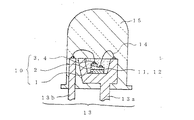
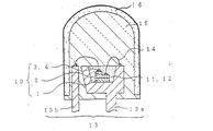
実施の形態1の発光装置は、サファイア基板1の上部に積層された半導体層2と、該半導体層2に形成された正負の電極3から延びる導電性ワイヤ14で導電接続されたリードフレーム13と、該サファイア基板1と該半導体層2とから構成される発光素子10の外周を覆うようにリードフレーム13aのカップ内に設けられた蛍光体11とコーティング部材12と、該蛍光体11及び該リードフレーム13の外周面を覆うモールド部材15と、から構成されている。
【0040】
サファイア基板1上に半導体層2が形成され、該半導体層2の同一平面側に正負の電極3が形成されている。前記半導体層2には、発光層(図示しない)が設けられており、この発光層から出力される発光ピーク波長は、紫外から青色領域の500nm以下近傍の発光スペクトルを有する。
【0041】
この発光素子10をダイボンダーにセットし、カップが設けられたリードフレーム13aにフェイスアップしてダイボンド(接着)する。ダイボンド後、リードフレーム13をワイヤーボンダーに移送し、発光素子の負電極3をカップの設けられたリードフレーム13aに金線でワイヤーボンドし、正電極3をもう一方のリードフレーム13bにワイヤーボンドする。
【0042】
次に、モールド装置に移送し、モールド装置のディスペンサーでリードフレーム13のカップ内に蛍光体11及びコーティング部材12を注入する。蛍光体11とコーティング部材12とは、あらかじめ所望の割合に均一に混合しておく。
【0043】
蛍光体11注入後、あらかじめモールド部材15が注入されたモールド型枠の中にリードフレーム13を浸漬した後、型枠をはずして樹脂を硬化させ、図1に示すような砲弾型の発光装置とする。
【0044】
(発光装置)
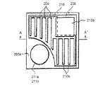
上記の実施の形態1の発光装置と異なる実施の形態2の発光装置についての具体的構成について詳述する。図2は、本発明に係る発光装置を示す図である。実施の形態2の発光装置は、表面実装型の発光装置を形成する。発光素子101は、紫外光励起の窒化物半導体発光素子を用いることができる。また、発光素子101は、青色光励起の窒化物半導体発光素子も用いることもできる。ここでは、紫外光励起の発光素子101を例にとって、説明する。発光素子101は、発光層として発光ピーク波長が約370nmのInGaN半導体を有する窒化物半導体発光素子を用いる。より具体的なLEDの素子構造としてサファイア基板上に、アンドープの窒化物半導体であるn型GaN層、Siドープのn型電極が形成されn型コンタクト層となるGaN層、アンドープの窒化物半導体であるn型GaN層、窒化物半導体であるn型AlGaN層、次に発光層を構成するInGaN層の単一量子井戸構造としてある。発光層上にはMgがドープされたp型クラッド層としてAlGaN層、Mgがドープされたp型コンタクト層であるGaN層を順次積層させた構成としてある。(なお、サファイア基板上には低温でGaN層を形成させバッファ層とさせてある。また、p型半導体は、成膜後400℃以上でアニールさせてある。)。エッチングによりサファイア基板上の窒化物半導体に同一面側で、pn各コンタクト層表面を露出させる。露出されたn型コンタクト層の上にn電極を帯状に形成し、切除されずに残ったp型コンタクト層のほぼ全面に、金属薄膜から成る透光性p電極が形成され、さらに透光性p電極の上にはn電極と平行に台座電極がスパッタリング法を用いて形成されている。
【0045】
次に、中央部に凹部を有し、且つ前記凹部の両側にコバール製のリード電極102が気密絶縁的に挿入固定されたベース部とからなるコバール製パッケージ105を用いる。前記パッケージ105及びリード電極102の表面にはNi/Ag層が設けられている。パッケージ105の凹部内に、Ag−Sn合金にて上述の発光素子101をダイボンドする。このように構成することにより、発光装置の構成部材を全て無機物とすることができ、発光素子101から放出される発光が紫外領域或いは可視光の短波長領域であったとしても飛躍的に信頼性の高い発光装置が得られる。
【0046】
次に、ダイボンドされた発光素子101の各電極と、パッケージ凹部底面から露出された各リード電極102とをそれぞれAgワイヤ104にて電気的導通を取る。パッケージの凹部内の水分を十分に排除した後、中央部にガラス窓部107を有するコバール製リッド106にて封止しシーム溶接を行う。ガラス窓部には、あらかじめニトロセルロース90wt%とγ−アルミナ10wt%からなるスラリーに対してCa2(Si1−XAlX)5N8:Ce(但し、0<X<1である、(Y1−xGdx)3(Al1−yGay)5O12:Ce(但し、0<x<1、0<y<1である。)等の蛍光体108を含有させ、リッド106の透光性窓部107の背面に塗布し、220℃にて30分間加熱硬化させることにより色変換部材を構成してある。こうして形成された発光装置を発光させると白色が高輝度に発光可能な発光ダイオードとすることができる。これによって色度調整が極めて簡単で量産性、信頼性に優れた発光装置とすることできる。以下、本発明の各構成について詳述する。
【0047】
以下、本発明に係る発光装置の構成部材について詳述する。
【0048】
(蛍光体11、108)
蛍光体11、108は、シリコンナイトライド系蛍光体が含まれている。また、蛍光体11、108は、シリコンナイトライド系蛍光体と第2の蛍光体とを組み合わせたものも使用することができる。本発明に係るシリコンナイトライド系蛍光体は、賦活剤にCeを必須とする少なくとも1種以上である希土類元素を用いており、Be、Mg、Ca、Sr、Ba、Znからなる群から選ばれる少なくとも1種以上である第II族元素と、C、Si、Ge、Sn、Ti、Zr、Hfからなる群から選ばれるSiを必須とする少なくとも1種以上である第IV族元素と、B、Al、Ga、In、Scからなる群から選ばれる少なくとも1種以上である第III族元素と、を少なくとも含有する。該元素の組合せは任意であるが、以下の組成のものを使用することが好ましい。該シリコンナイトライド系蛍光体は、LXMYTUOZN((2/3)X+(4/3)Y+U−(2/3)Z):R(Lは、Be、Mg、Ca、Sr、Ba、Znからなる群から選ばれる少なくとも1種以上である第II族元素である。Mは、C、Si、Ge、Sn、Ti、Zr、Hfからなる群から選ばれるSiを必須とする少なくとも1種以上である第IV族元素である。Tは、B、Al、Ga、In、Scからなる群から選ばれる少なくとも1種以上である第III族元素である。Oは、酸素元素である。Nは、窒素元素である。Rは、Ceを必須とする少なくとも1種以上である希土類元素である。X、Y、U、Zは、1.5<X<2.5、4.5<Y<5.5、0<U<0.5、0≦Z<1.0、または、0.5<X<1.5、6.5<Y<7.5、0<U<0.5、0≦Z<1.0、である。)の一般式で表される。前記X、Y、U、Zは、該範囲で高い輝度を示す。そのうち一般式中、前記X、前記Y、前記Zが、1.8<X<2.2、4.8<Y<5.2、若しくは、0.8<X<1.2、6.8<Y<7.2であることが好ましく、特に、前記X、前記Yが、X=2、Y=5、若しくは、X=1、Y=7であることが好ましい。該範囲のシリコンナイトライド系蛍光体は高い発光輝度を示すためである。但し、上記範囲に限定されず、任意のものも使用できる。また、シリコンナイトライド系蛍光体は、OとNとの比を変化させることで、色調や輝度を調節することができる。また、TとRのモル比を変化させることで、色調や輝度を調節することができる。このシリコンナイトライド系蛍光体の組成中には、Li、Na、K、Rb、Cs、Mn、Re、Cu、Ag、Auの少なくとも1種以上含有されていてもよい。これらを添加することにより輝度、量子効率等の発光効率を調整することができるからである。また、その他の元素も特性を損なわない程度に入っていても良い。但し、本発明は、この実施の形態及び実施例に限定されない。
【0049】
Lは、Be、Mg、Ca、Sr、Ba、Znからなる群から選ばれる少なくとも1種以上である第II族元素である。つまり、Ca、Sr、Ba等のいずれかを単体で用いてもよいが、BaとCa、BaとSr、CaとSr、BaとCaとSr等、種々組合せを変えることもできる。これらの第II族元素の混合物は、所望により配合比を変えることができる。
【0050】
Mは、C、Si、Ge、Sn、Ti、Hfからなる群から選ばれるSiを必須とする少なくとも1種以上である第IV族元素である。Mも、Siを単体で用いてもよいが、SiとGe、SiとC等、種々組合せを変えることもできる。Siを用いることにより安価で結晶性の良好な蛍光体を提供することができるからである。
【0051】
Rは、Ceを必須とする少なくとも1種以上である希土類元素である。具体的には、希土類元素は、Sc、Y、La、Ce、Pr、Nd、Sm、Eu、Gd、Tb、Dy、Ho、Er、Tm、Yb、Luである。これら希土類元素のうち、Ceを単体で用いてもよいが、Ceと希土類元素から選ばれる少なくとも1以上の元素と、を含んでいるものも使用することもできる。Ce以外の元素は、共賦活剤として、作用するためである。Rは、Ceが70重量%以上含有されていることが好ましい。特に、Rは、第II族元素に対して、モル比で、第II族元素:R=1:0.005乃至1:0.5である。
【0052】
発光中心に希土類元素であるセリウムCeを用いる。本発明では、Ceのみを用いて説明するが、これに限定されず、Ceと共賦活させたものも使用することができる。セリウムは、+4価を生じやすく、他の希土類元素を分離しやすい。Ceは、Cl2、Br2と反応して、CeCl3、CeBr3を与える。空気中で徐々に、高温で速やかに酸化されCeO2となる。水とは徐々に、酸水溶液とは速やかにH2を発生して溶けCe3+となる。安定な酸化数は他の希土類元素と同様+IIIであるが、+IVもとりやすい。セリウム化合物は、+IIIの酸化状態が最も安定であるが、+IVも溶液中でかなり安定に存在する。本発明の蛍光体は、母体のアルカリ土類金属系窒化ケイ素に対して、Ce3+を賦活剤として用いる。
【0053】
母体材料として、主成分のL、Mも、それぞれの化合物を使用することができる。これらは、金属、酸化物、イミド、アミド、窒化物及び各種塩類などを用いることができる。また、あらかじめ主成分のL、Mの元素を混合し、使用してもよい。
【0054】
Tは、B、Al、Ga、In、Scからなる群から選ばれる少なくとも1種以上である第III族元素である。Tも、金属、酸化物、イミド、アミド、窒化物及び各種塩類などを原料として用いることができる。例えば、B2O6、H3BO3、Al2O3、Al(NO3)3・9H2O、AlN、GaCl3、InCl3等である。
【0055】
Lの窒化物、Mの窒化物、Tの酸化物を母体材料として、混合する。該母体材料中に、Ceの酸化物を賦活剤として混入する。これらを所望量計り、均一になるまで混合する。これらの母体材料を、LXMYTUOZN((2/3)X+( 4/3)Y+U−(2/3)Z):Rの組成比となるように、所定量を秤量して混合する。
【0056】
(シリコンナイトライド系蛍光体の製造方法)
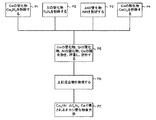
次に、本発明に係るシリコンナイトライド系蛍光体、Ca2(Si,Al)5N8:Ceの製造方法を説明するが、本製造方法に限定されない。図3は、シリコンナイトライド系蛍光体の製造方法を示す工程図である。
【0057】
あらかじめCaの窒化物、Siの窒化物、Alの窒化物、Ceの酸化物を準備する。これら原料は、精製したものを用いる方が良いが、市販のものを用いても良い。具体的には、以下の方法によりシリコンナイトライド系蛍光体を製造する。
【0058】
原料にCaの窒化物Ca3N2を使用する。原料は、Caの単体を使用することが好ましいが、イミド化合物、アミド化合物、CaOなどの化合物を使用することもできる。また原料Caは、B、Ga、K、Naなどを含有するものでもよい。
【0059】
Caの窒化物Ca3N2を粉砕する(P1)。Caの窒化物を、アルゴン雰囲気中、若しくは、窒素雰囲気中、グローブボックス内で粉砕を行う。
【0060】
原料にSiの窒化物Si3N4を使用する。原料は、Siの単体を使用することが好ましいが、窒化物化合物、イミド化合物、アミド化合物などを使用することもできる。例えば、Si3N4、Si(NH2)2、Mg2Si、Ca2Si、SiCなどである。原料のSiの純度は、3N以上のものが好ましいが、B、Ga、K、Naなどが含有されていてもよい。
【0061】
Siの窒化物Si3N4を粉砕する(P2)。Siの窒化物を、アルゴン雰囲気中、若しくは、窒素雰囲気中、グローブボックス内で粉砕を行う。
【0062】
Alの窒化物AlNを粉砕する(P3)。Alの窒化物に代えて、第III族元素であるB、Ga、In、Sc、例えば、H3BO3、Ga2O3、In2O3、Sc2O3などを用いることができるが、これに限定されない。
【0063】
原料にCeの酸化物CeO2を使用する。原料は、Ceの単体を使用することが好ましいが、セリウム化合物を使用することもできる。
【0064】
Ceの酸化物CeO2を粉砕する(P4)。
【0065】
上記の原料Caの窒化物Ca3N2、Siの窒化物Si3N4、Alの窒化物AlN、Ceの酸化物CeO2を秤量して、混合する(P5)。上記原料を、所定の配合比になるように、所定のモル量を秤量する。
【0066】
次に、Caの窒化物、Siの窒化物、Alの窒化物、Ceの酸化物の混合物を焼成する(P6)。当該混合物を坩堝に投入し、焼成を行う。
【0067】
混合及び焼成により、Ca2(Si,Al)5N8:Ceで表されるシリコンナイトライド系蛍光体を得ることができる(P7)。
【0068】
ただし、この組成は、配合比率より推定される代表組成であり、その比率の近傍では、実用に耐える十分な特性を有する。また、各原料の配合比率を変更することにより、目的とする蛍光体の組成を変更することができる。
【0069】
焼成は、管状炉、箱型炉、高周波炉、メタル炉などを使用することができる。焼成温度は、特に限定されないが、1200から2000℃の範囲で焼成を行うことが好ましく、1400から1700℃の焼成温度が、さらに好ましい。
【0070】
また、焼成は、還元雰囲気中で行うことが好ましい。還元雰囲気は、窒素雰囲気、窒素−水素雰囲気、アンモニア雰囲気、アルゴン等の不活性ガス雰囲気等である。
【0071】
以上の製造方法を使用することにより、目的とするシリコンナイトライド系蛍光体を得ることが可能である。
【0072】
(第2の蛍光体11、108)
蛍光体11、108中には、シリコンナイトライド系蛍光体と共に、第2の蛍光体が含まれている。第2の蛍光体としては、Eu等のランタノイド系、Mn等の遷移金属系の元素により主に賦活されるアルカリ土類ハロゲンアパタイト蛍光体、アルカリ土類金属ホウ酸ハロゲン蛍光体、アルカリ土類金属アルミン酸塩蛍光体、アルカリ土類ケイ酸塩、アルカリ土類硫化物、アルカリ土類チオガレート、アルカリ土類窒化ケイ素、ゲルマン酸塩、又は、Ce等のランタノイド系元素で主に賦活される希土類アルミン酸塩、希土類ケイ酸塩、又は、Eu等のランタノイド系元素で主に賦活される有機及び有機錯体等から選ばれる少なくともいずれか1以上であることが好ましい。具体例として、下記の蛍光体を使用することができるが、これに限定されない。
【0073】
Eu等のランタノイド系、Mn等の遷移金属系の元素により主に賦活されるアルカリ土類ハロゲンアパタイト蛍光体には、M5(PO4)3X:R(Mは、Sr、Ca、Ba、Mg、Znから選ばれる少なくとも1種以上である。Xは、F、Cl、Br、Iから選ばれる少なくとも1種以上である。Rは、Eu、Mn、EuとMn、のいずれか1以上である。)などがある。
【0074】
アルカリ土類金属ホウ酸ハロゲン蛍光体には、M2B5O9X:R(Mは、Sr、Ca、Ba、Mg、Znから選ばれる少なくとも1種以上である。Xは、F、Cl、Br、Iから選ばれる少なくとも1種以上である。Rは、Eu、Mn、EuとMn、のいずれか1以上である。)などがある。
【0075】
アルカリ土類金属アルミン酸塩蛍光体には、SrAl2O4:R、Sr4Al14O25:R、CaAl2O4:R、BaMg2Al16O27:R、BaMg2Al16O12:R、BaMgAl10O17:R(Rは、Eu、Mn、EuとMn、のいずれか1以上である。)などがある。
【0076】
希土類酸硫化物蛍光体には、La2O2S:Eu、Y2O2S:Eu、Gd2O2S:Euなどがある。
【0077】
アルカリ土類金属硫化物蛍光体には、CaS:Ce3+、CaS:Eu2+、CaS:Mn2+などがある。
【0078】
Ce等のランタノイド系元素で主に賦活される希土類アルミン酸塩蛍光体には、Y3Al5O12:Ce、(Y0.8Gd0.2)3Al5O12:Ce、Y3(Al0.8Ga0.2)5O12:Ce、(Y,Gd)3(Al,Ga)5O12の組成式で表されるYAG系蛍光体などがある。
【0079】
その他の蛍光体には、ZnS:Mn、Zn2GeO4:Mn、MGa2S4:Eu(Mは、Sr、Ca、Ba、Mg、Znから選ばれる少なくとも1種以上である。Xは、F、Cl、Br、Iから選ばれる少なくとも1種以上である。)などがある。また、M2Si5N8:Eu、MSi7N10:Eu、M1.8Si5O0.2N8:Eu、M0.9Si7O0.1N10:Eu(Mは、Sr、Ca、Ba、Mg、Znから選ばれる少なくとも1種以上である。)などもある。
【0080】
上述の第2の蛍光体は、所望に応じてEuに代えて、又は、Euに加えてTb、Cu、Ag、Au、Cr、Nd、Dy、Co、Ni、Tiから選択される1種以上を含有させることもできる。
【0081】
また、上記蛍光体以外の蛍光体であって、同様の性能、効果を有する蛍光体も使用することができる。
【0082】
これらの第2の蛍光体は、発光素子10、101の励起光により、黄色、赤色、緑色、青色に発光スペクトルを有する蛍光体を使用することができるほか、これらの中間色である黄色、青緑色、橙色などに発光スペクトルを有する蛍光体も使用することができる。これらの第2の蛍光体は、1種類に限らず、異なる種類の蛍光体と組み合わせて使用することにより、種々の発光色を有する発光装置を製造することができる。
【0083】
例えば、第2の蛍光体として緑色から黄色に発光するCaSi2O2N2:Eu、又はSrSi2O2N2:Euと、青色に発光する(Sr,Ca)5(PO4)3Cl:Eu、赤色に発光する(Ca,Sr)2Si5N8:Euと、からなる蛍光体11、108を使用することによって、演色性の良好な白色に発光する発光装置を提供することができる。これは、光の三源色である赤・青・緑を使用しているため、第1の蛍光体及び第2の蛍光体の配合比を変えることのみで、所望の白色光を実現することができる。特に、励起光源に460nm近傍の光を用いて、シリコンナイトライド系蛍光体と第2の蛍光体に照射させたとき、シリコンナイトライド系蛍光体が500〜610nm辺りの緑色から黄赤色の光を発光する。これにより、演色性に優れた白色系発光装置を提供することができる。
【0084】
上記蛍光体11、108の粒径は、1μm〜20μmの範囲が好ましく、より好ましくは2μm〜8μmである。特に、5μm〜8μmが好ましい。2μmより小さい粒径を有する蛍光体は、凝集体を形成しやすい傾向にある。一方、5μm〜8μmの粒径範囲の蛍光体は、光の吸収率及び変換効率が高い。このように、光学的に優れた特徴を有する粒径の大きな蛍光体を含有させることにより、発光装置の量産性が向上する。
【0085】
ここで粒径は、空気透過法で得られる平均粒径を指す。具体的には、気温25℃、湿度70%の環境下において、1cm3分の試料を計り取り、専用の管状容器にパッキングした後、一定圧力の乾燥空気を流し、差圧から比表面積を読みとり、平均粒径に換算した値である。本発明で用いられる蛍光体の平均粒径は2μm〜8μmの範囲であることが好ましい。また、この平均粒径値を有する蛍光体が、頻度高く含有されていることが好ましい。また、粒度分布も狭い範囲に分布しているものが好ましく、特に、微粒子2μm以下の少ないものが好ましい。このように粒径、及び粒度分布のバラツキが小さい蛍光体を用いることにより、より色ムラが抑制され、良好な色調を有する発光装置が得られる。
【0086】
発光装置2における蛍光体108の配置場所は発光素子101との位置関係において種々の場所に配置することができる。例えば、発光素子101を被覆するモールド材料中に、蛍光体108を含有させることができる。また、発光素子101と蛍光体108とを、間隙をおいて配置しても良いし、発光素子101の上部に蛍光体108を、直接載置しても良い。
【0087】
(コーティング部材12、109)
蛍光体11、108は、有機材料である樹脂や無機材料であるガラスなど種々のコーティング部材(バインダー)を用いて、付着させることができる。コーティング部材12、109は、蛍光体11、108を発光素子10、101や窓部107等に固着させるためのバインダーとしての役割を有することもある。コーティング部材(バインダー)として有機物を使用する場合、具体的材料として、エポキシ樹脂、アクリル樹脂、シリコーンなどの耐候性に優れた透明樹脂が好適に用いられる。特に、シリコーンを用いると、信頼性に優れ、且つ蛍光体11、108の分散性を向上させることができ好ましい。
【0088】
また、コーティング部材(バインダー)12、109として、窓部107の熱膨張率と近似である無機物を使用すると、蛍光体108を良好に前記窓部107に密着させることができ好ましい。具体的方法として、沈降法やゾル−ゲル法、スプレー法等を用いることができる。例えば、蛍光体11、108に、シラノール(Si(OEt)3OH)、及びエタノールを混合してスラリーを形成し、該スラリーをノズルから吐出させた後、300℃にて3時間加熱してシラノールをSiO2とし、蛍光体を所望の場所に固着させることができる。
【0089】
また、無機物である結着剤をコーティング部材(バインダー)12、109として用いることもできる。結着剤とは、いわゆる低融点ガラスであり、微細な粒子であり、且つ紫外から可視領域の輻射線に対して吸収が少なく、コーティング部材(バインダー)12、109中にて極めて安定であることが好ましい。
【0090】
また、粒径の大きな蛍光体をコーティング部材(バインダー)12、109に付着させる場合、融点が高くても粒子が超微粉体である結着剤、例えば、シリカ、アルミナ、あるいは沈殿法で得られる細かい粒度のアルカリ土類金属のピロリン酸塩、正りん酸塩などを使用することが好ましい。これらの結着剤は、単独、若しくは互いに混合して用いることができる。
【0091】
ここで、上記結着剤の塗布方法について述べる。結着剤は、結着効果を十分に高めるため、ビヒクル中に湿式粉砕して、スラリー状にして、結着剤スラリーとして用いることが好ましい。前記ビヒクルとは、有機溶媒あるいは脱イオン水に少量の粘結剤を溶解して得られる高粘度溶液である。例えば、有機溶媒である酢酸ブチルに対して粘結剤であるニトロセルロースを1wt%含有させることにより、有機系ビヒクルが得られる。
【0092】
このようにして得られた結着剤スラリーに、蛍光体11、108を含有させて塗布液を作製する。塗布液中のスラリーの添加量は、塗布液中の蛍光体量に対してスラリー中の結着剤の総量が、1〜3%wt程度とすることができる。光束維持率の低下を抑制するため、結着剤の添加量が少ない方が好ましい。
【0093】
前記塗布液を前記窓部107の背面に塗布する。その後、温風あるいは熱風を吹き込み乾燥させる。最後に400℃〜700℃の温度でベーキングを行い、前記ビヒクルを飛散させる。これにより所望の場所に蛍光体層が結着剤にて付着される。
【0094】
(発光素子10、101)
本発明において発光素子10、101は、蛍光体を効率よく励起可能な発光ピーク波長を発光できる発光層を有する半導体発光素子が好ましい。このような半導体発光素子の材料として、BN、SiC、ZnSeやGaN、InGaN、InAlGaN、AlGaN、BAlGaN、BInAlGaNなど種々の半導体を挙げることができる。同様に、これらの元素に不純物元素としてSiやZnなどを含有させ発光中心とすることもできる。蛍光体11、108を効率良く励起できる紫外領域から可視光の短波長を効率よく発光可能な発光層の材料として特に、窒化物半導体(例えば、AlやGaを含む窒化物半導体、InやGaを含む窒化物半導体としてInXAlYGa1−X−YN、0≦X、0≦Y、X+Y≦1)がより好適に挙げられる。
【0095】
また、半導体の構造としては、MIS接合、PIN接合やpn接合などを有するホモ構造、ヘテロ構造あるいはダブルへテロ構成のものが好適に挙げられる。半導体層の材料やその混晶比によって発光ピーク波長を種々選択することができる。また、半導体活性層を量子効果が生ずる薄膜に形成させた単一量子井戸構造や多重量子井戸構造とすることでより出力を向上させることもできる。
【0096】
発光素子10、101に、窒化物半導体を使用した場合、半導体用基板にはサファイア、スピネル、SiC、Si、ZnO、GaAs、GaN等の材料が好適に用いられる。結晶性の良い窒化物半導体を量産性よく形成させるためにはサファイア基板を利用することが好ましい。このサファイア基板上にHVPE法やMOCVD法などを用いて窒化物半導体を形成させることができる。サファイア基板上にGaN、AlN、GaAIN等の低温で成長させ非単結晶となるバッファ層を形成しその上にpn接合を有する窒化物半導体を形成させる。
【0097】
窒化物半導体を使用したpn接合を有する紫外領域を効率よく発光可能な発光素子例として、バッファ層上に、サファイア基板のオリフラ面と略垂直にSiO2をストライプ状に形成する。ストライプ上にHVPE法を用いてGaNをELOG(Epitaxial Lateral Over Grows GaN)成長させる。続いて、MOCVD法により、n型窒化ガリウムで形成した第1のコンタクト層、n型窒化アルミニウム・ガリウムで形成させた第1のクラッド層、窒化インジウム・アルミニウム・ガリウムの井戸層と窒化アルミニウム・ガリウムの障壁層を複数積層させた多重量子井戸構造とされる活性層、p型窒化アルミニウム・ガリウムで形成した第2のクラッド層、p型窒化ガリウムで形成した第2のコンタクト層を順に積層させたダブルへテロ構成などの構成が挙げられる。活性層をリッジストライプ形状としガイド層で挟むと共に共振器端面を設け本発明に利用可能な半導体レーザー素子とすることもできる。
【0098】
窒化物半導体は、不純物をドープしない状態でn型導電性を示す。発光効率を向上させるなど所望のn型窒化物半導体を形成させる場合は、n型ドーパントとしてSi、Ge、Se、Te、C等を適宜導入することが好ましい。一方、p型窒化物半導体を形成させる場合は、p型ドーパントであるZn、Mg、Be、Ca、Sr、Ba等をドープさせることが好ましい。窒化物半導体は、p型ドーパントをドープしただけではp型化しにくいためp型ドーパント導入後に、炉による加熱やプラズマ照射等により低抵抗化させることが好ましい。サファイア基板をとらない場合は、第1のコンタクト層の表面までp型側からエンチングさせコンタクト層を露出させる。各コンタクト層上にそれぞれ電極形成後、半導体ウェハーからチップ状にカットさせることで窒化物半導体からなる発光素子を形成させることができる。
【0099】
本発明の発光装置において、量産性よく形成させるためには、蛍光体11、108を発光素子10、101に固着する際に、樹脂を利用して形成することが好ましい。この場合、蛍光体11、108からの発光ピーク波長と透光性樹脂の劣化等を考慮して、発光素子10、101は紫外域に発光スペクトルを有し、その発光ピーク波長は、360nm以上420nm以下のものや、450nm以上470nm以下のものを使用することが好ましい。
【0100】
ここで、本発明で用いられる半導体発光素子10、101は、不純物濃度1017〜1020/cm3で形成されるn型コンタクト層のシート抵抗と、透光性p電極のシート抵抗とが、Rp≧Rnの関係となるように調節されていることが好ましい。n型コンタクト層は、例えば膜厚3〜10μm、より好ましくは4〜6μmに形成されると好ましく、そのシート抵抗は10〜15Ω/□と見積もられることから、このときのRpは前記シート抵抗値以上のシート抵抗値を有するように薄膜に形成するとよい。また、透光性p電極は、膜厚が150μm以下の薄膜で形成されていてもよい。
【0101】
また、透光性p電極が、金および白金族元素の群から選択された1種と、少なくとも1種の他の元素とから成る多層膜または合金で形成される場合には、含有されている金または白金族元素の含有量により透光性p電極のシート抵抗の調整をすると安定性および再現性が向上される。金または金属元素は、本発明に使用する半導体発光素子の波長領域における吸収係数が高いので、透光性p電極に含まれる金又は白金族元素の量は少ないほど透過性がよくなる。従来の半導体発光素子はシート抵抗の関係がRp≦Rnであったが、本発明ではRp≧Rnであるので、透光性p電極は従来のものと比較して薄膜に形成されることとなるが、このとき金または白金族元素の含有量を減らすことで薄膜化が容易に行える。
【0102】
上述のように、本発明で用いられる半導体発光素子10、101は、n型コンタクト層のシート抵抗RnΩ/□と、透光性p電極のシート抵抗RpΩ/□とが、Rp≧Rnの関係を成していることが好ましい。半導体発光素子10、101として形成した後にRnを測定するのは難しく、RpとRnとの関係を知るのは実質上不可能であるが、発光時の光強度分布の状態からどのようなRpとRnとの関係になっているのかを知ることができる。
【0103】
透光性p電極とn型コンタクト層とがRp≧Rnの関係であるとき、前記透光性p電極上に接して延長伝導部を有するp側台座電極を設けると、さらなる外部量子効率の向上を図ることができる。延長伝導部の形状及び方向に制限はなく、延長伝導部が衛線上である場合、光を遮る面積が減るので好ましいが、メッシュ状でもよい。また形状は、直線状以外に、曲線状、格子状、枝状、鉤状でもよい。このときp側台座電極の総面積に比例して遮光効果が増大するため、遮光効果が発光増強効果を上回らないように延長導電部の線幅及び長さを設計するのがよい。
【0104】
(発光素子10、101)
発光素子10、101は、上述の紫外発光の発光素子と異なる青色系に発光する発光素子を使用することもできる。青色系に発光する発光素子10、101は、III族窒化物系化合物発光素子であることが好ましい。発光素子10、101は、例えばサファイア基板1上にGaNバッファ層を介して、Siがアンドープのn型GaN層、Siがドープされたn型GaNからなるn型コンタクト層、アンドープGaN層、多重量子井戸構造の発光層(GaN障壁層/InGaN井戸層の量子井戸構造)、Mgがドープされたp型GaNからなるp型GaNからなるpクラッド層、Mgがドープされたp型GaNからなるp型コンタクト層が順次積層された積層構造を有し、以下のように電極が形成されている。但し、この構成と異なる発光素子も使用できる。
【0105】
pオーミック電極は、p型コンタクト層上のほぼ全面に形成され、そのpオーミック電極上の一部にpパッド電極が形成される。
【0106】
また、n電極は、エッチングによりp型コンタクト層からアンドープGaN層を除去してn型コンタクト層の一部を露出させ、その露出された部分に形成される。
【0107】
なお、本実施の形態では、多重量子井戸構造の発光層を用いたが、本発明は、これに限定されるものではなく、例えば、InGaNを利用した単一量子井戸構造としても良いし、Si、ZnがドープされたGaNを利用しても良い。
【0108】
また、発光素子10、101の発光層は、Inの含有量を変化させることにより、420nmから490nmの範囲において主発光ピーク波長を変更することができる。また、発光ピーク波長は、上記範囲に限定されるものではなく、360〜550nmに発光ピーク波長を有しているものを使用することができる。
【0109】
(コーティング部材12、109)
コーティング部材12(光透光性材料)は、リードフレーム13のカップ内に設けられるものであり発光素子10の発光を変換する蛍光体11と混合して用いられる。コーティング部材12の具体的材料としては、エポキシ樹脂、ユリア樹脂、シリコーン樹脂などの温度特性、耐候性に優れた透明樹脂、シリカゾル、ガラス、無機バインダーなどが用いられる。また、蛍光体と共に拡散剤、チタン酸バリウム、酸化チタン、酸化アルミニウムなどを含有させても良い。また、光安定化剤や着色剤を含有させても良い。
【0110】
(リードフレーム13)
リードフレーム13は、マウントリード13aとインナーリード13bとから構成される。
【0111】
マウントリード13aは、発光素子10を配置させるものである。マウントリード13aの上部は、カップ形状になっており、カップ内に発光素子10をダイボンドし、該発光素子10の外周面を、カップ内を前記蛍光体11と前記コーティング部材12とで覆っている。カップ内に発光素子10を複数配置しマウントリード13aを発光素子10の共通電極として利用することもできる。この場合、十分な電気伝導性と導電性ワイヤ14との接続性が求められる。発光素子10とマウントリード13aのカップとのダイボンド(接着)は、熱硬化性樹脂などによって行うことができる。熱硬化性樹脂としては、エポキシ樹脂、アクリル樹脂、イミド樹脂などが挙げられる。また、フェースダウン発光素子10などによりマウントリード13aとダイボンドすると共に電気的接続を行うには、Ag―エースと、カーボンペースト、金属バンプなどを用いることができる。また、無機バインダーを用いることもできる。
【0112】
インナーリード13bは、マウントリード13a上に配置された発光素子10の電極3から延びる導電性ワイヤ14との電気的接続を図るものである。インナーリード13bは、マウントリード13aとの電気的接触によるショートを避けるため、マウントリード13aから離れた位置に配置することが好ましい。マウントリード13a上に複数の発光素子10を設けた場合は、各導電性ワイヤ同士が接触しないように配置できる構成にする必要がある。インナーリード13bは、マウントリード13aと同様の材質を用いることが好ましく、鉄、銅、鉄入り銅、金、白金、銀などを用いることができる。
【0113】
(導電性ワイヤ)
導電性ワイヤ14は、発光素子10の電極3とリードフレーム13とを電気的に接続するものである。導電性ワイヤ14は、電極3とオーミック性、機械的接続性、電気導電性及び熱伝導性が良いものが好ましい。導電性ワイヤ14の具体的材料としては、金、銅、白金、アルミニウムなどの金属及びそれらの合金などが好ましい。
【0114】
(モールド部材)
モールド部材15は、発光素子10、蛍光体11、コーティング部材12、リードフレーム13及び導電性ワイヤ14などを外部から保護するために設けられている。モールド部材15は、外部からの保護目的の他に、視野角を広げたり、発光素子10からの指向性を緩和したり、発光を収束、拡散させたりする目的も併せ持っている。これらの目的を達成するためモールド部材は、所望の形状にすることができる。また、モールド部材15は、凸レンズ形状、凹レンズ形状の他、複数積層する構造であっても良い。モールド部材15の具体的材料としては、エポキシ樹脂、ユリア樹脂、シリコーン樹脂、シリカゾル、ガラスなどの透光性、耐候性、温度特性に優れた材料を使用することができる。モールド部材15には、拡散剤、着色剤、紫外線吸収剤や蛍光体を含有させることもできる。拡散剤としては、チタン酸バリウム、酸化チタン、酸化アルミニウム等が好ましい。コーティング部材12との材質の反発性を少なくするため、屈折率を考慮するため、同材質を用いることが好ましい。
【0115】
以下、本発明に係る蛍光体、発光装置について実施例を挙げて説明するが、この実施例に限定されるものではない。
【0116】
なお、温度特性は、25℃の発光輝度を100%とする相対輝度で示す。粒径は、前述の平均粒径を示し、F.S.S.S.No.(Fisher Sub Sieve Sizer's No.)という空気透過法による値である。
【0117】
【実施例】
以下、本発明の実施例について詳述する。
【0118】
(蛍光体)
<実施例1乃至4>
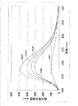
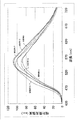
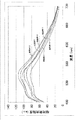
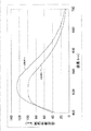
図4は、実施例1乃至4及び比較例1のシリコンナイトライド系蛍光体を波長400nmの光で励起したときの発光スペクトルを示す図である。図5は、実施例1乃至4及び比較例1のシリコンナイトライド系蛍光体を波長460nmの光で励起したときの発光スペクトルを示す図である。図6(a)乃至(c)は、実施例3のシリコンナイトライド系蛍光体を撮影したSEM写真(走査電子顕微鏡)である。図6(d)乃至(f)は、比較例1のシリコンナイトライド系蛍光体を撮影したSEM写真である。図6(a)及び(d)は1000倍、(b)及び(e)は5000倍、(c)及び(f)は10000倍で撮影したものである。図14は、実施例1乃至4及び比較例1のシリコンナイトライド系蛍光体の励起スペクトルを示す図である。
【0119】
実施例1乃至4は、Caの一部をCeで置換している。実施例1乃至4は、共賦活剤として作用するAlの濃度を変えている。実施例1は、(Ca0.955Ce0.045)2(Si0.991Al0.009)5N8である。実施例2は、(Ca0.955Ce0.045)2(Si0.982Al0.018)5N8である。実施例3は、(Ca0.955Ce0.045)2(Si0.964Al0.036)5N8である。実施例4は、(Ca0.955Ce0.045)2(Si0.928Al0.072)5N8である。
【0120】
まず、原料は、Ca3N2、Si3N4、AlN、CeO2を使用した。該原料を、それぞれ0.1〜3.0μmに粉砕した。粉砕後、実施例1は、上記組成となるように、下記の重量の原料を使用した。ここで、Caに対してCeのモル比は、Ca:Ce=0.955:0.045である。
Ca3N2:2.748g
Si3N4:6.745g
AlN:0.054g
CeO2:0.451g
実施例2乃至4も、実施例1と同様に、上記組成となるように、原料の秤量を行った。
【0121】
上記重量を秤量した後、Ca3N2、Si3N4、AlN、CeO2を、均一になるまで混合した。
【0122】
上記化合物を混合し、坩堝に投入し、アンモニア雰囲気中で、約1550℃で約5時間、焼成を行った。
【0123】
これにより、目的とするシリコンナイトライド系蛍光体を得た。
【0124】
実施例1乃至4の焼成品は、いずれも、結晶性の粉体若しくは粒体である。粒径は、ほぼ1〜5μmであった。
【0125】
なお、実施例1乃至15の酸素濃度は、Si5モルに対して、1モル以下であった。但し、酸素濃度は、焼成条件によって異なる。
【0126】
比較例1は、AlNを添加していない点を除いて、実施例1と、同条件で焼成を行った。(Ca0.955Ce0.045)2Si5N8である。下記の重量の原料を秤量した。
Ca3N2:2.746g
Si3N4:6.803g
CeO2:0.451g
表1は、実施例1乃至4及び比較例1のシリコンナイトライド系蛍光体を波長400nm、460nmの光で励起させたときの発光特性を示す。
【0127】
【表1】
【0128】
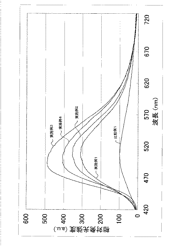
励起光源として、波長400nm近傍の光を実施例1乃至4及び比較例1のシリコンナイトライド系蛍光体に照射して励起させた。その結果、実施例1のシリコンナイトライド系蛍光体は、色調x=0.261、色調y=0.426、発光ピーク波長λp=506nmの緑色領域に発光色を有する。実施例3は、色調x=0.253、色調y=0.429、λp=493nmの青緑から緑色領域に発光色を有する。実施例1乃至3のシリコンナイトライド系蛍光体のいずれも、比較例1のシリコンナイトライド系蛍光体よりも、高い発光効率を示した。特に、実施例3のシリコンナイトライド系蛍光体は、比較例1のシリコンナイトライド系蛍光体よりも365.0%もの極めて高い発光輝度、344.6%もの極めて高いエネルギー効率、330.6%もの極めて高い量子効率を示した。なお、実施例1乃至4は、比較例1の発光輝度、エネルギー効率、量子効率を100%として、その相対値で表す。
【0129】
励起光源として、波長460nm近傍の光を実施例1乃至4及び比較例1のシリコンナイトライド系蛍光体に照射して励起させた。その結果、実施例4のシリコンナイトライド系蛍光体は、比較例1のシリコンナイトライド系蛍光体よりも210.0%もの高い発光輝度、171.4%もの高いエネルギー効率、156.9%もの高い量子効率を示した。
【0130】
また、シリコンナイトライド系蛍光体は、極めて良好な温度特性を示す。
【0131】
これら上記シリコンナイトライド系蛍光体のX線回折像を測定したところ、いずれもシャープな回折ピークを示し、得られた蛍光体が、規則性を有する結晶性の化合物であった。比較例1に比べて、実施例3の粒径は大きく、小粒径のものが少ない。また、実施例3の粒形の方が、均一である。
【0132】
<実施例5乃至9>
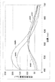
図7は、実施例5乃至9及び比較例2のシリコンナイトライド系蛍光体を波長400nmの光で励起したときの発光スペクトルを示す図である。図8は、実施例5乃至9及び比較例2のシリコンナイトライド系蛍光体を波長460nmの光で励起したときの発光スペクトルを示す図である。図14は、実施例5乃至9及び比較例2のシリコンナイトライド系蛍光体の励起スペクトルを示す図である。
【0133】
実施例5乃至9は、Caの一部をCeで置換している。実施例5乃至9は、共賦活剤の種類を変えている。共賦活剤のモル濃度は、Siに対して、Si:共賦活剤=0.982:0.018である。実施例5は、(Ca0.955Ce0.045)2(Si0.982B0.018)5N8である。実施例6は、(Ca0.955Ce0.045)2(Si0.982Al0.018)5N8である。実施例7は、(Ca0.955Ce0.045)2(Si0.982Ga0.018)5N8である。実施例8は、(Ca0.955Ce0.045)2(Si0.982In0.018)5N8、実施例9は、(Ca0.955Ce0.045)2(Si0.982Sc0.018)5N8である。
【0134】
原料は、Ca3N2、Si3N4、CeO2、及び共賦活剤H3BO3、AlN、Ga2O3、In2O3、Sc2O3を使用した。実施例5乃至9は、実施例1とほぼ同様の方法により製造を行った。まず、上記原料を、それぞれ0.1〜3.0μmに粉砕した。粉砕後、実施例5乃至9は、上記組成となるように、原料の秤量を行った。ここで、Caに対してCeのモル比は、Ca:Ce=0.955:0.045である。
【0135】
上記重量を秤量した後、Ca3N2、Si3N4、CeO2及び共賦活剤を、均一になるまで混合した。
【0136】
上記化合物を混合し、坩堝に投入し、アンモニア雰囲気中で、約1350℃で約4時間、焼成を行った。
【0137】
これにより、目的とするシリコンナイトライド系蛍光体を得た。
【0138】
実施例5乃至9の焼成品は、いずれも、結晶性の粉体若しくは粒体である。粒径は、ほぼ1〜5μmであった。
【0139】
比較例2は、共賦活剤を添加していない点を除いて、実施例5乃至9と、同条件で焼成を行った。(Ca0.955Ce0.045)2Si5N8である。
【0140】
表2は、実施例5乃至9及び比較例2のシリコンナイトライド系蛍光体を波長400nm、460nmの光で励起させたときの発光特性を示す。
【0141】
【表2】
【0142】
励起光源として、波長460nm近傍の光を実施例5乃至9及び比較例2のシリコンナイトライド系蛍光体に照射して励起させた。その結果、実施例8のシリコンナイトライド系蛍光体は、比較例2のシリコンナイトライド系蛍光体よりも168.2%もの高い発光輝度、139.3%もの高いエネルギー効率、129.3%もの高い量子効率を示した。
【0143】
また、シリコンナイトライド系蛍光体は、極めて良好な温度特性を示す。
【0144】
これら上記シリコンナイトライド系蛍光体のX線回折像を測定したところ、いずれもシャープな回折ピークを示し、得られた蛍光体が、規則性を有する結晶性の化合物であった。
【0145】
<実施例10乃至14>
図9は、実施例10乃至14及び比較例3のシリコンナイトライド系蛍光体を波長400nmの光で励起したときの発光スペクトルを示す図である。図10は、実施例10乃至14及び比較例3のシリコンナイトライド系蛍光体を波長460nmの光で励起したときの発光スペクトルを示す図である。図14は、実施例10乃至14及び比較例3のシリコンナイトライド系蛍光体の励起スペクトルを示す図である。
【0146】
実施例10乃至14は、Srの一部をCeで置換している。実施例10乃至14は、共賦活剤の種類を変えている。共賦活剤のモル濃度は、Siに対して、Si:共賦活剤=0.982:0.018である。実施例10は、(Sr0.955Ce0.045)2(Si0.982B0.018)5N8である。実施例11は、(Sr0.955Ce0.045)2(Si0.982Al0.018)5N8である。実施例12は、(Sr0.955Ce0.045)2(Si0.982Ga0.018)5N8である。実施例13は、(Sr0.955Ce0.045)2(Si0.982In0.018)5N8、実施例14は、(Sr0.955Ce0.045)2(Si0.982Sc0.018)5N8である。
【0147】
原料は、Sr3N2、Si3N4、CeO2、及び共賦活剤H3BO3、AlN、Ga2O3、In2O3、Sc2O3を使用した。実施例10乃至14は、実施例1とほぼ同様の方法により製造を行った。まず、上記原料を、それぞれ0.1〜3.0μmに粉砕した。粉砕後、実施例10乃至14は、上記組成となるように、原料の秤量を行った。ここで、Srに対してCeのモル比は、Sr:Ce=0.955:0.045である。
【0148】
上記重量を秤量した後、Sr3N2、Si3N4、CeO2及び共賦活剤を、均一になるまで混合した。
【0149】
上記化合物を混合し、坩堝に投入し、アンモニア雰囲気中で、約1350℃で約4時間、焼成を行った。
【0150】
これにより、目的とするシリコンナイトライド系蛍光体を得た。
【0151】
実施例10乃至14の焼成品は、いずれも、結晶性の粉体若しくは粒体である。粒径は、ほぼ1〜5μmであった。
【0152】
比較例3は、共賦活剤を添加していない点を除いて、実施例10乃至14と、同条件で焼成を行った。(Sr0.955Ce0.045)2Si5N8である。
【0153】
表3は、実施例10乃至14及び比較例3のシリコンナイトライド系蛍光体を波長400nm、460nmの光で励起させたときの発光特性を示す。
【0154】
【表3】
【0155】
励起光源として、波長460nm近傍の光を実施例10乃至14及び比較例3のシリコンナイトライド系蛍光体に照射して励起させた。その結果、実施例12のシリコンナイトライド系蛍光体は、実施例1乃至9と異なり、色調x=0.389、色調y=0.540、発光ピーク波長λp=548nmの緑色から黄緑色領域に発光色を有する。また、実施例10、11、13、14も実施例1乃至9と異なる色調を有する。実施例12のシリコンナイトライド系蛍光体は、比較例3のシリコンナイトライド系蛍光体よりも115.9%もの高い発光輝度、114.8%もの高いエネルギー効率、114.7%もの高い量子効率を示した。また、実施例13のシリコンナイトライド系蛍光体は、比較例3のシリコンナイトライド系蛍光体よりも110.3%もの高い発光輝度、109.6%もの高いエネルギー効率、109.4%もの高い量子効率を示した。
【0156】
また、シリコンナイトライド系蛍光体は、極めて良好な温度特性を示す。
【0157】
これら上記シリコンナイトライド系蛍光体のX線回折像を測定したところ、いずれもシャープな回折ピークを示し、得られた蛍光体が、規則性を有する結晶性の化合物であった。
【0158】
<実施例15>
図11は、実施例15及び比較例4のシリコンナイトライド系蛍光体を波長400nmの光で励起したときの発光スペクトルを示す図である。図12は、実施例15及び比較例4のシリコンナイトライド系蛍光体を波長460nmの光で励起したときの発光スペクトルを示す図である。図13(a)及び(b)は、実施例15のシリコンナイトライド系蛍光体を撮影したSEM写真である。図13(c)及び(d)は、比較例4のシリコンナイトライド系蛍光体を撮影したSEM写真である。図13(a)及び(c)は5000倍、(b)及び(d)は10000倍で撮影したものである。図14は、実施例15及び比較例4のシリコンナイトライド系蛍光体の励起スペクトルを示す図である。
【0159】
実施例15は、第II族元素Ca及びSrの一部をCeで置換している。実施例15は、共賦活剤にAlを使用している。共賦活剤Alのモル濃度は、Siに対して、Si:共賦活剤Al=0.964:0.036である。実施例15は、(Ca0.475Sr0.475Ce0.05)2(Si0.964Al0.036)5N8である。
【0160】
原料は、Ca3N2、Sr3N2、Si3N4、AlN、CeO2を使用した。実施例15は、実施例1とほぼ同様の方法により製造を行った。まず、上記原料を、それぞれ0.1〜3.0μmに粉砕した。粉砕後、実施例15は、上記組成となるように、原料の秤量を行った。
Ca3N2:1.207g
Sr3N2:2.367g
Si3N4:5.794g
AlN:0.190g
CeO2:0.442g
上記重量を秤量した後、Ca3N2、Sr3N2、Si3N4、AlN、CeO2を、均一になるまで混合した。
【0161】
上記化合物を混合し、坩堝に投入し、アンモニア雰囲気中で、約1550℃で約5時間、焼成を行った。
【0162】
これにより、目的とするシリコンナイトライド系蛍光体を得た。
【0163】
実施例15の焼成品は、結晶性の粉体及び粒体である。粒径は、ほぼ1〜5μmであった。
【0164】
比較例4は、共賦活剤Alを添加していない点を除いて、実施例1と、同条件で焼成を行った。(Ca0.475Sr0.475Ce0.05)2Si5N8である。
【0165】
表4は、実施例15及び比較例4のシリコンナイトライド系蛍光体を波長400nm、460nmの光で励起させたときの発光特性を示す。
【0166】
【表4】
【0167】
励起光源として、波長460nm近傍の光を実施例15及び比較例4のシリコンナイトライド系蛍光体に照射して励起させた。その結果、実施例15のシリコンナイトライド系蛍光体は、実施例1乃至9と異なり、色調x=0.394、色調y=0.552、発光ピーク波長λp=548nmの緑色から黄緑色領域に発光色を有する。実施例15のシリコンナイトライド系蛍光体は、比較例4のシリコンナイトライド系蛍光体よりも127.4%もの高い発光輝度、127.3%もの高いエネルギー効率、128.5%もの高い量子効率を示した。
【0168】
また、シリコンナイトライド系蛍光体は、極めて良好な温度特性を示す。
【0169】
上記シリコンナイトライド系蛍光体のX線回折像を測定したところ、いずれもシャープな回折ピークを示し、得られた蛍光体が、規則性を有する結晶性の化合物であった。
【0170】
<発光装置>
上述のシリコンナイトライド系蛍光体を用いて、実施例1の発光装置を製造した。励起光源として、400nmの発光スペクトルを有する発光素子を使用する。蛍光体は、実施例3の(Ca0.955Ce0.045)2(Si0.964Al0.036)5N8と、(Y,Gd)3(Al,Ga)5O12:Ceと、SrCaSi5N8:Euと、(Ca0.93,Eu0.05,Mn0.02)10(PO4)6Cl2を使用する。図1は、本発明に係る発光装置を示す。図15は、本発明に係る発光素子を示す平面図である。図16は、本発明に係る発光素子のA−A‘を示す断面図である。
【0171】
(発光素子)
サファイア(C面)よりなる基板201をMOVPEの反応容器内にセットし、水素を流しながら、基板201の温度を約1050℃まで上昇させ、基板201のクリーニングを行う。
【0172】
ここで、本実施例では、基板201に、サファイア基板を用いているが、基板201として窒化物半導体と異なる異種基板、AlN、AlGaN、GaN等の窒化物半導体基板を用いてもよい。異種基板としては、例えば、C面、R面及びA面のいずれかを主面とするサファイア、スピネル(MgAl2O4のような絶縁性基板、SiC(6H、4H、3Cを含む)、ZnS、ZnO、GaAs、Si及び窒化物半導体と格子整合する酸化物基板等、窒化物半導体を成長させることが可能であり、窒化物半導体と異なる基板材料を用いることができる。好ましい異種基板としては、サファイア、スピネルが挙げられる。また、異種基板は、オフアングルしていてもよく、この場合、ステップ状にオフアングルしたものを用いると窒化ガリウムからなる下地層202の成長が結晶性よく成長するため好ましい。更に、異種基板を用いる場合には、異種基板上に素子構造形成前の下地層202となる窒化物半導体を成長させた後、異種基板を研磨などの方法により除去して、窒化物半導体の単体基板として素子構造を形成してもよく、また、素子構造形成後に、異種基板を除去する方法でも良い。GaN基板の他に、AlN等の窒化物半導体の基板を用いても良い。
【0173】
(バッファ層)
続いて、基板201の温度を510℃まで下げ、キャリアガスに水素、原料ガスにアンモニアとTMG(トリメチルガリウム)とを用い、基板201上にGaNよりなるバッファ層(図示しない)を約100オングストロームの膜厚で成長させる。
【0174】
(下地層)
バッファ層成長後、TMGのみ止めて、基板201の温度を1050℃まで上昇させる。1050℃になったら、同じく原料ガスにTMG、アンモニアガスを用い、アンドープGaN層を2μmの膜厚で成長させる。
【0175】
(n型層)
続いて1050℃で、同じく原料ガスにTMG、アンモニアガス、不純物ガスにシランガスを用い、Siを4.5×10¹⁸/cm3ドープしたGaNよりなるn型層203を、n型層としてn側電極211aを形成するn側コンタクト層として、厚さ3μmで成長させる。
【0176】
(活性層)
SiドープGaNよりなる障壁層を50オングストロームの膜厚で成長させ、続いて温度を800℃にして、TMG、TMI、アンモニアを用いアンドープIn0.1Ga0.7Nよりなる井戸層を50オングストロームの膜厚で成長させる。そして障壁+井戸+障壁+井戸・・・+障壁の順で障壁層を4層、井戸を3層、交互に積層して、総膜厚350オングストロームの多重量子井戸構造よりなる活性層204を成長させる。
【0177】
(p側キャリア閉込め層)
次に、TMG、TMA、アンモニア、Cp2Mg(シクロペンタジエニルマグネシウム)を用い、Mgを5×10¹⁹/cm3ドープしたAl0.3Ga0.7Nよりなるp側キャリア閉込め層205を、膜厚100オングストロームで成長させる。
【0178】
(第1p型層)
続いて、TMG、アンモニア、Cp2Mgを用い、p型不純物をドープしたGaNよりなる第1p型層206を、膜厚0.1μmで成長させる。
【0179】
(第2p型層)
第2p型層として、表面にp側電極210を形成するp側コンタクト層208を形成する。p側コンタクト層208は、電流拡散層207の上に、Mgを1×10²⁰/cm3ドープしたp型GaNを150オングストロームの膜厚で成長させる。p側コンタクト層208は、p側電極210を形成する層であるので、1×1017/cm3以上の高キャリア濃度とすることが望ましい。1×1017/cm3よりも低いと電極と好ましいオーミックを得るのが難しくなる傾向にある。さらにコンタクト層の組成をGaNとすると、電極材料と好ましいオーミックが得られやすくなる。
【0180】
以上の素子構造を形成する反応を終了した後、温度を室温まで下げ、さらに窒素雰囲気中、ウェハーを反応容器内において、700℃でアニーリングを行い、p型層をさらに低抵抗化する。素子構造を形成したウェハーを装置から取り出し、以下に説明する電極形成工程を実施する。
【0181】
アニーリング後、ウェハーを反応容器から取り出し、最上層のp側コンタクト層208の表面に所定のマスクを形成し、RIE(反応性イオンエッチング)装置でp側コンタクト層208側からエッチングを行い、n側コンタクト層の表面を露出させて、電極形成面を形成する。
【0182】
p側電極210として、Ni、Auを順に積層して、Ni/Auよりなるp側電極210を形成する。また、このp側電極210は、第2p型層、p側コンタクト層208にオーミック接触させたオーミック電極となる。このとき、形成された電極枝210aは、ストライプ状の発光部209の幅を約5μm、ストライプ状の電極枝210aの幅を約3μmとし、ストライプ状の発光部209と電極枝210aを交互に形成する。また、p側パット電極が形成される領域には、p側電極210を一部だけ形成し、p側パット電極の上にわたって形成して、電気的に導通させる。このとき、p側パット電極が形成される領域には、p側電極210を一部だけ形成し、p側パット電極210bを、p側コンタクト層208の表面上に形成して、一部をp側電極210の上にわたって形成して、電気的に導通させる。このとき、p側パット電極210bが設けられるp側コンタクト層208の表面は、p側電極210とp側コンタクト層208とはオーミック接触させずに、ショットキー障壁が両者の間に形成されて、p側パット電極210bの形成部からは、直接素子内部に電流が流れずに、電気的に接続された電極枝210aを通って、電流を素子内部に注入する構造となる。
【0183】
続いて、n型層203を露出させた露出面203aに、n側電極211aを形成する。n側電極211aは、Ti、Alを積層して形成する。
【0184】
ここで、n側電極211aは、n型層203の露出面203aにオーミック接触させたオーミック電極となる。オーミック用のp側電極210、n側電極211aを形成した後、熱処理でアニールして、各電極をオーミック接触させる。この時得られるp側のオーミック電極は、活性層204の発光をほぼ透過しない不透光性膜となる。
【0185】
続いて、上記p側電極210、n側電極211aの一部、若しくは全部を除く表面全体に、すなわち、n型層203の露出面203a及び該露出面203aの側面などの素子表面全体に、SiO2よりなる絶縁膜を形成する。絶縁膜形成後、絶縁膜から露出したp側電極210、n側電極211aの表面に、それぞれボンディング用のパット電極を形成して、各オーミック用の電極に電気的に導通させる。p側パット電極210b、n側パット電極211bは、各オーミック用の電極の上に、Ni、Ti、Auを積層してそれぞれ形成する。
【0186】
最後に、基板201を分割して、一辺の長さが300μmの発光素子を得る。
【0187】
得られた発光素子は、発光ピーク波長が約400nmである。
【0188】
(蛍光体)
実施例1の発光装置には、実施例3の(Ca0.955Ce0.045)2(Si0.964Al0.036)5N8と、(Ca0.93,Eu0.05,Mn0.02)10(PO4)6Cl2と、SrCaSi5N8:Euとを使用する。この配合比は、適宜変更することができる。波長400nmの光の励起光源を用いて、これらの蛍光体に照射する。これらの蛍光体は、該励起光源からの光からの光を吸収し、波長変換を行い、所定の発光波長を有する。実施例3の(Ca0.955Ce0.045)2(Si0.964Al0.036)5N8は、480nm〜510nm付近に発光ピーク波長を有する。但し、他の蛍光体の自己吸収などの相互作用により、発光ピーク波長が長波長側にシフトする場合がある。(Ca0.93,Eu0.05,Mn0.02)10(PO4)6Cl2は、440〜500nmに発光ピーク波長を有する。SrCaSi5N8:Euは、580nm〜730nmに発光ピーク波長を有する。
【0189】
(実施例1の発光装置の特性)
400nm励起の発光素子により励起された蛍光体は、実施例3の(Ca0. 955Ce0.045)2(Si0.964Al0.036)5N8は青緑色から緑色系領域に、(Ca0.93,Eu0.05,Mn0.02)10(PO4)6Cl2は青紫色から青色系領域に、SrCaSi5N8:Euは黄赤色から赤色系領域に、それぞれ発光ピーク波長を有する。これらの蛍光体の光の混色により、白色系領域に発光色を示す。これより、実施例1の発光装置は、白色域に発光色を示す。また、視感度特性の低い400nm近傍の励起光源を用いていることから、蛍光体の配合比を変えることにより、容易に色調を変えることができる。特に、従来の白色系発光装置では、平均演色評価数(Ra)が70程度と低かったが、実施例1に係る白色系発光装置は、平均演色評価数(Ra)が85以上と、極めて良好であった。これより演色性が改善されている。また、特殊演色評価数(R1〜R15)は、ほぼ全ての色票で演色性が改善されている。更に、比較例1に示す白色系発光装置は、特殊演色評価数(R9)がほぼ0に近い値であるのに対し、実施例1に係る白色系発光装置は、特殊演色評価数(R9)が90と、極めて良好であった。この特殊演色評価数(R9)は、比較的彩度の高い赤色の色票である。
【0190】
<発光装置>
実施例2の発光装置は、励起光源に発光ピーク波長が460nmの発光素子を用いた白色系発光装置に関する。図1は、本発明に係る発光装置を示す図である。
【0191】
(発光素子)
実施例2の発光装置は、サファイア基板1上にn型及びp型のGaN層の半導体層2が形成され、該n型及びp型の半導体層2に電極3が設けられ、該電極3は、導電性ワイヤ14によりリードフレーム13と導電接続されている。発光素子10の上部は、蛍光体11及びコーティング部材12で覆われ、リードフレーム13、蛍光体11及びコーティング部材12等の外周をモールド部材15で覆っている。半導体層2は、サファイア基板1上にn+GaN:Si、n−AlGaN:Si、n−GaN、GaInN QWs、p−GaN:Mg、p−AlGaN:Mg、p−GaN:Mgの順に積層されている。該n+GaN:Si層の一部はエッチングされてn型電極が形成されている。該p−GaN:Mg層上には、p型電極が形成されている。リードフレーム13は、鉄入り銅を用いる。マウントリード13aの上部には、発光素子10を積載するためのカップが設けられており、該カップのほぼ中央部の底面に該発光素子10がダイボンドされている。導電性ワイヤ14には、金を用い、電極3と導電性ワイヤ14を導電接続するためのバンプ4には、Niメッキを施す。蛍光体11には、実施例49の蛍光体とYAG系蛍光体とを混合する。コーティング部材12には、エポキシ樹脂と拡散剤、チタン酸バリウム、酸化チタン及び前記蛍光体11を所定の割合で混合したものを用いる。モールド部材15は、エポキシ樹脂を用いる。この砲弾型の実施例1の発光装置は、モールド部材15の半径2〜4mm、高さ約7〜10mmの上部が半球の円筒型である。
【0192】
実施例2の発光装置に電流を流すと、ほぼ460nmに発光ピーク波長がある青色系発光素子10が発光する。この青色光を、半導体層2を覆う蛍光体11が色調変換を行う。その結果、白色に発光する実施例2の発光装置を提供することができる。
【0193】
(蛍光体)
本発明に係る実施例2の発光装置に用いる蛍光体11は、実施例15の(Ca0.475Sr0.475Ce0.05)2(Si0.964Al0.036)5N8で表されるシリコンナイトライド系蛍光体と、(Y,Gd)3(Al,Ga)5O12:Ceで表されるYAG蛍光体と、CaSrSi5N8:Euで表される窒化物蛍光体と、を混合した蛍光体11を用いる。該蛍光体11は、コーティング部材12と一緒に混合されている。この配合比は、適宜変更することができる。波長460nmの光の励起光源を用いて、これらの蛍光体11に照射する。これらの蛍光体11は、該励起光源からの光を吸収し、波長変換を行い、所定の発光波長を有する。実施例15の(Ca0.475Sr0.475Ce0.05)2(Si0.964Al0.036)5N8は、530nm〜565nm付近に発光ピーク波長を有する。(Y,Gd)3(Al,Ga)5O12:Ceは、500〜650nmに発光ピーク波長を有する。SrCaSi5N8:Euは、580nm〜730nmに発光ピーク波長を有する。
【0194】
実施例2の発光装置は、発光素子10の光の一部が透過する。また、発光素子10の光の一部が蛍光体11を励起し、波長変換を行い、該蛍光体11は所定の発光波長を有する。これらの発光素子10からの青色光と、蛍光体11からの光の混色により、白色に発光する発光装置を提供することができる。
【0195】
(実施例2の発光装置の特性)
460nm励起の発光素子により励起された蛍光体は、実施例15の(Ca0.475Sr0.475Ce0.05)2(Si0.964Al0.036)5N8は緑色から黄緑色系領域に、(Y,Gd)3(Al,Ga)5O12:Ceは緑色から黄赤色系領域に、SrCaSi5N8:Euは黄赤色から赤色系領域に、それぞれ発光ピーク波長を有する。これらの蛍光体の光の混色により、白色系領域に発光色を示す。これより、実施例2の発光装置は、白色域に発光色を示す。また、励起光源に460nm近傍の可視光を用い、青色に発光する蛍光体を用いていないことから、波長変換に伴う発光効率のロスが少ない。さらに、蛍光体の配合比を変えることにより、容易に色調を変えることができる。また、平均演色評価数(Ra)及び特殊演色評価数(R1〜R15)は、ほぼ全ての色票で演色性が改善されている。
【0196】
<発光装置>
図17は、実施例3のキャップタイプの発光装置を示す図である。
【0197】
実施例3の発光装置は、実施例1の発光装置における部材と同一の部材には同一の符号を付して、その説明を省略する。発光素子10は、400nmに発光ピーク波長を有する発光素子を使用する。
【0198】
実施例3の発光装置は、実施例1の発光装置のモールド部材15の表面に、蛍光体(図示しない)を分散させた光透過性樹脂からなるキャップ16を被せることにより構成される。
【0199】
マウントリード13aの上部に、発光素子10を積載するためのカップが設けられており、該カップのほぼ中央部の底面に該発光素子10がダイボンドされている。実施例1の発光装置では、該カップの上部に発光素子10を覆うように、蛍光体11が設けられているが、実施例6の発光装置では、特に設けなくてもよい。該発光素子10の上部に蛍光体11を設けないことにより、発光素子10から発生する熱の影響を直接受けないからである。
【0200】
キャップ16は、蛍光体を光透過性樹脂に均一に分散させている。この蛍光体を含有する光透過性樹脂を、発光装置のモールド部材15の形状に嵌合する形状に成形している。または、所定の型枠内に蛍光体を含有する光透過性樹脂を入れた後、発光装置を該型枠内に押し込み、成型する製造方法も可能である。キャップ16の光透過性樹脂の具体的材料としては、エポキシ樹脂、ユリア樹脂、シリコーン樹脂などの温度特性、耐候性に優れた透明樹脂、シリカゾル、ガラス、無機バインダーなどが用いられる。上記の他、メラミン樹脂、フェノール樹脂等の熱硬化性樹脂を使用することができる。また、ポリエチレン、ポリプロピレン、ポリ塩化ビニル、ポリスチレン等の熱可塑性樹脂、スチレン−ブタジエンブロック共重合体、セグメント化ポリウレタン等の熱可塑性ゴム等も使用することができる。また、蛍光体と共に拡散剤、チタン酸バリウム、酸化チタン、酸化アルミニウムなどを含有させても良い。また、光安定化剤や着色剤を含有させても良い。キャップ16に使用される蛍光体は、実施例8の(Ca0.955Ce0.045)2(Si0.982In0.018)5N8で表されるシリコンナイトライド系蛍光体と、(Y,Gd)3(Al,Ga)5O12:Ceの蛍光体と、Ca2Si5N8:Euの窒化物蛍光体と、(Ca0.95,Eu0.05)10(PO4)6Cl2の蛍光体とを使用する。マウントリード13aのカップ内は、コーティング部材12のみを用いる。これは、キャップ16に蛍光体を用いるためである。但し、マウントリード13aのカップ内に、実施例8の(Ca0.955Ce0.045)2(Si0.982In0.018)5N8で表されるシリコンナイトライド系蛍光体と、Ca2Si5N8:Euの窒化物蛍光体と、(Ca0.95,Eu0.05)10(PO4)6Cl2の蛍光体とを混合したものを用い、キャップ16には、(Y,Gd)3(Al,Ga)5O12:Ceの蛍光体を用いてもよい。この組合せは任意である。このYAG系蛍光体は、400nm近傍の光ではほとんど励起されないため、青色系から緑色に発光する蛍光体を発光素子の表面に塗布しておき、青色光をモールド部材の表面から放出させる。この青色光をYAG系蛍光体が吸収し、波長変換を行い緑色から黄色系領域の発光色を放出することができる。また、YAG系蛍光体よりもエネルギーの低い長波長領域に発光ピーク波長を有する蛍光体を発光素子の表面に塗布しておくことが、発光効率の観点から好ましい。
【0201】
このように構成された発光装置は、発光素子10から放出される光が、蛍光体11を励起し、青緑色から緑色及び黄赤色から赤色に発光する。該蛍光体11から放出される光の一部がキャップ16の蛍光体を励起し、緑色から黄色系領域に発光する。これにより、これら蛍光体の混色光により、キャップ16の表面からは、白色系の光が外部へ放出される。
【0202】
【発明の効果】
以上のことから、本発明は、紫外から可視光の短波長領域に発光ピーク波長を有する励起光源からの光を吸収し、波長変換を行い、該励起光源からの発光色と異なる発光色を有するシリコンナイトライド系蛍光体に関する。該シリコンナイトライド系蛍光体は、青緑色から黄緑色系領域に発光ピーク波長を有しており、極めて高い発光効率を有する。また、該シリコンナイトライド系蛍光体は、温度特性に極めて優れている。
【0203】
また、本発明は、上記シリコンナイトライド系蛍光体と、発光素子とを有する発光装置に関する。これにより該発光装置は、鮮やかな青から緑色に発光する発光装置を提供することができる。
【0204】
また、該シリコンナイトライド系蛍光体と第2の蛍光体である青色、緑色、赤色の三波長の蛍光体とを組み合わせた発光装置を製造することができる。これにより、該発光装置は、白色系に発光する演色性に優れた発光装置を提供することができる。
【0205】
さらに、該シリコンナイトライド系蛍光体と第2の蛍光体であるYAG系蛍光体と、青色系発光素子とを組み合わせた発光装置を製造することができる。これにより、白色系に発光する演色性に優れた、発光効率の極めて高い発光装置を提供することができる。該演色性は、特に赤色を示す特殊演色評価数(R9)の改善が行われている。従って、本発明は、上述のような発光装置を提供することができるという極めて重要な技術的意義を有する。
【図面の簡単な説明】
【図1】 本発明に係る砲弾型の発光装置を示す図である。
【図2】 (a)本発明に係る表面実装型の発光装置を示す平面図である。(b)本発明に係る表面実装型の発光装置の断面図である。
【図3】 シリコンナイトライド系蛍光体の製造方法を示す工程図である。
【図4】 実施例1乃至4及び比較例1のシリコンナイトライド系蛍光体を波長400nmの光で励起したときの発光スペクトルを示す図である。
【図5】 実施例1乃至4及び比較例1のシリコンナイトライド系蛍光体を波長460nmの光で励起したときの発光スペクトルを示す図である。
【図6】 (a)乃至(c)は、実施例3のシリコンナイトライド系蛍光体を撮影したSEM写真である。(d)乃至(f)は、比較例1のシリコンナイトライド系蛍光体を撮影したSEM写真である。
【図7】 実施例5乃至9及び比較例2のシリコンナイトライド系蛍光体を波長400nmの光で励起したときの発光スペクトルを示す図である。
【図8】 実施例5乃至9及び比較例2のシリコンナイトライド系蛍光体を波長460nmの光で励起したときの発光スペクトルを示す図である。
【図9】 実施例10乃至14及び比較例3のシリコンナイトライド系蛍光体を波長400nmの光で励起したときの発光スペクトルを示す図である。
【図10】 実施例10乃至14及び比較例3のシリコンナイトライド系蛍光体を波長460nmの光で励起したときの発光スペクトルを示す図である。
【図11】 実施例15及び比較例4のシリコンナイトライド系蛍光体を波長400nmの光で励起したときの発光スペクトルを示す図である。
【図12】 実施例15及び比較例4のシリコンナイトライド系蛍光体を波長460nmの光で励起したときの発光スペクトルを示す図である。
【図13】 (a)及び(b)は、実施例15のシリコンナイトライド系蛍光体を撮影したSEM写真である。(c)及び(d)は、比較例4のシリコンナイトライド系蛍光体を撮影したSEM写真である。
【図14】 実施例1乃至15及び比較例1乃至4のシリコンナイトライド系蛍光体の励起スペクトルを示す図である。
【図15】 本発明に係る発光素子を示す平面図である。
【図16】 本発明に係る発光素子のA−A‘を示す断面図である。
【図17】 実施例3のキャップタイプの発光装置を示す図である。
【符号の説明】
1 基板
2 半導体層
3 電極
4 バンプ
10 発光素子
11 蛍光体
12 コーティング部材
13 リードフレーム
13a マウントリード
13b インナーリード
14 導電性ワイヤ
15 モールド部材
101 発光素子
102 リード電極
103 絶縁封止材
104 導電性ワイヤ
105 パッケージ
106 リッド
107 窓部
108 蛍光体
109 コーティング部材
201 基板
202 下地層
203 n型層
203a 露出面
204 活性層
205 p側キャリア閉込め層
206 第1p型層
207 電流拡散層
208 p側コンタクト層
209 発光部
210 p側電極
210a 電極枝
210b p側パット電極
211a n側電極
211b n側パット電極[0001]
BACKGROUND OF THE INVENTION
The present invention relates to a phosphor that emits light when excited by electromagnetic waves such as light, electron beams, and X-rays, heat, etc., and in particular, a light-emitting device used for signal lights, illumination, displays, indicators, various light sources, The present invention relates to a phosphor used in a light emitting device. In particular, the present invention relates to white and multicolor light emitting devices using semiconductor light emitting elements.
[0002]
[Prior art]
A light-emitting device using a light-emitting element emits light with a small color, high power efficiency, and vivid colors. In addition, since the light-emitting element is a semiconductor element, there is no fear of a broken ball. Further, it has excellent initial driving characteristics and is strong against vibration and repeated on / off lighting. Because of such excellent characteristics, light-emitting devices using semiconductor light-emitting elements such as LEDs (Light Emitting Diodes) and LDs (Laser Diodes) are used as various light sources.
[0003]
A part or all of the light of the light emitting element is converted in wavelength by a phosphor, and the emission color different from the light of the light emitting element is emitted by mixing and emitting the wavelength converted light and the light of the light emitting element that is not wavelength converted. Light emitting devices that emit light have been developed.
[0004]
Among these light emitting devices, a light emitting device that emits white light (hereinafter referred to as a “white light emitting device”) is required in a wide range of fields such as lighting such as fluorescent lamps, signal lights, in-vehicle lighting, displays, and liquid crystal backlights. It has been. Further, there is a demand for light-emitting devices having a pastel color or the like by combining a semiconductor light-emitting element and a phosphor.
[0005]
The emission color of a light emitting device using a white semiconductor light emitting element is obtained by the principle of light color mixing. The blue light emitted from the light emitting element enters the phosphor layer, and after being repeatedly absorbed and scattered several times in the layer, is emitted to the outside. On the other hand, the blue light absorbed by the phosphor serves as an excitation light source and emits yellow fluorescence. This yellow light and blue light are mixed and appear as white to the human eye.
[0006]
For example, a light emitting element that emits blue light (hereinafter referred to as “blue light emitting element”) is used as the light emitting element, and a phosphor is thinly coded on the surface of the blue light emitting element. The light emitting element is a blue light emitting element using an InGaN-based material. The phosphor is (Y, Gd)3(Al, Ga)5O12: YAG phosphor represented by the composition formula of Ce is used.
[0007]
However, there are few known phosphors that emit light from green to yellow with high efficiency, which are well excited by light in the vicinity of 400 nm. For this reason, various phosphors have been developed as highly efficient phosphors that are well excited by light in the vicinity of 400 nm.
[0008]
For example, Sr2Si5N8: Ce3+Or SrSi7N10: Ce3+Has been reported (see Patent Document 1).
[0009]
[Patent Document 1]
JP 2002-322474 A
[0010]
[Problems to be solved by the invention]
However, the above Sr2Si5N8: Ce3+Is low in luminous efficiency and is insufficient for use in a light emitting device. Further, the emission color does not sufficiently satisfy the emission characteristics in a desired color. In particular, Sr is used as a light source including display and illumination.2Si5N8: Ce3+The characteristic of the luminous efficiency of the phosphor represented by is not sufficient. Therefore, further improvement in light emission luminance and improvement in color tone are required. Further, since the light emission characteristics are not sufficient for the performance of the light emitting element, Sr2Si5N8: Ce3+Therefore, it is necessary to increase the blending ratio of the phosphor represented by the formula, and the relative luminance tends to decrease.
[0011]
In addition, a white light emitting device using a light emitting element in a short wavelength region of visible light and a phosphor is not manufactured with an appropriate phosphor, and a light emitting device that can withstand practical use is not commercially available. For this reason, a phosphor that efficiently emits light in the short wavelength region of visible light is required.
[0012]
Accordingly, an object of the present invention is to provide a phosphor having an emission color from blue to yellow, which is excited by an excitation light source in the ultraviolet to visible light region and wavelength-converted, and has high luminous efficiency. Another object of the present invention is to provide a light-emitting device that can be used for a signal lamp, a display, illumination, or the like using the phosphor.
[0013]
[Means for Solving the Problems]
In order to solve the above-mentioned problems, the present invention is a silicon nitride phosphor activated by a rare earth element that is at least one element that essentially contains Ce, and a part of the silicon nitride phosphor is: The present invention relates to a silicon nitride phosphor substituted with a trivalent metal element. As a result, a phosphor having higher luminance than the conventional phosphor can be provided. It is also possible to provide a phosphor having an emission color from blue to yellow by absorbing a part of light from an excitation light source having an emission peak wavelength in a short wavelength region from ultraviolet to visible light, performing wavelength conversion it can. Colors that can be realized with this silicon nitride phosphor are the conventional Sr.2Si5N8: Ce3+It is possible to realize various colors compared to the phosphor represented by
[0014]
The silicon nitride-based phosphor is activated with at least one rare earth element essentially containing Ce, and includes at least one selected from the group consisting of Be, Mg, Ca, Sr, Ba, and Zn. A certain Group II element, one or more Group IV elements essential for at least Si selected from the group consisting of C, Si, Ge, Sn, Ti, Zr, and Hf; and B, Al, Ga, In , And a silicon nitride phosphor containing at least one group III element selected from the group consisting of Sc. By substituting a group III element together with an activator such as Ce into a silicon nitride phosphor as a base material, a phosphor with extremely high emission luminance can be provided. This is because the group III element is mixed at the position of the group IV element when the group III element is mixed at the position of the group II element included in the composition of the silicon nitride phosphor.3+Is stabilized in a chargeable manner. Moreover, the silicon nitride type | system | group fluorescent substance from which a color tone differs can be provided by mixing a Group III element.
[0015]
When the silicon nitride phosphor containing the above element is irradiated with light from an excitation light source having an emission peak wavelength in the short wavelength region from ultraviolet to visible light, the silicon nitride phosphor is excited, and the excitation light source Part of the light is absorbed and wavelength conversion is performed. The wavelength-converted light has an emission peak wavelength from blue to yellow. Accordingly, a light emitting device that emits light in a predetermined color can be provided.
[0016]
The silicon nitride phosphor has a general formula: LXMYTUOZN((2/3) X + (4/3) Y + U- (2/3) Z): R (L is a Group II element that is at least one selected from the group consisting of Be, Mg, Ca, Sr, Ba, Zn. M is C, Si, Ge, Sn, Ti, Zr. , Hf is at least one group IV element essential for Si selected from the group consisting of Hf, and T is at least one selected from the group consisting of B, Al, Ga, In, and Sc. It is a Group III element, O is an oxygen element, N is a nitrogen element, R is at least one rare earth element essentially containing Ce, and X, Y, U, and Z are 1.5 <X <2.5, 4.5 <Y <5.5, 0 <U <0.5, 0 ≦ Z <1.0, or 0.5 <X <1.5, 6 .5 <Y <7.5, 0 <U <0.5, 0 ≦ Z <1.0.) The silicon nitride phosphor is excited by light in a short wavelength region from ultraviolet to visible light, and has a light emission peak wavelength in a long wavelength region of visible light. In addition, the silicon nitride phosphor has equivalent or higher stability than the YAG phosphor. By setting the X, Y, and Z within the above ranges, it is possible to provide a phosphor with good luminous efficiency. That is, within the above range, a crystal layer having substantially light emitting properties is formed. On the other hand, when it is out of the above range, the light emission efficiency is lowered. In particular, X, Y, and Z are X = 2, Y = 5, or a combination of X = 1 and Y = 7, and Z is preferably close to 0. This is because at the time of the composition, crystallinity is improved and luminous efficiency is increased.
[0017]
The composition is LXMYTUOZN((2/3) X + (4/3) Y + U- (2/3) Z-α): R (0 <α <1). This is because the silicon nitride phosphor may be deficient in nitrogen. However, the closer α is to 0, the better the crystallinity and the higher the emission luminance.
[0018]
The molar ratio of T to R is T: R = 1: 0.1 to 1: 10.0. It is because crystallinity improves and luminous efficiency improves by setting it as this range. In particular, T: R = 1: 0.1 to 1: 5.0 is preferable, and T: R = 1: 0.25 to 1: 2.0 is more preferable. This is because it has high luminous efficiency within this range.
[0019]
The silicon nitride phosphor preferably has a crystal structure of 50% by weight or more. More preferably, 80% by weight or more has a crystal structure. This indicates the ratio of the crystal phase having luminescence, and if it has 50% by weight or more of the crystal phase, light emission that can withstand practical use can be obtained. The more crystal layers, the better. Thereby, the light emission luminance can be increased, and the manufacture and processing of the silicon nitride phosphor can be facilitated. The unit cell of this crystal belongs to the orthorhombic or monoclinic system.
[0020]
The present invention relates to an excitation light source having an emission peak wavelength in the short wavelength region from ultraviolet to visible light, and at least part of the light from the excitation light source is absorbed to perform wavelength conversion and emit light different from the emission color of the excitation light source. A phosphor having a color, wherein the phosphor includes the silicon nitride phosphor according to at least one of
[0021]
Here, the short wavelength region of ultraviolet to visible light in this specification is not particularly limited, but refers to a region of 240 to 480 nm. As the excitation light source, one having an emission peak wavelength at 240 to 480 nm can be used. Among these, it is preferable to use an excitation light source having an emission peak wavelength at 360 to 470 nm. In particular, it is preferable to use an excitation light source having a wavelength of 380 to 420 nm or 450 to 470 nm used in semiconductor light emitting devices.
[0022]
The excitation light source is preferably a light emitting element. The light emitting element is small in size, has high power efficiency, and emits bright colors. In addition, since the light-emitting element is a semiconductor element, there is no fear of a broken ball. Further, it has excellent initial driving characteristics and is strong against vibration and repeated on / off lighting. Therefore, a light-emitting device that combines a light-emitting element and a silicon nitride phosphor is preferable.
[0023]
The light emitting element is preferably a nitride semiconductor light emitting element containing In or Ga. Accordingly, the light emitting element emits light having an emission peak wavelength in the vicinity of 360 to 410 nm, and the silicon nitride phosphor is excited by the light from the light emitting element and exhibits a predetermined emission color. This is because the silicon nitride phosphor emits strong light in the vicinity of 360 to 410 nm, and thus a light emitting element in the wavelength region is required. In addition, since the emission spectrum width can be narrowed, the silicon nitride phosphor can be excited efficiently, and the emission spectrum that does not substantially affect the color tone from the light emitting device. Can be released.
[0024]
The phosphor contains a second phosphor used together with the silicon nitride phosphor, and the second phosphor comprises light from the excitation light source and the silicon nitride phosphor. It is preferable that the light emitting device has a light emission peak wavelength in the visible light region by converting the wavelength of at least part of the light from the light. Thereby, not only the mixed color light of the light from the excitation light source and the light of the silicon nitride phosphor, but also the range of the emission color that can be realized can be expanded by using the second phosphor. .
[0025]
The second phosphor relates to a light emitting device having at least one emission peak wavelength from a blue region to a green, yellow, and red region. Accordingly, since the light emitting device can realize various colors, it is possible to provide a light emitting device that exhibits a desired light emission color. However, two or more kinds of phosphors may be used as the second phosphor. For example, a light emitting device in which two or more kinds of phosphors such as green and red, green and yellow, blue, green and yellow red are combined may be used.
[0026]
The second phosphor includes alkaline earth halogen apatite phosphors, alkaline earth metal borate phosphors, alkaline earth metals mainly activated by lanthanoid compounds such as Eu and transition metal elements such as Mn. Rare earth alumina mainly activated by aluminate phosphor, alkaline earth silicate, alkaline earth sulfide, alkaline earth thiogallate, alkaline earth silicon nitride, germanate, or lanthanoid elements such as Ce It is preferable that it is at least any one selected from an organic acid, an organic complex, or the like mainly activated with an acid salt, a rare earth silicate, or a lanthanoid element such as Eu. This is because it is possible to provide a light emitting device having high light emission efficiency such as light emission luminance and quantum efficiency. In addition, a light-emitting device with favorable color rendering properties can be provided. However, the second phosphor is not limited to the above, and phosphors that emit light in various colors can be used.
[0027]
In the light emitting device, at least two or more of the light from the excitation light source, the light from the silicon nitride phosphor, and the light from the second phosphor are mixed. A light emitting device to be emitted is preferable. Thereby, the emission color of the light-emitting device can be adjusted, and a desired emission color can be emitted. In particular, when a light emitting element that emits light in the ultraviolet region is used, the human eye can hardly see the emission color in the ultraviolet region. Therefore, the color of light emitted by mixing the light from the silicon nitride phosphor and the light from the second phosphor is shown. Since the emission color is determined only by the phosphor, the emission color can be easily adjusted. Here, although expressed as the second phosphor, the second phosphor is not limited to one type, and several types of phosphors may be included. This is because by including several kinds of phosphors, more delicate chromaticity adjustment is possible. In particular, when a light-emitting element in the ultraviolet region is used, the light from the light-emitting element is less likely to be perceived by the human eye, and therefore there is little chromaticity shift due to manufacturing variations.
[0028]
The light emitting device relates to a light emitting device having an intermediate emission color from an emission peak wavelength of the excitation light source to an emission peak wavelength of the silicon nitride phosphor or an emission peak wavelength of the second phosphor. .
[0029]
The emission spectrum of the excitation light source is on the shorter wavelength side than the silicon nitride phosphor or the second phosphor and has high energy. Since the light emitting device according to the present invention has a broad emission spectrum, it has high color rendering properties and is suitable for lighting applications. For example, the emission peak wavelength of the light emitting element is in the blue region, the emission peak wavelength of the excited silicon nitride phosphor is from green to yellow, and the emission peak wavelength of the excited second phosphor is in red. In this case, it is possible to show a white emission color by mixing three colors. As a different example, the emission peak wavelength of the light emitting element is in the ultraviolet region, the emission peak wavelength of the excited silicon nitride phosphor is green, and the emission peak wavelength of the excited second phosphor is blue and yellow. To red, it is possible to show white and multicolor emission colors. By changing the blending amount of the silicon nitride phosphor and the second phosphor, from a color close to the emission color of the silicon nitride phosphor to a color close to the emission color of the second phosphor The emission color can be shown. Furthermore, when the second phosphor has two or more emission peaks, the emission main wavelength of the excitation light source, the emission main wavelength of the silicon nitride phosphor, and two or more of the second phosphor have It is a light-emitting device which shows the luminescent color between the light emission main wavelengths. The second phosphor can be used not only in one type but also in combination of two or more types. In addition to light emitting devices that emit white light, there is also a need for light emitting devices that emit light in various colors such as pastel colors. To provide a light emitting device having a desired color by combining various combinations of a silicon nitride phosphor that emits light from green to yellow, a phosphor that emits red, and a phosphor that emits blue. it can. Light emitting devices with different colors are not only a method of changing the type of phosphor, but also a method of changing the blending ratio of the phosphors to be combined, a method of changing the coating method of applying the phosphor to the excitation light source, It can be realized by using a method of adjusting the lighting time of each.
[0030]
The intermediate emission color preferably emits white light. In particular, light emission near the locus of black body radiation is preferable. This is because it can be used for various purposes such as illumination, a liquid crystal backlight, and a display.
[0031]
The light-emitting device relates to a light-emitting device having an emission spectrum having at least one emission peak wavelength at 360 to 485 nm, 485 to 548 nm, and 548 to 730 nm. A light-emitting device that emits light in a desired color can be provided by combining blue light, green light, red light, and the like, which are the three primary colors of light. In addition, color rendering can be improved by combining several phosphors. This is because even if the light emission is the same white, there is a yellowish white and a bluish white.
[0032]
The light emitting device is preferably a light emitting device having an emission spectrum having an emission peak wavelength of 1 or more at 360 to 485 nm and 485 to 584 nm. For example, by combining a blue light emitting element and a YAG phosphor, a light emitting device that emits white light can be obtained, but light in the vicinity of 500 nm is insufficient. Therefore, a light emitting device having excellent color rendering properties can be provided by further including a silicon nitride phosphor that emits light in the vicinity of 500 nm. Further, a white light emitting device can be provided by using the silicon nitride phosphor according to the present invention instead of the YAG phosphor or together with the YAG phosphor.
[0033]
The light emitting device preferably has an average color rendering index (Ra) of 80 or more. As a result, a light emitting device having excellent color rendering can be provided.
[0034]
Here, the relationship between the wavelength range of light and the color name of monochromatic light conforms to JIS Z8110. Specifically, 380 to 455 nm is blue-violet, 455 to 485 nm is blue, 485 to 495 nm is blue green, 495 to 548 nm is green, 548 to 573 nm is yellow green, 573 to 584 nm is yellow, and 584 to 610 nm is yellow red. 610-780 nm is red.
[0035]
As described above, the silicon nitride phosphor according to the present invention provides a phosphor that is excited by light in the short wavelength region from ultraviolet to visible light and has an emission peak wavelength in a longer wavelength region than the excitation light source. be able to. In addition, it is possible to provide a crystalline silicon nitride phosphor that is easy to manufacture and process. In addition, a silicon nitride phosphor excellent in stability and reproducibility can be provided. Furthermore, it has the technical significance that a light-emitting device having a desired emission color can be provided by combining a light-emitting element, a silicon nitride phosphor, and a second phosphor.
[0036]
DETAILED DESCRIPTION OF THE INVENTION
Hereinafter, a silicon nitride phosphor according to the present invention and a light emitting device using the same will be described with reference to embodiments and examples. However, the present invention is not limited to this embodiment and example.
[0037]
The light emitting device according to the present invention is a light emitting device having at least a light emitting element and a phosphor that converts the wavelength of at least part of light from the light emitting element. The phosphor is a silicon nitride phosphor or further contains a second phosphor. An example of a specific light-emitting device will be described with reference to FIG. FIG. 1 is a diagram showing a light emitting device according to the present invention. Here, the relationship between the color name and the chromaticity coordinates conforms to the JIS standard (JIS Z8110).
[0038]
(Excitation light source)
An excitation light source having an emission peak wavelength in the short wavelength region from ultraviolet to visible light is used. Any excitation light source having an emission peak wavelength in this range is not particularly limited. Examples of the excitation light source include a lamp and a semiconductor light emitting element, and it is preferable to use a semiconductor light emitting element.
[0039]
(Light emitting device)
The light emitting device according to the first embodiment includes a
[0040]
A
[0041]
The light-emitting
[0042]
Next, it transfers to a molding apparatus and inject | pours the fluorescent substance 11 and the
[0043]
After the phosphor 11 is injected, the
[0044]
(Light emitting device)
A specific configuration of the light emitting device of the second embodiment different from the light emitting device of the first embodiment will be described in detail. FIG. 2 is a diagram showing a light emitting device according to the present invention. The light-emitting device of
[0045]
Next, a Kovar package 105 having a concave portion at the center and a base portion into which Kovar lead
[0046]
Next, each electrode of the die-bonded light emitting element 101 and each
[0047]
Hereinafter, constituent members of the light emitting device according to the present invention will be described in detail.
[0048]
(Phosphor 11, 108)
The
[0049]
L is a Group II element that is at least one selected from the group consisting of Be, Mg, Ca, Sr, Ba, and Zn. That is, any one of Ca, Sr, Ba and the like may be used alone, but various combinations such as Ba and Ca, Ba and Sr, Ca and Sr, Ba and Ca and Sr, etc. can be changed. The mixture ratio of these Group II elements can be changed as desired.
[0050]
M is a Group IV element that is at least one or more elements including Si selected from the group consisting of C, Si, Ge, Sn, Ti, and Hf. As M, Si may be used alone, but various combinations such as Si and Ge and Si and C can be changed. This is because it is possible to provide an inexpensive phosphor with good crystallinity by using Si.
[0051]
R is a rare earth element that is at least one element that essentially requires Ce. Specifically, the rare earth elements are Sc, Y, La, Ce, Pr, Nd, Sm, Eu, Gd, Tb, Dy, Ho, Er, Tm, Yb, and Lu. Among these rare earth elements, Ce may be used alone, but one containing Ce and at least one element selected from rare earth elements can also be used. This is because elements other than Ce act as coactivators. R preferably contains 70% by weight or more of Ce. In particular, R is a Group II element: R = 1: 0.005 to 1: 0.5 in a molar ratio with respect to the Group II element.
[0052]
The rare earth element cerium Ce is used for the emission center. In the present invention, only Ce will be described. However, the present invention is not limited to this, and a material co-activated with Ce can also be used. Cerium tends to generate +4 valence and easily separates other rare earth elements. Ce is Cl2, Br2Reacts with CeCl3, CeBr3give. CeO is oxidized in air gradually and rapidly at high temperature.2It becomes. Slowly with water, quickly with acid aqueous solution H2Generates and melts Ce3+It becomes. The stable oxidation number is + III like other rare earth elements, but + IV is easy to take. Cerium compounds are most stable in the + III oxidation state, but + IV is also fairly stable in solution. The phosphor of the present invention is obtained by adding Ce to the base alkaline earth metal silicon nitride.3+Is used as an activator.
[0053]
As the base material, each of the main components L and M can also be used. As these, metals, oxides, imides, amides, nitrides, various salts, and the like can be used. In addition, the main components L and M may be mixed and used in advance.
[0054]
T is a Group III element that is at least one selected from the group consisting of B, Al, Ga, In, and Sc. T can also use metals, oxides, imides, amides, nitrides and various salts as raw materials. For example, B2O6, H3BO3, Al2O3, Al (NO3)3・ 9H2O, AlN, GaCl3, InCl3Etc.
[0055]
L nitride, M nitride, and T oxide are mixed as a base material. In the base material, an oxide of Ce is mixed as an activator. Weigh these in the desired amount and mix until uniform. These matrix materials areXMYTUOZN((2/3) X + ( 4/3) Y + U- (2/3) Z): A predetermined amount is weighed and mixed so that the composition ratio of R is obtained.
[0056]
(Method for producing silicon nitride phosphor)
Next, the silicon nitride phosphor according to the present invention, Ca2(Si, Al)5N8: Although the manufacturing method of Ce is demonstrated, it is not limited to this manufacturing method. FIG. 3 is a process diagram showing a method for producing a silicon nitride phosphor.
[0057]
A Ca nitride, Si nitride, Al nitride, and Ce oxide are prepared in advance. It is better to use purified materials, but commercially available materials may be used. Specifically, a silicon nitride phosphor is manufactured by the following method.
[0058]
Ca nitride Ca as raw material3N2Is used. As the raw material, it is preferable to use a simple substance of Ca, but compounds such as an imide compound, an amide compound, and CaO can also be used. The raw material Ca may contain B, Ga, K, Na, or the like.
[0059]
Ca nitride Ca3N2Is pulverized (P1). Ca nitride is pulverized in a glove box in an argon atmosphere or a nitrogen atmosphere.
[0060]
Si nitride Si as raw material3N4Is used. The raw material is preferably a simple substance of Si, but a nitride compound, an imide compound, an amide compound, or the like can also be used. For example, Si3N4, Si (NH2)2, Mg2Si, Ca2Si, SiC and the like. The purity of the raw material Si is preferably 3N or more, but may contain B, Ga, K, Na, or the like.
[0061]
Si nitride Si3N4Is pulverized (P2). Si nitride is pulverized in a glove box in an argon atmosphere or a nitrogen atmosphere.
[0062]
The Al nitride AlN is pulverized (P3). Instead of Al nitride, group III elements B, Ga, In, Sc, for example, H3BO3, Ga2O3, In2O3, Sc2O3However, it is not limited to this.
[0063]
Ce oxide as raw material CeO2Is used. The raw material is preferably a simple substance of Ce, but a cerium compound can also be used.
[0064]
Ce oxide CeO2Is pulverized (P4).
[0065]
Nitride Ca of the above raw material Ca3N2, Si nitride Si3N4Al nitride AlN, Ce oxide CeO2Are weighed and mixed (P5). A predetermined molar amount of the raw material is weighed so as to have a predetermined blending ratio.
[0066]
Next, a mixture of Ca nitride, Si nitride, Al nitride, and Ce oxide is fired (P6). The mixture is put into a crucible and fired.
[0067]
By mixing and firing, Ca2(Si, Al)5N8: A silicon nitride phosphor represented by Ce can be obtained (P7).
[0068]
However, this composition is a representative composition estimated from the blending ratio, and has sufficient characteristics to withstand practical use in the vicinity of the ratio. Moreover, the composition of the target phosphor can be changed by changing the blending ratio of each raw material.
[0069]
For firing, a tubular furnace, a box furnace, a high-frequency furnace, a metal furnace, or the like can be used. The firing temperature is not particularly limited, but firing is preferably performed in the range of 1200 to 2000 ° C, and more preferably 1400 to 1700 ° C.
[0070]
Moreover, it is preferable to perform baking in a reducing atmosphere. The reducing atmosphere is a nitrogen atmosphere, a nitrogen-hydrogen atmosphere, an ammonia atmosphere, an inert gas atmosphere such as argon, or the like.
[0071]
By using the above manufacturing method, it is possible to obtain a target silicon nitride phosphor.
[0072]
(Second phosphor 11, 108)
The
[0073]
Alkaline earth halogen apatite phosphors mainly activated by lanthanoid compounds such as Eu and transition metal elements such as Mn include M5(PO4)3X: R (M is at least one selected from Sr, Ca, Ba, Mg, Zn. X is at least one selected from F, Cl, Br, I. R is Eu. , Mn, or any one of Eu and Mn).
[0074]
Alkaline earth metal halogen borate phosphors include M2B5O9X: R (M is at least one selected from Sr, Ca, Ba, Mg, Zn. X is at least one selected from F, Cl, Br, I. R is Eu. , Mn, or any one of Eu and Mn).
[0075]
For alkaline earth metal aluminate phosphors, SrAl2O4: R, Sr4Al14O25: R, CaAl2O4: R, BaMg2Al16O27: R, BaMg2Al16O12: R, BaMgAl10O17: R (R is one or more of Eu, Mn, Eu and Mn).
[0076]
For rare earth oxysulfide phosphors, La2O2S: Eu, Y2O2S: Eu, Gd2O2S: Eu etc.
[0077]
Alkaline earth metal sulfide phosphors include CaS: Ce3+, CaS: Eu2+, CaS: Mn2+and so on.
[0078]
For rare earth aluminate phosphors mainly activated with lanthanoid elements such as Ce, Y3Al5O12: Ce, (Y0.8Gd0.2)3Al5O12: Ce, Y3(Al0.8Ga0.2)5O12: Ce, (Y, Gd)3(Al, Ga)5O12There are YAG phosphors represented by the composition formula:
[0079]
Other phosphors include ZnS: Mn, Zn2GeO4: Mn, MGa2S4: Eu (M is at least one selected from Sr, Ca, Ba, Mg and Zn. X is at least one selected from F, Cl, Br and I). M2Si5N8: Eu, MSi7N10: Eu, M1.8Si5O0.2N8: Eu, M0.9Si7O0.1N10: Eu (M is at least one selected from Sr, Ca, Ba, Mg, Zn).
[0080]
The above-mentioned second phosphor may be one or more selected from Tb, Cu, Ag, Au, Cr, Nd, Dy, Co, Ni, and Ti instead of Eu or in addition to Eu as desired. Can also be included.
[0081]
Moreover, it is fluorescent substance other than the said fluorescent substance, Comprising: The fluorescent substance which has the same performance and effect can also be used.
[0082]
As these second phosphors, phosphors having emission spectra in yellow, red, green, and blue can be used by the excitation light of the light-emitting
[0083]
For example, CaSi that emits light from green to yellow as the second phosphor.2O2N2: Eu or SrSi2O2N2: Eu emits blue light (Sr, Ca)5(PO4)3Cl: Eu, emits red light (Ca, Sr)2Si5N8: By using the
[0084]
The particle diameter of the
[0085]
Here, the particle size refers to the average particle size obtained by the air permeation method. Specifically, in an environment where the temperature is 25 ° C. and the humidity is 70%, 1 cm3This is a value obtained by measuring a minute sample and packing it in a special tubular container, then flowing a constant pressure of dry air, reading the specific surface area from the differential pressure, and converting it to an average particle size. The average particle size of the phosphor used in the present invention is preferably in the range of 2 μm to 8 μm. Moreover, it is preferable that the phosphor having this average particle diameter value is contained frequently. In addition, it is preferable that the particle size distribution is distributed in a narrow range. As described above, by using a phosphor having a small variation in particle size and particle size distribution, color unevenness is further suppressed, and a light emitting device having a good color tone can be obtained.
[0086]
The arrangement place of the
[0087]
(
The
[0088]
In addition, it is preferable to use an inorganic material that is close to the thermal expansion coefficient of the
[0089]
In addition, an inorganic binder can be used as the coating members (binders) 12 and 109. The binder is so-called low-melting glass, is a fine particle, has little absorption with respect to radiation in the ultraviolet to visible region, and is extremely stable in the coating members (binders) 12 and 109. Is preferred.
[0090]
In addition, when a phosphor having a large particle size is attached to the coating members (binders) 12 and 109, it can be obtained by a binder, for example, silica, alumina, or a precipitation method. It is preferable to use a fine-grained alkaline earth metal pyrophosphate or orthophosphate. These binders can be used alone or mixed with each other.
[0091]
Here, a method for applying the binder will be described. In order to sufficiently enhance the binding effect, the binder is preferably wet pulverized in a vehicle to form a slurry and used as a binder slurry. The vehicle is a high viscosity solution obtained by dissolving a small amount of a binder in an organic solvent or deionized water. For example, an organic vehicle can be obtained by adding 1 wt% of nitrocellulose as a binder to butyl acetate as an organic solvent.
[0092]
The binder slurry thus obtained contains
[0093]
The coating solution is applied to the back surface of the
[0094]
(
In the present invention, the light-emitting
[0095]
Further, as a semiconductor structure, a homostructure having a MIS junction, a PIN junction, a pn junction, or the like, a heterostructure, or a double hetero configuration is preferably exemplified. Various emission peak wavelengths can be selected depending on the semiconductor layer material and the mixed crystal ratio. Further, the output can be further improved by adopting a single quantum well structure or a multiple quantum well structure in which the semiconductor active layer is formed in a thin film that produces a quantum effect.
[0096]
When a nitride semiconductor is used for the
[0097]
As an example of a light emitting device capable of efficiently emitting light in the ultraviolet region having a pn junction using a nitride semiconductor, a
[0098]
Nitride semiconductors exhibit n-type conductivity without being doped with impurities. When forming a desired n-type nitride semiconductor, for example, to improve luminous efficiency, it is preferable to appropriately introduce Si, Ge, Se, Te, C, etc. as an n-type dopant. On the other hand, when forming a p-type nitride semiconductor, it is preferable to dope p-type dopants such as Zn, Mg, Be, Ca, Sr, and Ba. Since nitride semiconductors are not easily converted to p-type by simply doping with a p-type dopant, it is preferable to reduce resistance by heating in a furnace or plasma irradiation after introducing the p-type dopant. When a sapphire substrate is not used, the contact layer is exposed by etching from the p-type side to the surface of the first contact layer. A light emitting element made of a nitride semiconductor can be formed by cutting the semiconductor wafer into chips after forming electrodes on each contact layer.
[0099]
In order to form the light emitting device of the present invention with high productivity, it is preferable to form the
[0100]
Here, the semiconductor
[0101]
Further, when the translucent p-electrode is formed of a multilayer film or alloy composed of one kind selected from the group of gold and platinum group elements and at least one other element, it is contained. When the sheet resistance of the translucent p-electrode is adjusted by the content of the gold or platinum group element, stability and reproducibility are improved. Since gold or a metal element has a high absorption coefficient in the wavelength region of the semiconductor light emitting device used in the present invention, the smaller the amount of gold or platinum group element contained in the translucent p-electrode, the better the transparency. In the conventional semiconductor light emitting device, the relationship of sheet resistance is Rp ≦ Rn. However, in the present invention, Rp ≧ Rn, and therefore the translucent p-electrode is formed in a thin film as compared with the conventional one. However, thinning can be easily performed by reducing the content of gold or platinum group elements.
[0102]
As described above, in the semiconductor
[0103]
When the translucent p-electrode and the n-type contact layer have a relationship of Rp ≧ Rn, providing a p-side pedestal electrode in contact with the translucent p-electrode and having an extended conductive portion further improves external quantum efficiency. Can be achieved. There is no limitation on the shape and direction of the extended conductive portion, and when the extended conductive portion is on the satellite, it is preferable because the area for blocking light is reduced, but a mesh shape may be used. Further, the shape may be a curved shape, a lattice shape, a branch shape, or a hook shape in addition to the straight shape. At this time, since the light shielding effect increases in proportion to the total area of the p-side pedestal electrode, it is preferable to design the line width and length of the extended conductive portion so that the light shielding effect does not exceed the light emission enhancing effect.
[0104]
(
As the light-emitting
[0105]
The p ohmic electrode is formed on almost the entire surface of the p-type contact layer, and the p pad electrode is formed on a part of the p ohmic electrode.
[0106]
The n-electrode is formed in the exposed portion by removing the undoped GaN layer from the p-type contact layer by etching to expose a part of the n-type contact layer.
[0107]
In the present embodiment, a light emitting layer having a multiple quantum well structure is used. However, the present invention is not limited to this, and for example, a single quantum well structure using InGaN may be used. GaN doped with Zn may be used.
[0108]
The light emitting layers of the
[0109]
(
The coating member 12 (light transmissive material) is provided in the cup of the
[0110]
(Lead frame 13)
The
[0111]
The mount lead 13a is for placing the
[0112]
The inner lead 13b is intended to be electrically connected to the
[0113]
(Conductive wire)
The
[0114]
(Mold member)
The
[0115]
Hereinafter, the phosphor and the light emitting device according to the present invention will be described with reference to examples, but the present invention is not limited to these examples.
[0116]
The temperature characteristics are shown as relative luminance with the emission luminance at 25 ° C. being 100%. The particle size indicates the average particle size described above. S. S. S. No. (Fisher Sub Sieve Sizer's No.) Value by air permeation method.
[0117]
【Example】
Examples of the present invention will be described in detail below.
[0118]
(Phosphor)
<Examples 1 to 4>
FIG. 4 is a diagram showing emission spectra when the silicon nitride phosphors of Examples 1 to 4 and Comparative Example 1 are excited with light having a wavelength of 400 nm. FIG. 5 is a diagram showing emission spectra when the silicon nitride phosphors of Examples 1 to 4 and Comparative Example 1 are excited with light having a wavelength of 460 nm. 6A to 6C are SEM photographs (scanning electron microscopes) obtained by photographing the silicon nitride phosphor of Example 3. FIG. 6D to 6F are SEM photographs taken of the silicon nitride phosphor of Comparative Example 1. FIG. FIGS. 6A and 6D are taken at 1000 times, (b) and (e) are taken at 5000 times, and (c) and (f) are taken at 10000 times. FIG. 14 is a diagram showing excitation spectra of the silicon nitride phosphors of Examples 1 to 4 and Comparative Example 1.
[0119]
In Examples 1 to 4, a part of Ca is replaced with Ce. In Examples 1 to 4, the concentration of Al acting as a co-activator is changed. Example 1 is (Ca0.955Ce0.045)2(Si0.991Al0.009)5N8It is. In Example 2, (Ca0.955Ce0.045)2(Si0.982Al0.018)5N8It is. Example 3 is (Ca0.955Ce0.045)2(Si0.964Al0.036)5N8It is. Example 4 is (Ca0.955Ce0.045)2(Si0.928Al0.072)5N8It is.
[0120]
First, the raw material is Ca3N2, Si3N4, AlN, CeO2It was used. The raw materials were each pulverized to 0.1 to 3.0 μm. After pulverization, Example 1 used the following raw materials so as to have the above composition. Here, the molar ratio of Ce to Ca is Ca: Ce = 0.955: 0.045.
Ca3N2: 2.748 g
Si3N4: 6.745 g
AlN: 0.054g
CeO2: 0.451g
In Examples 2 to 4, as in Example 1, the raw materials were weighed so as to have the above composition.
[0121]
After weighing the above weight, Ca3N2, Si3N4, AlN, CeO2Were mixed until uniform.
[0122]
The above compounds were mixed, put into a crucible, and fired at about 1550 ° C. for about 5 hours in an ammonia atmosphere.
[0123]
As a result, the intended silicon nitride phosphor was obtained.
[0124]
The fired products of Examples 1 to 4 are all crystalline powders or granules. The particle size was approximately 1-5 μm.
[0125]
The oxygen concentration in Examples 1 to 15 was 1 mol or less with respect to 5 mol of Si. However, the oxygen concentration varies depending on the firing conditions.
[0126]
Comparative Example 1 was fired under the same conditions as Example 1 except that AlN was not added. (Ca0.955Ce0.045)2Si5N8It is. The raw material of the following weight was weighed.
Ca3N2: 2.746 g
Si3N4: 6.803 g
CeO2: 0.451g
Table 1 shows the light emission characteristics when the silicon nitride phosphors of Examples 1 to 4 and Comparative Example 1 were excited with light having wavelengths of 400 nm and 460 nm.
[0127]
[Table 1]
[0128]
As an excitation light source, the silicon nitride phosphors of Examples 1 to 4 and Comparative Example 1 were irradiated with light in the vicinity of a wavelength of 400 nm to be excited. As a result, the silicon nitride phosphor of Example 1 has an emission color in a green region having a color tone x = 0.261, a color tone y = 0.426, and an emission peak wavelength λp = 506 nm. Example 3 has a light emission color from blue-green to green region having a color tone x = 0.253, a color tone y = 0.429, and λp = 493 nm. All of the silicon nitride phosphors of Examples 1 to 3 showed higher luminous efficiency than the silicon nitride phosphor of Comparative Example 1. In particular, the silicon nitride phosphor of Example 3 has an extremely high emission luminance of 365.0% as compared with the silicon nitride phosphor of Comparative Example 1, and an extremely high energy efficiency of 344.6%, 330.6%. It showed extremely high quantum efficiency. In Examples 1 to 4, the light emission luminance, energy efficiency, and quantum efficiency of Comparative Example 1 are assumed to be 100%, and are expressed as relative values.
[0129]
As an excitation light source, the silicon nitride phosphors of Examples 1 to 4 and Comparative Example 1 were irradiated with light having a wavelength of about 460 nm to be excited. As a result, the silicon nitride phosphor of Example 4 has 210.0% higher emission luminance, 171.4% higher energy efficiency, and 156.9% higher than the silicon nitride phosphor of Comparative Example 1. High quantum efficiency was shown.
[0130]
Further, the silicon nitride phosphor exhibits extremely good temperature characteristics.
[0131]
When X-ray diffraction images of these silicon nitride phosphors were measured, all showed sharp diffraction peaks, and the obtained phosphors were crystalline compounds having regularity. Compared to Comparative Example 1, the particle diameter of Example 3 is large, and those with small particle diameters are few. Further, the grain shape of Example 3 is more uniform.
[0132]
<Examples 5 to 9>
FIG. 7 is a diagram showing emission spectra when the silicon nitride phosphors of Examples 5 to 9 and Comparative Example 2 are excited with light having a wavelength of 400 nm. FIG. 8 is a diagram showing emission spectra when the silicon nitride phosphors of Examples 5 to 9 and Comparative Example 2 are excited with light having a wavelength of 460 nm. FIG. 14 is a diagram showing excitation spectra of the silicon nitride phosphors of Examples 5 to 9 and Comparative Example 2.
[0133]
In Examples 5 to 9, a part of Ca is replaced with Ce. In Examples 5 to 9, the type of co-activator is changed. The molar concentration of the coactivator is Si: coactivator = 0.882: 0.018 with respect to Si. Example 5 is (Ca0.955Ce0.045)2(Si0.982B0.018)5N8It is. Example 6 is (Ca0.955Ce0.045)2(Si0.982Al0.018)5N8It is. Example 7 is (Ca0.955Ce0.045)2(Si0.982Ga0.018)5N8It is. Example 8 is (Ca0.955Ce0.045)2(Si0.982In0.018)5N8Example 9 is (Ca0.955Ce0.045)2(Si0.982Sc0.018)5N8It is.
[0134]
The raw material is Ca3N2, Si3N4, CeO2And co-activator H3BO3, AlN, Ga2O3, In2O3, Sc2O3It was used. Examples 5 to 9 were manufactured by substantially the same method as in Example 1. First, the raw materials were each pulverized to 0.1 to 3.0 μm. After the pulverization, the raw materials were weighed so that Examples 5 to 9 had the above composition. Here, the molar ratio of Ce to Ca is Ca: Ce = 0.955: 0.045.
[0135]
After weighing the above weight, Ca3N2, Si3N4, CeO2And the co-activator were mixed until uniform.
[0136]
The above compounds were mixed, put into a crucible, and baked at about 1350 ° C. for about 4 hours in an ammonia atmosphere.
[0137]
As a result, the intended silicon nitride phosphor was obtained.
[0138]
All of the fired products of Examples 5 to 9 are crystalline powders or granules. The particle size was approximately 1-5 μm.
[0139]
Comparative Example 2 was fired under the same conditions as in Examples 5 to 9, except that no coactivator was added. (Ca0.955Ce0.045)2Si5N8It is.
[0140]
Table 2 shows the light emission characteristics when the silicon nitride phosphors of Examples 5 to 9 and Comparative Example 2 were excited with light having wavelengths of 400 nm and 460 nm.
[0141]
[Table 2]
[0142]
As an excitation light source, the silicon nitride phosphors of Examples 5 to 9 and Comparative Example 2 were irradiated with light having a wavelength in the vicinity of 460 nm to be excited. As a result, the silicon nitride phosphor of Example 8 is 168.2% higher luminous intensity, 139.3% higher energy efficiency, and 129.3% higher than the silicon nitride phosphor of Comparative Example 2. High quantum efficiency was shown.
[0143]
Further, the silicon nitride phosphor exhibits extremely good temperature characteristics.
[0144]
When X-ray diffraction images of these silicon nitride phosphors were measured, all showed sharp diffraction peaks, and the obtained phosphors were crystalline compounds having regularity.
[0145]
<Examples 10 to 14>
FIG. 9 is a diagram showing emission spectra when the silicon nitride phosphors of Examples 10 to 14 and Comparative Example 3 are excited with light having a wavelength of 400 nm. FIG. 10 is a diagram showing emission spectra when the silicon nitride phosphors of Examples 10 to 14 and Comparative Example 3 are excited with light having a wavelength of 460 nm. FIG. 14 is a diagram showing excitation spectra of the silicon nitride phosphors of Examples 10 to 14 and Comparative Example 3.
[0146]
In Examples 10 to 14, a part of Sr is replaced with Ce. In Examples 10 to 14, the type of co-activator is changed. The molar concentration of the coactivator is Si: coactivator = 0.882: 0.018 with respect to Si. In Example 10, (Sr0.955Ce0.045)2(Si0.982B0.018)5N8It is. In Example 11, (Sr0.955Ce0.045)2(Si0.982Al0.018)5N8It is. In Example 12, (Sr0.955Ce0.045)2(Si0.982Ga0.018)5N8It is. In Example 13, (Sr0.955Ce0.045)2(Si0.982In0.018)5N8Example 14 shows (Sr0.955Ce0.045)2(Si0.982Sc0.018)5N8It is.
[0147]
The raw material is Sr3N2, Si3N4, CeO2And co-activator H3BO3, AlN, Ga2O3, In2O3, Sc2O3It was used. Examples 10 to 14 were manufactured by substantially the same method as Example 1. First, the raw materials were each pulverized to 0.1 to 3.0 μm. After pulverization, the raw materials were weighed so that Examples 10 to 14 had the above composition. Here, the molar ratio of Ce to Sr is Sr: Ce = 0.955: 0.045.
[0148]
After weighing the above weight, Sr3N2, Si3N4, CeO2And the co-activator were mixed until uniform.
[0149]
The above compounds were mixed, put into a crucible, and baked at about 1350 ° C. for about 4 hours in an ammonia atmosphere.
[0150]
As a result, the intended silicon nitride phosphor was obtained.
[0151]
All of the fired products of Examples 10 to 14 are crystalline powders or granules. The particle size was approximately 1-5 μm.
[0152]
In Comparative Example 3, firing was performed under the same conditions as in Examples 10 to 14, except that the coactivator was not added. (Sr0.955Ce0.045)2Si5N8It is.
[0153]
Table 3 shows the light emission characteristics when the silicon nitride phosphors of Examples 10 to 14 and Comparative Example 3 were excited with light having wavelengths of 400 nm and 460 nm.
[0154]
[Table 3]
[0155]
As an excitation light source, the silicon nitride phosphors of Examples 10 to 14 and Comparative Example 3 were irradiated with light having a wavelength near 460 nm to be excited. As a result, the silicon nitride phosphor of Example 12 was different from Examples 1 to 9 from the green to yellow-green region having the color tone x = 0.389, the color tone y = 0.540, and the emission peak wavelength λp = 548 nm. It has an emission color. In addition, Examples 10, 11, 13, and 14 also have a color tone different from that of Examples 1 to 9. The silicon nitride phosphor of Example 12 has 115.9% higher emission brightness, 114.8% higher energy efficiency, and 114.7% higher quantum efficiency than the silicon nitride phosphor of Comparative Example 3. showed that. In addition, the silicon nitride phosphor of Example 13 has an emission luminance as high as 110.3%, energy efficiency as high as 109.6%, and as high as 109.4% than the silicon nitride phosphor of Comparative Example 3. The quantum efficiency is shown.
[0156]
Further, the silicon nitride phosphor exhibits extremely good temperature characteristics.
[0157]
When X-ray diffraction images of these silicon nitride phosphors were measured, all showed sharp diffraction peaks, and the obtained phosphors were crystalline compounds having regularity.
[0158]
<Example 15>
FIG. 11 is a diagram showing emission spectra when the silicon nitride phosphors of Example 15 and Comparative Example 4 are excited with light having a wavelength of 400 nm. FIG. 12 is a diagram showing emission spectra when the silicon nitride phosphors of Example 15 and Comparative Example 4 are excited with light having a wavelength of 460 nm. FIGS. 13A and 13B are SEM photographs taken of the silicon nitride phosphor of Example 15. FIG. FIGS. 13C and 13D are SEM photographs obtained by photographing the silicon nitride phosphor of Comparative Example 4. FIG. FIGS. 13A and 13C are taken at 5000 times, and FIGS. 13B and 13D are taken at 10000 times. FIG. 14 is a diagram showing excitation spectra of the silicon nitride phosphors of Example 15 and Comparative Example 4.
[0159]
In Example 15, a part of the Group II elements Ca and Sr is replaced with Ce. In Example 15, Al is used as the coactivator. The molar concentration of the coactivator Al is Si: coactivator Al = 0.964: 0.036 with respect to Si. Example 15 shows (Ca0.475Sr0.475Ce0.05)2(Si0.964Al0.036)5N8It is.
[0160]
The raw material is Ca3N2, Sr3N2, Si3N4, AlN, CeO2It was used. Example 15 was manufactured by substantially the same method as in Example 1. First, the raw materials were each pulverized to 0.1 to 3.0 μm. After pulverization, the raw materials were weighed so that Example 15 had the above composition.
Ca3N2: 1.207g
Sr3N2: 2.367 g
Si3N4: 5.794 g
AlN: 0.190 g
CeO2: 0.442g
After weighing the above weight, Ca3N2, Sr3N2, Si3N4, AlN, CeO2Were mixed until uniform.
[0161]
The above compounds were mixed, put into a crucible, and fired at about 1550 ° C. for about 5 hours in an ammonia atmosphere.
[0162]
As a result, the intended silicon nitride phosphor was obtained.
[0163]
The fired product of Example 15 is crystalline powder and granules. The particle size was approximately 1-5 μm.
[0164]
In Comparative Example 4, firing was performed under the same conditions as in Example 1 except that the coactivator Al was not added. (Ca0.475Sr0.475Ce0.05)2Si5N8It is.
[0165]
Table 4 shows the light emission characteristics when the silicon nitride phosphors of Example 15 and Comparative Example 4 were excited with light having wavelengths of 400 nm and 460 nm.
[0166]
[Table 4]
[0167]
As an excitation light source, the silicon nitride phosphors of Example 15 and Comparative Example 4 were irradiated with light having a wavelength near 460 nm to be excited. As a result, the silicon nitride phosphor of Example 15 differs from Examples 1 to 9 from green to yellow-green region having a color tone x = 0.394, a color tone y = 0.552, and an emission peak wavelength λp = 548 nm. It has a luminescent color. The silicon nitride phosphor of Example 15 has an emission luminance as high as 127.4%, an energy efficiency as high as 127.3%, and a quantum efficiency as high as 128.5% than the silicon nitride phosphor of Comparative Example 4. showed that.
[0168]
Further, the silicon nitride phosphor exhibits extremely good temperature characteristics.
[0169]
When X-ray diffraction images of the above-mentioned silicon nitride phosphor were measured, all showed sharp diffraction peaks, and the obtained phosphor was a crystalline compound having regularity.
[0170]
<Light emitting device>
The light emitting device of Example 1 was manufactured using the above-described silicon nitride phosphor. A light emitting element having an emission spectrum of 400 nm is used as an excitation light source. The phosphor is the (Ca0.955Ce0.045)2(Si0.964Al0.036)5N8And (Y, Gd)3(Al, Ga)5O12: Ce and SrCaSi5N8: Eu and (Ca0.93, Eu0.05, Mn0.02)10(PO4)6Cl2Is used. FIG. 1 shows a light emitting device according to the present invention. FIG. 15 is a plan view showing a light emitting device according to the present invention. FIG. 16 is a cross-sectional view showing A-A ′ of the light emitting device according to the present invention.
[0171]
(Light emitting element)
The
[0172]
In this embodiment, a sapphire substrate is used as the
[0173]
(Buffer layer)
Subsequently, the temperature of the
[0174]
(Underlayer)
After growing the buffer layer, only TMG is stopped and the temperature of the
[0175]
(N-type layer)
Subsequently, at 1050 ° C., similarly, TMG, ammonia gas, and silane gas are used as source gas and silane gas as impurity gas, and Si is 4.5 × 10¹⁸/ Cm3An n-
[0176]
(Active layer)
A barrier layer made of Si-doped GaN is grown to a thickness of 50 angstroms, followed by a temperature of 800 ° C., and undoped In using TMG, TMI, and ammonia.0.1Ga0.7A well layer made of N is grown to a thickness of 50 Å. Then, four barrier layers and three wells are stacked alternately in the order of barrier + well + barrier + well ... + barrier to grow an
[0177]
(P-side carrier confinement layer)
Next, TMG, TMA, ammonia, Cp2Mg (cyclopentadienylmagnesium) is used and Mg is 5 × 10¹⁹/ Cm3Doped Al0.3Ga0.7A p-side
[0178]
(First p-type layer)
Subsequently, TMG, ammonia, Cp2A first p-
[0179]
(Second p-type layer)
As a second p-type layer, a p-
[0180]
After the reaction for forming the element structure is completed, the temperature is lowered to room temperature, and the wafer is annealed in a reaction vessel at 700 ° C. in a nitrogen atmosphere to further reduce the resistance of the p-type layer. The wafer on which the element structure is formed is taken out from the apparatus, and an electrode forming process described below is performed.
[0181]
After annealing, the wafer is taken out of the reaction vessel, a predetermined mask is formed on the surface of the uppermost p-
[0182]
As the p-
[0183]
Subsequently, the n-
[0184]
Here, the n-
[0185]
Subsequently, the entire surface excluding a part or all of the p-
[0186]
Finally, the
[0187]
The obtained light emitting device has an emission peak wavelength of about 400 nm.
[0188]
(Phosphor)
The light emitting device of Example 1 includes (Ca of Example 3).0.955Ce0.045)2(Si0.964Al0.036)5N8And (Ca0.93, Eu0.05, Mn0.02)10(PO4)6Cl2And SrCaSi5N8: Use Eu. This blending ratio can be changed as appropriate. These phosphors are irradiated using an excitation light source having a wavelength of 400 nm. These phosphors absorb light from the light from the excitation light source, perform wavelength conversion, and have a predetermined emission wavelength. (Ca of Example 30.955Ce0.045)2(Si0.964Al0.036)5N8Has an emission peak wavelength in the vicinity of 480 nm to 510 nm. However, the emission peak wavelength may shift to the longer wavelength side due to interactions such as self-absorption of other phosphors. (Ca0.93, Eu0.05, Mn0.02)10(PO4)6Cl2Has an emission peak wavelength at 440 to 500 nm. SrCaSi5N8: Eu has an emission peak wavelength at 580 nm to 730 nm.
[0189]
(Characteristics of light-emitting device of Example 1)
The phosphor excited by the 400 nm-excited light-emitting element is the (Ca0. 955Ce0.045)2(Si0.964Al0.036)5N8From blue-green to green-based region, (Ca0.93, Eu0.05, Mn0.02)10(PO4)6Cl2Is from blue-violet to blue-based region, SrCaSi5N8: Eu has an emission peak wavelength from yellowish red to reddish region. Due to the color mixture of the light of these phosphors, an emission color is shown in the white region. From this, the light-emitting device of Example 1 shows luminescent color in a white range. In addition, since an excitation light source near 400 nm having low visibility characteristics is used, the color tone can be easily changed by changing the blending ratio of the phosphors. In particular, in the conventional white light emitting device, the average color rendering index (Ra) was as low as about 70. However, the white light emitting device according to Example 1 has an average color rendering index (Ra) of 85 or more, which is extremely good. Met. The color rendering is improved from this. In addition, the special color rendering index (R1 to R15) has improved color rendering properties in almost all color charts. Furthermore, while the white light emitting device shown in Comparative Example 1 has a special color rendering index (R9) that is almost close to 0, the white light emitting device according to Example 1 has a special color rendering index (R9). Was very good at 90. This special color rendering index (R9) is a red color chart with relatively high saturation.
[0190]
<Light emitting device>
The light-emitting device of Example 2 relates to a white light-emitting device using a light-emitting element having an emission peak wavelength of 460 nm as an excitation light source. FIG. 1 is a diagram showing a light emitting device according to the present invention.
[0191]
(Light emitting element)
In the light emitting device of Example 2, an n-type and p-type
[0192]
When a current is passed through the light emitting device of Example 2, the blue
[0193]
(Phosphor)
The phosphor 11 used in the light emitting device of Example 2 according to the present invention is the same as that of Example 15 (Ca0.475Sr0.475Ce0.05)2(Si0.964Al0.036)5N8A silicon nitride phosphor represented by: (Y, Gd)3(Al, Ga)5O12: YAG phosphor represented by Ce and CaSrSi5N8: A phosphor 11 mixed with a nitride phosphor represented by Eu is used. The phosphor 11 is mixed together with the coating
[0194]
In the light emitting device of Example 2, a part of the light of the
[0195]
(Characteristics of Light Emitting Device of Example 2)
The phosphor excited by the light-emitting element excited at 460 nm is (Ca0.475Sr0.475Ce0.05)2(Si0.964Al0.036)5N8Is from green to yellow-green system, (Y, Gd)3(Al, Ga)5O12: Ce is from green to yellowish red, SrCaSi5N8: Eu has an emission peak wavelength from yellowish red to reddish region. Due to the color mixture of the light of these phosphors, an emission color is shown in the white region. From this, the light-emitting device of Example 2 shows luminescent color in a white range. Further, since visible light in the vicinity of 460 nm is used as the excitation light source and a phosphor that emits blue light is not used, loss of light emission efficiency due to wavelength conversion is small. Furthermore, the color tone can be easily changed by changing the blending ratio of the phosphors. The average color rendering index (Ra) and the special color rendering index (R1 to R15) have improved color rendering properties in almost all color charts.
[0196]
<Light emitting device>
FIG. 17 is a diagram illustrating a cap-type light-emitting device of Example 3.
[0197]
In the light-emitting device of Example 3, the same members as those in the light-emitting device of Example 1 are denoted by the same reference numerals, and description thereof is omitted. The
[0198]
The light emitting device of Example 3 is configured by covering the surface of the
[0199]
A cup for mounting the
[0200]
The cap 16 has the phosphor uniformly dispersed in the light transmissive resin. The light-transmitting resin containing this phosphor is molded into a shape that fits into the shape of the
[0201]
In the light emitting device configured as described above, the light emitted from the
[0202]
【The invention's effect】
From the above, the present invention absorbs light from an excitation light source having an emission peak wavelength in the short wavelength region from ultraviolet to visible light, performs wavelength conversion, and has an emission color different from the emission color from the excitation light source. The present invention relates to a silicon nitride phosphor. The silicon nitride phosphor has an emission peak wavelength in a blue-green to yellow-green region, and has extremely high emission efficiency. The silicon nitride phosphor is extremely excellent in temperature characteristics.
[0203]
The present invention also relates to a light emitting device having the silicon nitride phosphor and a light emitting element. Accordingly, the light emitting device can provide a light emitting device that emits light from bright blue to green.
[0204]
In addition, a light emitting device can be manufactured by combining the silicon nitride phosphor and the second phosphors of blue, green, and red having three wavelengths. Thus, the light emitting device can provide a light emitting device that emits white light and has excellent color rendering.
[0205]
Furthermore, it is possible to manufacture a light emitting device in which the silicon nitride phosphor, the YAG phosphor as the second phosphor, and a blue light emitting element are combined. Accordingly, it is possible to provide a light-emitting device that has excellent color rendering properties that emit white light and has extremely high light emission efficiency. As for the color rendering properties, special color rendering index (R9) showing red is improved. Therefore, the present invention has a very important technical significance that the light emitting device as described above can be provided.
[Brief description of the drawings]
FIG. 1 is a view showing a bullet-type light emitting device according to the present invention.
FIG. 2A is a plan view showing a surface-mounted light-emitting device according to the present invention. (B) It is sectional drawing of the surface mount type light-emitting device based on this invention.
FIG. 3 is a process diagram showing a method for producing a silicon nitride phosphor.
4 is a diagram showing emission spectra when the silicon nitride phosphors of Examples 1 to 4 and Comparative Example 1 are excited with light having a wavelength of 400 nm. FIG.
FIG. 5 is a graph showing emission spectra when the silicon nitride phosphors of Examples 1 to 4 and Comparative Example 1 are excited with light having a wavelength of 460 nm.
FIGS. 6A to 6C are SEM photographs taken of the silicon nitride phosphor of Example 3. FIG. (D) thru | or (f) are the SEM photographs which image | photographed the silicon nitride type | system | group fluorescent substance of the comparative example 1. FIG.
7 is a graph showing emission spectra when the silicon nitride phosphors of Examples 5 to 9 and Comparative Example 2 are excited with light having a wavelength of 400 nm. FIG.
8 is a graph showing emission spectra when the silicon nitride phosphors of Examples 5 to 9 and Comparative Example 2 are excited with light having a wavelength of 460 nm. FIG.
FIG. 9 is a graph showing emission spectra when the silicon nitride phosphors of Examples 10 to 14 and Comparative Example 3 are excited with light having a wavelength of 400 nm.
10 is a diagram showing emission spectra when the silicon nitride phosphors of Examples 10 to 14 and Comparative Example 3 are excited with light having a wavelength of 460 nm. FIG.
11 is a diagram showing an emission spectrum when the silicon nitride phosphors of Example 15 and Comparative Example 4 are excited with light having a wavelength of 400 nm. FIG.
12 is a diagram showing an emission spectrum when the silicon nitride phosphors of Example 15 and Comparative Example 4 are excited with light having a wavelength of 460 nm. FIG.
FIGS. 13A and 13B are SEM photographs taken of the silicon nitride phosphor of Example 15. FIG. (C) And (d) is the SEM photograph which image | photographed the silicon nitride type | system | group fluorescent substance of the comparative example 4. FIG.
14 is a diagram showing excitation spectra of the silicon nitride phosphors of Examples 1 to 15 and Comparative Examples 1 to 4. FIG.
FIG. 15 is a plan view showing a light emitting device according to the present invention.
FIG. 16 is a cross-sectional view showing A-A ′ of the light emitting device according to the present invention.
17 is a diagram showing a cap-type light-emitting device of Example 3. FIG.
[Explanation of symbols]
1 Substrate
2 Semiconductor layer
3 electrodes
4 Bump
10 Light emitting element
11 Phosphor
12 Coating material
13 Lead frame
13a Mount lead
13b Inner lead
14 Conductive wire
15 Mold member
101 Light emitting device
102 Lead electrode
103 Insulating sealing material
104 conductive wire
105 packages
106 Lid
107 windows
108 Phosphor
109 Coating material
201 substrate
202 Underlayer
203 n-type layer
203a Exposed surface
204 Active layer
205 p-side carrier confinement layer
206 1st p-type layer
207 Current spreading layer
208 p-side contact layer
209 Light emitting part
210 p-side electrode
210a Electrode branch
210b p-side pad electrode
211a n-side electrode
211b n-side pad electrode
Claims (12)
LXMYTUOZN((2/3)X+(4/3)Y+U−(2/3)Z):R
(Lは、Ca、Srからなる群から選ばれる少なくとも1種以上である第II族元素である。Mは、Siである第IV族元素である。Tは、B、Al、Ga、In、Scからなる群から選ばれる少なくとも1種以上である第III族元素である。Oは、酸素元素である。Nは、窒素元素である。Rは、Ceである希土類元素である。X、Y、U、Zは、1.5<X<2.5、4.5<Y<5.5、0<U<0.5、0≦Z<1.0、である。) Silicon nitride phosphor which is characterized by being represented by the following formula.
L X M Y T U O Z N ((2/3) X + (4/3) Y + U- (2/3) Z): R
( L is a Group II element that is at least one selected from the group consisting of Ca and Sr. M is a Group IV element that is Si . T is B, Al, Ga, In, It is at least one group III element selected from the group consisting of Sc, O is an oxygen element, N is a nitrogen element, R is a rare earth element such as Ce, X, Y , U, and Z are 1.5 <X <2.5, 4.5 <Y <5.5, 0 <U <0.5, and 0 ≦ Z <1.0.
該励起光源からの光の少なくとも一部を吸収し、波長変換を行い、該励起光源の発光色と異なる発光色を有する蛍光体と、
を有する発光装置であって、
該蛍光体は、請求項1乃至3の少なくともいずれか一項に記載のシリコンナイトライド系蛍光体が含まれていることを特徴とする発光装置。An excitation light source having an emission peak wavelength in the short wavelength region from ultraviolet to visible light;
A phosphor that absorbs at least part of the light from the excitation light source, performs wavelength conversion, and has a light emission color different from the light emission color of the excitation light source;
A light emitting device comprising:
The phosphor includes the silicon nitride phosphor according to at least one of claims 1 to 3 .
該第2の蛍光体は、前記励起光源からの光、及び、前記シリコンナイトライド系蛍光体からの光、の少なくとも一部を波長変換し、可視光領域に発光ピーク波長を有することを特徴とする請求項4に記載の発光装置。The phosphor contains a second phosphor used together with the silicon nitride phosphor,
The second phosphor is characterized in that at least a part of light from the excitation light source and light from the silicon nitride phosphor is wavelength-converted and has an emission peak wavelength in a visible light region. The light emitting device according to claim 4 .
前記励起光源からの光の一部と、
前記シリコンナイトライド系蛍光体からの光と、
前記第2の蛍光体からの光と、
のうち少なくとも2以上の光が混合されて放出されることを特徴とする請求項4乃至8の少なくともいずれか一項に記載の発光装置。The light emitting device
A portion of the light from the excitation light source;
Light from the silicon nitride phosphor,
Light from the second phosphor;
9. The light emitting device according to claim 4, wherein at least two or more of the lights are mixed and emitted.
Priority Applications (1)
| Application Number | Priority Date | Filing Date | Title |
|---|---|---|---|
| JP2003037770A JP4244653B2 (en) | 2003-02-17 | 2003-02-17 | Silicon nitride phosphor and light emitting device using the same |
Applications Claiming Priority (1)
| Application Number | Priority Date | Filing Date | Title |
|---|---|---|---|
| JP2003037770A JP4244653B2 (en) | 2003-02-17 | 2003-02-17 | Silicon nitride phosphor and light emitting device using the same |
Publications (2)
| Publication Number | Publication Date |
|---|---|
| JP2004244560A JP2004244560A (en) | 2004-09-02 |
| JP4244653B2 true JP4244653B2 (en) | 2009-03-25 |
Family
ID=33022470
Family Applications (1)
| Application Number | Title | Priority Date | Filing Date |
|---|---|---|---|
| JP2003037770A Expired - Fee Related JP4244653B2 (en) | 2003-02-17 | 2003-02-17 | Silicon nitride phosphor and light emitting device using the same |
Country Status (1)
| Country | Link |
|---|---|
| JP (1) | JP4244653B2 (en) |
Families Citing this family (37)
| Publication number | Priority date | Publication date | Assignee | Title |
|---|---|---|---|---|
| JP4568894B2 (en) | 2003-11-28 | 2010-10-27 | Dowaエレクトロニクス株式会社 | Composite conductor and superconducting equipment system |
| JP4511849B2 (en) | 2004-02-27 | 2010-07-28 | Dowaエレクトロニクス株式会社 | Phosphor and its manufacturing method, light source, and LED |
| JP4524468B2 (en) | 2004-05-14 | 2010-08-18 | Dowaエレクトロニクス株式会社 | Phosphor, method for producing the same, light source using the phosphor, and LED |
| JP4491585B2 (en) | 2004-05-28 | 2010-06-30 | Dowaエレクトロニクス株式会社 | Method for producing metal paste |
| JP4414821B2 (en) * | 2004-06-25 | 2010-02-10 | Dowaエレクトロニクス株式会社 | Phosphor, light source and LED |
| JP4511885B2 (en) | 2004-07-09 | 2010-07-28 | Dowaエレクトロニクス株式会社 | Phosphor, LED and light source |
| US7476337B2 (en) | 2004-07-28 | 2009-01-13 | Dowa Electronics Materials Co., Ltd. | Phosphor and manufacturing method for the same, and light source |
| JP4933739B2 (en) * | 2004-08-02 | 2012-05-16 | Dowaホールディングス株式会社 | Phosphor and phosphor film for electron beam excitation, and color display device using them |
| US7138756B2 (en) | 2004-08-02 | 2006-11-21 | Dowa Mining Co., Ltd. | Phosphor for electron beam excitation and color display device using the same |
| JP4524470B2 (en) | 2004-08-20 | 2010-08-18 | Dowaエレクトロニクス株式会社 | Phosphor, method for producing the same, and light source using the phosphor |
| US7476338B2 (en) | 2004-08-27 | 2009-01-13 | Dowa Electronics Materials Co., Ltd. | Phosphor and manufacturing method for the same, and light source |
| JP4543250B2 (en) | 2004-08-27 | 2010-09-15 | Dowaエレクトロニクス株式会社 | Phosphor mixture and light emitting device |
| US7582905B2 (en) | 2004-09-08 | 2009-09-01 | Rohm Co., Ltd. | Semiconductor light emitting device |
| JP4543253B2 (en) | 2004-10-28 | 2010-09-15 | Dowaエレクトロニクス株式会社 | Phosphor mixture and light emitting device |
| CN101712868A (en) | 2005-02-28 | 2010-05-26 | 电气化学工业株式会社 | Fluorescent substance and process for producing the same, and luminescent element using the same |
| JP4892193B2 (en) | 2005-03-01 | 2012-03-07 | Dowaホールディングス株式会社 | Phosphor mixture and light emitting device |
| US7524437B2 (en) | 2005-03-04 | 2009-04-28 | Dowa Electronics Materials Co., Ltd. | Phosphor and manufacturing method of the same, and light emitting device using the phosphor |
| US7445730B2 (en) | 2005-03-31 | 2008-11-04 | Dowa Electronics Materials Co., Ltd. | Phosphor and manufacturing method of the same, and light emitting device using the phosphor |
| US7443094B2 (en) | 2005-03-31 | 2008-10-28 | Dowa Electronics Materials Co., Ltd. | Phosphor and manufacturing method of the same, and light emitting device using the phosphor |
| JP4975269B2 (en) | 2005-04-28 | 2012-07-11 | Dowaホールディングス株式会社 | Phosphor and method for producing the same, and light emitting device using the phosphor |
| US8003011B2 (en) | 2005-05-12 | 2011-08-23 | National Institute For Materials Science | β type sialon fluorescent substance |
| EP1887067B1 (en) | 2005-05-24 | 2014-04-16 | Mitsubishi Chemical Corporation | Phosphor and use thereof |
| WO2006134982A1 (en) | 2005-06-14 | 2006-12-21 | Denki Kagaku Kogyo Kabushiki Kaisha | Resin composition and sheet containing phosphor, and light emitting element using such composition and sheet |
| JP4899431B2 (en) * | 2005-11-12 | 2012-03-21 | 日亜化学工業株式会社 | Nitride-based phosphor and light-emitting device using the same |
| EP2022835B1 (en) | 2006-05-10 | 2018-04-11 | Denka Company Limited | Sialon phosphor, process for producing the same, and illuminator and luminescent element employing the same |
| JP4911578B2 (en) | 2006-06-06 | 2012-04-04 | シャープ株式会社 | Oxynitride phosphor and light emitting device |
| JP5122765B2 (en) | 2006-06-09 | 2013-01-16 | 電気化学工業株式会社 | Phosphor production method, phosphor and lighting apparatus |
| JP2008050496A (en) * | 2006-08-25 | 2008-03-06 | Sony Corp | Luminescent composition, light source device, and display device |
| JP2008060530A (en) * | 2006-08-30 | 2008-03-13 | Yiguang Electronic Ind Co Ltd | White light emitting device |
| JP5594924B2 (en) * | 2006-11-22 | 2014-09-24 | 三菱化学株式会社 | Phosphor, phosphor-containing composition, light emitting device, image display device, lighting device, and method for producing phosphor |
| EP2202284B1 (en) * | 2008-12-23 | 2012-10-17 | Korea Institute of Energy Research | Nitride red phosphors and white light emitting diode using rare-earth-doped nitride red phosphors |
| JP5969391B2 (en) | 2010-11-16 | 2016-08-17 | デンカ株式会社 | Phosphor, light emitting device and use thereof |
| US8663502B2 (en) | 2011-12-30 | 2014-03-04 | Intematix Corporation | Red-emitting nitride-based phosphors |
| CN104105660B (en) * | 2011-12-30 | 2016-08-24 | 英特美光电(苏州)有限公司 | Nitride phosphors containing the gap cation for charge balance |
| US8597545B1 (en) | 2012-07-18 | 2013-12-03 | Intematix Corporation | Red-emitting nitride-based calcium-stabilized phosphors |
| JP6060259B2 (en) * | 2012-07-18 | 2017-01-11 | インテマティックス・コーポレーションIntematix Corporation | Red light emitting nitride phosphor |
| US20200407634A1 (en) * | 2019-06-26 | 2020-12-31 | Nichia Corporation | Light emitting device and method of manufacturing light emitting device |
-
2003
- 2003-02-17 JP JP2003037770A patent/JP4244653B2/en not_active Expired - Fee Related
Also Published As
| Publication number | Publication date |
|---|---|
| JP2004244560A (en) | 2004-09-02 |
Similar Documents
| Publication | Publication Date | Title |
|---|---|---|
| JP4244653B2 (en) | Silicon nitride phosphor and light emitting device using the same | |
| JP4415548B2 (en) | Light emitting device using oxynitride phosphor | |
| JP4991026B2 (en) | Light emitting device | |
| US7794624B2 (en) | Oxynitride phosphor and production process thereof, and light-emitting device using oxynitride phosphor | |
| JP5151002B2 (en) | Light emitting device | |
| JP2008227523A (en) | Nitride phosphor, method of manufacturing the same, and light emitting device using nitride phosphor | |
| JP4222059B2 (en) | Light emitting device | |
| JP2004210921A (en) | Oxynitride phosphor, method of manufacturing the same, and light emitting device using the same | |
| JP4214768B2 (en) | Nitride phosphor and light emitting device using the same | |
| JP2006041096A (en) | Light emission device and phosphor | |
| JP4442101B2 (en) | Oxynitride phosphor and light emitting device using the same | |
| JP4218328B2 (en) | Nitride phosphor and light emitting device using the same | |
| JP5066786B2 (en) | Nitride phosphor and light emitting device using the same | |
| JP4892861B2 (en) | Nitride phosphor and light emitting device using the same | |
| JP4466446B2 (en) | Light emitting device using oxynitride phosphor | |
| JP4991027B2 (en) | Oxynitride phosphor and light emitting device using the same | |
| JP4215046B2 (en) | Nitride phosphor and light emitting device using the same | |
| HK1107574B (en) | Oxonitride phosphor and method for production thereof, and luminescent device using the oxonitride phosphor | |
| HK1106268B (en) | Oxonitride phosphor and method for production thereof, and luminescent device using the oxonitride phosphor | |
| HK1108710B (en) | Oxonitride phosphor and method for production thereof, and luminescent device using the oxonitride phosphor |
Legal Events
| Date | Code | Title | Description |
|---|---|---|---|
| A621 | Written request for application examination |
Free format text: JAPANESE INTERMEDIATE CODE: A621 Effective date: 20060213 |
|
| A977 | Report on retrieval |
Free format text: JAPANESE INTERMEDIATE CODE: A971007 Effective date: 20080908 |
|
| A131 | Notification of reasons for refusal |
Free format text: JAPANESE INTERMEDIATE CODE: A131 Effective date: 20080916 |
|
| A521 | Request for written amendment filed |
Free format text: JAPANESE INTERMEDIATE CODE: A523 Effective date: 20081114 |
|
| TRDD | Decision of grant or rejection written | ||
| A01 | Written decision to grant a patent or to grant a registration (utility model) |
Free format text: JAPANESE INTERMEDIATE CODE: A01 Effective date: 20081216 |
|
| A01 | Written decision to grant a patent or to grant a registration (utility model) |
Free format text: JAPANESE INTERMEDIATE CODE: A01 |
|
| A61 | First payment of annual fees (during grant procedure) |
Free format text: JAPANESE INTERMEDIATE CODE: A61 Effective date: 20081229 |
|
| R150 | Certificate of patent or registration of utility model |
Ref document number: 4244653 Country of ref document: JP Free format text: JAPANESE INTERMEDIATE CODE: R150 Free format text: JAPANESE INTERMEDIATE CODE: R150 |
|
| FPAY | Renewal fee payment (event date is renewal date of database) |
Free format text: PAYMENT UNTIL: 20120116 Year of fee payment: 3 |
|
| FPAY | Renewal fee payment (event date is renewal date of database) |
Free format text: PAYMENT UNTIL: 20120116 Year of fee payment: 3 |
|
| FPAY | Renewal fee payment (event date is renewal date of database) |
Free format text: PAYMENT UNTIL: 20120116 Year of fee payment: 3 |
|
| FPAY | Renewal fee payment (event date is renewal date of database) |
Free format text: PAYMENT UNTIL: 20130116 Year of fee payment: 4 |
|
| R250 | Receipt of annual fees |
Free format text: JAPANESE INTERMEDIATE CODE: R250 |
|
| FPAY | Renewal fee payment (event date is renewal date of database) |
Free format text: PAYMENT UNTIL: 20130116 Year of fee payment: 4 |
|
| FPAY | Renewal fee payment (event date is renewal date of database) |
Free format text: PAYMENT UNTIL: 20140116 Year of fee payment: 5 |
|
| R250 | Receipt of annual fees |
Free format text: JAPANESE INTERMEDIATE CODE: R250 |
|
| R250 | Receipt of annual fees |
Free format text: JAPANESE INTERMEDIATE CODE: R250 |
|
| R250 | Receipt of annual fees |
Free format text: JAPANESE INTERMEDIATE CODE: R250 |
|
| R250 | Receipt of annual fees |
Free format text: JAPANESE INTERMEDIATE CODE: R250 |
|
| R250 | Receipt of annual fees |
Free format text: JAPANESE INTERMEDIATE CODE: R250 |
|
| R250 | Receipt of annual fees |
Free format text: JAPANESE INTERMEDIATE CODE: R250 |
|
| R250 | Receipt of annual fees |
Free format text: JAPANESE INTERMEDIATE CODE: R250 |
|
| R250 | Receipt of annual fees |
Free format text: JAPANESE INTERMEDIATE CODE: R250 |
|
| R250 | Receipt of annual fees |
Free format text: JAPANESE INTERMEDIATE CODE: R250 |
|
| R250 | Receipt of annual fees |
Free format text: JAPANESE INTERMEDIATE CODE: R250 |
|
| LAPS | Cancellation because of no payment of annual fees |