JP4383626B2 - Positioning apparatus and exposure apparatus - Google Patents
Positioning apparatus and exposure apparatus Download PDFInfo
- Publication number
- JP4383626B2 JP4383626B2 JP2000112216A JP2000112216A JP4383626B2 JP 4383626 B2 JP4383626 B2 JP 4383626B2 JP 2000112216 A JP2000112216 A JP 2000112216A JP 2000112216 A JP2000112216 A JP 2000112216A JP 4383626 B2 JP4383626 B2 JP 4383626B2
- Authority
- JP
- Japan
- Prior art keywords
- pipe
- positioning device
- vacuum
- movable part
- outer pipe
- Prior art date
- Legal status (The legal status is an assumption and is not a legal conclusion. Google has not performed a legal analysis and makes no representation as to the accuracy of the status listed.)
- Expired - Fee Related
Links
Images


Classifications
-
- H—ELECTRICITY
- H01—ELECTRIC ELEMENTS
- H01L—SEMICONDUCTOR DEVICES NOT COVERED BY CLASS H10
- H01L21/00—Processes or apparatus adapted for the manufacture or treatment of semiconductor or solid state devices or of parts thereof
- H01L21/67—Apparatus specially adapted for handling semiconductor or electric solid state devices during manufacture or treatment thereof; Apparatus specially adapted for handling wafers during manufacture or treatment of semiconductor or electric solid state devices or components ; Apparatus not specifically provided for elsewhere
- H01L21/67005—Apparatus not specifically provided for elsewhere
- H01L21/67011—Apparatus for manufacture or treatment
- H01L21/67017—Apparatus for fluid treatment
-
- B—PERFORMING OPERATIONS; TRANSPORTING
- B82—NANOTECHNOLOGY
- B82Y—SPECIFIC USES OR APPLICATIONS OF NANOSTRUCTURES; MEASUREMENT OR ANALYSIS OF NANOSTRUCTURES; MANUFACTURE OR TREATMENT OF NANOSTRUCTURES
- B82Y10/00—Nanotechnology for information processing, storage or transmission, e.g. quantum computing or single electron logic
-
- B—PERFORMING OPERATIONS; TRANSPORTING
- B82—NANOTECHNOLOGY
- B82Y—SPECIFIC USES OR APPLICATIONS OF NANOSTRUCTURES; MEASUREMENT OR ANALYSIS OF NANOSTRUCTURES; MANUFACTURE OR TREATMENT OF NANOSTRUCTURES
- B82Y40/00—Manufacture or treatment of nanostructures
-
- F—MECHANICAL ENGINEERING; LIGHTING; HEATING; WEAPONS; BLASTING
- F16—ENGINEERING ELEMENTS AND UNITS; GENERAL MEASURES FOR PRODUCING AND MAINTAINING EFFECTIVE FUNCTIONING OF MACHINES OR INSTALLATIONS; THERMAL INSULATION IN GENERAL
- F16L—PIPES; JOINTS OR FITTINGS FOR PIPES; SUPPORTS FOR PIPES, CABLES OR PROTECTIVE TUBING; MEANS FOR THERMAL INSULATION IN GENERAL
- F16L9/00—Rigid pipes
- F16L9/18—Double-walled pipes; Multi-channel pipes or pipe assemblies
- F16L9/19—Multi-channel pipes or pipe assemblies
-
- G—PHYSICS
- G03—PHOTOGRAPHY; CINEMATOGRAPHY; ANALOGOUS TECHNIQUES USING WAVES OTHER THAN OPTICAL WAVES; ELECTROGRAPHY; HOLOGRAPHY
- G03F—PHOTOMECHANICAL PRODUCTION OF TEXTURED OR PATTERNED SURFACES, e.g. FOR PRINTING, FOR PROCESSING OF SEMICONDUCTOR DEVICES; MATERIALS THEREFOR; ORIGINALS THEREFOR; APPARATUS SPECIALLY ADAPTED THEREFOR
- G03F7/00—Photomechanical, e.g. photolithographic, production of textured or patterned surfaces, e.g. printing surfaces; Materials therefor, e.g. comprising photoresists; Apparatus specially adapted therefor
- G03F7/70—Microphotolithographic exposure; Apparatus therefor
- G03F7/70691—Handling of masks or workpieces
- G03F7/70716—Stages
-
- G—PHYSICS
- G03—PHOTOGRAPHY; CINEMATOGRAPHY; ANALOGOUS TECHNIQUES USING WAVES OTHER THAN OPTICAL WAVES; ELECTROGRAPHY; HOLOGRAPHY
- G03F—PHOTOMECHANICAL PRODUCTION OF TEXTURED OR PATTERNED SURFACES, e.g. FOR PRINTING, FOR PROCESSING OF SEMICONDUCTOR DEVICES; MATERIALS THEREFOR; ORIGINALS THEREFOR; APPARATUS SPECIALLY ADAPTED THEREFOR
- G03F7/00—Photomechanical, e.g. photolithographic, production of textured or patterned surfaces, e.g. printing surfaces; Materials therefor, e.g. comprising photoresists; Apparatus specially adapted therefor
- G03F7/70—Microphotolithographic exposure; Apparatus therefor
- G03F7/708—Construction of apparatus, e.g. environment aspects, hygiene aspects or materials
- G03F7/70858—Environment aspects, e.g. pressure of beam-path gas, temperature
- G03F7/70866—Environment aspects, e.g. pressure of beam-path gas, temperature of mask or workpiece
- G03F7/70875—Temperature, e.g. temperature control of masks or workpieces via control of stage temperature
-
- G—PHYSICS
- G03—PHOTOGRAPHY; CINEMATOGRAPHY; ANALOGOUS TECHNIQUES USING WAVES OTHER THAN OPTICAL WAVES; ELECTROGRAPHY; HOLOGRAPHY
- G03F—PHOTOMECHANICAL PRODUCTION OF TEXTURED OR PATTERNED SURFACES, e.g. FOR PRINTING, FOR PROCESSING OF SEMICONDUCTOR DEVICES; MATERIALS THEREFOR; ORIGINALS THEREFOR; APPARATUS SPECIALLY ADAPTED THEREFOR
- G03F7/00—Photomechanical, e.g. photolithographic, production of textured or patterned surfaces, e.g. printing surfaces; Materials therefor, e.g. comprising photoresists; Apparatus specially adapted therefor
- G03F7/70—Microphotolithographic exposure; Apparatus therefor
- G03F7/708—Construction of apparatus, e.g. environment aspects, hygiene aspects or materials
- G03F7/70991—Connection with other apparatus, e.g. multiple exposure stations, particular arrangement of exposure apparatus and pre-exposure and/or post-exposure apparatus; Shared apparatus, e.g. having shared radiation source, shared mask or workpiece stage, shared base-plate; Utilities, e.g. cable, pipe or wireless arrangements for data, power, fluids or vacuum
-
- H—ELECTRICITY
- H01—ELECTRIC ELEMENTS
- H01J—ELECTRIC DISCHARGE TUBES OR DISCHARGE LAMPS
- H01J37/00—Discharge tubes with provision for introducing objects or material to be exposed to the discharge, e.g. for the purpose of examination or processing thereof
- H01J37/02—Details
- H01J37/20—Means for supporting or positioning the objects or the material; Means for adjusting diaphragms or lenses associated with the support
-
- H—ELECTRICITY
- H01—ELECTRIC ELEMENTS
- H01J—ELECTRIC DISCHARGE TUBES OR DISCHARGE LAMPS
- H01J37/00—Discharge tubes with provision for introducing objects or material to be exposed to the discharge, e.g. for the purpose of examination or processing thereof
- H01J37/30—Electron-beam or ion-beam tubes for localised treatment of objects
- H01J37/317—Electron-beam or ion-beam tubes for localised treatment of objects for changing properties of the objects or for applying thin layers thereon, e.g. for ion implantation
- H01J37/3174—Particle-beam lithography, e.g. electron beam lithography
-
- H—ELECTRICITY
- H01—ELECTRIC ELEMENTS
- H01L—SEMICONDUCTOR DEVICES NOT COVERED BY CLASS H10
- H01L21/00—Processes or apparatus adapted for the manufacture or treatment of semiconductor or solid state devices or of parts thereof
- H01L21/67—Apparatus specially adapted for handling semiconductor or electric solid state devices during manufacture or treatment thereof; Apparatus specially adapted for handling wafers during manufacture or treatment of semiconductor or electric solid state devices or components ; Apparatus not specifically provided for elsewhere
- H01L21/67005—Apparatus not specifically provided for elsewhere
- H01L21/67011—Apparatus for manufacture or treatment
- H01L21/67155—Apparatus for manufacturing or treating in a plurality of work-stations
-
- H—ELECTRICITY
- H01—ELECTRIC ELEMENTS
- H01L—SEMICONDUCTOR DEVICES NOT COVERED BY CLASS H10
- H01L21/00—Processes or apparatus adapted for the manufacture or treatment of semiconductor or solid state devices or of parts thereof
- H01L21/67—Apparatus specially adapted for handling semiconductor or electric solid state devices during manufacture or treatment thereof; Apparatus specially adapted for handling wafers during manufacture or treatment of semiconductor or electric solid state devices or components ; Apparatus not specifically provided for elsewhere
- H01L21/67005—Apparatus not specifically provided for elsewhere
- H01L21/67242—Apparatus for monitoring, sorting or marking
Description
【0001】
【発明の属する技術分野】
本発明は、真空雰囲気内で、配管が接続された可動部を移動させて該可動部に搭載された対象物を位置決めする位置決め装置に関する。特に、可動部に接続される配管の脱ガス・透過ガス等から真空チャンバ内の真空度への悪影響を防ぐようにした、中高真空雰囲気での高精度な位置決め装置に関するものである。
【0002】
【従来の技術】
従来、中高真空雰囲気内と真空チャンバ外部との間で気体または液体を出入りさせる場合、配管からの脱ガスおよび透過ガスによる真空チャンバ内の真空度への悪影響を避けるために、金属製の配管を使用している。さらに、真空雰囲気内の可動部への接続に関しては、配管の柔軟性を確保するために、フレキシブル配管と呼ばれる蛇腹構造の金属配管を使用するのが一般的である。
【0003】
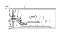
図12は、従来の技術による真空雰囲気内での位置決め装置と配管の概略図である。高真空に保たれた真空チャンバ1内にある位置決め対象物2は、定盤4上にあるステージ3によって精密な位置決めがなされる。ステージ3は、気体や液体の供給および回収が必要なため、フランジ5および蛇腹構造の金属配管6を介して真空チャンバ1外側と接続されている。なお、図中の矢印はステージ3が可動する旨を示すものである。
【0004】
【発明が解決しようとする課題】
しかし、真空雰囲気内にある可動部への接続に金属配管を使用する場合、配管自体からの脱ガス・透過ガスがほとんどないという利点がある一方、下記の2つ大きな問題点がある。
▲1▼柔軟性が悪い(曲げ剛性が大きい)ため可動に対しての負荷抵抗が大きく、つまり配管を変形させる際の力がステージ3の外乱要因となり、位置決め精度に悪影響を与える。
▲2▼金属配管7の繰り返し変形によって金属疲労を招きやすく、耐久性に不安がある。
【0005】
特に、高精度なステージ3では、柔軟性に富む樹脂材料で構成された配管でさえ配管の引き回しによる非線形な力が位置決め精度に悪影響を与えると言われている。このため、金属配管の柔軟性の悪さは大きな問題となっており、真空雰囲気内で使用できる柔軟性の高い配管が強く求められている。また、金属配管のかわりに柔軟性の高い樹脂材料の配管への置き換えも考えられるが、樹脂材料は一般的に脱ガスおよび透過ガスの量が金属配管に比ベて非常に大きいため、そのままでは中高真空内での使用は難しい。
【0006】
本発明は、上記の問題点に鑑みてなされたものであり、真空雰囲気内で、配管が接続された可動部を移動させて該可動部に搭載された対象物を位置決めする位置決め装置において、可動部に接続する配管として、従来の金属配管よりも柔軟で、かつ耐久性に優れた配管を提供することを目的としている。さらに電気配線の脱ガスの影響をも防ぐ配管を提供することも目的としている。
【0007】
【課題を解決するための手段および作用】
上記目的を達成するため、本発明に係る第1の位置決め装置は、真空雰囲気内で、配管が接続された可動部を移動させて該可動部に搭載された対象物を位置決めする位置決め装置であって、前記配管は樹脂製の内部配管と、該内部配管の外周を覆う樹脂製の外側配管とで構成された2重配管からなり、該内側配管と該外側配管との間の空間の気体を排気する排気機構を備えることを特徴とする。
【0008】
本発明において、前記配管は、前記空間が真空に保たれることが好ましい。
また、前記配管は真空チャンバ内に配置されており、前記空間内の圧力は前記真空チャンバ内よりも高い圧力に保たれることが好ましい。
また、前記真空チャンバ内と前記空間内との圧力差は、前記内部配管内と前記空間内との圧力差よりも小さいことが好ましい。
また、前記内側配管は、ポリウレタン系またはポリオレフィン系の樹脂で構成されていることが好ましい。
また、前記内部配管は、前記外側配管よりも柔軟性が高い材料であることが好ましい。
また、前記外側配管は、フッ素系樹脂で構成されていることが好ましい。
そして、前記外側配管は、前記内部配管よりも肉厚が薄いことが好ましい。
さらに、前記外側配管は、その肉厚が10μm以上、100μm以下であることが好ましい。
また、前記内部配管は、前記可動部に気体または液体を供給および回収するために用いられることが好ましい。
また、前記内部配管は複数の配管を有し、前記可動部が移動したときに該内部配管が曲がる曲げ方向における剛性が小さくなるように一列に並べて配置されることが好ましい。
そして、前記可動部に接続された電気配線を備える場合、該電気配線は前記外側配管の内部に配置されることが好ましい。
さらに、前記内部配管および前記電気配線は、前記可動部が移動したときに該内部配管および前記電気配線が曲がる曲げ方向における剛性が小さくなるように一列に並べて配置されることが好ましい。
【0009】
本発明に係る第2の位置決め装置は、真空雰囲気内で、単数または複数の電気配線が接続された可動部を移動させて該可動部に搭載された対象物を位置決めする位置決め装置であって、該電気配線の外周を覆う樹脂製の外側配管と、該電気配線と該外側配管との間の空間の気体を排気する排気機構とを有することを特徴とする。
【0010】
さらに、前記電気配線は、前記可動部が移動したときに該電気配線が曲がる曲げ方向における剛性が小さくなるように一列に並べて配置されることが好ましい。
【0011】
本発明の電子ビーム描画装置は、前記位置決め装置を有することができる。
本発明の露光装置は、前記位置決め装置を有することができる。
【0012】
本発明の露光装置による半導体デバイス製造方法は、前記電子ビーム描画装置または露光装置を含む各種プロセス用の製造装置群を半導体製造工場に設置する工程と、該製造装置群を用いて複数のプロセスによって半導体デバイスを製造する工程とを有することができる。
【0018】
【実施例】
次に、本発明の実施例について図面を用いて詳細に説明する。なお、本発明はこれらの実施例に限定されるものではない。
<第1の実施例>
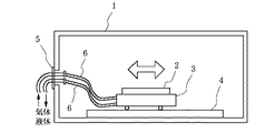
図1は、第1の実施例に係る真空雰囲気内に構成される位置決め装置を示す要部該略図であり、本発明を最もよく表す図である。
図中、1は内部が真空雰囲気に制御された真空チャンバである。真空チャンバ1には、不図示の真空ポンプが設けられており、真空チャンバ1内部の気体は真空ポンプによって排出され、真空チャンバ内部が真空雰囲気に制御される。
【0019】
3はステージであって、基準面を有する定盤4上を不図示の駆動機構によって移動可能である。位置決め対象物2は、ステージ3上に設けられた不図示のチャックにより保持されている。
ステージ3は、定盤4上に支持機構10によって非接触で支持されている。
【0020】
支持機構10について、図2を用いて説明を行う。なお、図2において、前述の図1と同じ要素については、同じ符号を付している。
支持機構10は、エアパッド11と、ラビリンス隔壁13を有する。エアパッド11は、ステージ3に設けられ、吸気用配管から供給されるエアを対向する定盤に向けて噴出している。このエアパッド11から噴出するエアにより、ステージ3は、定盤4上に非接触で支持されることになる。
【0021】
ここで、真空チャンバ1内にエアパッド11から噴出されるエアが漏洩することは望ましくない。そこで、エアパッド11を取り囲むように複数の隔壁を有するラビリンス隔壁13を設け、該隔壁13間に排気口を設けて強制排気を行うことにより、エアパッド11からのエアが真空チャンバ1に漏洩するのを防いでいる。
【0022】
すなわち、支持機構10によってステージ3を支持するために、ウテージ3には、吸気用配管と排気用配管が連結されている。
【0023】
また、ステージ3を駆動する駆動機構は、ステージ3を駆動する際に発熱を起こす。そこで、駆動機構を温調するための温調気体または温調液を発熱部に供給し、熱を回収した温調気体または温調液を回収する必要がある。そのため、ステージ3には、温調気体または温調液を供給および回収するための配管が連結されている。
【0024】
このように、ステージ3には、気体または液体を供給または排出するための各種の配管が施されている。そして、ステージ3に供給または排出される気体や液体は、真空チャンバ外部との間で循環されている。一方、ステージ3を高精度に位置決めするためには、配管による外乱は極力除去する必要がある。そのため、配管7には柔軟性の高い樹脂配管を用い、真空チャンバ1に設けられたフランジ5を介して気体・液体をステージ3に供給している。
【0025】
一般に、樹脂配管は、配管表面から構成材料等が真空雰囲気に放出される 「脱ガス」 や配管内の気体・液体が配管外側にしみ出る「透過」という現象が金属配管に比べて非常に大きい。配管の使用量によっては、それらのガスによって、真空チャンバの真空度が所望のレベルまであがらないことがある。材料によっては脱ガス量は問題にならないことも多いが、特に配管に圧力の高い気体・液体を流すと透過の量が非常に大きいため、真空チャンバ内の真空度に悪影響を与えることが多い。この対策として、ガス透過量は、配管内と雰囲気との圧力差に比例し、配管の肉厚に反比例する傾向にあることを利用して、透過量を少なくするために配管の肉厚を大きくすればよい。しかし、実際に樹脂配管を用いる際は、柔軟性が最大の理由であるため、肉厚を大きくすることはその利点を損ねる方向になってしまう。
【0026】
そこで、本実施例では、樹脂配管7からの脱ガス・透過ガスが真空チャンバ1内の雰囲気に影響を与えないよう、樹脂配管7の外側を肉厚の小さなフッ素樹脂の配管8で気密的に覆い、脱ガス・透過ガスの漏れを防いでいる。図2および図3にその詳細を示す。図2は1つの配管に対してのシール構造であり、図3は複数の配管に対するシール構造である。これらの図から分かるように、本実施例の真空配管は、2重配管の構成となっており、内側配管7は外側配管8にシールされて真空チャンバ1内の雰囲気にさらされない構造としている。さらに、図1のように、内側配管7と外側配管8との間の空間(気密的な空間)は、フランジ5を介して真空排気手段である真空ポンプにつながっていて、低真空に保たれている。
【0027】
上記した真空ポンプは、脱ガス・透過ガスの影響が真空チャンバ1内に影響を与えないように、真空チャンバ1内の真空度を保つ真空ポンプとはさらに別の真空ポンプであることを付け加えておく。また、真空チャンバ1内の真空度を保つ真空ポンプは、高真空にひけるが高価で取り扱いが面倒なターボ分子ポンプを用いることが多い。しかし、本実施例の真空配管に接続される真空ポンプは、低真空かつ低排気速度で引ければいいので、安価で取り扱いの容易なスクロールポンプ等で構わない。
【0028】
上記の構成等にすることによって、内側配管7からの脱ガス・透過ガスは真空チャンバ1内に漏れることがない。つまり、内側配管7は、当然多くの脱ガス・透過ガスを放出するが、それらのガスは真空ポンプによって回収される。また、真空ポンプによって内側配管7と外側配管8との間の気密的な空間は適当な低真空に保たれているため、外側配管8の内外での圧力差はほぼ0と考えられる。例えば、真空チャンバ1内の真空度が10-6[Pa]の高真空であり、内側配管7と外側配管8との間の空間が1[Pa]の低真空であっても、圧力差はほぼ1[Pa]と非常に小さい。そのため、外側配管8から真空チャンバ1内への透過ガスはほとんど0になる。また、外側配管8にかかる圧力差が非常に小さいことから、外側配管8は強度的な観点より非常に肉厚を薄くでき、つまり柔軟性を確保できる利点がある。しかし、外側配管8の脱ガスは、そのまま真空チャンバ1内に放出されるため、外側配管8の材料は脱ガスの少ない材料を選定しなくてはならない。
【0029】
以上のことから、本実施例では内側配管7は脱ガス・透過ガスをあまり気にしなくてもよいことから、柔軟性を優先してポリウレタン系やポリオレフィン系樹脂の配管を用いている。そして、外側配管8は、脱ガスの少なさを優先してフッ素系樹脂を用いて、さらに柔軟性を確保するために肉厚は50μmと非常に薄くしている。外側配管8の肉厚は、10μm〜100μm程度が位置決めに必要な柔軟性を確保でき、かつ外側配管8としての強度も十分に保たれる値である。また、脱ガスの少ない樹脂として、他にもポリイミド系樹脂等も挙げられ、所望する真空度と真空ポンプおよび材料の脱ガス量を考慮して、ある程度選定することが可能である。
【0030】
ここまで樹脂配管の柔軟性を利点として述べてきたが、樹脂配管で構成するもう1つの理由として、金属配管に比べて繰り返し変形に対して強く、よって耐久性に関する信頼性は格段に増すことが期待できることが挙げられる。繰り返し変形に強いということは、▲1▼もともと真空チャンバ内の装置はメンテナンスが困難で部品の交換は最小限にとどめたい場合が多いこと、▲2▼特に可動部が大きなストロークで頻繁に可動を繰り返す場合には耐久性の要求が大きいこと、等の要求に応えることになる。
【0031】
また、2重配管にした利点として、脱ガス・透過ガスの影響抑制だけでなく、真空配管としての信頼性向上も挙げられる。通常、高真空中に突然配管に亀裂等ができたりすると、配管を通る気体・液体が真空チャンバ1内に漏れ、真空チャンバ1内真空度が急激に低真空に落ちてしまう。このとき、中高真空でしか使用できないターボ分子ポンプや油拡散ポンプ等が破損してチャンバシステム全体の被害が甚大になる可能性がある。しかし、本発明の構成によると内側配管7および外側配管8が同時にリークしなければ、真空チャンバ1内に流入することはない。通常は、いずれか一方の配管が先に劣化すると考えられるが、内側配管7のみがリークすると内側配管7と外側配管8との間の気密的な空間の圧力があがる。それによって、外側配管8の透過ガス量が増え、真空チャンバ内の圧力があがる。しかし、外側配管8によってある程度リークガスがシールされていることを考えると、直接リークする場合に比べるとゆっくりとした圧力変化であることが予想される。従って、リークが発生した後すぐに適切な対処をとれば、チャンバシステムの被害を最小限に抑えることができる。また、外側配管8のみがリークした場合は、真空チャンバ1内の真空度は若干悪くなるが、真空ポンプおよびチャンバシステムに被害を与える程ではない場合がほとんどである。
【0032】
電子ビーム描画装置では、真空雰囲気内でウエハに電子ビームを照射するため、上記の配管を施したウエハステージを電子ビーム描画装置に搭載することが望ましい。
【0033】
また、上述の実施形態では、チャンバ1内は、真空雰囲気に制御されていたが、これに限られるものではない。チャンバ1内が、不活性ガス雰囲気等の所定のガス雰囲気に制御され、樹脂配管からの脱ガス等が問題となるようであれば、上述の実施形態による配管を利用することができることは、言うまでもない。そのため、例えば、窒素雰囲気やヘリウム雰囲気でウエハステージを制御する必要がある露光装置に用いてもよい。このような露光装置としては、例えば、F2レーザやArレーザを光源とする露光装置がある。
【0034】
ここで、図3のような複数の内側配管7を外側配管8内に構成した例について説明する。図3の様に複数の配管を必要とする場合には、本実施例では複数の内側配管7をまとめて外側配管8で覆い、さらにその内側配管7は可動部が可動する際に曲がる方向の曲げ剛性が小さくなるように配管軸方向の断面に関して1次元方向に並べてある。このように、内側配管7をまとめることにより、外側配管8の数を減らすことができる。そのため、外側配管8の脱ガスを少なくし、また外側配管8の曲げ剛性は数が減った分、小さくすることができた。また、内側配管7の配列をこのように工夫することにより、内側配管7全体の曲げ剛性を減らせ、配管全体の曲げ剛性を小さくすることができている。
【0035】
<第2の実施例>
図4は、本発明の一実施例に係る真空シール構造を電気配線に応用した一例である。一般に、電気配線においても、配線の被服部からの脱ガスを少なくするためフッ素系樹脂の被服線を用いることが多い。しかし、フッ素系樹脂の被服は、一般の被服に比べ柔軟性に劣り、可動部への接続には配管同様、あまり適してない。そこで、柔軟性を保ちながら脱ガスの少ない電気配線9を構成するために、電気配線9を肉厚の薄い (数十μm) フッ素系樹脂の外側配管8内に通し、外側配管8内はポンプで低真空に保つ構成をとっている。これにより、電気配線9自体は、脱ガスを気にせずビニール被服線等の柔軟なものを用いても、脱ガスは高真空雰囲気に影響を与えない。これは、第1の実施例と同様、圧力差がほぼ0なので、外側配管8内外での透過ガスはほとんどないことに基づく。また、外側配管8に用いるフッ素系樹脂は肉厚が薄いため柔軟性を確保でき、総合的にみても従来のフッ素系樹脂被服の電気配線9よりも格段に柔軟になっている。
【0036】
また、真空内の可動部が気体・液体の内側配管7と電気配線9の両方の接続を要する場合には、図5の様にフッ素系樹脂の外側配管8内に両方を配置すれば、可動部の引き回しがシンプルになる。ここで、図5は、真空雰囲気内の可動部に内側配管と電気配線の両方の接続を要する場合、複数配管および複数配線を同時に真空シール構造に適用した配管構造を示す図である。
【0037】
また、図4および図5においても第1の実施例と同様に、可動に対して曲がる方向の配管全体の曲げ剛性を小さくするように電気配線9および内側配管7を1次元的に配置している。
【0038】
<半導体生産システムの実施例>
次に、上記説明した露光装置を利用した半導体等のデバイス(ICやLSI等の半導体チップ、液晶パネル、CCD、薄膜磁気ヘッド、マイクロマシン等)の生産システムの例を説明する。これは、半導体製造工場に設置された製造装置のトラブル対応や定期メンテナンス、若しくはソフトウェア提供等の保守サービスを、製造工場外のコンピュータネットワーク等を利用して行うものである。
【0039】
図7は、全体システムをある角度から切り出して表現したものである。図中、101は半導体デバイスの製造装置を提供するベンダ(装置供給メーカ)の事業所である。製造装置の実例として、半導体製造工場で使用する各種プロセス用の半導体製造装置、例えば、前工程用機器(露光装置、レジスト処理装置、エッチング装置等のリソグラフィ装置、熱処理装置、成膜装置、平坦化装置等)や後工程用機器(組立て装置、検査装置等)を想定している。事業所101内には、製造装置の保守データベースを提供するホスト管理システム108、複数の操作端末コンピュータ110、これらを結んでイントラネット等を構築するローカルエリアネットワーク(LAN)109を備える。ホスト管理システム108は、LAN109を事業所の外部ネットワークであるインターネット105に接続するためのゲートウェイと、外部からのアクセスを制限するセキュリティ機能を備える。
【0040】
一方、102〜104は、製造装置のユーザとしての半導体製造メーカの製造工場である。製造工場102〜104は、互いに異なるメーカに属する工場であってもよいし、同一のメーカに属する工場(例えば、前工程用の工場、後工程用の工場等)であってもよい。各工場102〜104内には、夫々、複数の製造装置106と、それらを結んでイントラネット等を構築するローカルエリアネットワーク(LAN)111と、各製造装置106の稼動状況を監視する監視装置としてホスト管理システム107とが設けられている。各工場102〜104に設けられたホスト管理システム107は、各工場内のLAN111を工場の外部ネットワークであるインターネット105に接続するためのゲートウェイを備える。これにより各工場のLAN111からインターネット105を介してベンダ101側のホスト管理システム108にアクセスが可能となり、ホスト管理システム108のセキュリティ機能によって限られたユーザだけがアクセスが許可となっている。具体的には、インターネット105を介して、各製造装置106の稼動状況を示すステータス情報(例えば、トラブルが発生した製造装置の症状)を工場側からベンダ側に通知する他、その通知に対応する応答情報(例えば、トラブルに対する対処方法を指示する情報、対処用のソフトウェアやデータ)や、最新のソフトウェア、ヘルプ情報等の保守情報をベンダ側から受け取ることができる。各工場102〜104とベンダ101との間のデータ通信および各工場内のLAN111でのデータ通信には、インターネットで一般的に使用されている通信プロトコル(TCP/IP)が使用される。なお、工場外の外部ネットワークとしてインターネットを利用する代わりに、第三者からのアクセスができずにセキュリティの高い専用線ネットワーク(ISDN等)を利用することもできる。また、ホスト管理システムはベンダが提供するものに限らずユーザがデータベースを構築して外部ネットワーク上に置き、ユーザの複数の工場から該データベースへのアクセスを許可するようにしてもよい。
【0041】
さて、図8は、本実施形態の全体システムを図7とは別の角度から切り出して表現した概念図である。先の例では、それぞれが製造装置を備えた複数のユーザ工場と、該製造装置のベンダの管理システムとを外部ネットワークで接続して、該外部ネットワークを介して各工場の生産管理や少なくとも1台の製造装置の情報をデータ通信するものであった。これに対し本例は、複数のベンダの製造装置を備えた工場と、該複数の製造装置のそれぞれのベンダの管理システムとを工場外の外部ネットワークで接続して、各製造装置の保守情報をデータ通信するものである。図中、201は製造装置ユーザ(半導体デバイス製造メーカ)の製造工場であり、工場の製造ラインには各種プロセスを行う製造装置、ここでは例として露光装置202、レジスト処理装置203、成膜処理装置204が導入されている。なお、図8では、製造工場201は1つだけ描いているが、実際は複数の工場が同様にネットワーク化されている。工場内の各装置はLAN206で接続されてイントラネット等を構成し、ホスト管理システム205で製造ラインの稼動管理がされている。一方、露光装置メーカ210、レジスト処理装置メーカ220、成膜装置メーカ230等、ベンダ(装置供給メーカ)の各事業所には、それぞれ供給した機器の遠隔保守を行うためのホスト管理システム211,221,231を備え、これらは上述したように保守データベースと外部ネットワークのゲートウェイを備える。ユーザの製造工場内の各装置を管理するホスト管理システム205と、各装置のベンダの管理システム211,221,231とは、外部ネットワーク200であるインターネット若しくは専用線ネットワークによって接続されている。このシステムにおいて、製造ラインの一連の製造機器の中のどれかにトラブルが起きると、製造ラインの稼動が休止してしまうが、トラブルが起きた機器のベンダからインターネット200を介した遠隔保守を受けることで迅速な対応が可能で、製造ラインの休止を最小限に抑えることができる。
【0042】
半導体製造工場に設置された各製造装置はそれぞれ、ディスプレイと、ネットワークインタフェースと、記憶装置にストアされたネットワークアクセス用ソフトウェアならびに装置動作用のソフトウェアを実行するコンピュータを備える。記憶装置としては内蔵メモリやハードディスク、若しくはネットワークファイルサーバ等である。上記ネットワークアクセス用ソフトウェアは、専用又は汎用のウェブブラウザを含み、例えば図9に一例を示す様な画面のユーザインタフェースをディスプレイ上に提供する。各工場で製造装置を管理するオペレータは、画面を参照しながら、製造装置の機種401、シリアルナンバー402、トラブルの件名403、発生日404、緊急度405、症状406、対処法407、経過408等の情報を画面上の入力項目に入力する。入力された情報はインターネットを介して保守データベースに送信され、その結果の適切な保守情報が保守データベースから返信されディスプレイ上に提示される。また、ウェブブラウザが提供するユーザインタフェースは、さらに図示のごとくハイパーリンク機能410,411,412を実現し、オペレータは各項目の更に詳細な情報にアクセスしたり、ベンダが提供するソフトウェアライブラリから製造装置に使用する最新バージョンのソフトウェアを引出したり、工場のオペレータの参考に供する操作ガイド(ヘルプ情報)を引出したりすることができる。ここで、保守データベースが提供する保守情報には、上記説明した本発明に関する情報も含まれ、また前記ソフトウェアライブラリは本発明を実現するための最新のソフトウェアも提供する。
【0043】
次に、上記説明した生産システムを利用した半導体デバイスの製造プロセスを説明する。図10は、半導体デバイスの全体的な製造プロセスのフローを示す。ステップ1(回路設計)では半導体デバイスの回路設計を行う。ステップ2(マスク製作)では設計した回路パターンを形成したマスクを製作する。一方、ステップ3(ウエハ製造)ではシリコン等の材料を用いてウエハを製造する。ステップ4(ウエハプロセス)は前工程と呼ばれ、上記用意したマスクとウエハを用いて、リソグラフィ技術によってウエハ上に実際の回路を形成する。次のステップ5(組み立て)は後工程と呼ばれ、ステップ4によって作製されたウエハを用いて半導体チップ化する工程であり、アッセンブリ工程(ダイシング、ボンディング)、パッケージング工程(チップ封入)等の組立て工程を含む。ステップ6(検査)ではステップ5で作製された半導体デバイスの動作確認テスト、耐久性テスト等の検査を行う。こうした工程を経て半導体デバイスが完成し、これを出荷(ステップ7)する。前工程と後工程はそれぞれ専用の別の工場で行い、これらの工場毎に上記説明した遠隔保守システムによって保守がなされる。また、前工程工場と後工程工場との間でも、インターネットまたは専用線ネットワークを介して生産管理や装置保守のための情報がデータ通信される。
【0044】
図11は、上記ウエハプロセスの詳細なフローを示す。ステップ11(酸化)ではウエハの表面を酸化させる。ステップ12(CVD)ではウエハ表面に絶縁膜を成膜する。ステップ13(電極形成)ではウエハ上に電極を蒸着によって形成する。ステップ14(イオン打込み)ではウエハにイオンを打ち込む。ステップ15(レジスト処理)ではウエハに感光剤を塗布する。ステップ16(露光)では上記説明した露光装置によってマスクの回路パターンをウエハに焼付露光する。ステップ17(現像)では露光したウエハを現像する。ステップ18(エッチング)では現像したレジスト像以外の部分を削り取る。ステップ19(レジスト剥離)ではエッチングが済んで不要となったレジストを取り除く。これらのステップを繰り返し行うことによって、ウエハ上に多重に回路パターンを形成する。各工程で使用する製造機器は上記説明した遠隔保守システムによって保守がなされているので、トラブルを未然に防ぐと共に、もしトラブルが発生しても迅速な復旧が可能で、従来に比べて半導体デバイスの生産性を向上させることができる。
【0045】
【発明の効果】
本発明によれば、配管自体からの脱ガス・透過ガスの影響を抑えながらも柔軟性に富み、繰り返し変形に対する耐久性が高く、位置決め装置における可動部への接続に適した配管を提供できる。
【0046】
そして、外側配管に脱ガスの少ない樹脂材料を用いると、さらに配管全体からの脱ガスを少なくすることができ、真空チャンバ内部への真空度への悪影響が小さくなり、また内側配管に柔軟性の高い樹脂材料を用いることで配管全体の柔軟性が増す。さらに、外側配管の肉厚は0.1mm程度以下の薄い肉厚にすることで、配管全体の柔軟性を保つことが可能になる。
【0047】
また、内側配管の替わりに電気配線で上記のような構成をとっても、脱ガスの影響を防ぐことが可能となる。そして、2つ以上の内側配管および/または電気配線等を組み合わせた可動部への引き回し部材全体を1つの外側配管によって気密的に覆えば、可動部(ステージ)への引き回しが構成上シンプルになる。その際、内側配管や電気配線等は、軸方向の断面に関して1次元方向に並べると配管(内側配管の一部または全部の替わりに電気配線を構成した場合を含む)の曲げ剛性の小さな曲げ方向ができるため有効である。
【0048】
真空雰囲気内の位置決め装置を構成する際に、以上述べてきた配管(内側配管の一部または全部の替わりに電気配線を構成した場合を含む)を可動部(ステージ)への接続に用いることで、可動に対する非線形な負荷が少なくなり、これにより位置決め精度をよくすることができる。
【図面の簡単な説明】
【図1】 本発明の一実施例に係る真空雰囲気内に構成される位置決め装置を示す要部該略図である。
【図2】 図1の支持機構10を説明する図である。
【図3】 第1の実施例に係る単数配管である樹脂配管の外側を肉厚の小さなフッ素樹脂の配管で気密的に覆った場合の配管構造を示す図である。
【図4】 第1の実施例に係る複数配管である樹脂配管の外側を肉厚の小さなフッ素樹脂の配管で気密的に覆った場合の配管構造を示す図である。
【図5】 第2の実施例に係る真空シール構造を電気配線に応用した配管構造を示す図である。
【図6】 真空雰囲気内の可動部に内側配管と電気配線の両方の接続を要する場合、複数配管および複数配線を同時に真空シール構造に適用した配管構造を示す図である。
【図7】 本発明の一実施例に係る露光装置を含む半導体デバイスの生産システムをある角度から見た概念図である。
【図8】 本発明の一実施例に係る露光装置を含む半導体デバイスの生産システムを別の角度から見た概念図である。
【図9】 本発明の一実施例に係る露光装置を含む半導体デバイスの生産システムにおけるユーザインタフェースの具体例を示す図である。
【図10】 本発明の一実施例に係る露光装置によるデバイスの製造プロセスのフローを説明する図である。
【図11】 本発明の一実施例に係る露光装置によるウエハプロセスを説明する図である。
【図12】 従来の技術による真空雰囲気内での位置決め装置と配管の概略図である。
【符号の説明】
1:真空チャンバ、2:位置決め対象物、3:ステージ、4:定盤、5:フランジ、6:金属配管、7:内側配管(樹脂配管)、8:外側配管(樹脂配管)、9:電気配線、10:支持機構、11:エアパッド、13:ラビリンス隔壁、101:ベンダの事業所、102,103,104:製造工場、105:インターネット、106:製造装置、107:工場のホスト管理システム、108:ベンダ側のホスト管理システム、109:ベンダ側のローカルエリアネットワーク(LAN)、110:操作端末コンピュータ、1111:工場のローカルエリアネットワーク(LAN)、200:外部ネットワーク、201:製造装置ユーザの製造工場、202:露光装置、203:レジスト処理装置、204:成膜処理装置、205:工場のホスト管理システム、206:工場のローカルエリアネットワーク(LAN)、210:露光装置メーカ、211:露光装置メーカの事業所のホスト管理システム、220:レジスト処理装置メーカ、221:レジスト処理装置メーカの事業所のホスト管理システム、230:成膜装置メーカ、231:成膜装置メーカの事業所のホスト管理システム、401:製造装置の機種、402:シリアルナンバー、403:トラブルの件名、404:発生日、405:緊急度、406:症状、407:対処法、408:経過、410,411,412:ハイパーリンク機能。[0001]
BACKGROUND OF THE INVENTION
The present invention, in a vacuum atmosphere, the pipe moves the movable portion which is connected relates to a positioner for positioning the onboard object to the movable section. More particularly , the present invention relates to a highly accurate positioning apparatus in a medium-high vacuum atmosphere that prevents adverse effects on the degree of vacuum in a vacuum chamber from degassing / permeating gas or the like of piping connected to a movable part.
[0002]
[Prior art]
Conventionally, when a gas or liquid is allowed to enter and exit between the inside of the medium / high vacuum atmosphere and the outside of the vacuum chamber, in order to avoid degassing from the piping and adverse effects on the degree of vacuum in the vacuum chamber due to permeated gas, I use it. Furthermore, regarding the connection to the movable part in the vacuum atmosphere, in order to ensure the flexibility of the pipe, it is common to use a metal pipe having a bellows structure called a flexible pipe.
[0003]
FIG. 12 is a schematic view of a positioning device and piping in a vacuum atmosphere according to the prior art. The positioning object 2 in the
[0004]
[Problems to be solved by the invention]
However, when a metal pipe is used for connection to a movable part in a vacuum atmosphere, there is an advantage that there is almost no degassing / permeating gas from the pipe itself, but there are the following two major problems.
(1) Since the flexibility is poor (the bending rigidity is large), the load resistance against movement is large, that is, the force for deforming the piping becomes a disturbance factor of the
(2) Metal fatigue is easily caused by repeated deformation of the
[0005]
In particular, in the high-
[0006]
The present invention has been made in view of the above problems, and in a positioning apparatus that moves a movable part to which a pipe is connected in a vacuum atmosphere to position an object mounted on the movable part. and a pipe which connects to the part, and its object is to provide a than conventional metal piping, flexible, and durable piping. It is another object of the present invention to provide piping that prevents the influence of degassing of electrical wiring.
[0007]
[Means and Actions for Solving the Problems]
In order to achieve the above object, a first positioning apparatus according to the present invention is a positioning apparatus that moves a movable part to which a pipe is connected in a vacuum atmosphere to position an object mounted on the movable part. Te, the piping and the piping made of resin, made double pipe constituted by a resin outer pipe covering the outer periphery of the internal pipe, a gas space between the inner pipe and the outer pipe an exhaust mechanism for exhausting characterized Rukoto.
[0008]
In the present invention, the pipe, it is preferable that the space is maintained under vacuum.
Moreover, it is preferable that the said piping is arrange | positioned in a vacuum chamber and the pressure in the said space is maintained at a pressure higher than the inside of the said vacuum chamber.
The pressure difference between the vacuum chamber and the space is preferably smaller than the pressure difference between the internal pipe and the space.
Further, the inner pipe is preferably formed of a polyurethane or polyolefin resin.
The internal pipe is preferably made of a material having higher flexibility than the outer pipe.
Further, the outer pipe is preferably formed of a fluorine-based resin.
The outer pipe is preferably thinner than the inner pipe.
Further, the outer pipe preferably has a wall thickness of 10 μm or more and 100 μm or less.
Moreover, it is preferable that the said internal piping is used in order to supply and collect | recover gas or a liquid to the said movable part.
In addition, it is preferable that the internal pipe has a plurality of pipes and is arranged in a line so that rigidity in a bending direction in which the internal pipe is bent when the movable portion moves is reduced.
And when providing the electrical wiring connected to the said movable part, it is preferable that this electrical wiring is arrange | positioned inside the said outer side piping.
Further, it is preferable that the internal pipe and the electric wiring are arranged in a line so that rigidity in a bending direction in which the internal pipe and the electric wiring are bent when the movable portion moves is reduced.
[0009]
A second positioning device according to the present invention is a positioning device that moves a movable part to which one or a plurality of electrical wirings are connected in a vacuum atmosphere to position an object mounted on the movable part, and having an outer pipe made of resin covering the outer periphery of the electric sign line, and an exhaust mechanism for exhausting the gas in the space between the electric wire and the outer pipe.
[0010]
Furthermore, before Symbol electrical wiring, the rigidity of definitive bending direction electric sign line is bent when the movable portion is moved is disposed in a row to be smaller so it is preferable.
[0011]
The electron beam drawing apparatus of the present invention can have the positioning device.
The exposure apparatus of the present invention can have the positioning device .
[0012]
A semiconductor device manufacturing method using an exposure apparatus according to the present invention includes a step of installing a manufacturing apparatus group for various processes including the electron beam lithography apparatus or the exposure apparatus in a semiconductor manufacturing factory, and a plurality of processes using the manufacturing apparatus group. A step of manufacturing a semiconductor device .
[0018]
【Example】
Next, embodiments of the present invention will be described in detail with reference to the drawings. The present invention is not limited to these examples.
<First embodiment>
FIG. 1 is a schematic view showing the main part of a positioning device configured in a vacuum atmosphere according to a first embodiment, and best represents the present invention.
In the figure,
[0019]
A
The
[0020]
The
The
[0021]
Here, it is not desirable that the air ejected from the
[0022]
That is, in order to support the
[0023]
The drive mechanism that drives the
[0024]
Thus, the
[0025]
In general, resin pipes have a significantly larger phenomenon of “degassing” in which constituent materials are released from the pipe surface to the vacuum atmosphere and “permeation” in which gas and liquid in the pipe ooze out to the outside of the pipe. . Depending on the amount of piping used, these gases may not increase the vacuum level of the vacuum chamber to a desired level. Depending on the material, the amount of degassing often does not cause a problem, but especially when a gas or liquid having a high pressure is passed through the pipe, the amount of permeation is very large, and thus the degree of vacuum in the vacuum chamber is often adversely affected. As a countermeasure, the gas permeation amount is proportional to the pressure difference between the pipe and the atmosphere, and tends to be inversely proportional to the pipe wall thickness. do it. However, when resin pipes are actually used, the greatest reason is flexibility, so increasing the wall thickness tends to impair the advantages.
[0026]
Therefore, in this embodiment, the outer side of the
[0027]
The above-described vacuum pump is additionally a vacuum pump different from the vacuum pump that maintains the degree of vacuum in the
[0028]
By adopting the above-described configuration or the like, the degassed / permeated gas from the
[0029]
From the above, in this embodiment, the
[0030]
Up to this point, the flexibility of resin piping has been described as an advantage. Another reason for using resin piping is that it is more resistant to repeated deformation than metal piping, so the reliability of durability can be greatly increased. What can be expected. The fact that it is resistant to repeated deformation is as follows: (1) The equipment in the vacuum chamber is inherently difficult to maintain and there are many cases where it is necessary to minimize the replacement of parts, and (2) the movable part is particularly movable with a large stroke. In the case of repetition, the demand for durability is large, and so on.
[0031]
Further, as an advantage of the double piping, not only the influence of degassing / permeating gas is suppressed, but also the reliability improvement as a vacuum piping is mentioned. Normally, if a pipe is suddenly cracked in a high vacuum, the gas / liquid passing through the pipe leaks into the
[0032]
In the electron beam drawing apparatus, it is desirable to mount the wafer stage provided with the above-described piping on the electron beam drawing apparatus in order to irradiate the wafer with an electron beam in a vacuum atmosphere.
[0033]
In the above-described embodiment, the inside of the
[0034]
Here, the example which comprised the some inner side piping 7 like FIG. 3 in the outer side piping 8 is demonstrated. When a plurality of pipes are required as shown in FIG. 3, in this embodiment, the plurality of
[0035]
<Second embodiment>
FIG. 4 is an example in which the vacuum seal structure according to one embodiment of the present invention is applied to electrical wiring. In general, in order to reduce the outgassing from the covered part of the wiring, the wiring line of the fluorine-based resin is often used in the electric wiring. However, fluororesin clothing is less flexible than ordinary clothing and is not very suitable for connection to moving parts, as is the case with piping. Therefore, in order to configure the
[0036]
Further, when the movable part in the vacuum needs to connect both the gas / liquid
[0037]
4 and 5, as in the first embodiment, the
[0038]
<Example of semiconductor production system>
Next, an example of a production system for a device such as a semiconductor using the above-described exposure apparatus (a semiconductor chip such as an IC or LSI, a liquid crystal panel, a CCD, a thin film magnetic head, a micro machine, etc.) will be described. This is to perform maintenance services such as troubleshooting, periodic maintenance, or provision of software for a manufacturing apparatus installed in a semiconductor manufacturing factory using a computer network outside the manufacturing factory.
[0039]
FIG. 7 shows the whole system cut out from a certain angle. In the figure,
[0040]
On the other hand, 102 to 104 are manufacturing factories of semiconductor manufacturers as users of manufacturing apparatuses. The
[0041]
FIG. 8 is a conceptual diagram showing the overall system of this embodiment cut out from an angle different from that in FIG. In the above example, a plurality of user factories each equipped with a manufacturing device and a management system of a vendor of the manufacturing device are connected by an external network, and production control of each factory or at least one device is performed via the external network. The information of the manufacturing apparatus was data-communication. On the other hand, in this example, a factory equipped with a plurality of vendors' manufacturing devices and a management system of each vendor of the plurality of manufacturing devices are connected by an external network outside the factory, and maintenance information of each manufacturing device is obtained. Data communication. In the figure,
[0042]
Each manufacturing apparatus installed in the semiconductor manufacturing factory includes a display, a network interface, and a computer that executes network access software stored in a storage device and software for operating the apparatus. The storage device is a built-in memory, a hard disk, a network file server, or the like. The network access software includes a dedicated or general-purpose web browser, and provides, for example, a user interface having a screen as shown in FIG. 9 on the display. The operator who manages the manufacturing apparatus in each factory refers to the screen, and the
[0043]
Next, a semiconductor device manufacturing process using the above-described production system will be described. FIG. 10 shows the flow of the entire manufacturing process of the semiconductor device. In step 1 (circuit design), a semiconductor device circuit is designed. In step 2 (mask production), a mask on which the designed circuit pattern is formed is produced. On the other hand, in step 3 (wafer manufacture), a wafer is manufactured using a material such as silicon. Step 4 (wafer process) is called a pre-process, and an actual circuit is formed on the wafer by lithography using the prepared mask and wafer. The next step 5 (assembly) is called a post-process, and is a process for forming a semiconductor chip using the wafer produced in step 4, and is an assembly process (dicing, bonding), packaging process (chip encapsulation), etc. Process. In step 6 (inspection), the semiconductor device manufactured in
[0044]
FIG. 11 shows a detailed flow of the wafer process. In step 11 (oxidation), the wafer surface is oxidized. In step 12 (CVD), an insulating film is formed on the wafer surface. In step 13 (electrode formation), an electrode is formed on the wafer by vapor deposition. In step 14 (ion implantation), ions are implanted into the wafer. In step 15 (resist process), a photosensitive agent is applied to the wafer. In step 16 (exposure), the circuit pattern of the mask is printed onto the wafer by exposure using the exposure apparatus described above. In step 17 (development), the exposed wafer is developed. In step 18 (etching), portions other than the developed resist image are removed. In step 19 (resist stripping), unnecessary resist after etching is removed. By repeating these steps, multiple circuit patterns are formed on the wafer. Since the manufacturing equipment used in each process is maintained by the remote maintenance system described above, it is possible to prevent problems before they occur, and to recover quickly if a problem occurs. Productivity can be improved.
[0045]
【The invention's effect】
By the present invention lever, while suppressing the influence of degassing-permeate gas from the pipe itself flexible and high durability against repeated deformation, it is possible to provide a pipe suitable for connection to the movable part in the positioning device .
[0046]
If a resin material with less degassing is used for the outer pipe, degassing from the entire pipe can be further reduced, the adverse effect on the degree of vacuum inside the vacuum chamber is reduced, and the inner pipe is flexible. The use of a high resin material increases the flexibility of the entire pipe. Furthermore, the flexibility of the entire pipe can be maintained by setting the thickness of the outer pipe to a thin thickness of about 0.1 mm or less.
[0047]
Moreover, even if it takes the above-mentioned composition with electric wiring instead of inner piping, it becomes possible to prevent the influence of degassing. If the entire routing member to the movable part in which two or more inner pipes and / or electric wirings are combined is hermetically covered with one outer pipe, the routing to the movable part (stage) becomes simple in configuration. . At that time, the inner piping and electrical wiring, etc. are arranged in a one-dimensional direction with respect to the axial cross section, and the bending direction in which the bending rigidity of the piping (including the case where electric wiring is configured instead of part or all of the inner piping) is small. It is effective because it can.
[0048]
When constructing a positioning device in a vacuum atmosphere, the pipes described above (including cases where electrical wiring is constructed instead of part or all of the inner pipes) are used for connection to the movable part (stage). The non-linear load for the movement is reduced, thereby improving the positioning accuracy.
[Brief description of the drawings]
FIG. 1 is a schematic view showing a main part of a positioning device configured in a vacuum atmosphere according to an embodiment of the present invention.
FIG. 2 is a diagram illustrating a
FIG. 3 is a diagram showing a piping structure when the outside of a resin pipe, which is a single pipe according to the first embodiment, is airtightly covered with a thin fluororesin pipe.
FIG. 4 is a diagram showing a piping structure when the outer side of a resin pipe, which is a plurality of pipes, according to the first embodiment is hermetically covered with a small-thickness fluororesin pipe.
FIG. 5 is a view showing a piping structure in which the vacuum seal structure according to the second embodiment is applied to electric wiring.
FIG. 6 is a diagram showing a piping structure in which a plurality of piping and a plurality of wirings are simultaneously applied to a vacuum seal structure when both the inner piping and the electrical wiring are required to be connected to a movable part in a vacuum atmosphere.
FIG. 7 is a conceptual view of a semiconductor device production system including an exposure apparatus according to an embodiment of the present invention as seen from a certain angle.
FIG. 8 is a conceptual view of a semiconductor device production system including an exposure apparatus according to an embodiment of the present invention as seen from another angle.
FIG. 9 is a diagram showing a specific example of a user interface in a semiconductor device production system including an exposure apparatus according to an embodiment of the present invention.
FIG. 10 is a view for explaining the flow of a device manufacturing process by the exposure apparatus according to an embodiment of the present invention.
FIG. 11 is a view for explaining a wafer process by an exposure apparatus according to an embodiment of the present invention.
FIG. 12 is a schematic view of a positioning device and piping in a vacuum atmosphere according to the prior art.
[Explanation of symbols]
1: vacuum chamber, 2: object to be positioned, 3: stage, 4: surface plate, 5: flange, 6: metal piping, 7: inner piping (resin piping), 8: outer piping (resin piping), 9: electricity Wiring, 10: support mechanism, 11: air pad, 13: labyrinth partition, 101: vendor office, 102, 103, 104: manufacturing factory, 105: internet, 106: manufacturing equipment, 107: factory host management system, 108 : Vendor-side host management system, 109: Vendor-side local area network (LAN), 110: Operating terminal computer, 1111: Factory local area network (LAN), 200: External network, 201: Manufacturing apparatus user's manufacturing factory 202: exposure apparatus, 203: resist processing apparatus, 204: film formation processing apparatus, 205: factory Management system, 206: local area network (LAN) of the factory, 210: exposure apparatus manufacturer, 211: host management system of the exposure apparatus manufacturer, 220: resist processing apparatus manufacturer, 221: registration processing apparatus manufacturer Host management system, 230: film forming apparatus manufacturer, 231: host management system at the office of the film forming apparatus manufacturer, 401: type of manufacturing apparatus, 402: serial number, 403: subject of trouble, 404: date of occurrence, 405 : Urgency, 406: Symptom, 407: Countermeasure, 408: Progress, 410, 411, 412: Hyperlink function.
Claims (18)
前記配管は樹脂製の内部配管と、該内部配管の外周を覆う樹脂製の外側配管とで構成された2重配管からなり、
該内側配管と該外側配管との間の空間の気体を排気する排気機構を備えることを特徴とする位置決め装置。 In a vacuum atmosphere, a positioning device that moves a movable part connected to a pipe and positions an object mounted on the movable part,
The pipe comprises an inner pipe made of the resin, from the double pipe constituted by a resin outer pipe covering the outer periphery of the internal pipe,
Positioning device according to claim Rukoto an exhaust mechanism for exhausting the gas in the space between the inner pipe and the outer pipe.
該電気配線の外周を覆う樹脂製の外側配管と、該電気配線と該外側配管との間の空間の気体を排気する排気機構とを有することを特徴とする位置決め装置。 A positioning device for positioning a target object mounted on the movable part by moving a movable part to which one or more electrical wirings are connected in a vacuum atmosphere ,
A positioning apparatus comprising: an outer pipe made of resin that covers an outer periphery of the electric wiring; and an exhaust mechanism that exhausts gas in a space between the electric wiring and the outer pipe.
Priority Applications (3)
| Application Number | Priority Date | Filing Date | Title |
|---|---|---|---|
| JP2000112216A JP4383626B2 (en) | 2000-04-13 | 2000-04-13 | Positioning apparatus and exposure apparatus |
| US09/833,766 US6915179B2 (en) | 2000-04-13 | 2001-04-13 | Pipe structure, alignment apparatus, electron beam lithography apparatus, exposure apparatus, exposure apparatus maintenance method, semiconductor device manufacturing method, and semiconductor manufacturing factory |
| US11/050,746 US20050132962A1 (en) | 2000-04-13 | 2005-02-07 | Pipe structure, alignment apparatus, electron beam lithography apparatus, exposure apparatus, exposure apparatus maintenance method, semiconductor device manufacturing method, and semiconductor device manufacturing factory |
Applications Claiming Priority (1)
| Application Number | Priority Date | Filing Date | Title |
|---|---|---|---|
| JP2000112216A JP4383626B2 (en) | 2000-04-13 | 2000-04-13 | Positioning apparatus and exposure apparatus |
Publications (3)
| Publication Number | Publication Date |
|---|---|
| JP2001297967A JP2001297967A (en) | 2001-10-26 |
| JP2001297967A5 JP2001297967A5 (en) | 2007-05-31 |
| JP4383626B2 true JP4383626B2 (en) | 2009-12-16 |
Family
ID=18624424
Family Applications (1)
| Application Number | Title | Priority Date | Filing Date |
|---|---|---|---|
| JP2000112216A Expired - Fee Related JP4383626B2 (en) | 2000-04-13 | 2000-04-13 | Positioning apparatus and exposure apparatus |
Country Status (2)
| Country | Link |
|---|---|
| US (2) | US6915179B2 (en) |
| JP (1) | JP4383626B2 (en) |
Families Citing this family (41)
| Publication number | Priority date | Publication date | Assignee | Title |
|---|---|---|---|---|
| JP4535677B2 (en) * | 2000-10-17 | 2010-09-01 | ナノグラム・コーポレイション | Coating film production by reactive deposition |
| TW591342B (en) | 2000-11-30 | 2004-06-11 | Asml Netherlands Bv | Lithographic projection apparatus and integrated circuit manufacturing method using a lithographic projection apparatus |
| JP2004146492A (en) * | 2002-10-23 | 2004-05-20 | Canon Inc | Euv aligner |
| US7282821B2 (en) * | 2002-01-28 | 2007-10-16 | Canon Kabushiki Kaisha | Linear motor, stage apparatus, exposure apparatus, and device manufacturing apparatus |
| US6888143B2 (en) | 2002-03-09 | 2005-05-03 | Kimberly-Clark Worldwide, Inc. | Apparatus and method for inspecting pre-fastened articles |
| US7039999B2 (en) * | 2002-04-25 | 2006-05-09 | Tarr Adam L | Method for installation of semiconductor fabrication tools |
| US7551628B2 (en) * | 2002-05-03 | 2009-06-23 | Hewlett-Packard Development Company, L.P. | Wireless dongle with computing capability for equipment control and method of operation thereof |
| EP1418017A3 (en) * | 2002-08-29 | 2008-12-24 | Canon Kabushiki Kaisha | Positioning apparatus, charged particle beam exposure apparatus, and semiconductor device manufacturing method |
| JP2004266209A (en) * | 2003-03-04 | 2004-09-24 | Canon Inc | Exposing device and method for manufacturing the device |
| JP3748559B2 (en) * | 2003-06-30 | 2006-02-22 | キヤノン株式会社 | Stage apparatus, exposure apparatus, charged beam drawing apparatus, device manufacturing method, substrate potential measuring method, and electrostatic chuck |
| JP2005032818A (en) * | 2003-07-08 | 2005-02-03 | Canon Inc | Hydrostatic bearing, pointing device and aligner |
| JP3826118B2 (en) * | 2003-07-08 | 2006-09-27 | キヤノン株式会社 | Exposure equipment |
| JP2005033135A (en) * | 2003-07-11 | 2005-02-03 | Kobe Steel Ltd | Cleaning device for microstructure |
| JP4464097B2 (en) * | 2003-09-29 | 2010-05-19 | キヤノン株式会社 | Wiring structure and exposure apparatus |
| JP3894562B2 (en) | 2003-10-01 | 2007-03-22 | キヤノン株式会社 | Substrate adsorption apparatus, exposure apparatus, and device manufacturing method |
| JP3814598B2 (en) * | 2003-10-02 | 2006-08-30 | キヤノン株式会社 | Temperature adjustment apparatus, exposure apparatus, and device manufacturing method |
| US7034924B2 (en) * | 2004-01-12 | 2006-04-25 | Aslm Netherlands B.V. | Lithographic apparatus and device manufacturing method |
| JP4418699B2 (en) | 2004-03-24 | 2010-02-17 | キヤノン株式会社 | Exposure equipment |
| WO2006023595A2 (en) | 2004-08-18 | 2006-03-02 | New Way Machine Components, Inc. | Moving vacuum chamber stage with air bearing and differentially pumped grooves |
| JP2006156632A (en) * | 2004-11-29 | 2006-06-15 | Nikon Corp | Gas temperature control device, body tube, exposure device manufacturing method of device and gas temperature control method |
| DE102004059593B4 (en) * | 2004-12-10 | 2009-04-02 | Gabo Systemtechnik Gmbh | pipe Association |
| JP2006287014A (en) * | 2005-04-01 | 2006-10-19 | Canon Inc | Positioning apparatus and linear motor |
| WO2007023813A1 (en) * | 2005-08-23 | 2007-03-01 | Nikon Corporation | Exposure apparatus, exposure method, and device manufacturing method |
| JP4125315B2 (en) * | 2005-10-11 | 2008-07-30 | キヤノン株式会社 | Exposure apparatus and device manufacturing method |
| EP1843206B1 (en) * | 2006-04-06 | 2012-09-05 | ASML Netherlands B.V. | Lithographic apparatus and device manufacturing method |
| JP5318235B2 (en) * | 2006-05-26 | 2013-10-16 | キヤノン株式会社 | Stage apparatus, exposure apparatus, and device manufacturing method |
| JP5020662B2 (en) | 2006-05-26 | 2012-09-05 | キヤノン株式会社 | Stage apparatus, exposure apparatus, and device manufacturing method |
| JP4559532B2 (en) * | 2007-03-28 | 2010-10-06 | パイオニア株式会社 | Electron beam drawing apparatus and its stage mechanism |
| US9052616B2 (en) * | 2009-12-08 | 2015-06-09 | Asml Holding N.V. | Dual containment system having coaxial flexible tubes for transporting a fluid through a “rolling loop” cable duct |
| WO2013160021A1 (en) * | 2012-04-23 | 2013-10-31 | Asml Netherlands B.V. | Flexible conduit for fluid, lithographic apparatus, and method for manufacturing a device |
| JP6071425B2 (en) * | 2012-10-30 | 2017-02-01 | キヤノン株式会社 | Stage apparatus, lithography apparatus, and article manufacturing method |
| US9527107B2 (en) * | 2013-01-11 | 2016-12-27 | International Business Machines Corporation | Method and apparatus to apply material to a surface |
| US9437433B2 (en) * | 2014-02-03 | 2016-09-06 | Taiwan Semiconductor Manufacturing Co., Ltd | Method and apparatus for cooling wafer in ion implantation process |
| JP6505209B2 (en) * | 2014-09-05 | 2019-04-24 | ホワ キム,テ | Fume remover for semiconductor manufacturing chamber |
| US9484183B2 (en) * | 2014-09-10 | 2016-11-01 | Varian Semiconductor Equipment Associates, Inc. | Linkage conduit for vacuum chamber applications |
| DE102017109820B4 (en) | 2017-04-26 | 2024-03-28 | VON ARDENNE Asset GmbH & Co. KG | Vacuum chamber arrangement and its use |
| DE102017119841A1 (en) * | 2017-08-29 | 2019-02-28 | Labomatic Instruments Ag | hose assembly |
| WO2019096644A1 (en) * | 2017-11-14 | 2019-05-23 | Asml Netherlands B.V. | Object stage bearing for lithographic apparatus |
| KR102459089B1 (en) * | 2017-12-21 | 2022-10-27 | 삼성전자주식회사 | Semiconductor packaging apparatus and a method for manufacturing semiconductor devices using the same |
| JP7273665B2 (en) | 2019-09-11 | 2023-05-15 | 東京エレクトロン株式会社 | Heat medium circulation system and substrate processing equipment |
| IL295061A (en) * | 2020-02-18 | 2022-09-01 | Asml Netherlands Bv | Fluid transfer system in a charged particle system |
Family Cites Families (22)
| Publication number | Priority date | Publication date | Assignee | Title |
|---|---|---|---|---|
| GB1302909A (en) * | 1969-05-02 | 1973-01-10 | ||
| US4368219A (en) * | 1980-06-13 | 1983-01-11 | Sumitomo Light Metal Industries Ltd. | Method and apparatus for coating the inner surface of long tubes of small diameter |
| JPS57204547A (en) * | 1981-06-12 | 1982-12-15 | Hitachi Ltd | Exposing method |
| US4528451A (en) * | 1982-10-19 | 1985-07-09 | Varian Associates, Inc. | Gap control system for localized vacuum processing |
| DE3620969A1 (en) * | 1985-06-24 | 1987-01-02 | Canon Kk | PRECISION FEED MECHANISM |
| JPS6398413A (en) * | 1986-10-15 | 1988-04-28 | Smc Corp | Double pipe and its continuous manufacture |
| US4993696A (en) * | 1986-12-01 | 1991-02-19 | Canon Kabushiki Kaisha | Movable stage mechanism |
| JPH05311412A (en) * | 1992-05-11 | 1993-11-22 | Toppan Printing Co Ltd | Production of feed material for vapor deposition and transparent barrier film |
| US5304073A (en) * | 1992-06-05 | 1994-04-19 | Carr-Griff, Inc. | Electrical connector and pump assembly utilizing same |
| US5829483A (en) * | 1992-10-30 | 1998-11-03 | Toyoda Gosei Co., Ltd. | Hose |
| CA2133665C (en) * | 1993-02-05 | 1997-01-14 | Jean-Claude Douchet | Multilayer plastic duct |
| KR100267617B1 (en) * | 1993-04-23 | 2000-10-16 | 히가시 데쓰로 | Vacuum process apparatus and vacuum processing method |
| JP3452617B2 (en) * | 1993-12-10 | 2003-09-29 | 真空冶金株式会社 | Gas deposition equipment |
| US6246204B1 (en) * | 1994-06-27 | 2001-06-12 | Nikon Corporation | Electromagnetic alignment and scanning apparatus |
| US6034378A (en) * | 1995-02-01 | 2000-03-07 | Nikon Corporation | Method of detecting position of mark on substrate, position detection apparatus using this method, and exposure apparatus using this position detection apparatus |
| TWI249760B (en) * | 1996-07-31 | 2006-02-21 | Canon Kk | Remote maintenance system |
| JP3748473B2 (en) * | 1996-12-12 | 2006-02-22 | キヤノン株式会社 | Deposited film forming equipment |
| US5978578A (en) * | 1997-01-30 | 1999-11-02 | Azarya; Arnon | Openbus system for control automation networks |
| JPH10260349A (en) * | 1997-03-18 | 1998-09-29 | Nikon Corp | Image formation optical system for ultraviolet-ray laser |
| JP3523986B2 (en) * | 1997-07-02 | 2004-04-26 | シャープ株式会社 | Method and apparatus for manufacturing polycrystalline semiconductor |
| US6254716B1 (en) * | 1999-10-25 | 2001-07-03 | Sony Corporation | Apparatus and method for use in the manufacture of multiple layer optical disc |
| CN1189128C (en) * | 2000-02-25 | 2005-02-16 | 东拓工业株式会社 | Flexible hose |
-
2000
- 2000-04-13 JP JP2000112216A patent/JP4383626B2/en not_active Expired - Fee Related
-
2001
- 2001-04-13 US US09/833,766 patent/US6915179B2/en not_active Expired - Fee Related
-
2005
- 2005-02-07 US US11/050,746 patent/US20050132962A1/en not_active Abandoned
Also Published As
| Publication number | Publication date |
|---|---|
| JP2001297967A (en) | 2001-10-26 |
| US20050132962A1 (en) | 2005-06-23 |
| US20020000029A1 (en) | 2002-01-03 |
| US6915179B2 (en) | 2005-07-05 |
Similar Documents
| Publication | Publication Date | Title |
|---|---|---|
| JP4383626B2 (en) | Positioning apparatus and exposure apparatus | |
| JP3728217B2 (en) | Charged particle beam exposure apparatus and device manufacturing method | |
| US7232257B2 (en) | Hydrostatic bearing and stage apparatus using same | |
| US6836031B2 (en) | Linear motor and exposure apparatus using the same | |
| JP2003058258A (en) | Positioning device | |
| JP2001345260A (en) | Electronic-optical-system array and its manufacturing method, charged particle beam exposure apparatus, and manufacturing method of device | |
| JP4541571B2 (en) | Semiconductor manufacturing equipment | |
| JP2002075855A (en) | Dead weight compensating device, stage device using the same, exposure system, and method of manufacturing device using the system | |
| JP2001284210A (en) | Exposure system, method of manufacturing device, maintenance method for semiconductor manufacturing plant and exposure system | |
| JP2001332480A (en) | Original chuck, aligner with original chuck, and semiconductor device-manufacturing method | |
| JP2003202051A (en) | Vibration-proofing device | |
| JP2002010618A (en) | Linear motor, and stage device, exposure device having this | |
| JP2002257138A (en) | Static pressure fluid bearing device, stage device using the same, exposure device, and manufacturing method for device | |
| EP1248152B1 (en) | X/Y stage and exposure apparatus using the same | |
| JP2003333822A (en) | Linear motor, and stage device and exposure device having this | |
| JP2001345248A (en) | Aligner, method of manufacturing device, semiconductor manufacturing plant, and method for maintaining aligner | |
| JP4366412B2 (en) | Stage apparatus and exposure apparatus | |
| JP2002367893A (en) | Aligner | |
| JP2003037157A (en) | Substrate retainer, aligner, method for manufacturing device and method for maintaining semiconductor manufacturing plant and equipment | |
| JP2002364702A (en) | Vibration removing device and semiconductor manufacturing device having the same | |
| JP2003163154A (en) | Stage equipment and exposure apparatus | |
| JP4065505B2 (en) | MOBILE BODY CONTROL DEVICE, MOBILE BODY CONTROL METHOD, EXPOSURE DEVICE, AND EXPOSURE METHOD | |
| JP2001332477A (en) | Active vibration isolation device, aligner, semiconductor device-manufacturing method, semiconductor- manufacturing factory, and maintenance method of aligner | |
| JP2003314549A (en) | Hydrostatic bearing unit | |
| JP2002281731A (en) | Linear pulse motor, stage, and aligner |
Legal Events
| Date | Code | Title | Description |
|---|---|---|---|
| A521 | Written amendment |
Free format text: JAPANESE INTERMEDIATE CODE: A523 Effective date: 20070411 |
|
| A621 | Written request for application examination |
Free format text: JAPANESE INTERMEDIATE CODE: A621 Effective date: 20070411 |
|
| RD01 | Notification of change of attorney |
Free format text: JAPANESE INTERMEDIATE CODE: A7421 Effective date: 20090406 |
|
| TRDD | Decision of grant or rejection written | ||
| A01 | Written decision to grant a patent or to grant a registration (utility model) |
Free format text: JAPANESE INTERMEDIATE CODE: A01 Effective date: 20090915 |
|
| A01 | Written decision to grant a patent or to grant a registration (utility model) |
Free format text: JAPANESE INTERMEDIATE CODE: A01 |
|
| A61 | First payment of annual fees (during grant procedure) |
Free format text: JAPANESE INTERMEDIATE CODE: A61 Effective date: 20090924 |
|
| FPAY | Renewal fee payment (event date is renewal date of database) |
Free format text: PAYMENT UNTIL: 20121002 Year of fee payment: 3 |
|
| R150 | Certificate of patent or registration of utility model |
Free format text: JAPANESE INTERMEDIATE CODE: R150 |
|
| FPAY | Renewal fee payment (event date is renewal date of database) |
Free format text: PAYMENT UNTIL: 20131002 Year of fee payment: 4 |
|
| LAPS | Cancellation because of no payment of annual fees |