JP4371893B2 - Charge pump circuit and PLL circuit using the charge pump circuit - Google Patents
Charge pump circuit and PLL circuit using the charge pump circuit Download PDFInfo
- Publication number
- JP4371893B2 JP4371893B2 JP2004132017A JP2004132017A JP4371893B2 JP 4371893 B2 JP4371893 B2 JP 4371893B2 JP 2004132017 A JP2004132017 A JP 2004132017A JP 2004132017 A JP2004132017 A JP 2004132017A JP 4371893 B2 JP4371893 B2 JP 4371893B2
- Authority
- JP
- Japan
- Prior art keywords
- terminal
- signal
- channel mos
- mos transistor
- circuit
- Prior art date
- Legal status (The legal status is an assumption and is not a legal conclusion. Google has not performed a legal analysis and makes no representation as to the accuracy of the status listed.)
- Expired - Fee Related
Links
Images


Classifications
-
- H—ELECTRICITY
- H03—ELECTRONIC CIRCUITRY
- H03L—AUTOMATIC CONTROL, STARTING, SYNCHRONISATION, OR STABILISATION OF GENERATORS OF ELECTRONIC OSCILLATIONS OR PULSES
- H03L7/00—Automatic control of frequency or phase; Synchronisation
- H03L7/06—Automatic control of frequency or phase; Synchronisation using a reference signal applied to a frequency- or phase-locked loop
- H03L7/08—Details of the phase-locked loop
- H03L7/085—Details of the phase-locked loop concerning mainly the frequency- or phase-detection arrangement including the filtering or amplification of its output signal
- H03L7/089—Details of the phase-locked loop concerning mainly the frequency- or phase-detection arrangement including the filtering or amplification of its output signal the phase or frequency detector generating up-down pulses
- H03L7/0891—Details of the phase-locked loop concerning mainly the frequency- or phase-detection arrangement including the filtering or amplification of its output signal the phase or frequency detector generating up-down pulses the up-down pulses controlling source and sink current generators, e.g. a charge pump
- H03L7/0893—Details of the phase-locked loop concerning mainly the frequency- or phase-detection arrangement including the filtering or amplification of its output signal the phase or frequency detector generating up-down pulses the up-down pulses controlling source and sink current generators, e.g. a charge pump the up-down pulses controlling at least two source current generators or at least two sink current generators connected to different points in the loop
-
- H—ELECTRICITY
- H03—ELECTRONIC CIRCUITRY
- H03L—AUTOMATIC CONTROL, STARTING, SYNCHRONISATION, OR STABILISATION OF GENERATORS OF ELECTRONIC OSCILLATIONS OR PULSES
- H03L7/00—Automatic control of frequency or phase; Synchronisation
- H03L7/06—Automatic control of frequency or phase; Synchronisation using a reference signal applied to a frequency- or phase-locked loop
- H03L7/08—Details of the phase-locked loop
- H03L7/085—Details of the phase-locked loop concerning mainly the frequency- or phase-detection arrangement including the filtering or amplification of its output signal
- H03L7/089—Details of the phase-locked loop concerning mainly the frequency- or phase-detection arrangement including the filtering or amplification of its output signal the phase or frequency detector generating up-down pulses
- H03L7/0891—Details of the phase-locked loop concerning mainly the frequency- or phase-detection arrangement including the filtering or amplification of its output signal the phase or frequency detector generating up-down pulses the up-down pulses controlling source and sink current generators, e.g. a charge pump
- H03L7/0895—Details of the current generators
- H03L7/0896—Details of the current generators the current generators being controlled by differential up-down pulses
-
- H—ELECTRICITY
- H03—ELECTRONIC CIRCUITRY
- H03L—AUTOMATIC CONTROL, STARTING, SYNCHRONISATION, OR STABILISATION OF GENERATORS OF ELECTRONIC OSCILLATIONS OR PULSES
- H03L7/00—Automatic control of frequency or phase; Synchronisation
- H03L7/06—Automatic control of frequency or phase; Synchronisation using a reference signal applied to a frequency- or phase-locked loop
- H03L7/08—Details of the phase-locked loop
- H03L7/10—Details of the phase-locked loop for assuring initial synchronisation or for broadening the capture range
- H03L7/107—Details of the phase-locked loop for assuring initial synchronisation or for broadening the capture range using a variable transfer function for the loop, e.g. low pass filter having a variable bandwidth
- H03L7/1072—Details of the phase-locked loop for assuring initial synchronisation or for broadening the capture range using a variable transfer function for the loop, e.g. low pass filter having a variable bandwidth by changing characteristics of the charge pump, e.g. changing the gain
-
- H—ELECTRICITY
- H03—ELECTRONIC CIRCUITRY
- H03L—AUTOMATIC CONTROL, STARTING, SYNCHRONISATION, OR STABILISATION OF GENERATORS OF ELECTRONIC OSCILLATIONS OR PULSES
- H03L7/00—Automatic control of frequency or phase; Synchronisation
- H03L7/06—Automatic control of frequency or phase; Synchronisation using a reference signal applied to a frequency- or phase-locked loop
- H03L7/16—Indirect frequency synthesis, i.e. generating a desired one of a number of predetermined frequencies using a frequency- or phase-locked loop
- H03L7/18—Indirect frequency synthesis, i.e. generating a desired one of a number of predetermined frequencies using a frequency- or phase-locked loop using a frequency divider or counter in the loop
-
- H—ELECTRICITY
- H03—ELECTRONIC CIRCUITRY
- H03L—AUTOMATIC CONTROL, STARTING, SYNCHRONISATION, OR STABILISATION OF GENERATORS OF ELECTRONIC OSCILLATIONS OR PULSES
- H03L7/00—Automatic control of frequency or phase; Synchronisation
- H03L7/06—Automatic control of frequency or phase; Synchronisation using a reference signal applied to a frequency- or phase-locked loop
- H03L7/08—Details of the phase-locked loop
- H03L7/085—Details of the phase-locked loop concerning mainly the frequency- or phase-detection arrangement including the filtering or amplification of its output signal
- H03L7/095—Details of the phase-locked loop concerning mainly the frequency- or phase-detection arrangement including the filtering or amplification of its output signal using a lock detector
Description
本発明は、電流出力型のチャージポンプ回路及びこのチャージポンプ回路を用いたPLL回路に関する。 The present invention relates to a current output type charge pump circuit and a PLL circuit using the charge pump circuit.
従来のチャージポンプ回路を用いたPLL回路は、図13に示すように、基準信号源から発生される一定パルスの信号をRカウンタで分周した信号と、電圧制御発振回路(VCO)の信号をNカウンタで分周した信号の位相差を、位相比較器で検出し、位相比較器から位相差に応じて出力されるアップ信号、ダウン信号により、電源端子及び接地端子に接続された電流源101,102とVCO制御端子109の間に設けたMOSトランジスタ103,104をオンオフさせ、その信号をVCO制御端子109に接続したローパスフィルタ(LPF)で平滑化して、VCOに入力するよう構成している。
As shown in FIG. 13, a conventional PLL circuit using a charge pump circuit has a constant pulse signal generated from a reference signal source divided by an R counter and a voltage controlled oscillation circuit (VCO) signal. The phase difference of the signal divided by the N counter is detected by the phase comparator, and the
この図13に示す構成によると、アップ信号、ダウン信号がともにMOSトランジスタ103,104をオフにする状態(以下、ホールド状態という)では、チャージポンプ回路に流れる電流はほぼゼロとなるが、アップ信号がMOSトランジスタ103をオンにし、ダウン信号がMOSトランジスタ104をオフにする状態(以下、チャージ状態という)、アップ信号がMOSトランジスタ103をオフにし、ダウン信号がMOSトランジスタ104をオンにする状態(以下、ディスチャージ状態という)、及びアップ信号、ダウン信号がともにMOSトランジスタ103,104をオンにする状態(以下、チャージ・ディスチャージ状態という)では、チャージポンプ回路にIpの電流が流れる。このためアップ信号、ダウン信号による各MOSトランジスタ103,104のオン、オフ動作によってチャージポンプ回路に流れる電流が変化することになるので、電源にチャージポンプ回路の動作ノイズが乗り、PLL回路全体のジッタ特性やスペクトラム特性に悪影響を与える場合があるという不都合がある。
According to the configuration shown in FIG. 13, in the state where both the up signal and the down signal turn off the
また、ホールド状態ではMOSトランジスタ103のソース側105の電位はほぼ電源電位と等しく、MOSトランジスタ104のソース側106の電位はほぼ接地電位に等しくなっており、ここでPLL回路の動作状態が、Nカウンタの信号とRカウンタの信号の位相差(VCOの信号をNカウンタで分周した信号と、基準信号源から発生される一定パルスの信号をRカウンタで分周した信号との位相差)がゼロのロック状態に近いと仮定すると、VCO制御端子109の電位は中間電位に近い電位となっている。そして、寄生容量107,108が存在するので、ホールド状態からチャージ状態に遷移した場合、前記105の電位とVCO制御端子109の電位との電位差により、電流源101の寄生容量107から電荷が流れ込み、瞬間的にIpよりも多い電流がVCO制御端子109に流れ込む場合があった(以下、これをチャージエラーという)。また、ホールド状態からディスチャージ状態およびチャージ・ディスチャージ状態に遷移した場合も同様に、前記106とVCO制御端子109の間で電荷共有によるチャージエラーが発生する場合があった。そして、チャージエラーが発生すると、設計者が意図した電流よりも大きな電流が瞬間的に流れるため、PLL回路のジッタ特性等に悪影響を与える場合があるという不都合がある。
In the hold state, the potential on the
また、従来の別の構成例では、図14に示すように、図13の動作に加えて、アップ信号、ダウン信号ともにオフの場合にボルテージ・フォロアにより、115、116の電位を出力端子117の電位と等しくなるように制御している。この構成によると、チャージエラーに関しては、ホールド状態における115、116の電位が出力端子117の電位にほぼ等しいため、チャージエラーを抑制することが可能であるが、十分な駆動能力を待つオペアンプ118が必要であるため、広いレイアウト面積を必要とするという不都合がある。
Further, in another conventional configuration example, as shown in FIG. 14, in addition to the operation of FIG. 13, when both the up signal and the down signal are OFF, the
また、上述した従来の図13及び図14の各構成例によると、ロック状態のPLL回路の位相余裕やジッタ特性を向上させるため、Ipの値を大きくすることができず、また、抵抗119によって容量120のチャージあるいはディスチャージの電流が制限されるので、ロックするまでに時間がかかっていた。
本発明は、上述した従来の不都合を解消し、チャージポンプ回路の動作ノイズおよびチャージエラーを低減することによってPLL回路のジッタ特性やスペクトラム特性を向上させ、さらにPLL回路がロックするまでの時間を短縮する回路を提供することを目的とする。 The present invention eliminates the above-mentioned conventional problems, improves the jitter characteristics and spectrum characteristics of the PLL circuit by reducing the operation noise and charge error of the charge pump circuit, and further shortens the time until the PLL circuit is locked. An object of the present invention is to provide a circuit that performs the above.
上述の目的を達成するため、本発明の請求項1に係るチャージポンプ回路6は、第1出力端子65と接地間に、前記第1出力端子65側から順に直列に接続した抵抗71及び第1容量72と、前記第1出力端子65と接地間に、この抵抗71と第1容量72に対して並列に接続した第2容量73を有するローパスフィルタ7に前記第1出力端子65を介して出力するものであって、電源端子と第1PチャネルMOSトランジスタP1のソース端子との間に第1電流源61を接続し、接地端子と第1NチャネルMOSトランジスタN1のソース端子との間に第2電流源62を接続し、電源端子と第3PチャネルMOSトランジスタP3のソース端子との間に第3電流源63を接続し、接地端子と第3NチャネルMOSトランジスタN3のソース端子との間に第4電流源64を接続し、前記第1PチャネルMOSトランジスタP1と前記第1NチャネルMOSトランジスタN1の各ドレイン端子を前記ローパスフィルタ7の抵抗71と第2容量73とに接続した前記第1出力端子であるVCO制御端子65に接続し、前記第3PチャネルMOSトランジスタP3と前記第3NチャネルMOSトランジスタN3の各ドレイン端子を前記ローパスフィルタ7の抵抗71と第1容量72との間に接続した第2出力端子66に接続し、前記第1PチャネルMOSトランジスタP1と前記第3PチャネルMOSトランジスタP3の各ゲート端子には、前記第1容量72および第2容量73をチャージするための同一のアップ信号、例えば一方の信号が「H」であれば他方の信号も「H」、が入力し、前記第1NチャネルMOSトランジスタN1と前記第3NチャネルMOSトランジスタN3の各ゲート端子には、前記第1容量72および第2容量73をディスチャージするための同一のダウン信号が入力するよう構成したものである。
In order to achieve the above-described object, the
また、同じく上述の目的を達成するため、本発明の請求項2に係るチャージポンプ回路6は、位相比較・ロック検出回路4の出力に応じて制御信号を発生する制御回路5の制御信号が入力するものであって、電源端子と第1PチャネルMOSトランジスタP1のソース端子との間に第1電流源61を接続し、接地端子と第1NチャネルMOSトランジスタN1のソース端子との間に第2電流源62を接続し、電源端子と第2NチャネルMOSトランジスタN2のドレイン端子との間に第3電流源63を接続し、接地端子と第2PチャネルMOSトランジスタP2のドレイン端子との間に第4電流源64を接続し、前記第3電流源63と前記第2NチャネルMOSトランジスタN2のドレイン端子とに第3PチャネルMOSトランジスタP3のソース端子を接続し、前記第4電流源64と前記第2PチャネルMOSトランジスタP2のドレイン端子とに第3NチャネルMOSトランジスタN3のソース端子を接続し、前記第3PチャネルMOSトランジスタP3と前記第3NチャネルMOSトランジスタN3の各ドレイン端子を第2出力端子66に接続し、前記第1PチャネルMOSトランジスタP1のドレイン端子と前記第1NチャネルMOSトランジスタN1の各ドレイン端子を接続して第1出力端子であるVCO制御端子65に接続し、第1PチャネルMOSトランジスタP1と第2PチャネルMOSトランジスタP2のソース端子同士を接続し、第1NチャネルMOSトランジスタN1と第2NチャネルMOSトランジスタN2のソース端子同士を接続し、前記第1PチャネルトランジスタP1のゲート端子は前記位相比較・ロック検出回路4のアップ信号出力端子41に接続し、前記第1NチャネルトランジスタN1のゲート端子は前記位相比較・ロック検出回路4のダウン信号出力端子42に接続して構成し、前記制御回路5は、位相比較・ロック検出回路4のアップ信号が入力する第1入力端子55と、前記位相比較・ロック検出回路4のダウン信号が入力する第2入力端子56と、前記位相比較・ロック検出回路4のロック検出信号(LD信号)が入力する第3入力端子57とを有する一方、LD信号が入力している間アップ信号を反転した信号を出力する第1出力端子51と、LD信号が入力しない間アップ信号と同じ信号を出力する第2出力端子52と、LD信号が入力しない間ダウン信号と同じ信号を出力する第3出力端子53と、LD信号が入力している間ダウン信号を反転した信号を出力する第4出力端子54を有し、前記第1出力端子51は前記第2PチャネルMOSトランジスタP2のゲート端子に接続し、前記第2出力端子52は前記第3PチャネルMOSトランジスタP3のゲート端子に接続し、前記第3出力端子53は前記第3NチャネルMOSトランジスタN3のゲート端子に接続し、前記第4出力端子54は前記第2NチャネルMOSトランジスタN2のゲート端子に接続したものである。
Similarly, in order to achieve the above-described object, the
さらに、同じく上述の目的を達成するため、本発明の請求項3に係るPLL回路は、入力信号の電圧レベルに応じた発振信号を出力するVCO8と、基準信号を発する基準信号源1と、基準信号を分周する分周回路であるRカウンタ2と、前記VCO8の発振信号を分周する分周回路であるNカウンタ3と、これら両カウンタ2,3の出力信号の位相及び周波数を比較してアップ信号、ダウン信号を出力するとともに、ロック状態を検出してロック検出信号を出力する位相比較・ロック検出回路4と、この位相比較・ロック検出回路4の出力信号に応じた制御信号を出力する制御回路5と、この制御回路5及び前記位相比較・ロック検出回路4の出力信号に応じてホールド状態、チャージ状態、ディスチャージ状態、チャージ・ディスチャージ状態のいずれかとなり、各状態に応じた電流を出力するチャージポンプ回路6と、このチャージポンプ回路6の出力信号の高周波成分を減衰させて低周波成分だけを前記VCO8に出力するローパスフィルタ7とからなり、前記チャージポンプ回路6として上述した請求項1,2のいずれかに係る構成のチャージポンプ回路6を使用するものである。
Furthermore, in order to achieve the above-mentioned object, a PLL circuit according to
本発明の請求項1に係るチャージポンプ回路を用いたPLL回路によれば、アンロック状態においてチャージポンプ回路の第2出力端子の電位を、ローパスフィルタの第1容量に、抵抗を介すことなく直接チャージ・ディスチャージできるため、ロックするまでの時間を早めることが可能となる。さらに、本発明の請求項2に係るチャージポンプ回路を用いたPLL回路によれば、動作ノイズを低減するために、従来例のようにオペアンプ等の複雑で大きな回路を追加する必要がなく、加えて、ロックアップ用とノイズ低減用の電流源を共有することで、レイアウト面積の増加を抑えることができる。
According to the PLL circuit using the charge pump circuit according to claim 1 of the present invention, the potential of the second output terminal of the charge pump circuit in unlocked state, the first volume of the low-pass filter, without passing through the resistor Since it can be directly charged and discharged, it is possible to shorten the time until locking. Furthermore, according to the PLL circuit using the charge pump circuit according to
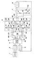
以下、本発明の好適な実施の形態を添付図面を参照して説明する。図1は本発明に係るPLL回路の全体構成を示す回路図であり、PLL回路は、基準信号を発する基準信号源1と、基準信号を分周する分周回路であるRカウンタ2と、後述するVCO8の発振信号を分周する分周回路であるNカウンタ3と、これら両カウンタ2,3の出力信号の位相及び周波数を比較してアップ信号、ダウン信号を出力するとともに、ロック状態を検出してLD信号を出力する位相比較・ロック検出回路4と、この位相比較・ロック検出回路4の出力信号に応じた制御信号を出力する制御回路5と、この制御回路5の制御信号及び前記位相比較・ロック検出回路4の出力信号に応じてホールド状態、チャージ状態、ディスチャージ状態、チャージ・ディスチャージ状態のいずれかとなり、各状態に応じた電流を出力するチャージポンプ回路6と、このチャージポンプ回路6の出力信号の高周波成分を減衰させて低周波成分だけを出力するローパスフィルタ7と、このローパスフィルタ7の出力信号の電圧レベルに応じて前記Rカウンタ2の出力信号の差を縮める方向に動作し、発振信号を出力するVCO8とからなる。
Preferred embodiments of the present invention will be described below with reference to the accompanying drawings. FIG. 1 is a circuit diagram showing the overall configuration of a PLL circuit according to the present invention. The PLL circuit includes a reference signal source 1 that generates a reference signal, an
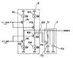
次に、チャージポンプ回路6の構成を図1に基づいてさらに説明する。電源端子と第1PチャネルMOSトランジスタP1(以下トランジスタP1という)のソース端子との間に第1電流源61を接続し、このトランジスタP1のゲート端子は位相比較・ロック検出回路4のアップ信号出力端子41に接続している。接地端子と第1NチャネルMOSトランジスタN1(以下トランジスタN1という)のソース端子との間に第2電流源62を接続し、このトランジスタN1のゲート端子は位相比較・ロック検出回路4のダウン信号出力端子42に接続している。また、前記各トランジスタP1,N1のドレイン端子は、互いに接続して、ローパスフィルタ7を介してVCO8に信号を出力する第1出力端子たるVCO制御端子65に接続している。
Next, the configuration of the
ソース端子をトランジスタP1のソース端子に接続した第2PチャネルMOSトランジスタP2(以下トランジスタP2という)のドレイン端子は、第4電流源64を介して接地端子に接続し、ゲート端子は制御回路5の第1出力端子51に接続している。また、ソース端子をトランジスタN1のソース端子に接続した第2NチャネルMOSトランジスタN2(以下トランジスタN2という)のドレイン端子は、第3電流源63を介して電源端子に接続し、ゲート端子は制御回路5の第4出力端子54に接続している。
The drain terminal of the second P-channel MOS transistor P2 (hereinafter referred to as transistor P2) whose source terminal is connected to the source terminal of the transistor P1 is connected to the ground terminal via the fourth
ソース端子を第3電流源63を介して電源端子に接続した第3PチャネルMOSトランジスタP3(以下トランジスタP3という)のゲート端子は、制御回路5の第2出力端子52に接続している。ソース端子を第4電流源64を介して接地端子に接続した第3NチャネルMOSトランジスタN3(以下トランジスタN3という)のゲート端子は、制御回路5の第3出力端子53に接続している。そして、前記各トランジスタP3,N3のドレイン端子は第2出力端子66に接続し、この第2出力端子66は、ローパスフィルタ7の後述する抵抗71と容量72との間に接続している。
The gate terminal of a third P-channel MOS transistor P3 (hereinafter referred to as transistor P3) whose source terminal is connected to the power supply terminal via the third
なお、図1に示すように、制御回路5は、位相比較・ロック検出回路4の出力信号であるアップ信号、ダウン信号、LD信号がそれぞれ入力する第1入力端子55、第2入力端子56、第3入力端子57の3つの入力端子を有している。前記LD信号は、前記位相比較・ロック検出回路4がロック状態を検出している間出力されるものである。制御回路5の上述した第1出力端子51は、LD信号が出力されている間、アップ信号と逆の信号を出力し、第2出力端子52は、前記LD信号が出力されていない間、アップ信号と同じ信号を出力し、第3出力端子53は、LD信号が出力されていない間、ダウン信号と同じ信号を出力し、第4出力端子54は、LD信号が出力されている間、ダウン信号と逆の信号を出力するよう構成している。
As shown in FIG. 1, the
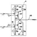
ここで、図2に基づいて上述した各電流源61,62,63,64に定電流を供給する共通の定電流源回路について説明する。電源電池91は、そのプラス側がPチャネルMOSトランジスタP11(以下トランジスタP11という)のゲート端子に接続し、マイナス側が接地端子に接続している。このトランジスタP11のソース端子は電源端子に接続し、そのドレイン端子はNチャネルMOSトランジスタN11(以下トランジスタN11という)のドレイン端子に接続している。前記トランジスタN11のソース端子は接地端子に接続し、そのゲート端子は、前記ドレイン端子に接続するとともに、各NチャネルMOSトランジスタN12,N13,N14(以下それぞれトランジスタN12,N13,N14という)の各ゲート端子に接続している。前記トランジスタN12のソース端子は接地端子に接続し、ドレイン端子は、PチャネルMOSトランジスタP12(以下トランジスタP12という)のドレイン端子とゲート端子に接続している。前記トランジスタP12のソース端子は電源端子に接続し、ゲート端子はさらに各PチャネルMOSトランジスタP13,P14(以下それぞれトランジスタP13,P14という)の各ゲート端子に接続している。前記トランジスタP13のソース端子は電源端子に接続し、ドレイン端子はトランジスタP1,P2の各ドレイン端子に接続している。また、トランジスタP14のソース端子は電源端子に接続し、ドレイン端子はトランジスタP3のソース端子に接続している。一方、前記前記トランジスタN13のソース端子は接地端子に接続し、ドレイン端子はトランジスタN1,N2の各ソース端子に接続している。また、トランジスタN14のソース端子は接地端子に接続し、ドレイン端子はトランジスタN3のソース端子に接続している。
Here, a common constant current source circuit for supplying a constant current to each of the
上述した構成において、トランジスタP11のゲート端子には電源電池91から常に一定の電圧が供給されており、このトランジスタP11がオン動作すると、各トランジスタN11,N12がオン動作するとともに、各トランジスタN13,N14もオン動作する。このとき、前記各トランジスタN11,N12,N13,N14の各ゲート電位は一定なものとなる。また、前記トランジスタN12がオン動作することによって、トランジスタP12がオン動作するとともに、各トランジスタP13,P14もオン動作する。このとき、前記各トランジスタP12,P13,P14の各ゲート電位も一定なものとなる。したがって、各トランジスタP13,P14,N13,N14を介して定電流を供給することができる。すなわち、トランジスタP13を介して電流を供給する構成が電流源61に対応し、トランジスタP14を介して電流を供給する構成が電流源63に対応し、トランジスタN13を介して電流を供給する構成が電流源62に対応し、トランジスタN14を介して電流を供給する構成が電流源64に対応するものである。
In the configuration described above, a constant voltage is always supplied from the
次に、ローパスフィルタ7の構成を図1に基づいて説明する。ローパスフィルタ7はVCO制御端子65に一端を接続した抵抗71の他端を、第1容量72を介して接地端子に接続し、これら抵抗71と第1容量72と並列に、第2容量73をVCO制御端子65と接地端子との間に接続している。また、前記抵抗71と前記第1容量72との間には、第2出力端子66を介して各トランジスタP3,N3の互いに接続したドレイン端子を接続している。例えば、前記抵抗71の抵抗値は29.9kΩ、前記第1容量72の容量値は150.0pF、前記第2容量73の容量値は15.8pFである。本実施形態において、第1容量72の一端は接地端子に接続されているが、これを電源端子に接続することも可能である。
Next, the configuration of the low-pass filter 7 will be described with reference to FIG. The low-pass filter 7 connects the other end of the
続いて、上述したPLL回路の動作を説明する。まず、アンロック状態の場合について説明する。図1においてアンロック状態における制御回路5の出力は、第1出力端子51の電位は常に「H」、第4出力端子54の電位は常に「L」、第2出力端子52の電位はアップ信号と同じ、第3出力端子53の電位はダウン信号と同じとなっている。このため、トランジスタP2とトランジスタN2は常にオフとなっており、この状態でのチャージポンプ回路6とローパスフィルタ7の等価回路図は図3、図4のように表される。
Subsequently, the operation of the above-described PLL circuit will be described. First, the case of the unlocked state will be described. In FIG. 1, the output of the
そして、ホールド状態では、各トランジスタP1,P3,N1,N3は全てオフとなり、VCO制御端子65はハイ・インピーダンスとなる。
In the hold state, all the transistors P1, P3, N1, and N3 are turned off, and the
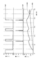
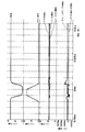
チャージ状態では、図3に示すように、トランジスタP1,P3がオンし、トランジスタP1を介して第2容量73が、また、トランジスタP1と抵抗71を介して第1容量72がIpの電流でチャージされる。また、トランジスタP3を介して第1容量72が抵抗71を介すことなく、Ipの電流でチャージされる。図9に、上述した本実施形態のPLL回路におけるチャージ動作波形を示し、図10に、図13に示す構成の従来例のPLL回路におけるチャージ動作波形を示す。図9と図10とを比較すれば理解できるように、本実施形態においては、ほぼ倍のスピードでVCO制御端子65の電位をチャージできることがわかる。
In the charged state, as shown in FIG. 3, the transistors P1 and P3 are turned on, the
なお、ロックアップタイム(引込み時間)をより速めたい場合は、チャージエラーの抑制効果は低下するが、第1容量72をチャージする各電流源61,63のサイズを大きくすることで可能となる。
If the lock-up time (pull-in time) is to be increased, the effect of suppressing the charge error is reduced, but it is possible by increasing the size of each
ディスチャージ状態では、図4に示すように、トランジスタN1,N3がオンし、トランジスタN1を介して第2容量73が、トランジスタN1と抵抗71を介して第1容量72が、Ipの電流でディスチャージされる。また、トランジスタN3を介して第1容量72が抵抗71を介すことなく、Ipの電流でディスチャージされる。
In the discharge state, as shown in FIG. 4, the transistors N1 and N3 are turned on, the
チャージ・ディスチャージ状態では、すべてのトランジスタP1,P3,N1,N3がオンとなり、チャージ、ディスチャージが同時に行われる。しかし、電流制限されているため、チャージポンプ回路6に2倍のIp以上の電流は流れない。なお、このチャージ・ディスチャージ状態は、位相比較・ロック検出回路4における比較周期毎にごく短時間発生するものである。
In the charge / discharge state, all the transistors P1, P3, N1, and N3 are turned on, and charging and discharging are performed simultaneously. However, since the current is limited, no current more than twice the current Ip flows through the
次にロック状態について説明する。図1においてロック状態での制御回路5の出力は、第2出力端子52の電位は常に「H」、第3出力端子53の電位は常に「L」、第1出力端子51の電位はアップ信号の反転、第4出力端子54の電位はダウン信号の反転となっている。このため、トランジスタP3,N3は常にオフとなっており、この状態のチャージポンプ回路6の等価回路図は図5〜図8のように表される。
Next, the locked state will be described. In FIG. 1, the output of the
ホールド状態では、図5に示すように、各トランジスタP2,N2はオンとなり、各トランジスタP1,N1はオフとなっている。このとき、VCO制御端子65はハイ・インピーダンスとなっているが、前記各トランジスタP2,N2を介して一定の電流がチャージポンプ回路6には流れており、また、前記各トランジスタP2,N2のソース端子側67,68の電位は上下の各電流源61,64,63,62よって決定される中間的な電位となっており、かつ、第1電流源61と第3電流源63、第2電流源62と第4電流源64のサイズがそれぞれ等しいならば、前記各トランジスタP2,N2のソース端子側67,68の電位はほぼ等しくなっている。
In the hold state, as shown in FIG. 5, the transistors P2 and N2 are turned on, and the transistors P1 and N1 are turned off. At this time, although the
ホールド状態からチャージ・ディスチャージ状態に遷移した場合、図6に示すように、各トランジスタP1,N1がオンし、各トランジスタP2,N2がオフとなる。ロック状態では、VCO制御端子65の電位はほぼ中間電位であるため、少ない電位差でVCO制御端子65と各トランジスタP1,N1のソース端子側67,68は接続され、各電流源61,62の寄生容量の電荷共有によるチャージエラーを低減することができる。なお、前記各トランジスタP1,N1のソース端子側67,68の電位はほぼ等しくなっているため、これらの間では電荷共有は発生しない。
When transitioning from the hold state to the charge / discharge state, as shown in FIG. 6, the transistors P1 and N1 are turned on, and the transistors P2 and N2 are turned off. In the locked state, since the potential of the
また、ホールド状態およびチャージ・ディスチャージ状態のいずれにおいても、チャージポンプ回路6には常に電流が流れているため、状態変化により電源に与えるノイズの影響も少ない。
In both the hold state and the charge / discharge state, a current always flows through the
チャージ状態では、図7に示すように、各トランジスタP1,N2がオンし、各トランジスタP2,N1がオフとなり、VCO制御端子65がトランジスタP1を介したIpの電流でチャージされる。この場合も、VCO制御端子65とトランジスタP1のソース端子側67は少ない電位差で接続される。また、このチャージ状態においてもチャージポンプ回路6には常に電流が流れている。
In the charged state, as shown in FIG. 7, the transistors P1 and N2 are turned on, the transistors P2 and N1 are turned off, and the
ディスチャージ状態では、図8に示すように、各トランジスタP2,N1がオンし、各トランジスタP1,N2がオフとなり、VCO制御端子65がトランジスタN1を介してIpの電流でディスチャージされる。この場合も、VCO制御端子65とトランジスタN1のソース端子側68は少ない電位差で接続される。また、このディスチャージ状態においてもチャージポンプ回路6には常に電流が流れている。
In the discharge state, as shown in FIG. 8, the transistors P2 and N1 are turned on, the transistors P1 and N2 are turned off, and the
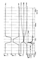
図11に、本実施形態におけるPLL回路のロック時のチャージ・ディスチャージ動作波形を示し、図12に、図13に示す従来例におけるPLL回路のロック時のチャージ・ディスチャージ動作波形を示す。両図から理解できるように、本発実施形態においては、従来例と比較してチャージポンプ回路に発生するノイズと、チャージエラーを、1/3以上低減できることがわかる。 FIG. 11 shows charge / discharge operation waveforms when the PLL circuit in the present embodiment is locked, and FIG. 12 shows charge / discharge operation waveforms when the PLL circuit in the conventional example shown in FIG. 13 is locked. As can be understood from both figures, in the present embodiment, it is understood that noise generated in the charge pump circuit and charge error can be reduced by 1/3 or more as compared with the conventional example.
1 基準信号源
2 Rカウンタ
3 Nカウンタ
4 位相比較・ロック検出回路
5 制御回路
6 チャージポンプ回路
7 ローパスフィルタ
8 VCO
61,62,63,64 電流源
65 VCO制御端子
66 第2出力端子
71 抵抗
72,73 容量
P1,P2,P3 PチャネルMOSトランジスタ
N1,N2,N3 NチャネルMOSトランジスタ
1 Reference signal source 2 R counter 3
61, 62, 63, 64
Claims (3)
電源端子と第1PチャネルMOSトランジスタのソース端子との間に第1電流源を接続し、接地端子と第1NチャネルMOSトランジスタのソース端子との間に第2電流源を接続し、電源端子と第3PチャネルMOSトランジスタのソース端子との間に第3電流源を接続し、接地端子と第3NチャネルMOSトランジスタのソース端子との間に第4電流源を接続し、前記第1PチャネルMOSトランジスタと前記第1NチャネルMOSトランジスタの各ドレイン端子を、前記第1出力端子に接続し、前記第3PチャネルMOSトランジスタと前記第3NチャネルMOSトランジスタの各ドレイン端子を、前記ローパスフィルタの抵抗と第1容量との間に接続した第2出力端子に接続し、前記第1PチャネルMOSトランジスタと前記第3PチャネルMOSトランジスタの各ゲート端子には、前記第1容量および第2容量をチャージするための同一のアップ信号が入力し、前記第1NチャネルMOSトランジスタと前記第3NチャネルMOSトランジスタの各ゲート端子には、前記第1容量および第2容量をディスチャージするための同一のダウン信号が入力するよう構成した
ことを特徴とするチャージポンプ回路。 A resistor and a first capacitor connected in series from the first output terminal side in series between the first output terminal and the ground, and a resistor and a first capacitor connected in parallel to the first output terminal and the ground. A charge pump circuit that outputs to the low-pass filter having the second capacitance via the first output terminal,
A first current source connected between a power supply terminal and the source terminal of the 1P-channel MOS transistor, a second current source connected between the ground terminal and the source terminal of the 1N-channel MOS transistor, a power supply terminal and the A third current source is connected between the source terminal of the 3P channel MOS transistor , a fourth current source is connected between the ground terminal and the source terminal of the third N channel MOS transistor, and the first P channel MOS transistor and the Each drain terminal of the first N-channel MOS transistor is connected to the first output terminal, and each drain terminal of the third P-channel MOS transistor and the third N-channel MOS transistor is connected to a resistor and a first capacitor of the low-pass filter. A second output terminal connected between the first P-channel MOS transistor and the third P-channel; The same up signal for charging the first capacitor and the second capacitor is input to each gate terminal of the n-channel MOS transistor, and each gate terminal of the first N-channel MOS transistor and the third N-channel MOS transistor is connected to each gate terminal. The charge pump circuit is configured to receive the same down signal for discharging the first capacitor and the second capacitor .
前記チャージポンプ回路は、電源端子と第1PチャネルMOSトランジスタのソース端子との間に第1電流源を接続し、接地端子と第1NチャネルMOSトランジスタのソース端子との間に第2電流源を接続し、電源端子と第2NチャネルMOSトランジスタのドレイン端子との間に第3電流源を接続し、接地端子と第2PチャネルMOSトランジスタのドレイン端子との間に第4電流源を接続し、前記第3電流源と前記第2NチャネルMOSトランジスタのドレイン端子とに第3PチャネルMOSトランジスタのソース端子を接続し、前記第4電流源と前記第2PチャネルMOSトランジスタのドレイン端子とに第3NチャネルMOSトランジスタのソース端子を接続し、前記第3PチャネルMOSトランジスタと前記第3NチャネルMOSトランジスタの各ドレイン端子を第2出力端子に接続し、前記第1PチャネルMOSトランジスタと前記第1NチャネルMOSトランジスタの各ドレイン端子を第1出力端子に接続し、前記第1PチャネルMOSトランジスタと前記第2PチャネルMOSトランジスタのソース端子同士を接続し、前記第1NチャネルMOSトランジスタと前記第2NチャネルMOSトランジスタのソース端子同士を接続し、前記第1Pチャネルトランジスタのゲート端子は前記位相比較・ロック検出回路のアップ信号出力端子に接続し、前記第1Nチャネルトランジスタのゲート端子は前記位相比較・ロック検出回路のダウン信号出力端子に接続して構成し、前記制御回路は、前記位相比較・ロック検出回路のアップ信号が入力する第1入力端子と、前記位相比較・ロック検出回路のダウン信号が入力する第2入力端子と、前記位相比較・ロック検出回路のロック検出信号が入力する第3入力端子とを有する一方、ロック検出信号が入力している間アップ信号を反転した信号を出力する第1出力端子と、ロック検出信号が入力していない間アップ信号と同じ信号を出力する第2出力端子と、ロック検出信号が入力していない間ダウン信号と同じ信号を出力する第3出力端子と、ロック検出信号が入力している間ダウン信号を反転した信号を出力する第4出力端子を有し、前記第1出力端子は前記第2PチャネルMOSトランジスタのゲート端子に接続し、前記第2出力端子は前記第3PチャネルMOSトランジスタのゲート端子に接続し、前記第3出力端子は前記第3NチャネルMOSトランジスタのゲート端子に接続し、前記第4出力端子は前記第2NチャネルMOSトランジスタのゲート端子に接続した
ことを特徴とするチャージポンプ回路。 A charge pump circuit that receives a control signal of a control circuit that generates a control signal according to an output of a phase comparison / lock detection circuit ,
The charge pump circuit connects a first current source between a power supply terminal and the source terminal of the first P-channel MOS transistor, and connects a second current source between the ground terminal and the source terminal of the first N-channel MOS transistor. A third current source is connected between the power supply terminal and the drain terminal of the second N-channel MOS transistor; a fourth current source is connected between the ground terminal and the drain terminal of the second P-channel MOS transistor; the third current source and the drain terminal of the first 2N-channel MOS transistor source terminal of the 3 P-channel MOS transistor and connected, the 3N-channel MOS to the drain terminal of said first 2P channel MOS transistor and the fourth current source A source terminal of the transistor is connected, and the third P-channel MOS transistor and the third N-channel MO are connected. Each drain terminal of the S transistor is connected to a second output terminal, each drain terminal of the first P-channel MOS transistor and the first N-channel MOS transistor is connected to a first output terminal, and the first P-channel MOS transistor and the first The source terminals of the 2P channel MOS transistors are connected to each other, the source terminals of the first N channel MOS transistor and the second N channel MOS transistor are connected to each other, and the gate terminal of the first P channel transistor is connected to the phase comparison / lock detection circuit. The first N-channel transistor is connected to the up signal output terminal, the gate terminal of the first N-channel transistor is connected to the down signal output terminal of the phase comparison / lock detection circuit, and the control circuit is connected to the phase comparison / lock detection circuit. A first input terminal for inputting a signal; While having a second input terminal for inputting a down signal of the phase comparison / lock detection circuit and a third input terminal for inputting a lock detection signal of the phase comparison / lock detection circuit, while the lock detection signal is being input A first output terminal that outputs a signal obtained by inverting the up signal, a second output terminal that outputs the same signal as the up signal while the lock detection signal is not input, and a down signal while the lock detection signal is not input A third output terminal that outputs the same signal; and a fourth output terminal that outputs a signal obtained by inverting the down signal while the lock detection signal is being input. The first output terminal is connected to the second P-channel MOS transistor. The second output terminal is connected to the gate terminal of the third P-channel MOS transistor, and the third output terminal is connected to the third N-channel MOS transistor. The charge pump circuit is connected to the gate terminal of data, the fourth output terminal, characterized in that connected to the gate terminal of the first 2N-channel MOS transistor.
ことを特徴とするPLL回路。 A voltage-controlled oscillation circuit that outputs an oscillation signal corresponding to the voltage level of the input signal, a reference signal source that issues a reference signal, an R counter that is a frequency-dividing circuit that divides the reference signal, and oscillation of the voltage-controlled oscillation circuit The N counter, which is a frequency dividing circuit that divides the signal, compares the phase and frequency of the output signals of both counters, outputs an up signal and a down signal, and detects a lock state and outputs a lock detection signal. A phase comparison / lock detection circuit, a control circuit for outputting a control signal corresponding to the output signal of the phase comparison / lock detection circuit, and a current corresponding to the output signal of the control circuit and the phase comparison / lock detection circuit are output. The charge pump circuit according to claim 1 or 2, and a high frequency component of an output signal of the charge pump circuit is attenuated to control only the low frequency component. PLL circuit, comprising the low-pass filter for outputting the oscillation circuit.
Priority Applications (2)
| Application Number | Priority Date | Filing Date | Title |
|---|---|---|---|
| JP2004132017A JP4371893B2 (en) | 2004-04-27 | 2004-04-27 | Charge pump circuit and PLL circuit using the charge pump circuit |
| US11/109,299 US7271619B2 (en) | 2004-04-27 | 2005-04-18 | Charge pump circuit reducing noise and charge error and PLL circuit using the same |
Applications Claiming Priority (1)
| Application Number | Priority Date | Filing Date | Title |
|---|---|---|---|
| JP2004132017A JP4371893B2 (en) | 2004-04-27 | 2004-04-27 | Charge pump circuit and PLL circuit using the charge pump circuit |
Publications (3)
| Publication Number | Publication Date |
|---|---|
| JP2005318122A JP2005318122A (en) | 2005-11-10 |
| JP2005318122A5 JP2005318122A5 (en) | 2007-06-14 |
| JP4371893B2 true JP4371893B2 (en) | 2009-11-25 |
Family
ID=35135801
Family Applications (1)
| Application Number | Title | Priority Date | Filing Date |
|---|---|---|---|
| JP2004132017A Expired - Fee Related JP4371893B2 (en) | 2004-04-27 | 2004-04-27 | Charge pump circuit and PLL circuit using the charge pump circuit |
Country Status (2)
| Country | Link |
|---|---|
| US (1) | US7271619B2 (en) |
| JP (1) | JP4371893B2 (en) |
Families Citing this family (14)
| Publication number | Priority date | Publication date | Assignee | Title |
|---|---|---|---|---|
| KR100723511B1 (en) | 2005-11-14 | 2007-05-30 | 삼성전자주식회사 | Charge pump circuit, and phase locked loop circuit and delay locked loop circuit including the circuit |
| US7501867B2 (en) * | 2006-09-14 | 2009-03-10 | Rambus, Inc. | Power supply noise rejection in PLL or DLL circuits |
| US7915933B2 (en) * | 2006-11-30 | 2011-03-29 | Mosaid Technologies Incorporated | Circuit for clamping current in a charge pump |
| JP2009200703A (en) * | 2008-02-20 | 2009-09-03 | Toshiba Corp | Charge pump circuit, and pll circuit |
| US8674753B2 (en) * | 2008-06-03 | 2014-03-18 | Texas Instruments Incorporated | Systems and methods for cancelling phase-locked loop supply noise |
| US7768326B2 (en) * | 2008-09-18 | 2010-08-03 | Kabushiki Kaisha Toshiba | Wide range operational charge pump circuit |
| US8183913B2 (en) * | 2010-02-17 | 2012-05-22 | Taiwan Semiconductor Manufacturing Company, Ltd. | Integrated circuits including a charge pump circuit and operating methods thereof |
| US8525564B2 (en) * | 2010-10-20 | 2013-09-03 | University Of Southern California | Charge-based phase locked loop charge pump |
| CN102957316A (en) * | 2011-08-31 | 2013-03-06 | 深圳艾科创新微电子有限公司 | Low-charge-injection charge pump and low charge injection method |
| TWI499215B (en) * | 2012-10-17 | 2015-09-01 | Mstar Semiconductor Inc | Charging/discharging circuit and pll utilizing the charging/discharging circuit |
| CN106059573B (en) * | 2016-05-30 | 2019-03-29 | 中国电子科技集团公司第二十四研究所 | Reduce the circuit and method of the charge pump phase locking loop circuit switching signal amplitude of oscillation |
| US10103140B2 (en) * | 2016-10-14 | 2018-10-16 | Alpha And Omega Semiconductor Incorporated | Switch circuit with controllable phase node ringing |
| CN106961273B (en) * | 2017-04-12 | 2020-05-26 | 西安电子科技大学 | Charge pump circuit based on stable anti-creeping protection and current sink control technology |
| CN113437967B (en) * | 2021-07-02 | 2023-07-07 | 电子科技大学 | Low-noise millimeter wave phase-locked loop frequency synthesizer based on time error amplifier |
Family Cites Families (13)
| Publication number | Priority date | Publication date | Assignee | Title |
|---|---|---|---|---|
| JP3196409B2 (en) * | 1993-03-22 | 2001-08-06 | 住友金属工業株式会社 | PLL circuit |
| JP3338748B2 (en) * | 1996-01-30 | 2002-10-28 | 日本電気株式会社 | PLL frequency synthesizer |
| JP2877196B2 (en) * | 1996-03-28 | 1999-03-31 | 日本電気株式会社 | Charge pump circuit and phase locked loop circuit having the same |
| JPH09307436A (en) * | 1996-05-10 | 1997-11-28 | Nippon Motorola Ltd | Pll circuit |
| EP0841753A3 (en) * | 1996-11-07 | 1999-12-15 | Nortel Networks Corporation | Charge pump circuit |
| JP4069503B2 (en) | 1998-07-17 | 2008-04-02 | ソニー株式会社 | PLL circuit |
| US6222402B1 (en) * | 1998-09-04 | 2001-04-24 | International Business Machines Corporation | Differential charge-pump with improved linearity |
| JP2000165235A (en) * | 1998-11-30 | 2000-06-16 | Sharp Corp | Charge pump circuit and pll frequency synthesizer circuit using it |
| JP3583646B2 (en) * | 1999-03-30 | 2004-11-04 | 株式会社ルネサステクノロジ | Phase locked loop |
| JP2001274682A (en) * | 2000-03-27 | 2001-10-05 | Toshiba Corp | Phase locked loop circuit |
| JP2002330067A (en) * | 2001-05-01 | 2002-11-15 | Sony Corp | Charge pump circuit and phase synchronizing loop circuit |
| JP3748414B2 (en) * | 2002-02-07 | 2006-02-22 | 日本電信電話株式会社 | Phase-locked loop circuit |
| US6710666B1 (en) * | 2002-11-07 | 2004-03-23 | Mediatek Inc. | Charge pump structure for reducing capacitance in loop filter of a phase locked loop |
-
2004
- 2004-04-27 JP JP2004132017A patent/JP4371893B2/en not_active Expired - Fee Related
-
2005
- 2005-04-18 US US11/109,299 patent/US7271619B2/en active Active
Also Published As
| Publication number | Publication date |
|---|---|
| US7271619B2 (en) | 2007-09-18 |
| US20050237092A1 (en) | 2005-10-27 |
| JP2005318122A (en) | 2005-11-10 |
Similar Documents
| Publication | Publication Date | Title |
|---|---|---|
| US7271619B2 (en) | Charge pump circuit reducing noise and charge error and PLL circuit using the same | |
| US8810292B2 (en) | PLL circuit | |
| US8306175B2 (en) | Clock and data recovery circuit | |
| US7161401B2 (en) | Wide output-range charge pump with active biasing current | |
| JP2007097140A (en) | Delay cell of voltage controlled delay line using digital and analog control scheme | |
| US8358729B2 (en) | Baseband phase-locked loop | |
| JPWO2008146433A1 (en) | Spread spectrum control PLL circuit and startup method thereof | |
| JPH0964727A (en) | Synchronization circuit | |
| JP4482524B2 (en) | PLL circuit with leakage current compensation circuit | |
| US8542073B2 (en) | Variable-capacitance device | |
| US20120170699A1 (en) | Method to decrease locktime in a phase locked loop | |
| US6624706B2 (en) | Automatic bias adjustment circuit for use in PLL circuit | |
| JPH11225069A (en) | Charge pump circuit, pll circuit and pll frequency synthesizer | |
| US8575979B2 (en) | Fully differential adaptive bandwidth PLL with differential supply regulation | |
| US20070063687A1 (en) | Circuit and method for bias voltage generation | |
| Lee et al. | A 5-Gb/s digital clock and data recovery circuit with reduced DCO supply noise sensitivity utilizing coupling network | |
| JP4636107B2 (en) | PLL circuit | |
| US10361706B2 (en) | Clock and data recovery (CDR) circuit | |
| JP2007295180A (en) | Charge pump circuit, and pll circuit and dll circuit using same | |
| WO2018177195A1 (en) | Charge pump, charge pump-based processing method and phase-locked loop circuit, and storage medium | |
| JP4510039B2 (en) | Phase synchronization circuit | |
| JPWO2005008895A1 (en) | Charge pump circuit | |
| JP4635914B2 (en) | PLL circuit | |
| JP2003298414A (en) | Semiconductor integrated circuit | |
| JP2013247619A (en) | Current control circuit and pll circuit using the same |
Legal Events
| Date | Code | Title | Description |
|---|---|---|---|
| A521 | Request for written amendment filed |
Free format text: JAPANESE INTERMEDIATE CODE: A523 Effective date: 20070423 |
|
| A621 | Written request for application examination |
Free format text: JAPANESE INTERMEDIATE CODE: A621 Effective date: 20070423 |
|
| RD02 | Notification of acceptance of power of attorney |
Free format text: JAPANESE INTERMEDIATE CODE: A7422 Effective date: 20080409 |
|
| RD04 | Notification of resignation of power of attorney |
Free format text: JAPANESE INTERMEDIATE CODE: A7424 Effective date: 20080418 |
|
| A977 | Report on retrieval |
Free format text: JAPANESE INTERMEDIATE CODE: A971007 Effective date: 20090213 |
|
| A131 | Notification of reasons for refusal |
Free format text: JAPANESE INTERMEDIATE CODE: A131 Effective date: 20090310 |
|
| A521 | Request for written amendment filed |
Free format text: JAPANESE INTERMEDIATE CODE: A523 Effective date: 20090508 |
|
| TRDD | Decision of grant or rejection written | ||
| A01 | Written decision to grant a patent or to grant a registration (utility model) |
Free format text: JAPANESE INTERMEDIATE CODE: A01 Effective date: 20090811 |
|
| A01 | Written decision to grant a patent or to grant a registration (utility model) |
Free format text: JAPANESE INTERMEDIATE CODE: A01 |
|
| A61 | First payment of annual fees (during grant procedure) |
Free format text: JAPANESE INTERMEDIATE CODE: A61 Effective date: 20090901 |
|
| FPAY | Renewal fee payment (event date is renewal date of database) |
Free format text: PAYMENT UNTIL: 20120911 Year of fee payment: 3 |
|
| R150 | Certificate of patent or registration of utility model |
Ref document number: 4371893 Country of ref document: JP Free format text: JAPANESE INTERMEDIATE CODE: R150 Free format text: JAPANESE INTERMEDIATE CODE: R150 |
|
| FPAY | Renewal fee payment (event date is renewal date of database) |
Free format text: PAYMENT UNTIL: 20130911 Year of fee payment: 4 |
|
| R250 | Receipt of annual fees |
Free format text: JAPANESE INTERMEDIATE CODE: R250 |
|
| R250 | Receipt of annual fees |
Free format text: JAPANESE INTERMEDIATE CODE: R250 |
|
| R250 | Receipt of annual fees |
Free format text: JAPANESE INTERMEDIATE CODE: R250 |
|
| R250 | Receipt of annual fees |
Free format text: JAPANESE INTERMEDIATE CODE: R250 |
|
| R250 | Receipt of annual fees |
Free format text: JAPANESE INTERMEDIATE CODE: R250 |
|
| R250 | Receipt of annual fees |
Free format text: JAPANESE INTERMEDIATE CODE: R250 |
|
| LAPS | Cancellation because of no payment of annual fees |