JP4362760B2 - Semiconductor single crystal manufacturing equipment - Google Patents
Semiconductor single crystal manufacturing equipment Download PDFInfo
- Publication number
- JP4362760B2 JP4362760B2 JP2003353962A JP2003353962A JP4362760B2 JP 4362760 B2 JP4362760 B2 JP 4362760B2 JP 2003353962 A JP2003353962 A JP 2003353962A JP 2003353962 A JP2003353962 A JP 2003353962A JP 4362760 B2 JP4362760 B2 JP 4362760B2
- Authority
- JP
- Japan
- Prior art keywords
- wire
- manufacturing apparatus
- single crystal
- chamber
- seed holder
- Prior art date
- Legal status (The legal status is an assumption and is not a legal conclusion. Google has not performed a legal analysis and makes no representation as to the accuracy of the status listed.)
- Expired - Lifetime
Links
- 239000004065 semiconductor Substances 0.000 title claims description 64
- 238000004519 manufacturing process Methods 0.000 title claims description 55
- 239000013078 crystal Substances 0.000 title claims description 54
- 239000000155 melt Substances 0.000 claims description 10
- 238000004804 winding Methods 0.000 claims description 6
- 238000010438 heat treatment Methods 0.000 claims description 3
- 239000007788 liquid Substances 0.000 description 21
- XUIMIQQOPSSXEZ-UHFFFAOYSA-N Silicon Chemical compound [Si] XUIMIQQOPSSXEZ-UHFFFAOYSA-N 0.000 description 16
- 229910052710 silicon Inorganic materials 0.000 description 16
- 239000010703 silicon Substances 0.000 description 16
- 230000006866 deterioration Effects 0.000 description 12
- 238000006243 chemical reaction Methods 0.000 description 10
- 239000002994 raw material Substances 0.000 description 10
- WFKWXMTUELFFGS-UHFFFAOYSA-N tungsten Chemical compound [W] WFKWXMTUELFFGS-UHFFFAOYSA-N 0.000 description 9
- 238000000034 method Methods 0.000 description 8
- 229910052721 tungsten Inorganic materials 0.000 description 7
- 239000010937 tungsten Substances 0.000 description 7
- 230000003647 oxidation Effects 0.000 description 6
- 238000007254 oxidation reaction Methods 0.000 description 6
- 239000000463 material Substances 0.000 description 5
- 238000010586 diagram Methods 0.000 description 4
- 239000007789 gas Substances 0.000 description 4
- 239000011810 insulating material Substances 0.000 description 4
- 150000001875 compounds Chemical class 0.000 description 3
- 238000003780 insertion Methods 0.000 description 3
- 230000037431 insertion Effects 0.000 description 3
- 229910021421 monocrystalline silicon Inorganic materials 0.000 description 3
- 239000010453 quartz Substances 0.000 description 3
- VYPSYNLAJGMNEJ-UHFFFAOYSA-N silicon dioxide Inorganic materials O=[Si]=O VYPSYNLAJGMNEJ-UHFFFAOYSA-N 0.000 description 3
- JBRZTFJDHDCESZ-UHFFFAOYSA-N AsGa Chemical compound [As]#[Ga] JBRZTFJDHDCESZ-UHFFFAOYSA-N 0.000 description 2
- 229910001218 Gallium arsenide Inorganic materials 0.000 description 2
- 230000005540 biological transmission Effects 0.000 description 2
- 239000000470 constituent Substances 0.000 description 2
- 239000011162 core material Substances 0.000 description 2
- 238000007789 sealing Methods 0.000 description 2
- OKTJSMMVPCPJKN-UHFFFAOYSA-N Carbon Chemical compound [C] OKTJSMMVPCPJKN-UHFFFAOYSA-N 0.000 description 1
- ZOKXTWBITQBERF-UHFFFAOYSA-N Molybdenum Chemical compound [Mo] ZOKXTWBITQBERF-UHFFFAOYSA-N 0.000 description 1
- 230000032683 aging Effects 0.000 description 1
- QVGXLLKOCUKJST-UHFFFAOYSA-N atomic oxygen Chemical compound [O] QVGXLLKOCUKJST-UHFFFAOYSA-N 0.000 description 1
- 229910052799 carbon Inorganic materials 0.000 description 1
- 230000015556 catabolic process Effects 0.000 description 1
- 238000006731 degradation reaction Methods 0.000 description 1
- 230000008021 deposition Effects 0.000 description 1
- 239000011261 inert gas Substances 0.000 description 1
- 238000007689 inspection Methods 0.000 description 1
- 229910052750 molybdenum Inorganic materials 0.000 description 1
- 239000011733 molybdenum Substances 0.000 description 1
- QGLKJKCYBOYXKC-UHFFFAOYSA-N nonaoxidotritungsten Chemical compound O=[W]1(=O)O[W](=O)(=O)O[W](=O)(=O)O1 QGLKJKCYBOYXKC-UHFFFAOYSA-N 0.000 description 1
- 230000001590 oxidative effect Effects 0.000 description 1
- 229910052760 oxygen Inorganic materials 0.000 description 1
- 239000001301 oxygen Substances 0.000 description 1
- 230000000737 periodic effect Effects 0.000 description 1
- 230000000630 rising effect Effects 0.000 description 1
- 229910001220 stainless steel Inorganic materials 0.000 description 1
- 239000010935 stainless steel Substances 0.000 description 1
- 239000000758 substrate Substances 0.000 description 1
- 229910001930 tungsten oxide Inorganic materials 0.000 description 1
Images


Classifications
-
- C—CHEMISTRY; METALLURGY
- C30—CRYSTAL GROWTH
- C30B—SINGLE-CRYSTAL GROWTH; UNIDIRECTIONAL SOLIDIFICATION OF EUTECTIC MATERIAL OR UNIDIRECTIONAL DEMIXING OF EUTECTOID MATERIAL; REFINING BY ZONE-MELTING OF MATERIAL; PRODUCTION OF A HOMOGENEOUS POLYCRYSTALLINE MATERIAL WITH DEFINED STRUCTURE; SINGLE CRYSTALS OR HOMOGENEOUS POLYCRYSTALLINE MATERIAL WITH DEFINED STRUCTURE; AFTER-TREATMENT OF SINGLE CRYSTALS OR A HOMOGENEOUS POLYCRYSTALLINE MATERIAL WITH DEFINED STRUCTURE; APPARATUS THEREFOR
- C30B29/00—Single crystals or homogeneous polycrystalline material with defined structure characterised by the material or by their shape
- C30B29/02—Elements
- C30B29/06—Silicon
-
- C—CHEMISTRY; METALLURGY
- C30—CRYSTAL GROWTH
- C30B—SINGLE-CRYSTAL GROWTH; UNIDIRECTIONAL SOLIDIFICATION OF EUTECTIC MATERIAL OR UNIDIRECTIONAL DEMIXING OF EUTECTOID MATERIAL; REFINING BY ZONE-MELTING OF MATERIAL; PRODUCTION OF A HOMOGENEOUS POLYCRYSTALLINE MATERIAL WITH DEFINED STRUCTURE; SINGLE CRYSTALS OR HOMOGENEOUS POLYCRYSTALLINE MATERIAL WITH DEFINED STRUCTURE; AFTER-TREATMENT OF SINGLE CRYSTALS OR A HOMOGENEOUS POLYCRYSTALLINE MATERIAL WITH DEFINED STRUCTURE; APPARATUS THEREFOR
- C30B15/00—Single-crystal growth by pulling from a melt, e.g. Czochralski method
- C30B15/32—Seed holders, e.g. chucks
-
- Y—GENERAL TAGGING OF NEW TECHNOLOGICAL DEVELOPMENTS; GENERAL TAGGING OF CROSS-SECTIONAL TECHNOLOGIES SPANNING OVER SEVERAL SECTIONS OF THE IPC; TECHNICAL SUBJECTS COVERED BY FORMER USPC CROSS-REFERENCE ART COLLECTIONS [XRACs] AND DIGESTS
- Y10—TECHNICAL SUBJECTS COVERED BY FORMER USPC
- Y10S—TECHNICAL SUBJECTS COVERED BY FORMER USPC CROSS-REFERENCE ART COLLECTIONS [XRACs] AND DIGESTS
- Y10S117/00—Single-crystal, oriented-crystal, and epitaxy growth processes; non-coating apparatus therefor
- Y10S117/911—Seed or rod holders
-
- Y—GENERAL TAGGING OF NEW TECHNOLOGICAL DEVELOPMENTS; GENERAL TAGGING OF CROSS-SECTIONAL TECHNOLOGIES SPANNING OVER SEVERAL SECTIONS OF THE IPC; TECHNICAL SUBJECTS COVERED BY FORMER USPC CROSS-REFERENCE ART COLLECTIONS [XRACs] AND DIGESTS
- Y10—TECHNICAL SUBJECTS COVERED BY FORMER USPC
- Y10T—TECHNICAL SUBJECTS COVERED BY FORMER US CLASSIFICATION
- Y10T117/00—Single-crystal, oriented-crystal, and epitaxy growth processes; non-coating apparatus therefor
- Y10T117/10—Apparatus
- Y10T117/1024—Apparatus for crystallization from liquid or supercritical state
- Y10T117/1032—Seed pulling
- Y10T117/1052—Seed pulling including a sectioned crucible [e.g., double crucible, baffle]
-
- Y—GENERAL TAGGING OF NEW TECHNOLOGICAL DEVELOPMENTS; GENERAL TAGGING OF CROSS-SECTIONAL TECHNOLOGIES SPANNING OVER SEVERAL SECTIONS OF THE IPC; TECHNICAL SUBJECTS COVERED BY FORMER USPC CROSS-REFERENCE ART COLLECTIONS [XRACs] AND DIGESTS
- Y10—TECHNICAL SUBJECTS COVERED BY FORMER USPC
- Y10T—TECHNICAL SUBJECTS COVERED BY FORMER US CLASSIFICATION
- Y10T117/00—Single-crystal, oriented-crystal, and epitaxy growth processes; non-coating apparatus therefor
- Y10T117/10—Apparatus
- Y10T117/1024—Apparatus for crystallization from liquid or supercritical state
- Y10T117/1032—Seed pulling
- Y10T117/1068—Seed pulling including heating or cooling details [e.g., shield configuration]
-
- Y—GENERAL TAGGING OF NEW TECHNOLOGICAL DEVELOPMENTS; GENERAL TAGGING OF CROSS-SECTIONAL TECHNOLOGIES SPANNING OVER SEVERAL SECTIONS OF THE IPC; TECHNICAL SUBJECTS COVERED BY FORMER USPC CROSS-REFERENCE ART COLLECTIONS [XRACs] AND DIGESTS
- Y10—TECHNICAL SUBJECTS COVERED BY FORMER USPC
- Y10T—TECHNICAL SUBJECTS COVERED BY FORMER US CLASSIFICATION
- Y10T117/00—Single-crystal, oriented-crystal, and epitaxy growth processes; non-coating apparatus therefor
- Y10T117/10—Apparatus
- Y10T117/1024—Apparatus for crystallization from liquid or supercritical state
- Y10T117/1032—Seed pulling
- Y10T117/1072—Seed pulling including details of means providing product movement [e.g., shaft guides, servo means]
-
- Y—GENERAL TAGGING OF NEW TECHNOLOGICAL DEVELOPMENTS; GENERAL TAGGING OF CROSS-SECTIONAL TECHNOLOGIES SPANNING OVER SEVERAL SECTIONS OF THE IPC; TECHNICAL SUBJECTS COVERED BY FORMER USPC CROSS-REFERENCE ART COLLECTIONS [XRACs] AND DIGESTS
- Y10—TECHNICAL SUBJECTS COVERED BY FORMER USPC
- Y10T—TECHNICAL SUBJECTS COVERED BY FORMER US CLASSIFICATION
- Y10T117/00—Single-crystal, oriented-crystal, and epitaxy growth processes; non-coating apparatus therefor
- Y10T117/10—Apparatus
- Y10T117/1024—Apparatus for crystallization from liquid or supercritical state
- Y10T117/1076—Apparatus for crystallization from liquid or supercritical state having means for producing a moving solid-liquid-solid zone
- Y10T117/1088—Apparatus for crystallization from liquid or supercritical state having means for producing a moving solid-liquid-solid zone including heating or cooling details
Description
本発明は、半導体インゴット(例えば、単結晶シリコンのような半導体単結晶や、ガリウム砒素などの化合物半導体)を成長させる半導体単結晶製造装置に関するものである。 The present invention relates to a semiconductor single crystal manufacturing apparatus for growing a semiconductor ingot (for example, a semiconductor single crystal such as single crystal silicon or a compound semiconductor such as gallium arsenide).
従来から、半導体素子の基板には、主として高純度の単結晶シリコンのような半導体単結晶やガリウム砒素などの化合物半導体が用いられているが、この半導体の製造方法の一つとして、ルツボ内の原料融液から円柱状のインゴットを引き上げるCZ法(チョクラルスキー法)が知られている。 Conventionally, a semiconductor single crystal such as high-purity single crystal silicon or a compound semiconductor such as gallium arsenide has been used for a substrate of a semiconductor element. As one method of manufacturing this semiconductor, A CZ method (Czochralski method) for pulling up a cylindrical ingot from a raw material melt is known.
このCZ法は、まず、半導体インゴット製造装置のチャンバ内に設置したルツボに原料である素材を充填し、そのルツボの周囲に設けたヒータによって原料を加熱溶解させる。そして、シードホルダに取り付けた種結晶を融液に着液させ、シードホルダ及びルツボを互いに同方向または逆方向に回転しつつシードホルダを引き上げて、所定の大きさの円柱状のインゴットを成長させる。その後、このインゴットを薄くスライスすることで半導体集積回路等に使用するシリコンウェーハを製作する(例えば、特許文献1参照)。 In the CZ method, first, a raw material is filled in a crucible installed in a chamber of a semiconductor ingot manufacturing apparatus, and the raw material is heated and melted by a heater provided around the crucible. Then, the seed crystal attached to the seed holder is deposited in the melt, and the seed holder is pulled up while rotating the seed holder and the crucible in the same direction or in the opposite direction to grow a cylindrical ingot of a predetermined size. . Then, a silicon wafer used for a semiconductor integrated circuit or the like is manufactured by thinly slicing the ingot (see, for example, Patent Document 1).
図6は、このようなCZ法による半導体インゴット製造装置を示している。図6(A)はシードホルダに取り付けた種結晶を融液に着液している状態の説明図、図6(B)はシードホルダを引き上げてインゴットを成長させた状態の説明図である。 FIG. 6 shows a semiconductor ingot manufacturing apparatus using such a CZ method. FIG. 6A is an explanatory diagram of a state in which the seed crystal attached to the seed holder is deposited in the melt, and FIG. 6B is an explanatory diagram of a state in which the ingot is grown by pulling up the seed holder.
図6において、半導体インゴット製造装置1は、有底円筒形状のチャンバ2と、このチャンバ2の上部中央から立ち上がる筒状のプルチャンバ3とを備えている。
チャンバ2の炉内には、上方に開放する有底円筒形状の石英よりなるルツボ4と、このルツボ4の底面に上端が固定された回転軸7とを備える。回転軸7の下端は、チャンバ2の外において図示を略する駆動源に接続されており、チャンバ2内でルツボ4が回転できるように支持している。ルツボ4の周りにはルツボ4を囲繞するヒータ5を設け、さらに、ヒータ5の周囲には外周を包囲してヒータ5からの輻射熱がチャンバ2の内壁に直接輻射されることを防止する断熱材6を設けている。
In FIG. 6, the semiconductor
The furnace of the
プルチャンバ3の上部には、ワイヤー9の巻取器10を設けている。このワイヤー9の先端には、連結部材11を介してシードホルダ12が装着されている。連結部材11には、チャージ及びリチャージ工程の際には原料となる素材を補充するためのホッパー(図示せず)が吊り下げられ、インゴット13の引上げ工程の際には種結晶を装着したシードホルダ12が吊り下げられる。また、プルチャンバ3の下方寄りには、プルチャンバ3内を上下で隔絶するためのゲートバルブ14が設けられている。
On the upper part of the
このような構成において、チャンバ2内に設置したルツボ4に原料である素材を充填した後、そのルツボ4の周囲に設けたヒータ5の輻射熱によって素材を加熱溶解してシリコン融液8とする。その後、シードホルダ12に取り付けた種結晶をシリコン融液8に着液させ、シードホルダ12及びルツボ4を互いに同方向または逆方向に回転しつつ巻取器10を駆動させることにより、シードホルダ12を引き上げてインゴット13を成長させる。
一般にインゴットの引上げに用いられるワイヤー9は、種結晶ならびにインゴット13の回転振れや耐熱等を考慮し、主にタングステンが用いられていることが多い。このタングステンは、空気との反応においては400℃位になると酸化が始まる。また、タングステンは、700℃になると高級酸化物WO3を形成して急激に酸化する性質を有する。 In general, the wire 9 used for pulling up the ingot is mainly made of tungsten in consideration of the seed crystal and the rotational runout and heat resistance of the ingot 13. Tungsten begins to oxidize at about 400 ° C. in the reaction with air. Tungsten has a property of rapidly oxidizing at 700 ° C. by forming a higher oxide WO 3 .
一方、半導体インゴット引き上げの雰囲気は、殆どが不活性ガスである置換ガスによって大半を占められ、その他に、シリコン融液8と石英ルツボ4との反応によって生成される酸化物が微量に存在する。このように半導体インゴット引き上げの雰囲気は、空気に比べて酸素の量が絶対的に少ないため、400℃程度の温度ではタングステンワイヤー9には殆ど酸化は起こらない。
On the other hand, the atmosphere for pulling up the semiconductor ingot is mostly occupied by a replacement gas, which is an inert gas, and in addition, a small amount of oxide is generated by the reaction between the
しかしながら、タングステンワイヤー9が700℃以上の高温下に晒されると、シリコン融液8からの酸化物がワイヤー9の表面にて急激に反応し、タングステンの酸化物が形成される。
However, when the tungsten wire 9 is exposed to a high temperature of 700 ° C. or more, the oxide from the
上記の如く構成された半導体インゴット製造装置にあっては、シリコン融液8内に種結晶を着液させている状態、すなわち図6(A)に示した状態にあるときには、チャンバ2の炉内はその容積等に応じて異なるものの、例えば、ルツボ4の直上付近のエリアAでは約900℃〜1000℃、その上方のエリアBでは約700℃〜900℃、さらにその上方のエリアCでは約700℃未満といったように、複数段階の温度差の雰囲気下にある。
In the semiconductor ingot manufacturing apparatus configured as described above, when the seed crystal is deposited in the
特に、ワイヤー9の連結部材11付近の炉内露出部分は、約1000℃前後の比較的高温な雰囲気下に晒され易く、ヒータ5からの輻射熱やシリコン融液8からの酸化物との反応により表面が酸化し易い。その結果、ワイヤー9に局所的な機械的強度の劣化が存在することになり、ワイヤー9の大部分における機械的強度が十分であるにもかかわらず、ワイヤー全体の交換を余儀なくされてしまうという問題が生じていた。
In particular, the exposed portion of the wire 9 in the vicinity of the connecting member 11 in the furnace is easily exposed to a relatively high temperature atmosphere of about 1000 ° C., which is caused by the reaction with the radiant heat from the
本出願に係る発明は、上記のような問題点を解決するためになされたものであり、その目的とするところは、チャンバの炉内高温雰囲気下におけるワイヤーの局所的な劣化を低減することができる半導体単結晶製造装置を提供することにある。 The invention according to the present application has been made to solve the above-described problems, and the object of the invention is to reduce local deterioration of the wire in a high-temperature furnace atmosphere of the chamber. An object of the present invention is to provide an apparatus for manufacturing a semiconductor single crystal.
上記目的を達成するため、本出願に係る第1の発明は、炉内に融液が充填されるルツボを設けたチャンバと、該ルツボを加熱するヒータと、前記チャンバ内に設けられたワイヤーとを備えた半導体単結晶製造装置において、前記ワイヤーの少なくとも高温にさらされる領域を、カラーで覆ったことを特徴とする半導体単結晶製造装置である。 In order to achieve the above object, a first invention according to the present application includes a chamber provided with a crucible filled with a melt in a furnace, a heater for heating the crucible, and a wire provided in the chamber. In the semiconductor single crystal manufacturing apparatus provided with the above, at least a region exposed to a high temperature of the wire is covered with a collar.
また、本出願に係る第2の発明は、前記カラーを複数に設けたことを特徴とする上記第1の発明に記載の半導体単結晶製造装置である。 A second invention according to the present application is the semiconductor single crystal manufacturing apparatus according to the first invention, wherein a plurality of the collars are provided.
さらに、本出願に係る第3の発明は、前記カラーはワイヤー巻き上げ装置と種結晶との間に設けられていることを特徴とする上記第1又は第2の発明に記載の半導体単結晶製造装置である。 Furthermore, according to a third aspect of the present invention, in the semiconductor single crystal manufacturing apparatus according to the first or second aspect, the collar is provided between a wire winding device and a seed crystal. It is.
また、本出願に係る第4の発明は、前記カラーを前記ワイヤーを覆うよう近接させて設けたことを特徴とする上記第1〜3の発明の何れか1つに記載の半導体単結晶製造装置である。 According to a fourth aspect of the present invention, there is provided the semiconductor single crystal manufacturing apparatus according to any one of the first to third aspects, wherein the collar is provided so as to cover the wire. It is.
さらに、本出願に係る第5の発明は、炉内に融液が充填されるルツボを設けたチャンバと該チャンバの上方に配置されたプルチャンバと、該プルチャンバの内部と前記チャンバとの間で昇降するシードホルダと、該シードホルダを連結部材を介して吊持するワイヤーとを備えた半導体単結晶製造装置において、前記シードホルダ若しくは前記連結部材の少なくとも一方の長さを、前記シードホルダに種結晶を取り付け、該種結晶が融液に着液する位置にあるとき、前記ワイヤーの先端近傍の露出部分が前記炉内の高温雰囲気下で所定温度未満の範囲に位置する長さとしたことを特徴とする半導体単結晶製造装置である。 Furthermore, a fifth invention according to the present application is directed to a chamber provided with a crucible filled with a melt in a furnace, a pull chamber disposed above the chamber, and an elevation between the interior of the pull chamber and the chamber. And a wire for suspending the seed holder via a connecting member, wherein at least one of the length of the seed holder or the connecting member is set to the seed holder. When the seed crystal is in a position where the seed crystal lands on the melt, the exposed portion in the vicinity of the tip of the wire has a length that is located in a range below a predetermined temperature in a high-temperature atmosphere in the furnace. This is a semiconductor single crystal manufacturing apparatus.
また、本出願に係る第6の発明は、前記所定温度未満とは700℃未満であることを特徴とする上記第5の発明に記載の半導体単結晶製造装置である。 The sixth invention according to the present application is the semiconductor single crystal manufacturing apparatus according to the fifth invention, wherein the temperature lower than the predetermined temperature is lower than 700 ° C.
本発明の半導体単結晶製造装置にあっては、炉内に融液が充填されるルツボを設けたチャンバと、ルツボを加熱するヒータと、チャンバ内に設けられたワイヤーとを備え、前記ワイヤーの少なくとも高温にさらされる領域をカラーで覆っているため、ワイヤーへの直接の輻射熱や酸化物との反応が防止され、ワイヤーの局所的な劣化を低減することができる。 The semiconductor single crystal manufacturing apparatus of the present invention comprises a chamber provided with a crucible filled with a melt in a furnace, a heater for heating the crucible, and a wire provided in the chamber, Since at least a region exposed to a high temperature is covered with a collar, direct radiant heat to the wire and reaction with oxide can be prevented, and local deterioration of the wire can be reduced.
さらに、本発明の半導体単結晶製造装置にあっては、カラーを複数に設けたことにより、カラーの製作において加工精度が確保され、かつ、引き上げ時の熱的影響による変形がワイヤーの本来持っている結晶回転時の偏芯精度に影響するのを抑えることができる。また、温度域によるワイヤー露出位置の調節が可能となり、ワイヤー酸化速度の制御が可能となる。 Furthermore, in the semiconductor single crystal manufacturing apparatus of the present invention, by providing a plurality of collars, the processing accuracy is ensured in the production of the collars, and the deformation due to the thermal influence at the time of pulling is inherent to the wire. It is possible to suppress the influence of the eccentricity accuracy when the crystal is rotating. Moreover, the wire exposure position can be adjusted depending on the temperature range, and the wire oxidation rate can be controlled.
また、本発明の半導体単結晶製造装置にあっては、シードホルダ若しくは連結部材の少なくとも一方の長さを、シードホルダに取り付けられた種結晶が融液に着液する位置にあるときに、ワイヤーの先端近傍の露出部分が炉内の高温雰囲気下で所定温度未満の範囲に位置する長さとしていることにより、シードホルダが着液位置にあるときであってもワイヤー露出部分がチャンバの炉内高温雰囲気下を避けた位置にあるため、ワイヤーの局所的な劣化を低減することができる。 Moreover, in the semiconductor single crystal manufacturing apparatus of the present invention, when the length of at least one of the seed holder or the connecting member is at a position where the seed crystal attached to the seed holder lands on the melt, the wire The exposed part in the vicinity of the tip of the wire has a length that is located in a range below a predetermined temperature in a high-temperature atmosphere in the furnace, so that the exposed part of the wire remains in the furnace of the chamber even when the seed holder is in the liquid landing position. Since it exists in the position which avoided the high temperature atmosphere, local deterioration of a wire can be reduced.
このように本発明によれば、シードホルダが着液位置にあるときにワイヤーの先端近傍の露出部分が炉内の高温雰囲気下で所定温度以下を保った状態で、単結晶シリコンを成長させることにより、耐久性の高い半導体単結晶製造装置を提供することができる。 As described above, according to the present invention, the single crystal silicon is grown in a state where the exposed portion near the tip of the wire is kept at a predetermined temperature or lower in a high temperature atmosphere in the furnace when the seed holder is in the landing position. Thus, a highly durable semiconductor single crystal manufacturing apparatus can be provided.
次に、本発明の半導体単結晶製造装置を図面に基づいて説明する。 Next, the semiconductor single crystal manufacturing apparatus of the present invention will be described with reference to the drawings.
図1乃至図3は、本発明の半導体インゴット製造装置の実施例1を示し、図1(A)はシードホルダが着液位置にある状態の半導体インゴット製造装置の説明図、図1(B)はシードホルダが上端位置にある状態の半導体インゴット製造装置の説明図、図2(A)はワイヤーの断面図、図2(B)はワイヤー本体とカラーとの関係を示す要部の拡大断面図、図3はワイヤー本体を連結部材との関係を示す要部の拡大断面図である。 1 to 3 show a first embodiment of a semiconductor ingot manufacturing apparatus according to the present invention. FIG. 1 (A) is an explanatory view of the semiconductor ingot manufacturing apparatus in a state where the seed holder is in a liquid landing position, and FIG. 1 (B). Is an explanatory view of a semiconductor ingot manufacturing apparatus with the seed holder in the upper end position, FIG. 2 (A) is a cross-sectional view of the wire, and FIG. 2 (B) is an enlarged cross-sectional view of the main part showing the relationship between the wire body and the collar. FIG. 3 is an enlarged cross-sectional view of the main part showing the relationship between the wire body and the connecting member.
図1において、半導体インゴット製造装置21は、有底円筒形状のチャンバ22と、このチャンバ22の上部中央から立ち上がる筒状のプルチャンバ23とを備えている。
チャンバ22の炉内には、上方に開放する有底円筒形状の石英よりなるルツボ24と、このルツボ24の底面に上端が固定された回転軸27とを備える。回転軸27の下端は、チャンバ22の外において図示を略する駆動源に接続されており、チャンバ22内でルツボ24が回転できるように支持している。ルツボ24の周りにはルツボ24を囲繞するヒータ25を設け、さらに、ヒータ25の周囲には外周を包囲してヒータ25からの輻射熱がチャンバ22の内壁に直接輻射されることを防止する断熱材26を設けている。
In FIG. 1, the semiconductor ingot manufacturing apparatus 21 includes a bottomed
The furnace of the
一方、プルチャンバ23の上部には、ワイヤー29の巻取器30を設けている。このワイヤー29の先端には、連結部材31を介してシードホルダ32が装着されている。連結部材31には、チャージ及びリチャージ工程の際には原料となる素材を補充するためのホッパー(図示せず)が吊り下げられ、インゴット33の引上げ工程の際には種結晶を装着したシードホルダ32が吊り下げられる。
On the other hand, a
また、プルチャンバ23の下方寄りには、プルチャンバ23内を上下で隔絶するためのゲートバルブ34を設けている。プルチャンバ23内とチャンバ22内は連続した気密空間を形成しているが、インゴット33の引上げ最中以外にはゲートバルブ34を閉めることによりチャンバ22内では融液を維持し、その状態でプルチャンバ23内にガスを封入する事により大気開放を可能とし、引上げられたインゴット33の取り出しやホッパー並びに種結晶の取り付け等を可能としている。
Further, a
巻取器30は、ワイヤー50の先端に装着されたシードホルダ32を着液位置(図1(A)に示す位置)と上端位置(図1(B)に示す位置)との間で昇降させる。着液位置は、シードホルダ32の先端に備えた種結晶がシリコン融液28の液面に着いたときの位置であり、上端位置は、成長したインゴット33を引き上げきった位置である。
The
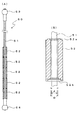
ワイヤー50は、ワイヤー本体51と、このワイヤー本体51に設けられた複数のカラー52とを備えている。ワイヤー本体51には、種結晶ならびにインゴット13の回転振れや耐熱等を考慮し、タングステンなどの材料からなる線材を捩り込んだもの(ストランド)が使用されている。
The
また、図2に示すようにワイヤー本体51の両端には、ボールジョイント方式の嵌め合いにより巻取器30並びに連結部材31と連結される連結部53,54がそれぞれ設けられている。これにより、例えば、連結部材31には、図3に示すように、連結部54が嵌め合わされる際の挿入部31aが形成されている。
As shown in FIG. 2, connecting portions 53 and 54 connected to the
連結部54はステンレス製のかしめ部54aをかしめることによりワイヤー本体51に取り付けられている。連結部材31にはかしめ部54aのみが接触し、ワイヤー本体51は連結部材31には直接接触しないため、ワイヤー本体51の磨耗を防ぐことができる。また、連結部材31内にワイヤー本体51が露出されることがないため、挿入部31aから連結部材31内に侵入する雰囲気ガスにワイヤー本体51が晒されることもなく、ワイヤー本体の酸化消耗を防止し、ワイヤーの劣化を低減させることができる。 The connecting portion 54 is attached to the wire body 51 by caulking a stainless caulking portion 54a. Since only the caulking portion 54a contacts the connecting member 31 and the wire main body 51 does not directly contact the connecting member 31, wear of the wire main body 51 can be prevented. Moreover, since the wire main body 51 is not exposed in the connection member 31, the wire main body 51 is not exposed to the atmospheric gas which invades into the connection member 31 from the insertion portion 31a, and the oxidation of the wire main body is prevented. And deterioration of a wire can be reduced.
カラー52は、ステンレスやモリブデン、タングステン等により円筒形状に形成されており、図2(B)に示すように、その両端には隣接する上下で互いに隙無く連結するための雌雄の異なる係合部としての凸部52aと凹部52bとが形成されている。このように、複数に分割されたカラーに雌雄の異なる係合部を設けることにより、互いに上下方向で隣接するもの同士の隙間の発生を防止することができ、カラーの隙間からの輻射熱や酸化物の侵入を防止することができる。 The collar 52 is formed in a cylindrical shape using stainless steel, molybdenum, tungsten, or the like, and as shown in FIG. The convex part 52a and the recessed part 52b are formed. In this way, by providing the male and female engaging portions in the collar divided into a plurality of parts, it is possible to prevent the generation of gaps between those adjacent to each other in the vertical direction. Can be prevented from entering.
また、カラー52は、ワイヤー本体51の直径dに対して内径Dの方が大径とされている。この際、内径Dと直径dとの差は、ワイヤー本体51の経年的劣化により、その芯材(図示せず)が切断されたり線材の捩りが戻った場合のように、部分的にワイヤー本体51の直径が膨らむことを許容している。 The collar 52 has a larger inner diameter D than the diameter d of the wire body 51. At this time, the difference between the inner diameter D and the diameter d is partially due to the aging of the wire body 51, such as when the core material (not shown) is cut or the twist of the wire is restored. The diameter of 51 is allowed to swell.
このように、カラーの内径をワイヤーの直径よりも大径としたことにより、芯のあるワイヤーの場合に、側面のワイヤーに外傷がなくても芯のワイヤーが破断に近い状態にある時には側面のワイヤーの直径がカラー内径の範囲内で大きくなり、カラーを上下に動かすことにより、その摩擦力によりふくらみを検出でき、ワイヤー破断までに至るのを防止できる。 Thus, by making the inner diameter of the collar larger than the diameter of the wire, in the case of a cored wire, when the core wire is in a state close to breaking even if the side wire is not damaged, the side surface The diameter of the wire increases within the range of the inner diameter of the collar, and when the collar is moved up and down, the bulge can be detected by the frictional force, and the wire can be prevented from breaking.
例えば、定期的な点検時やホッパーと種結晶との交換時において、カラー52をワイヤー本体51の軸線に沿って移動させ、ワイヤー本体51に膨らみが発生していない場合にはカラー52の移動が滑らかに行われ、ワイヤー本体51に膨らみが発生している場合にはカラー52の移動が阻害されるため、ワイヤー本体51の劣化を容易に確認することができる。もちろん、カラー52が上下動可能なことにより、ワイヤー本体51の断線や変形を目視により確認できることは言うまでもない。 For example, the collar 52 is moved along the axis of the wire body 51 during periodic inspections or when the hopper and the seed crystal are exchanged. If the wire body 51 is not bulged, the collar 52 is moved. When the wire body 51 is swelled smoothly, the movement of the collar 52 is hindered, so that the deterioration of the wire body 51 can be easily confirmed. Of course, since the collar 52 can be moved up and down, it is needless to say that disconnection and deformation of the wire body 51 can be visually confirmed.
また、引き上げるインゴット33の結晶長が長くなってもカラーが障害とならないように、カラー52の外径寸法は、巻き上げ部の空間を通過することができるサイズであることが好ましい。 The outer diameter of the collar 52 is preferably a size that can pass through the space of the winding portion so that the collar does not become an obstacle even if the crystal length of the ingot 33 to be pulled up becomes long.
このような構成において、原料となる素材を内部に装填したホッパーを装着した状態でワイヤー50を下降させてルツボ24内に素材を落下投入する。素材の投入後ホッパーを上昇させて、一旦ゲートバルブ34によりプルチャンバ23を上下で隔絶する(実質的にはチャンバ22の炉内とプルチャンバ23の内部とを隔絶する)。その状態でプルチャンバ23内にガスを封入する事により大気開放を可能とし、ホッパーを連結部材31から取り外した後に、新たに種結晶を装着したシードホルダ32を連結部材31に装着する。
In such a configuration, the material is dropped into the
その後、ゲートバルブ34を開放して種結晶をルツボ24のシリコン融液28の液面に接触させ、ルツボ24を回転させつつ(ワイヤー50を同時に同方向または逆方向に回転させても良い)ワイヤー50を巻取器30で巻き取ってシードホルダ32を引き上げることで単結晶のインゴット33が成長する。
Thereafter, the
この際、図1(A)に示すようにシードホルダ32が着液位置にある状態では、ワイヤー本体51の先端部分はある程度の範囲でカラー52により覆われていることにより、ヒータ24からの輻射熱やシリコン融液28からの酸化物との反応によるワイヤー50の局所的な劣化を低減することができる。より具体的には、着液位置にあるときにカラー52により覆われているワイヤー本体51の先端が700℃未満になるようにする。
At this time, as shown in FIG. 1A, in the state where the
また、シードホルダ32が着液位置にある状態において、ワイヤー本体51がカラー52から露出している部分、特に、カラー52の近部でカラー52から露出している部分が、炉内温度700℃前後のエリアBとエリアCとの境界付近からエリアC内に位置するように、カラー52の長さを調節する。より具体的には、着液位置にあるときにワイヤー本体51の露出部分が700℃未満になるように、カラー52の長さを設定する。
Further, in the state where the
このように、カラー52により覆うワイヤー本体51の範囲を、チャンバ22の炉内高さを考慮したうえでその高温雰囲気下に相当する範囲とすることにより、装置本体の設計変更をすることなく既存の連結部材31並びにシードホルダ32を使用したままワイヤー本体51の酸化に伴う劣化を低減することができる。
As described above, the range of the wire body 51 covered with the collar 52 is set to a range corresponding to the high temperature atmosphere in consideration of the height of the
特に、酸化物との反応が激しく始まる温度である700℃未満にワイヤーを保つことにより、ワイヤーの酸化を遅らせ、ワイヤーの局所的な劣化を低減することができる。 In particular, by keeping the wire below 700 ° C., which is the temperature at which the reaction with the oxide starts intensely, it is possible to delay the oxidation of the wire and reduce local deterioration of the wire.
上記の実施例ではインゴットの引き上げに用いられるワイヤーについて説明を行ったが、同じようにチャンバ内で用いられるワイヤーであれば、本発明のカラーの概念は同様にして適用可能であり、本発明はインゴットの引上げに限ったものではない。 In the above embodiment, the wire used for pulling up the ingot has been described. However, as long as the wire is used in the chamber, the concept of the color of the present invention can be similarly applied, and the present invention It is not limited to raising ingots.
図4は、本発明の半導体インゴット製造装置の実施例2を示し、(A)はシードホルダが着液位置にある状態の半導体インゴット製造装置の説明図、(B)はシードホルダが上端位置にある状態の半導体インゴット製造装置の説明図である。 4A and 4B show a second embodiment of the semiconductor ingot manufacturing apparatus according to the present invention, in which FIG. 4A is an explanatory view of the semiconductor ingot manufacturing apparatus in a state where the seed holder is in the liquid landing position, and FIG. It is explanatory drawing of the semiconductor ingot manufacturing apparatus of a certain state.
尚、この図4に示した実施例2の半導体インゴット製造装置21は、上述した実施例1とはワイヤーの先端に設けられた連結部材とこの連結部材に装着されたシードホルダとが異なるのみなので、その他の構成部材には上記実施例1の図1と同一の符号を付してその説明を省略する。 The semiconductor ingot manufacturing apparatus 21 of Example 2 shown in FIG. 4 is different from Example 1 described above only in the connecting member provided at the tip of the wire and the seed holder attached to the connecting member. The other constituent members are denoted by the same reference numerals as those in FIG.
シードホルダ32はカーボン等から形成されており、着液位置にあるときにワイヤー29の先端近傍の露出部分がチャンバ22の炉内上方、即ち、少なくとも炉内高温雰囲気下でエリアBとエリアCとの境界付近からエリアC内に位置するように長さが設定されている。より具体的には、着液位置にあるときにワイヤー29の先端近傍のワイヤー露出部分が700℃未満になるように長さを設定する。
The
また、リチャージ引上げの場合、シードホルダ32の長さの最長は、インゴット33を吊り上げた上端位置にあるときに、そのインゴット33の下端がゲートバルブ34よりも上方に位置するように設定されている。この際、プルチャンバ23の設計変更(高さ変更やシール部品35並びに回転伝達部品36の大径化)は無いようにすることが好ましい。
In the case of recharge pulling, the longest length of the
このような構成において、原料となる素材を内部に装填したホッパーを装着した状態でワイヤー29を下降させてルツボ24内に素材を落下投入する。素材の投入後ホッパーを上昇させて、一旦ゲートバルブ34によりプルチャンバ23を上下で隔絶する。ホッパーを連結部材31から取り外した後に、新たに種結晶を装着したシードホルダ32を連結部材31に装着する。
In such a configuration, the
ルツボ24内の素材をヒータ25により溶融させ、ゲートバルブ34を開放し、ワイヤー29を着液位置まで下降させて種結晶をルツボ24のシリコン融液28の液面に接触させる。ルツボ24を回転させつつ(ワイヤー29を同時に同方向または逆方向に回転させても良い)ワイヤー29を巻取器30で巻き取ってシードホルダ32を引き上げることで、単結晶のインゴット33が成長する。
The material in the
この際図4(A)に示すように、シードホルダ32が着液位置にある状態では、ワイヤー29の先端近傍のワイヤー露出部分、即ち、連結部材31の近部で連結部材31から露出している部分は、炉内温度700℃前後のエリアBとエリアCとの境界付近からエリアC内に位置しているため、ヒータ25からの輻射熱やシリコン融液28からの酸化物との反応によるワイヤー29の局所的な劣化を低減することができる。
At this time, as shown in FIG. 4A, when the
特に、タングステンにおいて酸化物との反応が激しく始まる温度である700℃未満の雰囲気に、ワイヤー先端の露出部分を位置させることにより、ワイヤーの酸化を遅らせ、ワイヤーの局所的な劣化を低減することができる。 In particular, it is possible to delay the oxidation of the wire and reduce the local deterioration of the wire by positioning the exposed portion of the tip of the wire in an atmosphere of less than 700 ° C., which is the temperature at which the reaction with the oxide starts intensely in tungsten. it can.
図5は、本発明の半導体インゴット製造装置の実施例3を示し、(A)はシードホルダが着液位置にある状態の半導体インゴット製造装置の説明図、(B)はシードホルダが上端位置にある状態の半導体インゴット製造装置の説明図である。 5A and 5B show a third embodiment of the semiconductor ingot manufacturing apparatus according to the present invention, in which FIG. 5A is an explanatory diagram of the semiconductor ingot manufacturing apparatus in a state where the seed holder is in the liquid landing position, and FIG. 5B is the top view of the seed holder. It is explanatory drawing of the semiconductor ingot manufacturing apparatus of a certain state.
尚、この図5に示した実施例3の半導体インゴット製造装置21は、上述した実施例1とはワイヤー29の先端に設けられた連結部材とこの連結部材に装着されたシードホルダとが異なるのみなので、その他の構成部材には上記実施例1の図1と同一の符号を付してその説明を省略する。
In addition, the semiconductor ingot manufacturing apparatus 21 of Example 3 shown in FIG. 5 differs from Example 1 described above only in the connecting member provided at the tip of the
連結部材41は、ワイヤー29に着脱可能に設けられていると共にシードホルダ42を着脱可能に保持している。また、連結部材41は、シートホルダ42が着液位置にあるときにワイヤー29の先端がチャンバ22の炉内上方、即ち、少なくとも炉内高温雰囲気下でエリアBとエリアCとの境界付近からエリアC内に位置するように長さが設定されている。より具体的には、着液位置にあるときにワイヤー29の先端近傍のワイヤー露出部分が700℃未満になるように長さを設定する。
The connecting member 41 is detachably provided on the
また、連結部材41の長さの最長は、インゴット33を吊り上げた上端位置にあるときに、そのインゴット33の下端がゲートバルブ34よりも上方に位置するように設定されている。この際、プルチャンバ23の設計変更(高さ変更やシール部品35並びに回転伝達部品36の大径化)は無いようにすることが好ましい。
The longest length of the connecting member 41 is set so that the lower end of the ingot 33 is positioned above the
このような構成においても、ゲートバルブ34を開放して種結晶をルツボ24のシリコン融液28の液面に接触させ、ルツボ24を回転させつつ(ワイヤー29を同時に同方向または逆方向に回転させても良い)ワイヤー29を巻取器30で巻き取ってシードホルダ42を引き上げることで、単結晶のインゴット33が成長する。
Even in such a configuration, the
この際図5(A)に示すように、シードホルダ42が着液位置にある状態では、ワイヤー29の先端近傍のワイヤー露出部分、即ち、連結部材41の近部で連結部材41から露出している部分は、炉内温度700℃前後のエリアBとエリアCとの境界付近からエリアC内に位置しているため、ヒータ25からの輻射熱やシリコン融液28からの酸化物との反応によるワイヤー29の局所的な劣化を低減することができる。
At this time, as shown in FIG. 5A, when the seed holder 42 is in the liquid landing position, the wire exposed portion near the tip of the
特に、タングステンにおいて酸化物との反応が激しく始まる温度である700℃未満の雰囲気に、ワイヤー先端の露出部分を位置させることにより、ワイヤーの酸化を遅らせ、ワイヤーの局所的な劣化を低減することができる。 In particular, it is possible to delay the oxidation of the wire and reduce the local deterioration of the wire by positioning the exposed portion of the tip of the wire in an atmosphere of less than 700 ° C., which is the temperature at which the reaction with the oxide starts intensely in tungsten. it can.
尚、上記の実施例2または3においては、上記実施例1に開示した構成を併用しても良い。また、上記実施例1乃至3において、ワイヤーとシードホルダを結合するために連結部材を用いているが、本願において連結部材とは、必ずしもシードホルダと別部材である必要はなく、シードホルダの一部分でワイヤーとの結合の役割を果たす部位も含む。 In the second or third embodiment, the configuration disclosed in the first embodiment may be used in combination. In the first to third embodiments, a connecting member is used to connect the wire and the seed holder. However, in the present application, the connecting member is not necessarily a separate member from the seed holder, and a part of the seed holder. It also includes a site that plays a role of bonding with the wire.
ワイヤーの高温に晒される領域にカラーを設けることは、上記の実施例1に示したインゴットの引き上げに用いられるワイヤーに限定されるものではなく、炉内に配置される如何なる目的のワイヤーに対しても適用することができる。
また、上記の実施例1乃至3の説明においては、単結晶インゴットの製造を例に説明しているが、本発明は単結晶インゴット以外にも化合物半導体のインゴットやその他のインゴットについても適用可能である。
The provision of the collar in the region exposed to the high temperature of the wire is not limited to the wire used for pulling up the ingot shown in the first embodiment, but for any desired wire placed in the furnace. Can also be applied.
In the description of Examples 1 to 3 described above, the manufacture of a single crystal ingot is described as an example. However, the present invention can be applied to ingots of compound semiconductors and other ingots in addition to the single crystal ingot. is there.
1…半導体インゴット製造装置
2…チャンバ
3…プルチャンバ
4…ルツボ
5…ヒータ
6…断熱材
7…回転軸
8…シリコン融液
9…ワイヤー
10…巻取器
11…連結部材
12…シードホルダ
13…インゴット
14…ゲートバルブ
21…半導体インゴット製造装置
22…チャンバ
23…プルチャンバ
24…ルツボ
25…ヒータ
26…断熱材
27…回転軸
28…シリコン融液
29…ワイヤー
30…巻取器
31…連結部材 31a…挿入部
32…シードホルダ
33…インゴット
34…ゲートバルブ
35…シール部品
36…回転伝達部品
41…連結部材
42…シードホルダ
50…ワイヤー
51…ワイヤー本体
52…カラー 52a…凸部 52b…凹部
53…連結部
54…連結部 54a…かしめ部。
DESCRIPTION OF
Claims (6)
前記ワイヤーの少なくとも高温にさらされる領域を、カラーで覆ったことを特徴とする半導体単結晶製造装置。 In a semiconductor single crystal manufacturing apparatus comprising a chamber provided with a crucible filled with a melt in a furnace, a heater for heating the crucible, and a wire provided in the chamber,
An apparatus for producing a semiconductor single crystal, wherein at least a region of the wire exposed to a high temperature is covered with a collar.
前記シードホルダは前記チャンバ内で昇降可能であり、
前記シードホルダ若しくは前記連結部材の少なくとも一方の長さを、前記シードホルダに種結晶を取り付け、該種結晶が融液に着液する位置にあるとき、前記ワイヤーの先端近傍で前記連結部材から露出している部分が前記炉内の高温雰囲気下で所定温度未満の範囲に位置する長さとしたことを特徴とする請求項1に記載の半導体単結晶製造装置。 The wire includes a connecting member at the tip, and a seed holder is suspended through the connecting member,
The seed holder can be raised and lowered in the chamber,
The length of at least one of the seed holder or the connecting member is exposed from the connecting member in the vicinity of the tip of the wire when a seed crystal is attached to the seed holder and the seed crystal is in a position where the seed crystal reaches the melt. semiconductor single crystal manufacturing apparatus according to claim 1, part you are is characterized in that the length located in the range of lower than the predetermined temperature in a high temperature atmosphere in the furnace.
Priority Applications (5)
| Application Number | Priority Date | Filing Date | Title |
|---|---|---|---|
| JP2003353962A JP4362760B2 (en) | 2003-10-14 | 2003-10-14 | Semiconductor single crystal manufacturing equipment |
| TW093130512A TWI261076B (en) | 2003-10-14 | 2004-10-08 | Apparatus for manufacturing semiconductor single crystal |
| US10/575,481 US7413609B2 (en) | 2003-10-14 | 2004-10-13 | Semiconductor single crystal manufacturing apparatus |
| PCT/JP2004/015050 WO2005035839A1 (en) | 2003-10-14 | 2004-10-13 | Semiconductor single crystal manufacturing apparatus |
| DE112004001947.8T DE112004001947B4 (en) | 2003-10-14 | 2004-10-13 | Device for producing a monocrystal semiconductor |
Applications Claiming Priority (1)
| Application Number | Priority Date | Filing Date | Title |
|---|---|---|---|
| JP2003353962A JP4362760B2 (en) | 2003-10-14 | 2003-10-14 | Semiconductor single crystal manufacturing equipment |
Publications (3)
| Publication Number | Publication Date |
|---|---|
| JP2005119891A JP2005119891A (en) | 2005-05-12 |
| JP2005119891A5 JP2005119891A5 (en) | 2006-11-09 |
| JP4362760B2 true JP4362760B2 (en) | 2009-11-11 |
Family
ID=34431176
Family Applications (1)
| Application Number | Title | Priority Date | Filing Date |
|---|---|---|---|
| JP2003353962A Expired - Lifetime JP4362760B2 (en) | 2003-10-14 | 2003-10-14 | Semiconductor single crystal manufacturing equipment |
Country Status (5)
| Country | Link |
|---|---|
| US (1) | US7413609B2 (en) |
| JP (1) | JP4362760B2 (en) |
| DE (1) | DE112004001947B4 (en) |
| TW (1) | TWI261076B (en) |
| WO (1) | WO2005035839A1 (en) |
Families Citing this family (2)
| Publication number | Priority date | Publication date | Assignee | Title |
|---|---|---|---|---|
| JP2010180072A (en) * | 2009-02-03 | 2010-08-19 | Shin Etsu Handotai Co Ltd | Apparatus for producing single crystal |
| CN113061974B (en) * | 2021-03-23 | 2022-02-15 | 浙江晶阳机电股份有限公司 | Vacuum straight pulling furnace production mechanism and straightening and crystal taking method thereof |
Family Cites Families (12)
| Publication number | Priority date | Publication date | Assignee | Title |
|---|---|---|---|---|
| JPS5928560A (en) | 1982-08-06 | 1984-02-15 | Nippon Steel Corp | Stainless steel excellent in surface properties and corrosion resistance |
| JPS5928560U (en) * | 1982-08-12 | 1984-02-22 | 東芝機械株式会社 | Seed holder support device for single crystal pulling machine |
| DE69017642T2 (en) * | 1989-12-22 | 1995-07-06 | Shinetsu Handotai Kk | Device for the production of single crystals according to the Czochralski process. |
| JPH048382A (en) * | 1990-04-26 | 1992-01-13 | Kazuo Saito | Footwear type game vehicle |
| JP3526927B2 (en) * | 1994-10-14 | 2004-05-17 | コマツ電子金属株式会社 | Semiconductor single crystal pulling equipment |
| JP3109564B2 (en) | 1995-03-27 | 2000-11-20 | 大倉電気株式会社 | Weight measuring device for grown crystal |
| JP2940439B2 (en) * | 1995-06-10 | 1999-08-25 | 信越半導体株式会社 | Single crystal pulling device |
| JP2949571B2 (en) | 1996-01-31 | 1999-09-13 | 住友金属工業株式会社 | Single crystal growth equipment |
| JP3596226B2 (en) * | 1997-03-17 | 2004-12-02 | 信越半導体株式会社 | Single crystal holding device |
| JP3964002B2 (en) * | 1997-06-02 | 2007-08-22 | Sumco Techxiv株式会社 | Single crystal holding apparatus and single crystal holding method |
| US6183556B1 (en) * | 1998-10-06 | 2001-02-06 | Seh-America, Inc. | Insulating and warming shield for a seed crystal and seed chuck |
| US6340391B1 (en) * | 1998-12-28 | 2002-01-22 | Shin-Etsu Handotai Co. | Method for producing single crystal and pulling device |
-
2003
- 2003-10-14 JP JP2003353962A patent/JP4362760B2/en not_active Expired - Lifetime
-
2004
- 2004-10-08 TW TW093130512A patent/TWI261076B/en active
- 2004-10-13 US US10/575,481 patent/US7413609B2/en active Active
- 2004-10-13 DE DE112004001947.8T patent/DE112004001947B4/en active Active
- 2004-10-13 WO PCT/JP2004/015050 patent/WO2005035839A1/en active Application Filing
Also Published As
| Publication number | Publication date |
|---|---|
| DE112004001947T5 (en) | 2006-08-24 |
| US20070051303A1 (en) | 2007-03-08 |
| WO2005035839A1 (en) | 2005-04-21 |
| DE112004001947B4 (en) | 2017-02-09 |
| JP2005119891A (en) | 2005-05-12 |
| TWI261076B (en) | 2006-09-01 |
| TW200516179A (en) | 2005-05-16 |
| US7413609B2 (en) | 2008-08-19 |
Similar Documents
| Publication | Publication Date | Title |
|---|---|---|
| JP5413354B2 (en) | Silicon single crystal pulling apparatus and silicon single crystal manufacturing method | |
| JP2004511410A (en) | Heat shield assembly for crystal puller | |
| JP2008019125A (en) | Method of melting semiconductor wafer base material and method of growing semiconductor wafer crystal | |
| KR100679135B1 (en) | Thermal shield member of silicon single crystal pulling system | |
| JP4362760B2 (en) | Semiconductor single crystal manufacturing equipment | |
| JP3670493B2 (en) | Single crystal pulling device | |
| JP2006315869A (en) | Method for manufacturing nitrogen-doped silicon single crystal | |
| JP3011114B2 (en) | Silicon melting crucible | |
| JP4672579B2 (en) | Method for recharging solid raw materials | |
| JP4611076B2 (en) | β-Ga2O3 single crystal manufacturing equipment | |
| JP2004522684A (en) | Crystal puller and method for growing single crystal semiconductor material | |
| JP2012106870A (en) | Method of growing crystal | |
| JP6471700B2 (en) | Method for melting silicon raw material using recharge device | |
| JP4563951B2 (en) | Solid material recharging equipment | |
| JP4272449B2 (en) | Single crystal pulling method | |
| JP2007254162A (en) | Single crystal manufacturing device and recharge method | |
| WO2022091635A1 (en) | Single crystal production device | |
| JPH09183687A (en) | Method for elevating flow regulating cylinder of apparatus for pulling up single crystal and flow regulating cylinder elevating mechanism for apparatus for pulling up single crystal | |
| JPH11255575A (en) | Device for pulling single crystal and its cooling | |
| JP2002255684A (en) | Manufacturing method of silicone monocrystal ingot | |
| JP3557872B2 (en) | Silicon single crystal growth equipment | |
| JPH06144986A (en) | Apparatus and method for production of semiconductor single crystal | |
| JP2010006657A (en) | Silicon single crystal production apparatus and silicon single crystal production method | |
| KR100872806B1 (en) | Apparatus of manufacturing silicon single crystal ingot | |
| JP2008063205A (en) | Recharge device of solid raw material and recharge method using the same |
Legal Events
| Date | Code | Title | Description |
|---|---|---|---|
| A521 | Request for written amendment filed |
Free format text: JAPANESE INTERMEDIATE CODE: A523 Effective date: 20060927 |
|
| A621 | Written request for application examination |
Free format text: JAPANESE INTERMEDIATE CODE: A621 Effective date: 20060927 |
|
| TRDD | Decision of grant or rejection written | ||
| A01 | Written decision to grant a patent or to grant a registration (utility model) |
Free format text: JAPANESE INTERMEDIATE CODE: A01 Effective date: 20090804 |
|
| A01 | Written decision to grant a patent or to grant a registration (utility model) |
Free format text: JAPANESE INTERMEDIATE CODE: A01 |
|
| A61 | First payment of annual fees (during grant procedure) |
Free format text: JAPANESE INTERMEDIATE CODE: A61 Effective date: 20090805 |
|
| FPAY | Renewal fee payment (event date is renewal date of database) |
Free format text: PAYMENT UNTIL: 20120828 Year of fee payment: 3 |
|
| R150 | Certificate of patent or registration of utility model |
Ref document number: 4362760 Country of ref document: JP Free format text: JAPANESE INTERMEDIATE CODE: R150 Free format text: JAPANESE INTERMEDIATE CODE: R150 |
|
| FPAY | Renewal fee payment (event date is renewal date of database) |
Free format text: PAYMENT UNTIL: 20120828 Year of fee payment: 3 |
|
| FPAY | Renewal fee payment (event date is renewal date of database) |
Free format text: PAYMENT UNTIL: 20130828 Year of fee payment: 4 |
|
| R250 | Receipt of annual fees |
Free format text: JAPANESE INTERMEDIATE CODE: R250 |
|
| R250 | Receipt of annual fees |
Free format text: JAPANESE INTERMEDIATE CODE: R250 |
|
| R250 | Receipt of annual fees |
Free format text: JAPANESE INTERMEDIATE CODE: R250 |
|
| R250 | Receipt of annual fees |
Free format text: JAPANESE INTERMEDIATE CODE: R250 |
|
| R250 | Receipt of annual fees |
Free format text: JAPANESE INTERMEDIATE CODE: R250 |
|
| R250 | Receipt of annual fees |
Free format text: JAPANESE INTERMEDIATE CODE: R250 |
|
| R250 | Receipt of annual fees |
Free format text: JAPANESE INTERMEDIATE CODE: R250 |
|
| R250 | Receipt of annual fees |
Free format text: JAPANESE INTERMEDIATE CODE: R250 |
|
| R250 | Receipt of annual fees |
Free format text: JAPANESE INTERMEDIATE CODE: R250 |
|
| R250 | Receipt of annual fees |
Free format text: JAPANESE INTERMEDIATE CODE: R250 |
|
| R250 | Receipt of annual fees |
Free format text: JAPANESE INTERMEDIATE CODE: R250 |
|
| R250 | Receipt of annual fees |
Free format text: JAPANESE INTERMEDIATE CODE: R250 |
|
| EXPY | Cancellation because of completion of term |