JP4357438B2 - 半導体光変調器 - Google Patents
半導体光変調器 Download PDFInfo
- Publication number
- JP4357438B2 JP4357438B2 JP2005064497A JP2005064497A JP4357438B2 JP 4357438 B2 JP4357438 B2 JP 4357438B2 JP 2005064497 A JP2005064497 A JP 2005064497A JP 2005064497 A JP2005064497 A JP 2005064497A JP 4357438 B2 JP4357438 B2 JP 4357438B2
- Authority
- JP
- Japan
- Prior art keywords
- layer
- semiconductor
- semiconductor optical
- optical modulator
- modulator
- Prior art date
- Legal status (The legal status is an assumption and is not a legal conclusion. Google has not performed a legal analysis and makes no representation as to the accuracy of the status listed.)
- Expired - Fee Related
Links
Images


Landscapes
- Optical Modulation, Optical Deflection, Nonlinear Optics, Optical Demodulation, Optical Logic Elements (AREA)
Description
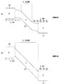
2 空乏領域
3 正孔
10、10a、10b n型半導体クラッド層
20 ノンドープ層/光導波層
30 p型半導体クラッド層
40、40a、40b、50 中間層
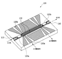
100 半導体変調器
110 入力導波路
120a 光分岐器
120b 光合波器
130 位相変調導波路
140 出力光導波路
150a、150b 高周波電界印加線路
Claims (8)
- 半導体光導波層と、n型半導体クラッド層とを備えた導波路を有する半導体光変調器において、
前記半導体光導波層と前記n型半導体クラッド層との間にあって、無電界状態で前記n型半導体クラッド層から前記半導体光導波層への多数キャリアの拡散を防ぐポテンシャル障壁となる中間層を備えたことを特徴とする半導体光変調器。 - 請求項1に記載の半導体光変調器において、
前記半導体光導波層は、ノンドープInGaAsP層またはノンドープInGaAlAs層からなり、
前記n型半導体クラッド層は、n−InP層からなることを特徴とする半導体光変調器。 - 請求項2に記載の半導体光変調器において、
前記中間層は、InAlAsを含むことを特徴とする半導体光変調器。 - 電気光学効果を有する半導体光導波層と、該半導体光導波層の上下を挟む第1のクラッド層と、該第1のクラッド層の上下を挟む第2のクラッド層を備えた半導体へテロ構造の光導波路を有する半導体光変調器において、
前記第2のクラッド層の少なくとも一方は、n型半導体層で構成され、
前記n型半導体層に接する前記第1のクラッド層は、無電界状態で前記第2のクラッド層から前記半導体光導波層への多数キャリアの拡散を防ぐポテンシャル障壁となることを特徴とする半導体光変調器。 - 請求項4に記載の半導体光変調器において、
前記第2のクラッド層は、ともにn型半導体層で構成されたことを特徴とする半導体光変調器。 - 請求項5に記載の半導体変調器において、
前記半導体光導波層は、ノンドープInGaAsP層またはノンドープInGaAlAs層からなり、
前記第2のクラッド層は、n−InP層からなることを特徴とする半導体光変調器。 - 請求項6に記載の半導体光変調器において、
前記第1のクラッド層は、InAlAsを含むことを特徴とする半導体光変調器。 - 請求項1ないし7のいずれかに記載の半導体光変調器であって、
マッハツェンダ干渉計により構成されたことを特徴とする半導体光変調器。
Priority Applications (1)
| Application Number | Priority Date | Filing Date | Title |
|---|---|---|---|
| JP2005064497A JP4357438B2 (ja) | 2005-03-08 | 2005-03-08 | 半導体光変調器 |
Applications Claiming Priority (1)
| Application Number | Priority Date | Filing Date | Title |
|---|---|---|---|
| JP2005064497A JP4357438B2 (ja) | 2005-03-08 | 2005-03-08 | 半導体光変調器 |
Publications (2)
| Publication Number | Publication Date |
|---|---|
| JP2006251087A JP2006251087A (ja) | 2006-09-21 |
| JP4357438B2 true JP4357438B2 (ja) | 2009-11-04 |
Family
ID=37091705
Family Applications (1)
| Application Number | Title | Priority Date | Filing Date |
|---|---|---|---|
| JP2005064497A Expired - Fee Related JP4357438B2 (ja) | 2005-03-08 | 2005-03-08 | 半導体光変調器 |
Country Status (1)
| Country | Link |
|---|---|
| JP (1) | JP4357438B2 (ja) |
Families Citing this family (5)
| Publication number | Priority date | Publication date | Assignee | Title |
|---|---|---|---|---|
| JP4750764B2 (ja) * | 2007-08-02 | 2011-08-17 | 日本電信電話株式会社 | 半導体光変調器 |
| US8300991B2 (en) * | 2008-03-28 | 2012-10-30 | Nec Corporation | Waveguide-type semiconductor optical modulator and method for manufacturing the same |
| JP5262960B2 (ja) * | 2009-04-28 | 2013-08-14 | 日本電気株式会社 | 半導体マッハツェンダー光変調器及びその製造方法、半導体光集積素子及びその製造方法 |
| JP5338456B2 (ja) * | 2009-04-28 | 2013-11-13 | 日本電気株式会社 | 半導体マッハツェンダー光変調器及びその製造方法、半導体光集積素子及びその製造方法 |
| JP2012083499A (ja) | 2010-10-08 | 2012-04-26 | Fujitsu Optical Components Ltd | 光変調装置及び光変調方法 |
-
2005
- 2005-03-08 JP JP2005064497A patent/JP4357438B2/ja not_active Expired - Fee Related
Also Published As
| Publication number | Publication date |
|---|---|
| JP2006251087A (ja) | 2006-09-21 |
Similar Documents
| Publication | Publication Date | Title |
|---|---|---|
| US6647158B2 (en) | Optical modulator using simultaneous push-pull drive of linear and quadratic electro-optic effects | |
| CN102033333B (zh) | 半导体光调制器 | |
| EP2458433B1 (en) | Optical modulator and manufacturing method of the optical modulator | |
| US7355778B2 (en) | Semiconductor optical modulator | |
| US5694504A (en) | Semiconductor modulator with a π shift | |
| JP2606079B2 (ja) | 光半導体素子 | |
| JP2002131714A (ja) | 電界吸収型光変調器付き半導体レーザ及びその駆動回路並びに半導体レーザ装置 | |
| US5655034A (en) | Mach-Zehnder type modulator and method of driving the same | |
| Tsuzuki et al. | A 40-Gb/s InGaAlAs-InAlAs MQW nin Mach-Zehnder modulator with a drive voltage of 2.3 V | |
| JP4357438B2 (ja) | 半導体光変調器 | |
| JP4494257B2 (ja) | 光変調器 | |
| Akiyama et al. | Low-chirp 10 Gbit/s InP-based Mach-Zehnder modulator driven by 1.2 V single electrical signal | |
| JP2014191218A (ja) | 光変調器 | |
| CN100370317C (zh) | 半导体光调制器 | |
| JP2018092100A (ja) | 光送信器 | |
| JP5906210B2 (ja) | 光変調器 | |
| JP2016114712A (ja) | 半導体マッハツェンダー光変調器 | |
| JP6151958B2 (ja) | 光変調素子および光変調素子の駆動方法 | |
| US20050141072A1 (en) | Electroabsorption modulator with two sections | |
| Tsuzuki et al. | InP‐based n‐i‐n Mach‐Zehnder optical modulator | |
| Tsuzuki et al. | Low driving voltage 40 Gbit/s nin Mach-Zehnder modulator fabricated on InP substrate | |
| Chen et al. | Hybrid silicon evanescent modulators | |
| Yamada et al. | High-mesa Ridge/BH hybrid structure optical gating device based on cross-absorption modulation of electro-absorption modulator | |
| JPH09311303A (ja) | 半導体光変調器、光通信用モジュール、及び光通信システム | |
| Westergren et al. | Compact modulators for fiber-optical communications at 100Gb/s and above |
Legal Events
| Date | Code | Title | Description |
|---|---|---|---|
| A621 | Written request for application examination |
Free format text: JAPANESE INTERMEDIATE CODE: A621 Effective date: 20070221 |
|
| A977 | Report on retrieval |
Free format text: JAPANESE INTERMEDIATE CODE: A971007 Effective date: 20080509 |
|
| A131 | Notification of reasons for refusal |
Free format text: JAPANESE INTERMEDIATE CODE: A131 Effective date: 20080523 |
|
| A521 | Written amendment |
Free format text: JAPANESE INTERMEDIATE CODE: A523 Effective date: 20080717 |
|
| TRDD | Decision of grant or rejection written | ||
| A01 | Written decision to grant a patent or to grant a registration (utility model) |
Free format text: JAPANESE INTERMEDIATE CODE: A01 Effective date: 20090728 |
|
| A01 | Written decision to grant a patent or to grant a registration (utility model) |
Free format text: JAPANESE INTERMEDIATE CODE: A01 |
|
| A61 | First payment of annual fees (during grant procedure) |
Free format text: JAPANESE INTERMEDIATE CODE: A61 Effective date: 20090804 |
|
| FPAY | Renewal fee payment (event date is renewal date of database) |
Free format text: PAYMENT UNTIL: 20120814 Year of fee payment: 3 |
|
| R151 | Written notification of patent or utility model registration |
Ref document number: 4357438 Country of ref document: JP Free format text: JAPANESE INTERMEDIATE CODE: R151 |
|
| FPAY | Renewal fee payment (event date is renewal date of database) |
Free format text: PAYMENT UNTIL: 20120814 Year of fee payment: 3 |
|
| FPAY | Renewal fee payment (event date is renewal date of database) |
Free format text: PAYMENT UNTIL: 20130814 Year of fee payment: 4 |
|
| S531 | Written request for registration of change of domicile |
Free format text: JAPANESE INTERMEDIATE CODE: R313531 |
|
| R350 | Written notification of registration of transfer |
Free format text: JAPANESE INTERMEDIATE CODE: R350 |
|
| LAPS | Cancellation because of no payment of annual fees |