JP4357117B2 - Optical system, especially microlithographic projection exposure apparatus - Google Patents
Optical system, especially microlithographic projection exposure apparatus Download PDFInfo
- Publication number
- JP4357117B2 JP4357117B2 JP2000556280A JP2000556280A JP4357117B2 JP 4357117 B2 JP4357117 B2 JP 4357117B2 JP 2000556280 A JP2000556280 A JP 2000556280A JP 2000556280 A JP2000556280 A JP 2000556280A JP 4357117 B2 JP4357117 B2 JP 4357117B2
- Authority
- JP
- Japan
- Prior art keywords
- optical system
- optical
- actuating member
- lens
- optical element
- Prior art date
- Legal status (The legal status is an assumption and is not a legal conclusion. Google has not performed a legal analysis and makes no representation as to the accuracy of the status listed.)
- Expired - Fee Related
Links
Images


Classifications
-
- G—PHYSICS
- G02—OPTICS
- G02B—OPTICAL ELEMENTS, SYSTEMS OR APPARATUS
- G02B27/00—Optical systems or apparatus not provided for by any of the groups G02B1/00 - G02B26/00, G02B30/00
-
- G—PHYSICS
- G03—PHOTOGRAPHY; CINEMATOGRAPHY; ANALOGOUS TECHNIQUES USING WAVES OTHER THAN OPTICAL WAVES; ELECTROGRAPHY; HOLOGRAPHY
- G03F—PHOTOMECHANICAL PRODUCTION OF TEXTURED OR PATTERNED SURFACES, e.g. FOR PRINTING, FOR PROCESSING OF SEMICONDUCTOR DEVICES; MATERIALS THEREFOR; ORIGINALS THEREFOR; APPARATUS SPECIALLY ADAPTED THEREFOR
- G03F7/00—Photomechanical, e.g. photolithographic, production of textured or patterned surfaces, e.g. printing surfaces; Materials therefor, e.g. comprising photoresists; Apparatus specially adapted therefor
- G03F7/70—Microphotolithographic exposure; Apparatus therefor
- G03F7/708—Construction of apparatus, e.g. environment aspects, hygiene aspects or materials
- G03F7/70808—Construction details, e.g. housing, load-lock, seals or windows for passing light in or out of apparatus
- G03F7/70825—Mounting of individual elements, e.g. mounts, holders or supports
-
- G—PHYSICS
- G02—OPTICS
- G02B—OPTICAL ELEMENTS, SYSTEMS OR APPARATUS
- G02B27/00—Optical systems or apparatus not provided for by any of the groups G02B1/00 - G02B26/00, G02B30/00
- G02B27/0025—Optical systems or apparatus not provided for by any of the groups G02B1/00 - G02B26/00, G02B30/00 for optical correction, e.g. distorsion, aberration
- G02B27/0068—Optical systems or apparatus not provided for by any of the groups G02B1/00 - G02B26/00, G02B30/00 for optical correction, e.g. distorsion, aberration having means for controlling the degree of correction, e.g. using phase modulators, movable elements
-
- G—PHYSICS
- G02—OPTICS
- G02B—OPTICAL ELEMENTS, SYSTEMS OR APPARATUS
- G02B7/00—Mountings, adjusting means, or light-tight connections, for optical elements
- G02B7/02—Mountings, adjusting means, or light-tight connections, for optical elements for lenses
- G02B7/023—Mountings, adjusting means, or light-tight connections, for optical elements for lenses permitting adjustment
-
- G—PHYSICS
- G02—OPTICS
- G02B—OPTICAL ELEMENTS, SYSTEMS OR APPARATUS
- G02B7/00—Mountings, adjusting means, or light-tight connections, for optical elements
- G02B7/02—Mountings, adjusting means, or light-tight connections, for optical elements for lenses
- G02B7/028—Mountings, adjusting means, or light-tight connections, for optical elements for lenses with means for compensating for changes in temperature or for controlling the temperature; thermal stabilisation
-
- G—PHYSICS
- G03—PHOTOGRAPHY; CINEMATOGRAPHY; ANALOGOUS TECHNIQUES USING WAVES OTHER THAN OPTICAL WAVES; ELECTROGRAPHY; HOLOGRAPHY
- G03F—PHOTOMECHANICAL PRODUCTION OF TEXTURED OR PATTERNED SURFACES, e.g. FOR PRINTING, FOR PROCESSING OF SEMICONDUCTOR DEVICES; MATERIALS THEREFOR; ORIGINALS THEREFOR; APPARATUS SPECIALLY ADAPTED THEREFOR
- G03F7/00—Photomechanical, e.g. photolithographic, production of textured or patterned surfaces, e.g. printing surfaces; Materials therefor, e.g. comprising photoresists; Apparatus specially adapted therefor
- G03F7/70—Microphotolithographic exposure; Apparatus therefor
- G03F7/70216—Mask projection systems
- G03F7/70241—Optical aspects of refractive lens systems, i.e. comprising only refractive elements
-
- G—PHYSICS
- G03—PHOTOGRAPHY; CINEMATOGRAPHY; ANALOGOUS TECHNIQUES USING WAVES OTHER THAN OPTICAL WAVES; ELECTROGRAPHY; HOLOGRAPHY
- G03F—PHOTOMECHANICAL PRODUCTION OF TEXTURED OR PATTERNED SURFACES, e.g. FOR PRINTING, FOR PROCESSING OF SEMICONDUCTOR DEVICES; MATERIALS THEREFOR; ORIGINALS THEREFOR; APPARATUS SPECIALLY ADAPTED THEREFOR
- G03F7/00—Photomechanical, e.g. photolithographic, production of textured or patterned surfaces, e.g. printing surfaces; Materials therefor, e.g. comprising photoresists; Apparatus specially adapted therefor
- G03F7/70—Microphotolithographic exposure; Apparatus therefor
- G03F7/70216—Mask projection systems
- G03F7/70358—Scanning exposure, i.e. relative movement of patterned beam and workpiece during imaging
-
- G—PHYSICS
- G03—PHOTOGRAPHY; CINEMATOGRAPHY; ANALOGOUS TECHNIQUES USING WAVES OTHER THAN OPTICAL WAVES; ELECTROGRAPHY; HOLOGRAPHY
- G03F—PHOTOMECHANICAL PRODUCTION OF TEXTURED OR PATTERNED SURFACES, e.g. FOR PRINTING, FOR PROCESSING OF SEMICONDUCTOR DEVICES; MATERIALS THEREFOR; ORIGINALS THEREFOR; APPARATUS SPECIALLY ADAPTED THEREFOR
- G03F7/00—Photomechanical, e.g. photolithographic, production of textured or patterned surfaces, e.g. printing surfaces; Materials therefor, e.g. comprising photoresists; Apparatus specially adapted therefor
- G03F7/70—Microphotolithographic exposure; Apparatus therefor
- G03F7/70691—Handling of masks or workpieces
- G03F7/70783—Handling stress or warp of chucks, masks or workpieces, e.g. to compensate for imaging errors or considerations related to warpage of masks or workpieces due to their own weight
Landscapes
- Physics & Mathematics (AREA)
- General Physics & Mathematics (AREA)
- Optics & Photonics (AREA)
- Health & Medical Sciences (AREA)
- Engineering & Computer Science (AREA)
- Environmental & Geological Engineering (AREA)
- Epidemiology (AREA)
- Public Health (AREA)
- Exposure And Positioning Against Photoresist Photosensitive Materials (AREA)
- Exposure Of Semiconductors, Excluding Electron Or Ion Beam Exposure (AREA)
- Lenses (AREA)
Description
【0001】
本発明は、特にスリット状視野又は回転対称形でない照明を有し、マウント部に配置されている光学要素、特にレンズ又はミラーと、マウント部の一部及び/又は光学要素に作用する作動部材とを有する光学系、特にマイクロリソグラフィの投影露光装置に関する。
【0002】
冒頭に挙げた種類の光学系は欧州特許第0678768A2号に記載されている。この場合、マスクにより幅の狭いスリット状条片をウェハ上へ転写するステップとスキャンのプロセスを適用する。全視野を露光するために、レチクルとウェハを側方へ摺動させる(走査)。
しかし、スリット状の形状であるために、特にウェハに近いレンズで回転対称形の照明の複写が起こるという欠点がある。すなわち、必然的に生じるレンズ温度の上昇に伴って、レンズ上でも同様に回転対称形に温度分布が生じ、屈折率と温度との直線的関係及び熱膨張のために、光軸上で像のずれ、たとえば、非点収差が発生する。
【0003】
193nmのリソグラフィでは、193nmの光が石英ガラスレンズを透過することによって、石英ガラスの体積が減少し、NI2 に従って単調に減少する。さらに、屈折率の増加が生じる。尚、Nはレーザーパルスの数、Iはパルス線量である。屈折率の増加は収縮によって光路の減少を過補償してしまうので、コンパクションと呼ばれる効果が波面を妨害する。この結果、レンズの温度上昇(レンズヒーティング)の場合と同様に、光軸上で非点収差のような結像のずれが起こる。
【0004】
レンズの温度上昇の補償とは逆に、コンパクション効果に対し受動的補償は存在しない。この場合には、レンズ要素を変化させることにより、波面の変化を能動的に補償しなければならないであろう。屈折に基づく設計では能動ミラーを使用する可能性はない(結像ずれを補償するための追加ミラーを導入するコストは一般に問題外である)ので、「調整部材」として1つ又は複数のレンズを使用しなければならない。光軸上の非点収差を補正するために、光軸に沿った移動並びに偏心は問題外である。そこで、補正の可能性としてのあらゆる並進移動の自由度はなくなる。
欧州特許第0678768A号には、レンズの不均一な温度上昇によって起こる結像ずれを補正するために「調整部材」としてレンズを使用することが提案されている。その図11によれば、半径方向に作用する力をレンズに作用させている。しかし、そのようにして発生される力は非対称な厚さの変化を引き起こすだけである。
欧州特許第0660169A1号には、対物レンズが補正要素を具備しているマイクロリソグラフィの投影露光装置が記載されている。この目的のために、特に、光軸を中心として回転自在である1対のレンズが設けられている。円筒メニスカス形を球面レンズに重ね合わせたというレンズの形状によって、屈折率は変化する。
【0005】
本発明の目的は、光学系において不均一な温度分布により必然的に起こる結像ずれを単純な手段によって補正又は最小にすることができる冒頭に挙げた種類の光学系を提供することである。
【0006】
本発明は、特にスリット状視野又は回転対称形でない照明を有し、マウント部に配設されている光学要素、特にレンズ又はミラーと、光学要素及び/又はマウント部に作用する作動部材とを有する光学系、特にマイクロリソグラフィの投影露光装置であって、作動部材が、ほぼ厚さの変化を伴わずに起こる曲がりを発生させるために、回転対称形ではなく且つ半径方向から外れた力及び/又はモーメントを光学要素に対し発生させることを特徴とする。
【0007】
従来の技術とは異なり、非対称な厚さの変化を生じさせるだけの圧力のみを加えるのではなく、スラスト又はねじれを発生させることにより、必然的に発生する結像ずれを大幅に補正するように、光学要素、たとえば、レンズの曲がりを発生させる。本発明による作動部材を使用することにより、光学要素、たとえば、レンズを数百nmからμmまで適切に変形させることができる。この方法により、たとえば、非点収差r2及びr4を補償できる。
本発明による方法の場合、単純な手段を使用して所望の温度分布を迅速且つ確実に実現することができる。特に、たとえば、低次の結像ずれのような所定の結像ずれを補正すべき場合には、これは重要である。
【0008】
本発明のもう1つの非常に重要な利点は、必要に応じて「過補償」及び製造誤差の付加的補正が可能であるということにある。従来の技術で見られたように個々のレンズを対称にするのではなく、個々のレンズを「過補償」すること、すなわち、温度分布又は変形を意識的に「別の方向」に非対称にすることもできる。このようにして、全体として見れば、対物レンズ全体又は露光装置の補正ができる。
【0009】
製造誤差の補正に関して、2つの変形構成、すなわち、偶発的な製造誤差の同時補正と、必要な補正量を半減するための一定の進み量意図的な組み込みが存在する。
本発明の方法によれば、レンズヒーティングと、光学要素のコンパクション効果とを同時に補償することが可能である。
本発明による光学系は半導体リソグラフィに適用されると特に有利である。半導体リソグラフィの場合、結像すべき構造の縮小率が増すほどに発生する結像ずれを最小限に抑えなければならないからである。
本発明の作動部材により、熱非点収差及び光学要素、たとえば、レンズのコンパクション効果に基づく誤りの補正のための非点収差を目的に合わせて発生させることができる。
さらに、作動部材の配列と数に応じて、光学要素の別の変形も可能であることも有利である。
本発明の有利な構成は、請求項2から8及び以下に添付の図面に基づいて原理を説明される例から明白になるであろう。
【0010】
マイクロリソグラフィにおける投影露光装置は一般に知られているので、以下、レンズマウントとして機能する装着リング2に保持されている光学要素、すなわち、レンズ1に限定して説明する。調整ねじの形態をとる作動部材3は、装着リング2を取り囲むフレーム5に配設されている。互いに対向する位置にある2つの連結体4は装着リング2と、フレーム5との結合を成立させている。光軸に沿った安定性を得るために、必要に応じて、光軸に沿って剛性のより高い別の連結体4を配設しても良い。図1及び図2に示す実施形態から明らかであるように、2つの作動部材3は互いに向かい合う位置にある。
【0011】
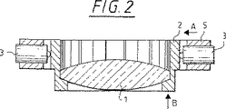
図2から明らかであるように、装着リング2は底部の開いた鉢形の形状を有し、2つの作動部材3はその上縁部に配置され、半径方向の力を発生させている。レンズ1は装着リング2の底部の楔形下縁部に当接し、作動部材3により図2の矢印Aの方向に力が加わったとき、レンズに対し、光軸と平行な矢印B方向の曲げモーメントが発生する。調整ねじとして構成されている作動部材3は油圧方式で作動されても良く、あるいは、必要に応じて別の方式で作動されても良い。図から明らかであるように、作動部材は、レンズ1のたわみという形の変形をもたらすモーメントを装着リング2に、各々の目的に応じて適切に導入する。
【0012】
図3及び図4はフレーム5を示し、このフレーム5においても、図1及び図2に示す実施形態の場合と同様に、変形自在の装着リング2にモーメントを導入する。特に図4から明らかであるように、この場合には、フレーム5と装着リング2は部分的に光軸と平行な方向で前後に位置しているので、この場合にも、互いに対向する2つの作動部材3の長手方向軸は光軸と平行であり、従って、同様に光軸と平行な向きの力を発生することができる。
【0013】
フレーム5を装着リング2と結合するために、作動部材3に対しそれぞれ90°ずれた位置に、固定部材又は締め付け部材4(詳細には図示せず)が設けられている。図1及び図2に示す実施形態とは異なり、装着リング2は2つの互いに真向かいの場所でフレーム5に固定保持され且つ90°ずれた位置では光軸に沿って曲げられる。
【0014】
図5及び図6に示す実施形態の場合、2つの互いに対向する位置では下方に向かって、また、それらの位置に対しそれぞれ90°ずれた位置では上方に向かって、対応して配置された作動部材3により押圧されるので、光軸に沿った摺動は起こらない。図から明らかなように、この場合、図3及び図4に示す実施形態と同様に、たとえば、水平に対向する作動部材は下向きの曲げモーメントを発生し、垂直に対向する作動部材3は上向きの曲げモーメントを発生して、それらのモーメントがレンズ1に作用する。装着リングとフレームとの結合は、作動部材3の相互間にそれぞれ周囲に対称に配分して配設される4つの連結体により行われる。
【0015】
図7は、圧電素子として構成されている原理上の作動部材3の断面図である。この場合、作動部材、すなわち、圧電素子3が圧電動作したとき、それらの素子の周囲に沿った配分状態に応じて所定の形態の曲げモーメントがレンズ1に加わるように、より多くの数、たとえば、20個の圧電素子をフレーム5又は装着リング2のリング部分に配分することができる。モーメントを導入するために、圧電素子4とレンズ1との間の中間部材として楔形のレンズ支え6がある。
【0016】
図8はもう一つの実施形態の一部断面図を示す。ここでも変形可能な装着リング2に保持されているレンズ1、ならびに装着リング2をかこむフレーム5が認められる。装着リング2の周縁フランジ10の厚さは外側円周で薄くなる。フレーム5の周縁フランジ11の内側円周は上記外側円周と同じ厚さで、そのため装着リング2とフレーム5の間で、リング状かつ溝状のくぼみを生じるようになっている。
【0017】
この溝状のくぼみにはリング状の作動部材ホルダ12が挿入され、図中番号13が示すように、フレーム5の周縁フランジ11にネジ止めされている。作動部材ホルダ12は、円周上複数の箇所に配置されてたとえば直径をはさむ2箇所で向かい合い、円筒形の取付口14を備えている。この取付口は、これよりも直径が小さい貫通孔15を経由して、作動部材ホルダ11の上側と連結している。このようにして取付口14と貫通口15の間に、リング状の肩16が生じる。
【0018】
いずれの取付口14にも空気圧ベローズ3があり、これはこの実施形態では作動部材として用いられている。このベローズ3の下側は、変形可能な装着リング2のリング状フランジ10に密着している。ベローズ3のリング状の上側前面は、取付口14と作動部材ホルダ11の貫通孔15の間の段状部分16に密着している。ベローズ3のかぎ形のソケット17は、貫通孔15を通ってホース18と連結し、加圧されたガスがこのホースから供給される。
【0019】
ガスの圧力調節はさまざまな方法で行うことができる:
【0020】
最も単純な場合では、調節弁(ここには図示せず)と装着リング2の両方またはそのいずれかに簡単なガス圧力センサを取り付け、このセンサがベローズ3で実際に得られているガス圧力に関する応答信号を制御装置に発する。別法として、装着リング2に光路センサ(ここには図示せず)を取りつけることができ、このセンサが装着リング2の実際の曲がりを検知し、それに応じて制御装置に通報する。この光路センサはたとえば静電容量の原理で動作させることができる。
【0021】
ガス圧力センサによるガス圧力調節も光路センサによる路程測定も、センサを複数備えることによってその精度を上げることができる。たとえば4つのガス圧力センサを備え、制御装置でそれらの信号を4つの較正済みのガス圧力曲線により修正することができる。これらガス圧力曲線は制御装置内に記憶されているもので、そのときどきのガス圧力に異常が生じていないかどうかの基準となるものである。同様に4つの光路センサを装着リング2に配設することもできる。
【0022】
装着リング2とフレーム5の連結は、ここでもまた一種の関節である装置で行われ、これらの装置はベローズ3間の角度範囲に備えられる。
【0023】
装着リング2とフレーム5の連結は、図9の実施形態で行うのがとくに優雅である。ここで装着リング2とフレーム5は1つの均質な加工物として製造され、図示された形態では複数のスリット20により機能上2つの部材2と5に区分されている。スリット20はたとえば放電加工によって設けることができる。これらのスリットはならんで、この光学系の軸を中心とするほぼ1つの円となり、隣り合う末端でわずかに半径方向外側に向きを変える。こうして装着リング2とフレーム5の間には、変形可能な関節として働く素材ブリッジ4が生じる。スリット20は、素材ブリッジ4に90°だけ位置をずらしたところに、半径方向に突出する舌状物21を形成する。これら舌状物にはそれぞれ今見ている図の平面の向こう側から、ベローズが1つずつ図8に示したと同様に作用する。このベローズはみずからの(今回はリング状ではない)作動部材ホルダによってポケット22(点線で示す)に収められ、このポケットは装着リング2とフレーム5の前面に設けられているが、その前面は今見ている図の平面の向こう側にあることになる。
【0024】
作動部材として空気圧で動作するベローズ3を使用することは、先に述べた実施形態とくらべてメカニズム上の原理が単純になるという利点がある。いかなる案内装置も不要であり、したがって摩擦と摩耗が大幅に解消する。また調節速度が速くなるのも利点である。
【0025】
作動部材3として多数の圧電素子を設けると共に、それらを周囲に沿って任意に配分することにより、任意の方向の非点収差、3波状態及び円筒レンズ効果のような他の効果を作り出すこと又は場合によっては重ね合わせることができる。 先に説明した作動部材の使用により、他のレンズの表面誤差の結像の誤りを補正することができるように、レンズ1をマウント部に対し変形させることが可能である。すなわち、1つ又はいくつかのレンズ1において「過補償」が行われることになる。この結果、対物レンズ全体の結像品質は改善される。さらに、石英のコンパクション又はレンズの温度上昇に起因する屈折の変化を稼動中に、対物レンズの寿命の全てを通して光学的品質が保証されるように補正することができる。
【0026】
一般に、レンズ1は対物レンズの上三分の一の部分で変形のために使用され、光束の光束直径とレンズ直径との比は、ゆがみ作用と非点収差作用との正しい関係を規定する。さらに、光束直径に沿った視野の推移を操作すべきである。絞り空間にあるレンズに関しては、視野全体にわたり一定である非点収差が起こり、ゆがみ作用は発生しない。レチクルに非常に近接しているレンズについては、ゆがみアナモルフィズムは起こるが、非点収差作用はごく小さい。
作動部材、特に圧電素子は減速又は加速のための直線伝動装置又はレバー伝動装置のような伝動装置を具備していても良い。この目的のために、固体連結体を使用できると有利である。
【図面の簡単な説明】
【図1】 本発明に従った作動部材を有する光学要素の概略平面図。
【図2】 図1の線II−IIに沿った断面図。
【図3】 本発明に従った作動部材を有する光学要素の第2の実施形態を示す図。
【図4】 図3の線IV−IVに沿った断面図。
【図5】 本発明に従った作動部材を有する光学要素の第3の実施形態を示す図。
【図6】 図5の線VI−VIに沿った断面図。
【図7】 作動部材の別の実施形態の図2,図4及び図6にならった断面図。
【図8】 本発明に従った作動部材を有する光学要素の第5の実施形態の部分断面図。
【図9】 図8に示した2部分構成の実施形態に代わる、装着リング及びそれと連結するフレームの一体型に実施形態の部分上面図。
【符号の説明】
1 レンズ
2 装着リング
3 作動部材
5 フレーム
6 レンズ支え[0001]
The invention has an optical element, in particular a lens or mirror, in particular having a slit-like field of view or illumination that is not rotationally symmetric and arranged on the mount, and an actuating member acting on part of the mount and / or the optical element In particular, the present invention relates to a projection exposure apparatus for microlithography.
[0002]
An optical system of the type mentioned at the outset is described in EP 0 678 768 A2. In this case, a step of transferring a narrow slit-shaped strip onto the wafer by a mask and a scanning process are applied. To expose the entire field of view, the reticle and wafer are slid sideways (scanning).
However, due to the slit-like shape, there is a drawback that copying of rotationally symmetric illumination occurs particularly with a lens close to the wafer. That is, as the lens temperature rises inevitably, a temperature distribution also occurs on the lens in a rotationally symmetric manner, and due to the linear relationship between the refractive index and temperature and thermal expansion, the image on the optical axis Deviation, for example, astigmatism, occurs.
[0003]
In 193 nm lithography, 193 nm light is transmitted through a quartz glass lens, thereby reducing the volume of quartz glass, and NI 2. Decreases monotonously according to Furthermore, an increase in refractive index occurs. N is the number of laser pulses and I is the pulse dose. An increase in refractive index overcompensates for a decrease in optical path due to contraction, so an effect called compaction interferes with the wavefront. As a result, an image shift such as astigmatism occurs on the optical axis as in the case of the temperature rise of the lens (lens heating).
[0004]
Contrary to compensation for lens temperature rise, there is no passive compensation for the compaction effect. In this case, changes in the wavefront would have to be actively compensated by changing the lens elements. Since there is no possibility of using active mirrors in refraction-based designs (the cost of introducing additional mirrors to compensate for imaging shifts is generally out of question), one or more lenses are used as “adjustment members” Must be used. In order to correct astigmatism on the optical axis, movement and decentration along the optical axis are out of the question. Therefore, there is no freedom of any translational movement as a possibility of correction.
In European Patent No. 0678768A, it is proposed to use a lens as an “adjusting member” in order to correct an image shift caused by an uneven temperature increase of the lens. According to FIG. 11, a force acting in the radial direction is applied to the lens. However, the force thus generated only causes an asymmetric thickness change.
EP 0660169 A1 describes a microlithographic projection exposure apparatus in which the objective lens comprises a correction element. For this purpose, in particular a pair of lenses is provided which are rotatable about the optical axis. The refractive index varies depending on the lens shape in which a cylindrical meniscus shape is superimposed on a spherical lens.
[0005]
It is an object of the present invention to provide an optical system of the type mentioned at the outset, which can correct or minimize image deviations inevitably caused by non-uniform temperature distribution in the optical system by simple means.
[0006]
The invention has an optical element, in particular a lens or mirror, in particular having a slit field of view or illumination that is not rotationally symmetric and arranged on the mount, and an actuating member acting on the optical element and / or the mount. An optical system, in particular a microlithographic projection exposure apparatus, in which the actuating member is not rotationally symmetric and deviates from the radial direction and / or in order to generate a bend that occurs with almost no change in thickness. A moment is generated with respect to the optical element.
[0007]
Unlike conventional techniques, rather than applying only a pressure that causes an asymmetric thickness change, a thrust or torsion is generated, so that an inevitable image shift is largely corrected. To cause bending of an optical element, for example, a lens. By using the actuating member according to the invention, the optical element, for example a lens, can be appropriately deformed from several hundred nm to μm. By this method, for example, astigmatism r 2 and r 4 can be compensated.
In the case of the method according to the invention, the desired temperature distribution can be achieved quickly and reliably using simple means. This is particularly important when a predetermined imaging deviation, such as a low-order imaging deviation, is to be corrected.
[0008]
Another very important advantage of the present invention is that "overcompensation" and additional correction of manufacturing errors are possible if necessary. Rather than symmetrizing individual lenses as seen in the prior art, “overcompensating” individual lenses, that is, deliberately making the temperature distribution or deformation asymmetrical in another direction You can also. In this way, when viewed as a whole, the entire objective lens or the exposure apparatus can be corrected.
[0009]
There are two variants of manufacturing error correction: simultaneous correction of accidental manufacturing error and deliberate incorporation of a fixed advance amount to halve the required correction amount.
According to the method of the present invention, it is possible to simultaneously compensate for the lens heating and the compaction effect of the optical element.
The optical system according to the invention is particularly advantageous when applied to semiconductor lithography. This is because, in the case of semiconductor lithography, the image shift that occurs as the reduction ratio of the structure to be imaged increases must be minimized.
With the actuating member of the present invention, thermal astigmatism and astigmatism for correcting errors based on the compaction effect of an optical element, for example, a lens can be generated according to the purpose.
Furthermore, depending on the arrangement and number of actuating members, it is advantageous that other variations of the optical element are possible.
Advantageous configurations of the invention will become apparent from the examples whose principles are illustrated on the basis of
[0010]
Since a projection exposure apparatus in microlithography is generally known, the following description will be limited to the optical element held by the
[0011]
As is apparent from FIG. 2, the
[0012]
3 and 4 show a
[0013]
In order to couple the
[0014]
In the case of the embodiments shown in FIGS. 5 and 6, correspondingly arranged operations are downwardly directed at two mutually opposite positions and upwardly at positions shifted by 90 ° with respect to those positions. Since it is pressed by the
[0015]
FIG. 7 is a sectional view of the operating
[0016]
FIG. 8 shows a partial cross-sectional view of another embodiment. Here again, the
[0017]
A ring-shaped
[0018]
Each mounting port 14 has a pneumatic bellows 3, which is used as an operating member in this embodiment. The lower side of the
[0019]
Gas pressure regulation can be done in various ways:
[0020]
In the simplest case, a simple gas pressure sensor is attached to the control valve (not shown here) and / or the mounting
[0021]
The accuracy of both the gas pressure adjustment by the gas pressure sensor and the path length measurement by the optical path sensor can be improved by providing a plurality of sensors. For example, four gas pressure sensors can be provided and their signals can be corrected by the controller with four calibrated gas pressure curves. These gas pressure curves are stored in the control device and serve as a reference for whether or not an abnormality has occurred in the gas pressure at that time. Similarly, four optical path sensors can be arranged on the mounting
[0022]
The connection of the mounting
[0023]
The connection of the mounting
[0024]
The use of the
[0025]
Providing a number of piezoelectric elements as actuating
[0026]
In general, the
The actuating member, in particular the piezoelectric element, may comprise a transmission such as a linear transmission or a lever transmission for deceleration or acceleration. For this purpose, it may be advantageous to use solid connections.
[Brief description of the drawings]
FIG. 1 is a schematic plan view of an optical element having an actuating member according to the present invention.
FIG. 2 is a cross-sectional view taken along line II-II in FIG.
FIG. 3 shows a second embodiment of an optical element having an actuating member according to the invention.
4 is a cross-sectional view taken along line IV-IV in FIG. 3;
FIG. 5 shows a third embodiment of an optical element having an actuating member according to the invention.
6 is a cross-sectional view taken along line VI-VI in FIG.
7 is a cross-sectional view according to FIGS. 2, 4 and 6 of another embodiment of an actuating member. FIG.
FIG. 8 is a partial cross-sectional view of a fifth embodiment of an optical element having an actuating member according to the present invention.
FIG. 9 is a partial top view of the embodiment of the mounting ring and the frame connecting to the mounting ring, in place of the two-part embodiment shown in FIG. 8;
[Explanation of symbols]
1
Claims (8)
作動部材(3)は、前記光軸を挟んで互いに対向する2つを対とした2対よりなり、第1の対の作動部材(3)は、厚さの変化を伴わずに起こる曲がりを発生させるために、光軸と平行な向きのスラスト及びモーメントのいずれか又は双方を光学要素(1)に発生させ、第2の対の作動部材(3)は、それらに対しそれぞれ90°位置のずれた前記スラスト又はモーメントと逆の向きのスラスト又はモーメントを発生させることを特徴とする光学系。 Lighting slit shaped field, or it will have an illumination is not rotationally symmetrical, is disposed on the mount portion, an optical element having an optical axis, an actuating member which acts on either or both of the optical element and the mount portion In an optical system having
The actuating member (3) is composed of two pairs of two facing each other across the optical axis, and the first pair of actuating members (3) is bent without any change in thickness. To generate, either or both thrust and moments oriented parallel to the optical axis are generated in the optical element (1), and the second pair of actuating members (3) are each at a 90 ° position relative to them. An optical system characterized by generating a thrust or moment in a direction opposite to the shifted thrust or moment .
Applications Claiming Priority (3)
| Application Number | Priority Date | Filing Date | Title |
|---|---|---|---|
| DE19827603A DE19827603A1 (en) | 1998-06-20 | 1998-06-20 | Projection light exposure system for microlithography |
| DE19827603.6 | 1998-06-20 | ||
| PCT/EP1999/004246 WO1999067683A2 (en) | 1998-06-20 | 1999-06-18 | Optical system, especially a projection light facility for microlithography |
Publications (2)
| Publication Number | Publication Date |
|---|---|
| JP2002519843A JP2002519843A (en) | 2002-07-02 |
| JP4357117B2 true JP4357117B2 (en) | 2009-11-04 |
Family
ID=7871556
Family Applications (1)
| Application Number | Title | Priority Date | Filing Date |
|---|---|---|---|
| JP2000556280A Expired - Fee Related JP4357117B2 (en) | 1998-06-20 | 1999-06-18 | Optical system, especially microlithographic projection exposure apparatus |
Country Status (7)
| Country | Link |
|---|---|
| US (1) | US6388823B1 (en) |
| EP (1) | EP1015931B1 (en) |
| JP (1) | JP4357117B2 (en) |
| KR (1) | KR100591306B1 (en) |
| DE (2) | DE19827603A1 (en) |
| TW (1) | TWI253509B (en) |
| WO (1) | WO1999067683A2 (en) |
Cited By (1)
| Publication number | Priority date | Publication date | Assignee | Title |
|---|---|---|---|---|
| US9579631B2 (en) | 2006-07-13 | 2017-02-28 | Sued-Chemie Ip Gmbh & Co. Kg | Process for the preparation of nanocrystalline metal oxides |
Families Citing this family (77)
| Publication number | Priority date | Publication date | Assignee | Title |
|---|---|---|---|---|
| DE19859634A1 (en) * | 1998-12-23 | 2000-06-29 | Zeiss Carl Fa | Optical system, in particular projection exposure system for microlithography |
| DE19908554A1 (en) * | 1999-02-27 | 2000-08-31 | Zeiss Carl Fa | Adjustable assembly |
| DE19956354B4 (en) | 1999-11-24 | 2004-02-19 | Carl Zeiss | Method to compensate for non-rotationally symmetrical imaging errors in an optical system |
| US6476986B2 (en) * | 1999-12-28 | 2002-11-05 | Texas Instruments Incorporated | Six-axis attachment apparatus and method for spatial light modulators |
| JP4809987B2 (en) | 2000-03-30 | 2011-11-09 | キヤノン株式会社 | Support structure for optical element, exposure apparatus using the same, and method for manufacturing semiconductor device |
| JP4945845B2 (en) | 2000-03-31 | 2012-06-06 | 株式会社ニコン | An optical element holding device, a lens barrel, an exposure apparatus, and a microdevice manufacturing method. |
| DE60132320T2 (en) | 2000-04-25 | 2008-05-08 | Asml Holding, N.V. | METHOD, SYSTEM AND DEVICE FOR PRECISELY POSITIONING AND ORIENTATION OF A LENS IN AN OPTICAL SYSTEM |
| US6574053B1 (en) | 2000-08-10 | 2003-06-03 | Nikon Corporation | Kinematic alignment structure for placement between components axially aligned in a cylindrical body |
| EP1312965B1 (en) * | 2000-08-18 | 2007-01-17 | Nikon Corporation | Optical element holding device |
| DE10046379A1 (en) * | 2000-09-20 | 2002-03-28 | Zeiss Carl | System for the targeted deformation of optical elements |
| EP1336206B1 (en) | 2000-11-21 | 2007-08-01 | Csir | Strain/electrical potential transducer |
| US6937394B2 (en) | 2001-04-10 | 2005-08-30 | Carl Zeiss Semiconductor Manufacturing Technologies Ag | Device and method for changing the stress-induced birefringence and/or the thickness of an optical component |
| DE10120446C2 (en) * | 2001-04-26 | 2003-04-17 | Zeiss Carl | Projection exposure system and method for compensating imaging errors in a projection exposure system, in particular for micro-lithography |
| DE10140608A1 (en) | 2001-08-18 | 2003-03-06 | Zeiss Carl | Device for adjusting an optical element |
| DE10151919B4 (en) * | 2001-10-20 | 2007-02-01 | Carl Zeiss Smt Ag | Exposure lens in semiconductor lithography |
| DE10220324A1 (en) | 2002-04-29 | 2003-11-13 | Zeiss Carl Smt Ag | Projection method with pupil filtering and projection lens for this |
| US20030234918A1 (en) * | 2002-06-20 | 2003-12-25 | Nikon Corporation | Adjustable soft mounts in kinematic lens mounting system |
| US6880942B2 (en) * | 2002-06-20 | 2005-04-19 | Nikon Corporation | Adaptive optic with discrete actuators for continuous deformation of a deformable mirror system |
| EP1576407A2 (en) | 2002-12-23 | 2005-09-21 | BAE Systems PLC | Deformable-mirror cooling |
| EP1576403A1 (en) * | 2002-12-23 | 2005-09-21 | BAE Systems PLC | Deformable-mirror holder |
| AU2003294125A1 (en) * | 2002-12-23 | 2004-07-14 | Bae Systems Plc | Deformable mirror |
| WO2004109357A1 (en) * | 2003-06-06 | 2004-12-16 | Nikon Corporation | Optical element holding device, lens barrel, exposing device, and device producing method |
| WO2005022614A1 (en) | 2003-08-28 | 2005-03-10 | Nikon Corporation | Exposure method and apparatus, and device manufacturing method |
| EP1695148B1 (en) * | 2003-11-24 | 2015-10-28 | Carl Zeiss SMT GmbH | Immersion objective |
| JP4654915B2 (en) | 2003-12-25 | 2011-03-23 | 株式会社ニコン | Optical element holding device, lens barrel, exposure apparatus, and device manufacturing method |
| KR101328356B1 (en) * | 2004-02-13 | 2013-11-11 | 가부시키가이샤 니콘 | Exposure method and system, and device production method |
| WO2005091077A2 (en) | 2004-02-20 | 2005-09-29 | Carl Zeiss Smt Ag | Projection lens of a microlithographic projection exposure system |
| DE102004035595B4 (en) | 2004-04-09 | 2008-02-07 | Carl Zeiss Smt Ag | Method for adjusting a projection objective |
| JP5629050B2 (en) * | 2004-06-10 | 2014-11-19 | カール・ツァイス・エスエムティー・ゲーエムベーハー | Projection objective for a microlithographic projection exposure apparatus |
| US7403264B2 (en) * | 2004-07-08 | 2008-07-22 | Asml Netherlands B.V. | Lithographic projection apparatus and a device manufacturing method using such lithographic projection apparatus |
| JP4843272B2 (en) * | 2004-07-31 | 2011-12-21 | カール・ツァイス・エスエムティー・ゲーエムベーハー | Optical system for microlithographic projection exposure apparatus |
| KR100687717B1 (en) * | 2004-12-16 | 2007-02-27 | 한국전자통신연구원 | Micro stage using PZT |
| US7436484B2 (en) * | 2004-12-28 | 2008-10-14 | Asml Netherlands B.V. | Lithographic apparatus and device manufacturing method |
| DE102005019726A1 (en) * | 2005-04-22 | 2006-10-26 | Carl Zeiss Smt Ag | Projection objective lens mounting and aligning method, for lithography, involves assembling optical units to form lens, which is mounted/aligned based on azimuth angular position, which is determined based on inhomogeneities of one unit |
| TWI454731B (en) * | 2005-05-27 | 2014-10-01 | Zeiss Carl Smt Gmbh | Method for improving the imaging properties of a projection objective, and such a projection objective |
| US20080204682A1 (en) * | 2005-06-28 | 2008-08-28 | Nikon Corporation | Exposure method and exposure apparatus, and device manufacturing method |
| DE102005031084A1 (en) * | 2005-06-28 | 2007-01-04 | Carl Zeiss Smt Ag | Microlithographic exposure method and projection exposure apparatus for carrying out the method |
| EP1746463A2 (en) | 2005-07-01 | 2007-01-24 | Carl Zeiss SMT AG | Method for correcting a lithographic projection objective and projection objective of such a kind |
| JP5069232B2 (en) | 2005-07-25 | 2012-11-07 | カール・ツァイス・エスエムティー・ゲーエムベーハー | Projection objective lens of microlithography projection exposure apparatus |
| WO2007087455A2 (en) * | 2006-01-30 | 2007-08-02 | Goodrich Corporation | Figuring of optical device for compensation of load-induced distortion |
| JP2007266511A (en) * | 2006-03-29 | 2007-10-11 | Nikon Corp | Optical system, exposure apparatus, and adjustment method of optical characteristic |
| DE102006016376B4 (en) * | 2006-04-05 | 2011-02-17 | Odelo Gmbh | Linsenverstellvorrichtung |
| DE102006034755A1 (en) * | 2006-07-24 | 2008-01-31 | Carl Zeiss Smt Ag | Optical device and method for correcting or improving the imaging behavior of an optical device |
| EP1882983A1 (en) * | 2006-07-25 | 2008-01-30 | Carl Zeiss SMT AG | Gravity compensating support for an optical element |
| DE102006047666A1 (en) * | 2006-09-28 | 2008-04-03 | Carl Zeiss Smt Ag | Projection lens for micro lithography, has multiple lenses with local optical axis, where one lens is assigned to manipulator with actuators, and input force or input torque is attained by former actuators |
| JP5242036B2 (en) * | 2006-10-12 | 2013-07-24 | 日立造船株式会社 | Laser processing equipment |
| KR101452534B1 (en) | 2007-01-22 | 2014-10-21 | 칼 짜이스 에스엠티 게엠베하 | Method for improving imaging properties of an optical system, and optical system |
| DE102008006687A1 (en) | 2007-01-22 | 2008-07-24 | Carl Zeiss Smt Ag | Optical system's image characteristics improving method for use as projection objective, involves deforming optical elements by mechanical force effect from mechanical manipulators and thermal effect from thermal manipulators, respectively |
| DE102007010906A1 (en) * | 2007-03-05 | 2008-09-11 | Seereal Technologies S.A. | Imaging device for influencing incident light |
| DE102008016011A1 (en) | 2007-03-27 | 2008-10-02 | Carl Zeiss Smt Ag | Correction of optical elements by means of flatly irradiated correction light |
| DE102008041287A1 (en) | 2007-08-24 | 2009-02-26 | Carl Zeiss Smt Ag | Actuator arrangement for deforming e.g. lens, of optical arrangement of microlithography device, has actuator devices exerting actuator forces on body until reaching maximum force values, where one value is smaller than other value |
| WO2009110963A2 (en) * | 2008-02-29 | 2009-09-11 | Corning Incorporated | Kinematic optical mount |
| JP2010021535A (en) | 2008-06-11 | 2010-01-28 | Canon Inc | Deforming mechanism, exposure equipment, and method for manufacturing device |
| DE102008049616B4 (en) | 2008-09-30 | 2012-03-29 | Carl Zeiss Smt Gmbh | Projection exposure apparatus for microlithography for the production of semiconductor devices |
| US7916408B2 (en) | 2008-10-30 | 2011-03-29 | Corning Incorporated | X-Y adjustable optical mount |
| DE102008063223B3 (en) * | 2008-12-23 | 2010-09-09 | Jenoptik Laser, Optik, Systeme Gmbh | Monolithic optical socket |
| DE102009005954B4 (en) * | 2009-01-20 | 2010-10-21 | Carl Zeiss Smt Ag | damping device |
| DE102009054868A1 (en) | 2009-02-06 | 2010-08-12 | Carl Zeiss Smt Ag | Control pressure adjusting method for pneumatically operatable bellow that is utilized for e.g. positioning lens for manipulator of projection system, involves transmitting working pressure for actuator elements in to control pressure |
| JP5511199B2 (en) | 2009-02-25 | 2014-06-04 | キヤノン株式会社 | Projection optical system, exposure apparatus, and device manufacturing method |
| WO2010098474A1 (en) * | 2009-02-27 | 2010-09-02 | 株式会社 ニコン | Optical element holding device, optical system, exposure apapratus, device manufacturing method, and interchange method for optical element |
| JP2010219080A (en) * | 2009-03-13 | 2010-09-30 | Canon Inc | Optical device, stage device, optical system, and exposure apparatus |
| JP2010217280A (en) * | 2009-03-13 | 2010-09-30 | Ricoh Co Ltd | Imaging lens, image reading device using the same, and image forming apparatus |
| DE102009037135B4 (en) * | 2009-07-31 | 2013-07-04 | Carl Zeiss Laser Optics Gmbh | Holding device for an optical element |
| CN101644880B (en) * | 2009-09-09 | 2011-04-27 | 中国科学技术大学 | Laser light projection display system and method thereof |
| WO2011116792A1 (en) | 2010-03-26 | 2011-09-29 | Carl Zeiss Smt Gmbh | Optical system, exposure apparatus, and waverfront correction method |
| JP5904749B2 (en) * | 2011-10-14 | 2016-04-20 | キヤノン株式会社 | Optical element holding device, lens device having the same, and imaging device |
| CN105283789A (en) * | 2013-02-13 | 2016-01-27 | 齐戈股份有限公司 | Monolithic optical components with integrated flexures |
| DE102013110750B3 (en) | 2013-09-27 | 2014-11-13 | Jenoptik Optical Systems Gmbh | Optical assembly with a socket with thermally dependent force compensation |
| JP5686171B2 (en) * | 2013-10-15 | 2015-03-18 | 株式会社リコー | Imaging lens, image reading apparatus and image forming apparatus using the same |
| DE102015101384B3 (en) * | 2015-01-30 | 2015-11-12 | Jenoptik Optical Systems Gmbh | Optical socket with at least one clamping unit with a pressure screw |
| DE102015101385B3 (en) * | 2015-01-30 | 2016-01-21 | Jenoptik Optical Systems Gmbh | Optical socket with at least one clamping unit with a lag screw |
| US10095089B2 (en) * | 2016-05-17 | 2018-10-09 | Raytheon Company | Lens mount assembly |
| DE102017117468B3 (en) | 2017-08-02 | 2018-09-20 | Jenoptik Optical Systems Gmbh | Device for variably influencing the wavefront of a beam with a plano-optic deformable over its peripheral surface |
| CN109856923B (en) * | 2017-11-30 | 2021-03-09 | 上海微电子装备(集团)股份有限公司 | Image quality compensation device and method and optical system |
| CN111381359B (en) * | 2018-12-27 | 2021-04-30 | 上海微电子装备(集团)股份有限公司 | Image quality compensation device, optical system and photoetching machine |
| DE102019200981B3 (en) | 2019-01-25 | 2020-06-25 | Carl Zeiss Smt Gmbh | Projection exposure system for microlithography |
| DE102019201147A1 (en) | 2019-01-30 | 2020-07-30 | Carl Zeiss Smt Gmbh | Projection exposure system for semiconductor lithography with an optical arrangement |
Family Cites Families (23)
| Publication number | Priority date | Publication date | Assignee | Title |
|---|---|---|---|---|
| US4155631A (en) | 1977-04-14 | 1979-05-22 | W. J. Schafer Associates, Inc. | Apparatus for compensating for thermally introduced distortions in reflecting surfaces |
| US4226507A (en) * | 1979-07-09 | 1980-10-07 | The Perkin-Elmer Corporation | Three actuator deformable specimen |
| US4492431A (en) * | 1982-05-04 | 1985-01-08 | United Technologies Corporation | Pressure actuated deformable mirror |
| JPS59144127A (en) | 1983-02-07 | 1984-08-18 | Canon Inc | Optical apparatus with adjustment of image |
| JPS61165837A (en) * | 1985-01-16 | 1986-07-26 | Matsushita Electric Ind Co Ltd | Laser light emitter |
| JPS6232613A (en) * | 1985-08-05 | 1987-02-12 | Canon Inc | Projection exposure device |
| US4647164A (en) * | 1985-11-21 | 1987-03-03 | The United States Of America As Represented By The United States Department Of Energy | Apparatus for and method of correcting for astigmatism in a light beam reflected off of a light reflecting surface |
| US4993823A (en) | 1989-06-29 | 1991-02-19 | Eastman Kodak Company | Method for correction of distortions of an imaging device |
| US5053794A (en) * | 1989-12-08 | 1991-10-01 | Benz William G | Universal adapter for attaching a camera to associated optical devices such as telescopes, microscopes and the like |
| US5457577A (en) * | 1992-01-22 | 1995-10-10 | The United States Of America As Represented By The Secretary Of The Army | Quick-set precision optical holder |
| JP3259373B2 (en) * | 1992-11-27 | 2002-02-25 | 株式会社日立製作所 | Exposure method and exposure apparatus |
| JP3341269B2 (en) | 1993-12-22 | 2002-11-05 | 株式会社ニコン | Projection exposure apparatus, exposure method, semiconductor manufacturing method, and projection optical system adjustment method |
| JP3368091B2 (en) * | 1994-04-22 | 2003-01-20 | キヤノン株式会社 | Projection exposure apparatus and device manufacturing method |
| US5557469A (en) | 1994-10-28 | 1996-09-17 | Ultratech Stepper, Inc. | Beamsplitter in single fold optical system and optical variable magnification method and system |
| JP3894509B2 (en) | 1995-08-07 | 2007-03-22 | キヤノン株式会社 | Optical apparatus, exposure apparatus, and device manufacturing method |
| JPH1039208A (en) * | 1996-07-23 | 1998-02-13 | Nikon Corp | Projection optical system |
| JPH1054932A (en) * | 1996-08-08 | 1998-02-24 | Nikon Corp | Projection optical device and projection exposure device provided the device |
| JPH10144602A (en) * | 1996-11-14 | 1998-05-29 | Nikon Corp | Reflecfing mirror holder and projection aligner |
| JPH10206714A (en) * | 1997-01-20 | 1998-08-07 | Canon Inc | Lens moving device |
| US5923482A (en) * | 1997-03-14 | 1999-07-13 | Waters Investments Limited | Changing astigmatism in an optical system |
| JP3445105B2 (en) * | 1997-07-25 | 2003-09-08 | キヤノン株式会社 | Optical element moving device |
| JP4043560B2 (en) * | 1997-09-25 | 2008-02-06 | フジノン株式会社 | Optical lens |
| US5986827A (en) * | 1998-06-17 | 1999-11-16 | The Regents Of The University Of California | Precision tip-tilt-piston actuator that provides exact constraint |
-
1998
- 1998-06-20 DE DE19827603A patent/DE19827603A1/en not_active Withdrawn
-
1999
- 1999-05-28 KR KR1019990019501A patent/KR100591306B1/en not_active IP Right Cessation
- 1999-06-17 TW TW088110136A patent/TWI253509B/en not_active IP Right Cessation
- 1999-06-18 EP EP99929277A patent/EP1015931B1/en not_active Expired - Lifetime
- 1999-06-18 US US09/486,017 patent/US6388823B1/en not_active Expired - Lifetime
- 1999-06-18 DE DE59913282T patent/DE59913282D1/en not_active Expired - Lifetime
- 1999-06-18 WO PCT/EP1999/004246 patent/WO1999067683A2/en active IP Right Grant
- 1999-06-18 JP JP2000556280A patent/JP4357117B2/en not_active Expired - Fee Related
Cited By (1)
| Publication number | Priority date | Publication date | Assignee | Title |
|---|---|---|---|---|
| US9579631B2 (en) | 2006-07-13 | 2017-02-28 | Sued-Chemie Ip Gmbh & Co. Kg | Process for the preparation of nanocrystalline metal oxides |
Also Published As
| Publication number | Publication date |
|---|---|
| DE19827603A1 (en) | 1999-12-23 |
| WO1999067683A3 (en) | 2000-04-20 |
| DE59913282D1 (en) | 2006-05-18 |
| US6388823B1 (en) | 2002-05-14 |
| EP1015931B1 (en) | 2006-03-29 |
| JP2002519843A (en) | 2002-07-02 |
| WO1999067683A8 (en) | 2000-05-25 |
| WO1999067683A2 (en) | 1999-12-29 |
| EP1015931A2 (en) | 2000-07-05 |
| KR100591306B1 (en) | 2006-06-19 |
| KR20000005738A (en) | 2000-01-25 |
| TWI253509B (en) | 2006-04-21 |
Similar Documents
| Publication | Publication Date | Title |
|---|---|---|
| JP4357117B2 (en) | Optical system, especially microlithographic projection exposure apparatus | |
| KR100596062B1 (en) | Catadioptric projection objective with adaptive mirror and projection exposure method | |
| US7294814B2 (en) | Microlithography projection objective including deformable mirror with adjusting elements and systems and methods using the same | |
| JP4945845B2 (en) | An optical element holding device, a lens barrel, an exposure apparatus, and a microdevice manufacturing method. | |
| US20160209752A1 (en) | Optical device having a deformable optical element | |
| US7656595B2 (en) | Adjustment arrangement of an optical element | |
| TWI424186B (en) | Objective, in particular projection objective for semiconductor lithography | |
| JP4565261B2 (en) | Optical element holding mechanism, optical system barrel, and exposure apparatus | |
| US6398373B1 (en) | Pneumatic control system and method for shaping deformable mirrors in lithographic projection systems | |
| KR100368192B1 (en) | Projection type exposure apparatus | |
| KR20020022594A (en) | Optical element deformation system | |
| KR19980064731A (en) | Projection exposure apparatus and device manufacturing method | |
| JP2006113414A (en) | Optical element holding apparatus, lens barrel, exposure apparatus, and method for manufacturing micro device | |
| KR101122881B1 (en) | Projection lens of a microlithographic projection exposure system | |
| KR101490191B1 (en) | Optical element module with minimized parasitic loads | |
| WO2007071353A1 (en) | Imaging device in a projection exposure machine | |
| US7859643B2 (en) | Apparatus for moving curved-surface mirror, exposure apparatus and device manufacturing method | |
| JP3631045B2 (en) | DRIVE DEVICE, OPTICAL ELEMENT DRIVE DEVICE, EXPOSURE DEVICE, AND DEVICE MANUFACTURING METHOD | |
| WO2008122313A1 (en) | Optical element module with imaging error and position correction | |
| KR100486871B1 (en) | Projection exposure equipment | |
| JP4929529B2 (en) | OPTICAL SYSTEM MANUFACTURING METHOD AND EXPOSURE APPARATUS PROVIDED WITH OPTICAL SYSTEM PRODUCED BY THE MANUFACTURING METHOD | |
| CN109416515B (en) | Holding device, projection optical system, exposure device, and article manufacturing method | |
| WO2009124590A1 (en) | Optical aperture device | |
| EP2697688B1 (en) | Facet mirror device | |
| US5930324A (en) | Exposure apparatus and device manufacturing method using the same |
Legal Events
| Date | Code | Title | Description |
|---|---|---|---|
| A711 | Notification of change in applicant |
Free format text: JAPANESE INTERMEDIATE CODE: A711 Effective date: 20040802 |
|
| A521 | Written amendment |
Free format text: JAPANESE INTERMEDIATE CODE: A821 Effective date: 20040802 |
|
| A621 | Written request for application examination |
Free format text: JAPANESE INTERMEDIATE CODE: A621 Effective date: 20060602 |
|
| RD03 | Notification of appointment of power of attorney |
Free format text: JAPANESE INTERMEDIATE CODE: A7423 Effective date: 20080717 |
|
| RD04 | Notification of resignation of power of attorney |
Free format text: JAPANESE INTERMEDIATE CODE: A7424 Effective date: 20080919 |
|
| A131 | Notification of reasons for refusal |
Free format text: JAPANESE INTERMEDIATE CODE: A131 Effective date: 20090331 |
|
| A521 | Written amendment |
Free format text: JAPANESE INTERMEDIATE CODE: A523 Effective date: 20090615 |
|
| TRDD | Decision of grant or rejection written | ||
| A01 | Written decision to grant a patent or to grant a registration (utility model) |
Free format text: JAPANESE INTERMEDIATE CODE: A01 Effective date: 20090707 |
|
| A01 | Written decision to grant a patent or to grant a registration (utility model) |
Free format text: JAPANESE INTERMEDIATE CODE: A01 |
|
| A61 | First payment of annual fees (during grant procedure) |
Free format text: JAPANESE INTERMEDIATE CODE: A61 Effective date: 20090804 |
|
| FPAY | Renewal fee payment (event date is renewal date of database) |
Free format text: PAYMENT UNTIL: 20120814 Year of fee payment: 3 |
|
| R150 | Certificate of patent or registration of utility model |
Free format text: JAPANESE INTERMEDIATE CODE: R150 |
|
| FPAY | Renewal fee payment (event date is renewal date of database) |
Free format text: PAYMENT UNTIL: 20120814 Year of fee payment: 3 |
|
| FPAY | Renewal fee payment (event date is renewal date of database) |
Free format text: PAYMENT UNTIL: 20130814 Year of fee payment: 4 |
|
| R250 | Receipt of annual fees |
Free format text: JAPANESE INTERMEDIATE CODE: R250 |
|
| R250 | Receipt of annual fees |
Free format text: JAPANESE INTERMEDIATE CODE: R250 |
|
| R250 | Receipt of annual fees |
Free format text: JAPANESE INTERMEDIATE CODE: R250 |
|
| LAPS | Cancellation because of no payment of annual fees |