JP4345357B2 - Manufacturing method of semiconductor wafer - Google Patents
Manufacturing method of semiconductor wafer Download PDFInfo
- Publication number
- JP4345357B2 JP4345357B2 JP2003149782A JP2003149782A JP4345357B2 JP 4345357 B2 JP4345357 B2 JP 4345357B2 JP 2003149782 A JP2003149782 A JP 2003149782A JP 2003149782 A JP2003149782 A JP 2003149782A JP 4345357 B2 JP4345357 B2 JP 4345357B2
- Authority
- JP
- Japan
- Prior art keywords
- semiconductor wafer
- grinding
- double
- manufacturing
- semi
- Prior art date
- Legal status (The legal status is an assumption and is not a legal conclusion. Google has not performed a legal analysis and makes no representation as to the accuracy of the status listed.)
- Expired - Fee Related
Links
- 239000004065 semiconductor Substances 0.000 title claims description 34
- 238000004519 manufacturing process Methods 0.000 title claims description 31
- 238000000034 method Methods 0.000 claims description 59
- 238000005498 polishing Methods 0.000 claims description 27
- 239000006061 abrasive grain Substances 0.000 claims description 26
- 238000005530 etching Methods 0.000 claims description 7
- 238000007517 polishing process Methods 0.000 claims description 5
- 235000012431 wafers Nutrition 0.000 description 49
- 239000002002 slurry Substances 0.000 description 14
- 239000011148 porous material Substances 0.000 description 8
- 238000010586 diagram Methods 0.000 description 6
- 235000013339 cereals Nutrition 0.000 description 5
- 239000000463 material Substances 0.000 description 4
- 229920002635 polyurethane Polymers 0.000 description 4
- 239000004814 polyurethane Substances 0.000 description 4
- 239000013078 crystal Substances 0.000 description 3
- 230000000694 effects Effects 0.000 description 3
- 238000003754 machining Methods 0.000 description 3
- 238000007796 conventional method Methods 0.000 description 2
- 238000005187 foaming Methods 0.000 description 2
- 239000002245 particle Substances 0.000 description 2
- 238000003672 processing method Methods 0.000 description 2
- 230000002393 scratching effect Effects 0.000 description 2
- 240000007594 Oryza sativa Species 0.000 description 1
- 235000007164 Oryza sativa Nutrition 0.000 description 1
- 238000005336 cracking Methods 0.000 description 1
- 239000002440 industrial waste Substances 0.000 description 1
- 239000002184 metal Substances 0.000 description 1
- 239000000843 powder Substances 0.000 description 1
- 235000009566 rice Nutrition 0.000 description 1
- 238000005096 rolling process Methods 0.000 description 1
- 230000003746 surface roughness Effects 0.000 description 1
- 239000002699 waste material Substances 0.000 description 1
Images


Classifications
-
- H—ELECTRICITY
- H01—ELECTRIC ELEMENTS
- H01L—SEMICONDUCTOR DEVICES NOT COVERED BY CLASS H10
- H01L21/00—Processes or apparatus adapted for the manufacture or treatment of semiconductor or solid state devices or of parts thereof
- H01L21/02—Manufacture or treatment of semiconductor devices or of parts thereof
- H01L21/04—Manufacture or treatment of semiconductor devices or of parts thereof the devices having potential barriers, e.g. a PN junction, depletion layer or carrier concentration layer
- H01L21/18—Manufacture or treatment of semiconductor devices or of parts thereof the devices having potential barriers, e.g. a PN junction, depletion layer or carrier concentration layer the devices having semiconductor bodies comprising elements of Group IV of the Periodic Table or AIIIBV compounds with or without impurities, e.g. doping materials
- H01L21/30—Treatment of semiconductor bodies using processes or apparatus not provided for in groups H01L21/20 - H01L21/26
- H01L21/302—Treatment of semiconductor bodies using processes or apparatus not provided for in groups H01L21/20 - H01L21/26 to change their surface-physical characteristics or shape, e.g. etching, polishing, cutting
- H01L21/304—Mechanical treatment, e.g. grinding, polishing, cutting
-
- H—ELECTRICITY
- H01—ELECTRIC ELEMENTS
- H01L—SEMICONDUCTOR DEVICES NOT COVERED BY CLASS H10
- H01L21/00—Processes or apparatus adapted for the manufacture or treatment of semiconductor or solid state devices or of parts thereof
- H01L21/02—Manufacture or treatment of semiconductor devices or of parts thereof
- H01L21/02002—Preparing wafers
- H01L21/02005—Preparing bulk and homogeneous wafers
- H01L21/02008—Multistep processes
- H01L21/0201—Specific process step
- H01L21/02013—Grinding, lapping
-
- B—PERFORMING OPERATIONS; TRANSPORTING
- B24—GRINDING; POLISHING
- B24B—MACHINES, DEVICES, OR PROCESSES FOR GRINDING OR POLISHING; DRESSING OR CONDITIONING OF ABRADING SURFACES; FEEDING OF GRINDING, POLISHING, OR LAPPING AGENTS
- B24B37/00—Lapping machines or devices; Accessories
- B24B37/04—Lapping machines or devices; Accessories designed for working plane surfaces
- B24B37/042—Lapping machines or devices; Accessories designed for working plane surfaces operating processes therefor
-
- B—PERFORMING OPERATIONS; TRANSPORTING
- B24—GRINDING; POLISHING
- B24B—MACHINES, DEVICES, OR PROCESSES FOR GRINDING OR POLISHING; DRESSING OR CONDITIONING OF ABRADING SURFACES; FEEDING OF GRINDING, POLISHING, OR LAPPING AGENTS
- B24B37/00—Lapping machines or devices; Accessories
- B24B37/04—Lapping machines or devices; Accessories designed for working plane surfaces
- B24B37/07—Lapping machines or devices; Accessories designed for working plane surfaces characterised by the movement of the work or lapping tool
- B24B37/08—Lapping machines or devices; Accessories designed for working plane surfaces characterised by the movement of the work or lapping tool for double side lapping
-
- B—PERFORMING OPERATIONS; TRANSPORTING
- B24—GRINDING; POLISHING
- B24B—MACHINES, DEVICES, OR PROCESSES FOR GRINDING OR POLISHING; DRESSING OR CONDITIONING OF ABRADING SURFACES; FEEDING OF GRINDING, POLISHING, OR LAPPING AGENTS
- B24B37/00—Lapping machines or devices; Accessories
- B24B37/11—Lapping tools
- B24B37/20—Lapping pads for working plane surfaces
- B24B37/24—Lapping pads for working plane surfaces characterised by the composition or properties of the pad materials
- B24B37/245—Pads with fixed abrasives
-
- B—PERFORMING OPERATIONS; TRANSPORTING
- B24—GRINDING; POLISHING
- B24B—MACHINES, DEVICES, OR PROCESSES FOR GRINDING OR POLISHING; DRESSING OR CONDITIONING OF ABRADING SURFACES; FEEDING OF GRINDING, POLISHING, OR LAPPING AGENTS
- B24B7/00—Machines or devices designed for grinding plane surfaces on work, including polishing plane glass surfaces; Accessories therefor
- B24B7/10—Single-purpose machines or devices
- B24B7/16—Single-purpose machines or devices for grinding end-faces, e.g. of gauges, rollers, nuts, piston rings
- B24B7/17—Single-purpose machines or devices for grinding end-faces, e.g. of gauges, rollers, nuts, piston rings for simultaneously grinding opposite and parallel end faces, e.g. double disc grinders
-
- B—PERFORMING OPERATIONS; TRANSPORTING
- B24—GRINDING; POLISHING
- B24B—MACHINES, DEVICES, OR PROCESSES FOR GRINDING OR POLISHING; DRESSING OR CONDITIONING OF ABRADING SURFACES; FEEDING OF GRINDING, POLISHING, OR LAPPING AGENTS
- B24B9/00—Machines or devices designed for grinding edges or bevels on work or for removing burrs; Accessories therefor
- B24B9/02—Machines or devices designed for grinding edges or bevels on work or for removing burrs; Accessories therefor characterised by a special design with respect to properties of materials specific to articles to be ground
- B24B9/06—Machines or devices designed for grinding edges or bevels on work or for removing burrs; Accessories therefor characterised by a special design with respect to properties of materials specific to articles to be ground of non-metallic inorganic material, e.g. stone, ceramics, porcelain
- B24B9/065—Machines or devices designed for grinding edges or bevels on work or for removing burrs; Accessories therefor characterised by a special design with respect to properties of materials specific to articles to be ground of non-metallic inorganic material, e.g. stone, ceramics, porcelain of thin, brittle parts, e.g. semiconductors, wafers
-
- H—ELECTRICITY
- H01—ELECTRIC ELEMENTS
- H01L—SEMICONDUCTOR DEVICES NOT COVERED BY CLASS H10
- H01L21/00—Processes or apparatus adapted for the manufacture or treatment of semiconductor or solid state devices or of parts thereof
- H01L21/02—Manufacture or treatment of semiconductor devices or of parts thereof
- H01L21/02002—Preparing wafers
- H01L21/02005—Preparing bulk and homogeneous wafers
- H01L21/02008—Multistep processes
-
- H—ELECTRICITY
- H01—ELECTRIC ELEMENTS
- H01L—SEMICONDUCTOR DEVICES NOT COVERED BY CLASS H10
- H01L21/00—Processes or apparatus adapted for the manufacture or treatment of semiconductor or solid state devices or of parts thereof
- H01L21/02—Manufacture or treatment of semiconductor devices or of parts thereof
- H01L21/04—Manufacture or treatment of semiconductor devices or of parts thereof the devices having potential barriers, e.g. a PN junction, depletion layer or carrier concentration layer
- H01L21/18—Manufacture or treatment of semiconductor devices or of parts thereof the devices having potential barriers, e.g. a PN junction, depletion layer or carrier concentration layer the devices having semiconductor bodies comprising elements of Group IV of the Periodic Table or AIIIBV compounds with or without impurities, e.g. doping materials
- H01L21/30—Treatment of semiconductor bodies using processes or apparatus not provided for in groups H01L21/20 - H01L21/26
- H01L21/302—Treatment of semiconductor bodies using processes or apparatus not provided for in groups H01L21/20 - H01L21/26 to change their surface-physical characteristics or shape, e.g. etching, polishing, cutting
- H01L21/306—Chemical or electrical treatment, e.g. electrolytic etching
- H01L21/30625—With simultaneous mechanical treatment, e.g. mechanico-chemical polishing
Landscapes
- Engineering & Computer Science (AREA)
- Mechanical Engineering (AREA)
- Microelectronics & Electronic Packaging (AREA)
- General Physics & Mathematics (AREA)
- Manufacturing & Machinery (AREA)
- Computer Hardware Design (AREA)
- Physics & Mathematics (AREA)
- Power Engineering (AREA)
- Condensed Matter Physics & Semiconductors (AREA)
- Chemical & Material Sciences (AREA)
- Ceramic Engineering (AREA)
- Inorganic Chemistry (AREA)
- Mechanical Treatment Of Semiconductor (AREA)
- Finish Polishing, Edge Sharpening, And Grinding By Specific Grinding Devices (AREA)
- Polishing Bodies And Polishing Tools (AREA)
Description
【0001】
【発明の属する技術分野】
本発明は、単結晶インゴットから高平坦度、低加工歪みの半導体ウェーハを得る方法に係り、より詳しくは、遊離砥粒を用いた半固定砥粒研削により、半導体ウェーハを平坦化しつつ、ワイヤーソースライスまたは両頭研削で発生する微小な表面うねりを低減するとともに、従来の半導体ウェーハ製造プロセスを簡略化するための半導体ウェーハ製造方法に関する。
【0002】
【従来の技術】
一般に、半導体ウェーハの製造方法には、1)単結晶引上装置によって引き上げられた単結晶インゴットをスライスして薄円盤状のウェーハを得るスライス工程、2)ウェーハの欠けやワレを防ぐための面取工程、3)面取りされたウェーハを平坦化するためのラッピング工程、4)前記加工によりウェーハに発生した加工歪み層を除去するためのエッチング工程、5)面取り部を仕上げ研磨する面取り研磨工程、6)前記ウェーハを片面あるいは両面を研磨する研磨工程、7)前記ウェーハの仕上げ研磨を行う工程が採用されている。
【0003】
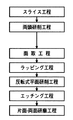
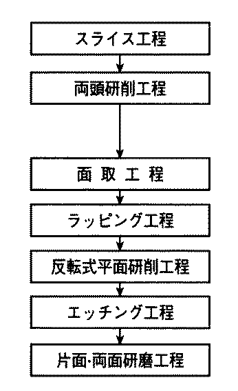
そして、上記のような一般的な半導体ウェーハの製造方法における平坦度の向上と微小な表面うねりの低減を目的として、図6に示すように、スライス工程、面取工程、ラッピング工程後に、両面の反転式平面研削工程を行い、必要に応じて残留歪み除去のエッチング工程を行い、両面研磨工程で仕上げる方法(特許文献1参照)や、図7に示すように、スライス工程後に、両頭研削工程を行い、面取工程、ラッピング工程後に、両面の反転式平面研削工程を行い、必要に応じて残留歪み除去のエッチング工程を行い、片面または両面研磨工程で仕上げる方法(特許文献2の段落【0002】参照)等が提案されている。
【0004】
しかるに、前記した従来の半導体ウェーハの製造方法におけるラッピング工程で用いられるラッピング装置は、ウェーハの大口径化に伴い大型化し、消耗資材や装置コストの上昇、ウェーハの大口径化および装置の巨大化に伴う作業者の作業負荷の増大、使用資材増加による産業廃棄物(廃研磨粉)の増加等の各課題が顕著化している。また、片面研削をスライス直後に行った場合、ワイヤーソーで生じたうねりを除去できないという問題がある。この問題を解決する手段として、ラッピング装置を両頭研削盤に置き換えて製造する方法が、種々提案されているが、両頭研削盤で製造されたウェーハの表面には、両頭研削加工に起因する微小表面うねり(高低差数+μm、周期数mm)が生じる問題がある。そこで、微小表面うねりを低減し、より均一な表面を得るために、両頭研削後に弾性体定盤を用いたラッピング加工を行い製造工程を簡略化する方法が提案されている(特許文献2に記載の発明)。しかしながら、この方法は、金属定盤に比較して砥粒がソフトに作用し加工歪みの少ないウェーハ表面が得られるが、加工速度が低く、また、弾性体定盤が著しく磨耗してウェーハの平坦度精度を維持できないという問題がある。
【0005】
【特許文献1】
特開平9−246216号公報
【特許文献2】
特開2002−124490号公報
【0006】
【発明が解決しようとする課題】
本発明は、上記した従来技術の問題を解決するためになされたもので、遊離砥粒を用いた半固定砥粒研削により、ワイヤーソースライスまたは両頭研削で発生する微小な表面うねりを低減するとともに、従来の半導体ウェーハ製造プロセスを簡略化し得る半導体ウェーハ製造方法の提供を目的とするものである。
【0007】
【課題を解決するための手段】
本発明に係る半導体ウェーハの製造方法は、スライス工程後に、面取工程、エッチング工程、片面または両面研磨工程の各工程を行う半導体ウェーハの製造方法であって、前記スライス工程後かつ前記面取工程前に、多孔質状の研磨パッドの表面孔に遊離砥粒を保持し、該研磨パッドの表面と半導体ウェーハ表面とを接触させた状態で該半導体ウェーハ表面を研削する半固定砥粒研削工程を行うことを特徴とする。更には、スライス工程後かつ半固定砥粒研削工程前に、半導体ウェーハの表裏両面を上下の砥石により同時に研削する両頭研削工程を行うことを特徴とする。
【0008】
本発明における多孔質状の研磨パッドと遊離砥粒を用いた半固定砥粒研削工程とは、例えば多孔質状のポリウレタンパッドに番手#400〜#1000程度の遊離砥粒を低濃度で供給することで、砥粒が研磨パッド表面の孔に保持されて半固定砥粒状態でウエーハを研削する方法をいう。この方法によれば、パッド表面に半固定状態で保持された砥粒による引っ掻き作用によりウエーハが研削されるので、スライス等の前工程で発生した微小うねりを低減することが可能となる。
【0009】
通常、ラッピングとは砥粒濃度20wt%程度のスラリーを定盤に供給し、ウェーハと定盤間のスラリ一層中にある砥粒の転動によってウェーハ表面に発生した脆性破壊作用を原理とした加工方法である。それに対し、本発明における半固定砥粒研削は、スラリー中の砥粒濃度を従来の約1/10程度に低下させることによりスラリー層を薄くし、砥粒を多孔質状のパッド表面の孔(ボア)に保持させることで砥粒の引っ掻き作用を生じさせる加工原理に基づくものである。
【0010】
従って、本発明方法によれば、高能率で比較的加工歪みの少ない良好な仕上げ面が得られ、スライス工程または両頭研削工程で生じた表面の微小うねりを除去できる。また、砥粒濃度を従来の約1/10程度に低下させて使用するために砥粒の使用量が少なく、消耗資材の削減による低コストを実現することができる上、スラリー中の砥粒濃度を低濃度にすることで、研磨パッドが著しく摩耗することがなく、ウェーハの平坦度精度を維持できる。さらに、本発明は、上記半固定砥粒研削工程をスライス工程後、またはスライス工程、両頭研削工程後に行うことにより、従来のラッピング工程、反転式平面研削工程を省略することができ、製造工程を簡略化できる。
【0011】
なお、本発明の半固定砥粒研削工程で用いる研削手段としては、一度に複数のウエーハを加工するバッチ式の両面研磨機またはラッピング装置等の既存の装置に多孔質状のパッドを貼付けることにより実施することができる。
【0012】
【発明の実施の形態】
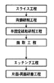
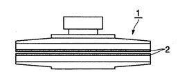
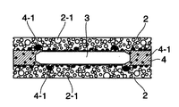
図1は本発明にかかる半導体ウェーハの製造方法の一実施例を示す製造工程図、図2は同じく本発明の他の実施例を示す製造工程図、図3は本発明の半固定砥粒研削工程で採用する両面研磨機の一例を示す概略図、図4は図3に示す両面研磨機のパッドにウエーハが押しつけられた状態の一部を拡大して示す断面図、図5は図4に示す状態においてスラリーが供給されて研削加工されている状態を示す図4相当図であり、1は両面研磨機、2は多孔質のパッド、3は半導体ウエーハ、4はスラリー、4−1は砥粒である。
【0013】
すなわち、本発明方法は図1に示すように、スライス工程後に、半固定砥粒研削工程、面取工程、エッチング工程、片面または両面研磨工程の各工程を順次行う方法であり、また、図2に示すように、スライス工程後に、両頭研削工程、半固定砥粒研削工程、面取工程、エッチング工程、片面または両面研磨工程の各工程を順次行う方法である。
【0014】
本発明の半固定砥粒研削工程で採用する両面研磨機1は、図3に示すように、1度に複数のウェーハを加工するバッチ式の研磨機1であって、ウェーハを挟む上下両面に多孔質のパッド2を貼付けている。この多孔質のパッドとしては、図4に示すように、例えば通常のポリシングで用いられる独立発泡性ポリウレタンパッドを用いることができる。ただし、その孔(ポア)2−1は使用する砥粒径に近いものが好ましく、例えば平均粒径が20μmの砥粒であれば、加工能率を考慮して孔径は10〜40μmが適当であり、また、硬度は90(JIS−A)以上のパッドの方が、ウエーハ表面のうねりを除去するのに有効である。なお、多孔質のパッドとしては、砥粒の粒径、加工能率、ウエーハ表面のうねり除去効果を考慮して、孔(ポア)径、硬度、さらには孔の形態(孔が独立したものが好ましい)や強度を選定し、その条件を満たすものを使用するもので、必ずしも発泡性ポリウレタンパッドに限定されない。
【0015】
また、研磨機としては、両面研磨機以外に、ラッピング装置、または比較的小さな定盤で1枚ずつ加工する枚葉式の装置を用いてもよい。さらには、半導体ウェーハの片面または両面について使用するものであってもよい。
【0016】
一方、砥粒としては、前記したように番手#400〜#1000程度(平均粒径11〜30μm)の遊離砥粒が適当であり、また砥粒の種類としてはGC、FO等のラッピング砥粒等が比較的安価でありこの加工法に利用することができる。また、砥粒の濃度としては、特に限定するものではないが、砥粒を多孔質状のパッド表面の孔(ポア)2−1に保持させることを考慮すると、2wt%以下の低濃度とするのが好ましい。
【0017】
図3に示す研磨機1において、図5に示すように、上下両面の多孔質のパッド2間に挟まれた半導体ウェーハ3が当該パッドにて押しつけられた状態で、該多孔質のパッド2に低濃度の遊離砥粒を懸濁したスラリー4を供給すると、パット表面の孔(ポア)2−1に砥粒4−1が保持され半固定砥粒として半導体ウェーハ3に対して研削作用(砥粒の引っ掻き作用)を生じる。そして、スラリー4を連続的に供給することにより、スラリー中の砥粒4−1はパッド表面にある程度保持されると脱落するため、研削砥石のような固定砥粒の目つぶれによる加工能率の低下を生じることはない。
【0018】
【実施例】
GC#800砥粒の濃度0.3wt%のスラリーを、発泡性ポリウレタンパンドを貼った両面研磨機(図3)に供給して半固定砥粒研削加工を行った結果、300mmウェーハにおいて、加工速度=2〜5μm/min、平坦度;TTV<1.0μmおよび表面粗さRa<400Åの半鏡面状態の半導体ウェーハを得ることができた。
また、当該加工法(半固定砥粒式研削)を図1、図2に示す製造工程に適用して半導体ウェーハを製造し、図7に示す従来の製造工程(プロセス)に対する取代の削減量と表面の微小うねり(ナノトポグラフィー)の結果を表1に示す。
表1の結果より明らかなごとく、従来工程(図7)での10mm□サイズでのナノトポグラフィー値24.9nmに対し、図1に示す製造工程では24.7nm、図2に示す製造工程では23.5nmとなり、取代を30〜35μm削減しても、従来の工程と同等の表面うねりの品質を得ることができた。
【表1】
【発明の効果】
以上説明したごとく、本発明方法によれば、スライス工程あるいは両頭研削工程で発生した半導体ウェーハ表面のうねりを、半固定砥粒研削工程により、ラッピング工程等と同等に除去することができるので、従来のラッピング工程、反転式平面研削工程を省略することができ、半導体ウェーハ製造プロセスを簡略化できるとともに加工取代を削減でき、また、スラリーを低濃度で供給することができるため消耗資材費を削減できる等、優れた効果を奏する。
【図面の簡単な説明】
【図1】 本発明にかかる半導体ウェーハの製造方法の一実施例を示す製造工程図である。
【図2】 本発明の他の実施例を示す製造工程図である。
【図3】 本発明の半固定砥粒研削工程で採用する両面研磨機の一例を示す概略図である。
【図4】 図3に示す両面研磨機のパッドにウエーハが押しつけられた状態の一部を拡大して示す断面図である。
【図5】 図4に示す状態において砥粒スラリーが供給されて研削加工されている状態を示す図4相当図である。
【図6】 従来の半導体ウェーハの製造方法の一例を示す製造工程図である。
【図7】 従来の半導体ウェーハの製造方法の一例を示す製造工程図である。
【符号の説明】
1 両面研磨機
2 多孔質のパッド
2−1 孔(ポア)
3 半導体ウエーハ
4 スラリー
4−1 砥粒[0001]
BACKGROUND OF THE INVENTION
The present invention relates to a method for obtaining a semiconductor wafer having high flatness and low processing strain from a single crystal ingot, and more specifically, a wire source while flattening a semiconductor wafer by semi-fixed abrasive grinding using loose abrasive grains. The present invention relates to a semiconductor wafer manufacturing method for reducing microscopic surface waviness generated by rice or double-head grinding and simplifying a conventional semiconductor wafer manufacturing process.
[0002]
[Prior art]
In general, a semiconductor wafer manufacturing method includes 1) a slicing step of slicing a single crystal ingot pulled by a single crystal pulling apparatus to obtain a thin disk-shaped wafer, and 2) a surface for preventing chipping or cracking of the wafer. Chamfering step, 3) lapping step for flattening the chamfered wafer, 4) etching step for removing the processing strain layer generated on the wafer by the above processing, and 5) chamfering polishing step for final polishing the chamfered portion, 6) A polishing step for polishing one or both sides of the wafer, and 7) a step for final polishing the wafer.
[0003]
Then, for the purpose of improving flatness and reducing minute surface waviness in the general semiconductor wafer manufacturing method as described above, as shown in FIG. 6, after the slicing step, chamfering step, and lapping step, A reversing surface grinding process is performed, an etching process for removing residual strain is performed as necessary, and a double-side polishing process is used (see Patent Document 1). As shown in FIG. After the chamfering process and lapping process, a reversing surface grinding process on both sides is performed, an etching process for removing residual strain is performed as necessary, and a single-sided or double-sided polishing process is performed (paragraph of Patent Document 2). Etc.) have been proposed.
[0004]
However, the lapping apparatus used in the lapping process in the conventional semiconductor wafer manufacturing method described above increases in size as the diameter of the wafer increases, leading to an increase in consumable materials and apparatus costs, an increase in wafer diameter, and a larger apparatus. Each of the problems such as an increase in the work load of the worker and an increase in industrial waste (waste abrasive powder) due to an increase in materials used have become prominent. In addition, when single-side grinding is performed immediately after slicing, there is a problem that waviness generated by a wire saw cannot be removed. As a means to solve this problem, various methods of manufacturing by replacing the lapping device with a double-headed grinding machine have been proposed, but the surface of the wafer manufactured by the double-headed grinding machine has a minute surface caused by double-headed grinding. There is a problem that waviness (number of elevation difference + μm, number of cycles mm) occurs. Accordingly, a method has been proposed in which the manufacturing process is simplified by lapping using an elastic surface plate after double-headed grinding in order to reduce micro-surface waviness and obtain a more uniform surface (described in Patent Document 2). Invention). However, in this method, the abrasive grains act softer than a metal surface plate and a wafer surface with less processing distortion can be obtained. However, the processing speed is low, and the elastic surface plate is significantly worn out to flatten the wafer. There is a problem that accuracy cannot be maintained.
[0005]
[Patent Document 1]
JP-A-9-246216 [Patent Document 2]
Japanese Patent Laid-Open No. 2002-124490 [0006]
[Problems to be solved by the invention]
The present invention has been made to solve the above-described problems of the prior art, and reduces the surface waviness caused by wire saw slicing or double-head grinding by semi-fixed abrasive grinding using loose abrasive grains. An object of the present invention is to provide a semiconductor wafer manufacturing method capable of simplifying a conventional semiconductor wafer manufacturing process.
[0007]
[Means for Solving the Problems]
The method for manufacturing a semiconductor wafer according to the present invention is a method for manufacturing a semiconductor wafer in which a chamfering process, an etching process, a single-sided or double-sided polishing process are performed after the slicing process, and the chamfering process is performed after the slicing process. Before, a semi-fixed abrasive grinding process is performed in which loose abrasive grains are held in the surface holes of the porous polishing pad and the surface of the polishing pad and the surface of the semiconductor wafer are in contact with each other to grind the surface of the semiconductor wafer. It is characterized by performing. Furthermore, prior to the slicing step after and semi fixed abrasive grinding process, you and performing double-disc grinding step of simultaneously ground by front and rear surfaces of the upper and lower grinding of a semiconductor wafer.
[0008]
The semi-fixed abrasive grinding process using the porous polishing pad and the loose abrasive grains in the present invention supplies, for example, loose abrasive grains having a count of # 400 to # 1000 at a low concentration to the porous polyurethane pad. In this way, the wafer is ground in a semi-fixed abrasive state with the abrasive grains held in the holes on the surface of the polishing pad. According to this method, since the wafer is ground by the scratching action of the abrasive grains held in a semi-fixed state on the pad surface, it is possible to reduce the micro waviness generated in the previous process such as slicing.
[0009]
In general, lapping is a process based on the brittle fracture action generated on the wafer surface due to the rolling of abrasive grains in the slurry layer between the wafer and the surface plate by supplying slurry with an abrasive concentration of about 20 wt% to the surface plate. Is the method. On the other hand, in the semi-fixed abrasive grinding in the present invention, the slurry layer is thinned by reducing the abrasive concentration in the slurry to about 1/10 of the conventional one, and the abrasive grains are made into pores on the porous pad surface ( This is based on a processing principle that causes the abrasive grain to be scratched by being held in the bore).
[0010]
Therefore, according to the method of the present invention, it is possible to obtain a good finished surface with high efficiency and relatively little processing distortion, and it is possible to remove the fine waviness on the surface generated in the slicing process or the double-head grinding process. In addition, since the abrasive concentration is reduced to about 1/10 of that of the conventional one, the amount of abrasive particles used is small, and it is possible to realize low cost by reducing consumable materials, and the abrasive concentration in the slurry. By making the concentration low, the polishing pad is not significantly worn and the flatness accuracy of the wafer can be maintained. Furthermore, the present invention can omit the conventional lapping step and the inversion surface grinding step by performing the semi-fixed abrasive grinding step after the slicing step, or after the slicing step and double-headed grinding step, It can be simplified.
[0011]
In addition, as a grinding means used in the semi-fixed abrasive grinding process of the present invention, a porous pad is attached to an existing apparatus such as a batch type double-side polishing machine or a lapping apparatus that processes a plurality of wafers at a time. Can be implemented.
[0012]
DETAILED DESCRIPTION OF THE INVENTION
FIG. 1 is a manufacturing process diagram showing an embodiment of a method of manufacturing a semiconductor wafer according to the present invention, FIG. 2 is a manufacturing process diagram showing another embodiment of the present invention, and FIG. 3 is a semi-fixed abrasive grinding according to the present invention. FIG. 4 is a schematic view showing an example of a double-side polishing machine employed in the process, FIG. 4 is an enlarged cross-sectional view showing a part of the wafer pressed against the pad of the double-side polishing machine shown in FIG. 3, and FIG. 4 is a view corresponding to FIG. 4 showing a state where the slurry is supplied and ground in the state shown in FIG. 1, 1 is a double-sided polishing machine, 2 is a porous pad, 3 is a semiconductor wafer, 4 is a slurry, 4-1 is an abrasive. It is a grain.
[0013]
That is, as shown in FIG. 1, the method of the present invention is a method of sequentially performing each process of a semi-fixed abrasive grinding process, a chamfering process, an etching process, a single-sided or double-sided polishing process after the slicing process. As shown in FIG. 2, after the slicing step, the double-sided grinding step, the semi-fixed abrasive grinding step, the chamfering step, the etching step, and the single-sided or double-sided polishing step are sequentially performed.
[0014]
The double-
[0015]
In addition to the double-side polishing machine, a lapping machine or a single-wafer type machine that processes each sheet with a relatively small surface plate may be used as the polishing machine. Furthermore, you may use about the single side | surface or both surfaces of a semiconductor wafer.
[0016]
On the other hand, the abrasive grains are free abrasive grains suitable for the above-described manner count # 400 # 1000 (average particle size 11~30Myuemu), and as the abrasive grains kind GC, lapping abrasive of FO like Grains and the like are relatively inexpensive and can be used in this processing method. Further, the concentration of the abrasive grains is not particularly limited, but considering that the abrasive grains are held in the pores (pores) 2-1 on the porous pad surface, the concentration is set to a low concentration of 2 wt% or less. Is preferred.
[0017]
In the polishing
[0018]
【Example】
As a result of supplying a slurry with a concentration of 0.3 wt% of GC # 800 abrasive grains to a double-side polishing machine (FIG. 3) to which a foaming polyurethane bond was applied, a semi-fixed abrasive grinding process was performed. = 2-5 μm / min, flatness; a semi-mirror surface semiconductor wafer with TTV <1.0 μm and surface roughness Ra <400 mm could be obtained.
Further, the processing method (semi-fixed abrasive type grinding) is applied to the manufacturing process shown in FIGS. 1 and 2 to manufacture a semiconductor wafer, and the reduction amount of the machining allowance with respect to the conventional manufacturing process (process) shown in FIG. Table 1 shows the results of surface micro-waviness (nanotopography).
Table 1 As a result more evident, to nanotopography value 24.9nm at 10 mm □ size in the conventional process (FIG. 7), in the manufacturing process shown in FIG. 1 is 24.7Nm, in the manufacturing process shown in FIG. 2 Even when the machining allowance was reduced by 30 to 35 μm, the surface waviness quality equivalent to that of the conventional process could be obtained.
[Table 1]
【The invention's effect】
As described above, according to the method of the present invention, the waviness on the surface of the semiconductor wafer generated in the slicing process or the double-headed grinding process can be removed by the semi-fixed abrasive grinding process in the same manner as in the lapping process. Lapping process and reversing surface grinding process can be omitted, the semiconductor wafer manufacturing process can be simplified, the machining allowance can be reduced, and the slurry can be supplied at a low concentration, thereby reducing the cost of consumable materials. Etc. have excellent effects.
[Brief description of the drawings]
FIG. 1 is a manufacturing process diagram showing an embodiment of a semiconductor wafer manufacturing method according to the present invention.
FIG. 2 is a manufacturing process diagram showing another embodiment of the present invention.
FIG. 3 is a schematic view showing an example of a double-side polishing machine employed in the semi-fixed abrasive grinding process of the present invention.
4 is an enlarged cross-sectional view showing a part of a state in which a wafer is pressed against a pad of the double-side polishing machine shown in FIG. 3;
5 is a view corresponding to FIG. 4 showing a state in which abrasive slurry is supplied and ground in the state shown in FIG. 4;
FIG. 6 is a manufacturing process diagram showing an example of a conventional method for manufacturing a semiconductor wafer.
FIG. 7 is a manufacturing process diagram showing an example of a conventional method for manufacturing a semiconductor wafer.
[Explanation of symbols]
1 Double-
Claims (2)
Priority Applications (6)
| Application Number | Priority Date | Filing Date | Title |
|---|---|---|---|
| JP2003149782A JP4345357B2 (en) | 2003-05-27 | 2003-05-27 | Manufacturing method of semiconductor wafer |
| KR1020057022726A KR100757287B1 (en) | 2003-05-27 | 2004-05-26 | Production method for semiconductor wafer |
| PCT/JP2004/007571 WO2004107428A1 (en) | 2003-05-27 | 2004-05-26 | Production method for semiconductor wafer |
| CNA200480014685XA CN1795545A (en) | 2003-05-27 | 2004-05-26 | Production method for semiconductor wafer |
| EP04734952A EP1632993A4 (en) | 2003-05-27 | 2004-05-26 | Production method for semiconductor wafer |
| US10/557,430 US20070023395A1 (en) | 2003-05-27 | 2004-05-26 | Production method for semiconductor wafer |
Applications Claiming Priority (1)
| Application Number | Priority Date | Filing Date | Title |
|---|---|---|---|
| JP2003149782A JP4345357B2 (en) | 2003-05-27 | 2003-05-27 | Manufacturing method of semiconductor wafer |
Publications (2)
| Publication Number | Publication Date |
|---|---|
| JP2004356231A JP2004356231A (en) | 2004-12-16 |
| JP4345357B2 true JP4345357B2 (en) | 2009-10-14 |
Family
ID=33487158
Family Applications (1)
| Application Number | Title | Priority Date | Filing Date |
|---|---|---|---|
| JP2003149782A Expired - Fee Related JP4345357B2 (en) | 2003-05-27 | 2003-05-27 | Manufacturing method of semiconductor wafer |
Country Status (6)
| Country | Link |
|---|---|
| US (1) | US20070023395A1 (en) |
| EP (1) | EP1632993A4 (en) |
| JP (1) | JP4345357B2 (en) |
| KR (1) | KR100757287B1 (en) |
| CN (1) | CN1795545A (en) |
| WO (1) | WO2004107428A1 (en) |
Families Citing this family (14)
| Publication number | Priority date | Publication date | Assignee | Title |
|---|---|---|---|---|
| CA2673660C (en) * | 2006-12-28 | 2012-07-24 | Saint-Gobain Ceramics & Plastics, Inc. | Sapphire substrates and methods of making same |
| US8740670B2 (en) | 2006-12-28 | 2014-06-03 | Saint-Gobain Ceramics & Plastics, Inc. | Sapphire substrates and methods of making same |
| US8455879B2 (en) * | 2006-12-28 | 2013-06-04 | Saint-Gobain Ceramics & Plastics, Inc. | Sapphire substrates and methods of making same |
| KR20140131598A (en) * | 2006-12-28 | 2014-11-13 | 생-고뱅 세라믹스 앤드 플라스틱스, 인코포레이티드 | A sapphire substrate |
| DE102007035266B4 (en) * | 2007-07-27 | 2010-03-25 | Siltronic Ag | A method of polishing a substrate of silicon or an alloy of silicon and germanium |
| TWI403575B (en) * | 2008-12-20 | 2013-08-01 | Cabot Microelectronics Corp | Composition for improving dryness during wire sawing |
| US9550264B2 (en) * | 2009-06-04 | 2017-01-24 | Sumco Corporation | Fixed abrasive-grain processing device, method of fixed abrasive-grain processing, and method for producing semiconductor wafer |
| DE102009025243B4 (en) * | 2009-06-17 | 2011-11-17 | Siltronic Ag | Method for producing and method of processing a semiconductor wafer made of silicon |
| DE102010005904B4 (en) * | 2010-01-27 | 2012-11-22 | Siltronic Ag | Method for producing a semiconductor wafer |
| CN103231302B (en) * | 2013-04-12 | 2015-04-29 | 同济大学 | Method for obtaining super-smooth surface low-sub-surface-damage crystal |
| CN103878660A (en) * | 2014-03-31 | 2014-06-25 | 高佳太阳能股份有限公司 | Silicon wafer grinding device used for silicon wafer treatment |
| CN105141812B (en) * | 2015-06-18 | 2022-02-11 | 重庆新知创科技有限公司 | Production method of sapphire camera window sheet |
| CN105141813B (en) * | 2015-06-18 | 2021-09-21 | 江苏苏创光学器材有限公司 | Preparation method of sapphire camera window sheet |
| US10410008B2 (en) * | 2016-03-08 | 2019-09-10 | Oracle International Corporation | Thick client policy caching |
Family Cites Families (15)
| Publication number | Priority date | Publication date | Assignee | Title |
|---|---|---|---|---|
| US4144099A (en) * | 1977-10-31 | 1979-03-13 | International Business Machines Corporation | High performance silicon wafer and fabrication process |
| JPS5789559A (en) * | 1980-11-25 | 1982-06-03 | Hitachi Ltd | Grinding surface plate |
| JPS5958827A (en) * | 1982-09-28 | 1984-04-04 | Toshiba Corp | Semiconductor wafer and method and apparatus for manufacturing semiconductor wafer |
| JPH01193167A (en) * | 1988-01-29 | 1989-08-03 | Toshiba Corp | Grinding/polishing device |
| JP3580600B2 (en) * | 1995-06-09 | 2004-10-27 | 株式会社ルネサステクノロジ | Method for manufacturing semiconductor device, semiconductor wafer used for the same, and method for manufacturing the same |
| US5967882A (en) * | 1997-03-06 | 1999-10-19 | Keltech Engineering | Lapping apparatus and process with two opposed lapping platens |
| JPH11135474A (en) * | 1997-10-30 | 1999-05-21 | Komatsu Electron Metals Co Ltd | Mirror-polished semiconductor wafer and its manufacture |
| JPH11154655A (en) | 1997-11-21 | 1999-06-08 | Komatsu Electron Metals Co Ltd | Manufacture of semiconductor wafer |
| JP2000218519A (en) * | 1999-02-02 | 2000-08-08 | Kanebo Ltd | Polishing material |
| JP2001102337A (en) * | 1999-09-28 | 2001-04-13 | Hitachi Cable Ltd | Semiconductor crystal wafer and polishing method therefor |
| US20020004358A1 (en) * | 2000-03-17 | 2002-01-10 | Krishna Vepa | Cluster tool systems and methods to eliminate wafer waviness during grinding |
| JP2002124490A (en) | 2000-08-03 | 2002-04-26 | Sumitomo Metal Ind Ltd | Method of manufacturing semiconductor wafer |
| JP4573492B2 (en) * | 2001-03-27 | 2010-11-04 | 株式会社東京ダイヤモンド工具製作所 | Synthetic whetstone |
| US7066801B2 (en) * | 2003-02-21 | 2006-06-27 | Dow Global Technologies, Inc. | Method of manufacturing a fixed abrasive material |
| US6910951B2 (en) * | 2003-02-24 | 2005-06-28 | Dow Global Technologies, Inc. | Materials and methods for chemical-mechanical planarization |
-
2003
- 2003-05-27 JP JP2003149782A patent/JP4345357B2/en not_active Expired - Fee Related
-
2004
- 2004-05-26 WO PCT/JP2004/007571 patent/WO2004107428A1/en active Application Filing
- 2004-05-26 EP EP04734952A patent/EP1632993A4/en not_active Withdrawn
- 2004-05-26 CN CNA200480014685XA patent/CN1795545A/en active Pending
- 2004-05-26 KR KR1020057022726A patent/KR100757287B1/en active IP Right Grant
- 2004-05-26 US US10/557,430 patent/US20070023395A1/en not_active Abandoned
Also Published As
| Publication number | Publication date |
|---|---|
| US20070023395A1 (en) | 2007-02-01 |
| KR100757287B1 (en) | 2007-09-11 |
| CN1795545A (en) | 2006-06-28 |
| KR20060024782A (en) | 2006-03-17 |
| WO2004107428A1 (en) | 2004-12-09 |
| JP2004356231A (en) | 2004-12-16 |
| EP1632993A4 (en) | 2006-07-05 |
| EP1632993A1 (en) | 2006-03-08 |
Similar Documents
| Publication | Publication Date | Title |
|---|---|---|
| JP4345357B2 (en) | Manufacturing method of semiconductor wafer | |
| TWI228066B (en) | Abrasive cloth dresser and method for dressing an abrasive cloth with the same | |
| JP2009124153A (en) | Method for producing semiconductor wafer with polished edge part | |
| JP5600867B2 (en) | Manufacturing method of semiconductor wafer | |
| SG170662A1 (en) | Method for producing a semiconductor wafer | |
| JP5493956B2 (en) | Manufacturing method of semiconductor wafer | |
| JP2009302409A (en) | Method of manufacturing semiconductor wafer | |
| TW201140678A (en) | Method for the double side polishing of a semiconductor wafer | |
| JP2002532898A (en) | Semiconductor wafer processing incorporating post-surface damage. | |
| JP2002124490A (en) | Method of manufacturing semiconductor wafer | |
| JP2009302410A (en) | Method of manufacturing semiconductor wafer | |
| JP2012094559A (en) | Planarization processing method for hard brittle wafer and pad for planarization processing | |
| TW201528356A (en) | Production method for mirror polished wafers | |
| JPH08236489A (en) | Manufacture of semiconductor wafer | |
| JP2007067179A (en) | Mirror-finished surface polishing method and system for semiconductor wafer | |
| JP2002231665A (en) | Method for manfuacturing semiconductor wafer with epitaxial film | |
| JP2010021394A (en) | Method of manufacturing semiconductor wafer | |
| JP2008303097A (en) | Manufacturing process of silicon carbide single crystal substrate | |
| CN110140195B (en) | Method for polishing silicon wafer, method for manufacturing silicon wafer, and silicon wafer | |
| JP2008188678A (en) | Double side polishing apparatus | |
| JP2007027488A (en) | Method for polishing semiconductor wafer | |
| JP2001007064A (en) | Grinding method of semiconductor wafer | |
| EP2192609A1 (en) | Method of producing wafer for active layer | |
| JP2002025950A (en) | Manufacturing method for semiconductor wafer | |
| TW200401405A (en) | Process for machining a wafer-like workpiece |
Legal Events
| Date | Code | Title | Description |
|---|---|---|---|
| A521 | Request for written amendment filed |
Free format text: JAPANESE INTERMEDIATE CODE: A523 Effective date: 20031210 |
|
| A621 | Written request for application examination |
Free format text: JAPANESE INTERMEDIATE CODE: A621 Effective date: 20050824 |
|
| A131 | Notification of reasons for refusal |
Free format text: JAPANESE INTERMEDIATE CODE: A131 Effective date: 20081017 |
|
| A521 | Request for written amendment filed |
Free format text: JAPANESE INTERMEDIATE CODE: A523 Effective date: 20081216 |
|
| A131 | Notification of reasons for refusal |
Free format text: JAPANESE INTERMEDIATE CODE: A131 Effective date: 20090313 |
|
| A521 | Request for written amendment filed |
Free format text: JAPANESE INTERMEDIATE CODE: A523 Effective date: 20090428 |
|
| TRDD | Decision of grant or rejection written | ||
| A01 | Written decision to grant a patent or to grant a registration (utility model) |
Free format text: JAPANESE INTERMEDIATE CODE: A01 Effective date: 20090623 |
|
| A01 | Written decision to grant a patent or to grant a registration (utility model) |
Free format text: JAPANESE INTERMEDIATE CODE: A01 |
|
| A61 | First payment of annual fees (during grant procedure) |
Free format text: JAPANESE INTERMEDIATE CODE: A61 Effective date: 20090706 |
|
| R150 | Certificate of patent or registration of utility model |
Ref document number: 4345357 Country of ref document: JP Free format text: JAPANESE INTERMEDIATE CODE: R150 Free format text: JAPANESE INTERMEDIATE CODE: R150 |
|
| FPAY | Renewal fee payment (event date is renewal date of database) |
Free format text: PAYMENT UNTIL: 20120724 Year of fee payment: 3 |
|
| FPAY | Renewal fee payment (event date is renewal date of database) |
Free format text: PAYMENT UNTIL: 20130724 Year of fee payment: 4 |
|
| R250 | Receipt of annual fees |
Free format text: JAPANESE INTERMEDIATE CODE: R250 |
|
| R250 | Receipt of annual fees |
Free format text: JAPANESE INTERMEDIATE CODE: R250 |
|
| R250 | Receipt of annual fees |
Free format text: JAPANESE INTERMEDIATE CODE: R250 |
|
| R250 | Receipt of annual fees |
Free format text: JAPANESE INTERMEDIATE CODE: R250 |
|
| R250 | Receipt of annual fees |
Free format text: JAPANESE INTERMEDIATE CODE: R250 |
|
| R250 | Receipt of annual fees |
Free format text: JAPANESE INTERMEDIATE CODE: R250 |
|
| R250 | Receipt of annual fees |
Free format text: JAPANESE INTERMEDIATE CODE: R250 |
|
| R250 | Receipt of annual fees |
Free format text: JAPANESE INTERMEDIATE CODE: R250 |
|
| R250 | Receipt of annual fees |
Free format text: JAPANESE INTERMEDIATE CODE: R250 |
|
| R250 | Receipt of annual fees |
Free format text: JAPANESE INTERMEDIATE CODE: R250 |
|
| LAPS | Cancellation because of no payment of annual fees |