JP4339030B2 - Self-excited switching power supply circuit oscillation control method - Google Patents
Self-excited switching power supply circuit oscillation control method Download PDFInfo
- Publication number
- JP4339030B2 JP4339030B2 JP2003189681A JP2003189681A JP4339030B2 JP 4339030 B2 JP4339030 B2 JP 4339030B2 JP 2003189681 A JP2003189681 A JP 2003189681A JP 2003189681 A JP2003189681 A JP 2003189681A JP 4339030 B2 JP4339030 B2 JP 4339030B2
- Authority
- JP
- Japan
- Prior art keywords
- voltage
- control
- oscillation
- turn
- output
- Prior art date
- Legal status (The legal status is an assumption and is not a legal conclusion. Google has not performed a legal analysis and makes no representation as to the accuracy of the status listed.)
- Expired - Lifetime
Links
Images


Landscapes
- Dc-Dc Converters (AREA)
Description
【0001】
【発明の属する技術分野】
本発明は、自励式スイッチング電源回路の発振制御方法に関し、更に詳しくは、トランスの一次巻線に流れる励磁電流を停止させた際に、二次出力巻線からトランスに蓄積されたエネルギーを放出するフライバック型自励式スイッチング電源回路の発振制御方法に関する。
【0002】
【従来の技術】
スイッチング電源回路は、安定化電源として、バッテリーチャージャーやACアダプタなどに用いられている。スイッチ素子の駆動方式(スイッチング方式)を大別すると、自励発振方式と他励発振方式とに分けられ、自励発振方式は、トランスなどのインダクタンス部品の帰還巻線に表れる電圧を、駆動信号としてスイッチ素子の制御端子に正帰還させ、発振動作を行うものである。
【0003】
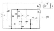
そのような自励式スイッチング電源回路の発振制御方法として、図6に示すような回路による制御方法が知られている(例えば、特許文献1参照)。
【0004】
以下、この従来の自励式スイッチング電源回路100の発振制御方法を、図6乃至図10を用いて説明すると、図中1は、電圧が変動する可能性のある不安定な直流電源であり、1aは、その高圧側端子、1bは、低圧側端子である。また、2aは、トランス2の一次巻線、2bは、トランス2の帰還巻線、2cは、トランス2の二次出力巻線であり、3は、発振用電界効果トランジスタ(以下、FETと記す)である。21は、回路起動時において、このFET3のゲートに順方向バイアス(換言すればスレッショルド電圧VTH以上のゲート電圧)を与えるために用いられている起動用抵抗であり、起動用抵抗21に直列に接続された電気抵抗25は、起動用抵抗21に対して小さい抵抗値であり、これにより直流電源1の電圧を分圧し、低い直流電圧が出力された場合には、回路が起動しないようにしたものである。
【0005】
6は、ゲートへの過大入力を防ぐツェナーダイオード、12は、帰還抵抗23とともにオン制御回路を構成し、帰還巻線2bとFET3のゲートとの間に直列に接続される帰還コンデンサ、24は、ゲートへの過大入力を阻止する為の電気抵抗、5は、コレクタをゲートへエミッタを低圧側端子1bへ接続した制御用トランジスタ素子である。また、22は、制御用コンデンサ11とともに発振安定化回路を構成する制御用抵抗であり、制御用コンデンサ11との接続点は、制御用トランジスタ素子5のベースに接続している。
【0006】
二次出力巻線2c側に示される4と13は、それぞれ、整流平滑化回路を構成する整流用ダイオード及び平滑コンデンサであり、二次出力巻線2cの出力を整流平滑化して、高圧側出力線20aと低圧側出力線20b間に出力する。
【0007】
この自励式スイッチング電源回路100の基本的な自励発振動作について説明すると、始めに、電源1の高圧側端子1aと低圧側端子1bに直流電圧が加えられると、起動用抵抗21を介して帰還コンデンサ12が充電され(図中下の電極が+で上が−の極性)、帰還コンデンサ12の充電電圧は、徐々に上昇する。
【0008】
帰還コンデンサ12の充電電圧がスレッショルド電圧VTHに達すると、FET3のゲートに順方向バイアス電圧が印加され、FET3がターンオンする(ドレイン−ソース間が導通する)。
【0009】
FET3がターンオンし、直列に接続された一次巻線2aに直流電源1から励磁電流が流れ始めると、トランス2の各巻線には誘導起電力が生じ、トランス2に励磁エネルギーが蓄積される。このとき、帰還巻線2bに発生した駆動信号としての電圧は、制御用抵抗22を介して制御用コンデンサ11を充電し、制御用トランジスタ5のベース電圧が上昇する(図7(a)のt12からt10)。
【0010】
また、t12からt10で表すFET3のオン期間中は、帰還巻線2bに発生する誘起電圧が、帰還コンデンサ12の充電電圧に重畳し、FET3のゲート電圧(図7(b))をそのスレッショルド電圧VTH以上の電圧に維持する。このとき、ツェナーダイオード6によって、ゲートへの過大入力が阻止される。
【0011】
制御用コンデンサ11が充電され、その充電電圧(制御用トランジスタ5のベース電圧)が所定のバイアス電圧以上に達する(図7(a)のt10)と、制御用トランジスタ5にべース電流が流れてコレクタ−エミッタ間が導通状態になる。その結果、FET3のゲートは、制御用トランジスタ5を介して実質的に低圧側端子1bと短絡状態となり(図7(b))、FET3はターンオフする。
【0012】
こうしてFET3がターンオフし、トランスに流れる電流が実質的に遮断されると、各巻線にはいわゆるフライバック電圧(誘導逆起電力)が生じる(図7(d)のt10からt11)。このとき、二次出力巻線2cに発生するフライバック電圧は、整流用ダイオード4とコンデンサ13とにより形成される平滑整流回路によって整流平滑化され、出力線20a、20b間に接続される負荷に供給される電力として出力される。
【0013】
一方、帰還巻線2bに発生するフライバック電圧は、出力側に接続された負荷により二次巻線2cに発生するフライバック電圧と比例関係にあり、この帰還巻線2bに発生するフライバック電圧によって、帰還コンデンサ12が充電される(図6において下の電極が+で上が一の極性)。
【0014】
このとき、ツェナーダイオード6は、FET3のゲートに逆バイアスをかけ、かつ、低圧端子1b側から帰還コンデンサ12を充電する充電電流のパスとして作用する。
【0015】
誘導逆起電力によって二次出力巻線2cに蓄積されていた電気的エネルギの放出が終わる(図7(d)のt11時)と、ゲートに対して逆バイアスとして作用していた帰還巻線2bのフライバック電圧が降下し、それまで帰還コンデンサ12に保持されていた充電電圧により、FET3のゲート電圧がスレッショルド電圧VTHを越え(図7(b)のt12)、FET3が再びターンオンし、このようにして一連の発振動作が繰り返される。
【0016】
このように自励発振する自励式スイッチング電源回路100において、トランス2の二次側には、出力線20a、20b間の電圧を監視し、FET3のオンデューティを変化させ、出力線20a、20b間の出力電圧を安定化させる回路が備えられている。
【0017】
すなわち、高圧側出力線20aと低圧側出力線20bとの間には、2つの分圧抵抗30、31が直列に接続され、その中間タップ32を、誤差増幅器33の反転入力端子に接続することにより、反転入力端子に出力電圧の分圧を入力している。また、誤差増幅器33の非反転入力端子と低圧側出力線20bの間には、基準電源34が接続され、非反転入力端子に、出力電圧の分圧と比較するための基準電圧を入力している。
【0018】
誤差増幅器33の出力側には、フォトカプラ発光素子35が接続され、フォトカプラ発光素子35は、電気抵抗36を介して高圧側出力線20aに接続することによって、駆動電源の供給を受けている。尚、直列に接続された電気抵抗37とコンデンサ38は、誤差増幅器33を安定動作させるための交流負帰還素子である。
【0019】
一方、一次側の起動用抵抗21の一側(FET3のゲート側)と制御用トランジスタ5のベース間には、フォトカプラ発光素子35とフォトカップルするフォトカプラ受光素子39が接続されている。
【0020】
これらの回路構成によって、例えば、高圧側出力線20aと低圧側出力線20b間の出力電圧が所定の設定電圧(例えば、6V)より上昇すると、誤差増幅器33の反転入力端子に入力される分圧も上昇し、基準電圧との電位差が反転増幅され、フォトカプラ発光素子35の発光しきい値を越える電位となる。
【0021】
その結果、フォトカプラ発光素子35は発光し、フォトカプラ受光素子39が受光することにより、フォトカプラ受光素子39はオン動作状態となる。ターンオフ工程の後、トランス2の帰還巻線2bに発生するフライバック電圧は、逆バイアス状態のツェナーダイオード6からオン動作状態となっているフォトカプラ受光素子39を経由して、制御用コンデンサ11を充電する。帰還巻線2bに発生するフライバック電圧により制御用コンデンサ11は、逆方向に充電されるが(図6において上が−で下が+の極性)、フォトカプラ受光素子39の電流によって、この逆方向の電圧は小さくなり、図7(a)のt12時の電圧値は高くなる。従って、直後のFET3がターンオンしてから制御用トランジスタ5のベースが動作電圧に達するまでの時間、すなわちオン時間(図7(c)のt12からt10間)が減少することによって、トランス2に蓄積されるエネルギーが減少し、出力電圧が低下する。
【0022】
逆に、出力電圧が設定電圧より低下すると、フォトカプラ発光素子35は、発光しないので、起動用抵抗21の一側と制御用トランジスタ5のベース間は、遮断され、制御用コンデンサ11の充電は、制御用抵抗22を介してのみ行われる。従って、充電時間は遅れ、FET3のオン時間が増加し、出力電圧は上昇し、このように発振制御を行うことにより、出力電圧を設定電圧とする定電圧制御が行われる。
【0023】
つまり、この従来の自励式スイッチング電源回路100の発振制御方法では、出力線20a、20b間に、重い負荷(消費電力が大きい負荷)が接続された場合には、出力電圧が低下するので、FET3のオン時間がより長くなるように、逆に軽負荷(消費電力の小さい負荷)が接続された場合には、出力電圧が上昇するので、FET3のオン時間が短縮されるように、発振制御される。
【0024】
図8は、出力線20a、20b間に、自励式スイッチング電源回路100の定格より軽い負荷が接続された場合の図7の各動作波形をより長い時間連続して表したもので、連続発振によりトランス2に蓄積されるエネルギーが負荷により消費されるエネルギーを上回ることとなった例えば図中Ta時には、ターンオフ後の出力電圧が設定電圧を越えているので、次の発振の際のオン時間が短縮される。一次巻線2aに流れる最大励磁電流は、ほぼFET3のオン時間に比例する(図7(c)参照)ので、オン時間が短縮されれば、発生するフライバック電圧も低下し、ターンオフしてからフライバック電圧が消失するまでのエネルギー放出時間が短くなり、オフ時間が短縮される。
【0025】
つまり、オン時間とオフ時間ともに短縮していくので発振周波数が上昇し、この現象は出力電圧が設定電圧以下とならない限り連続し、結局、次の発振を起動できない程度にオン時間が短縮した図8のTb時で発振が停止する。
【0026】
自励発振が停止したTb後であっても、出力線20a、20b間の出力電圧が設定電圧を越えている間は、フォトカプラ受光素子39が受光することにより、制御用トランジスタ5はオン動作し、これによってFET3のゲート電圧はスレッショルド電圧以下に保たれ、FET3はターンオンしない。
【0027】
出力線20a、20b間に接続された負荷によりエネルギーが消費され、出力電圧が徐々に低下し設定電圧以下となると、フォトカプラ受光素子39は受光しなくなるので、既述したように、起動用抵抗21を介して帰還コンデンサ12が充電され、帰還コンデンサ12の充電電圧がスレッショルド電圧VTHに達することにより、図8のTc時に再びFET3がターンオンする。
【0028】
図9は、Tc時の起動後の図7の各動作波形を拡大して表したもので、起動直後は、制御用コンデンサ11が充電されていないので、制御用トランジスタ5のベース電圧は、ほぼ接地電位であり、ターンオン後に発生する励磁電圧によってすぐに制御トランジスタ5がオン動作し、FET3はターンオフする。つまり、オン時間が非常に短く、その結果ターンオフ後に発生するフライバック電圧も低圧で消失するまでのオフ時間も短い。しかし、フライバック電圧が発生することにより、制御用コンデンサ11は、逆方向に充電され(図6において上が−で下が+の極性)、制御用トランジスタ5のベースには、逆バイアスがかかった状態となる。従って、次の発振において、FET3がターンオンしてから制御用トランジスタ5のベースが動作電圧に達するまでの時間、すなわちオン時間はより長くなり、オン時間が長くなることによりフライバック電圧の消失時間、すなわちオフ時間も長くなる。
【0029】
このようにオン時間とオフ時間が共に長くなり、発振周期が長くなる現象は、図8、図9に示すように、出力電圧が設定電圧を越え出力電圧の制御が開始されるTa時まで連続する。
【0030】
つまり、定格より軽い負荷が出力線20a、20b間に接続している限り、Tc時からTb時までの発振動作と、Tb時からTc時までの休止動作を繰り返し、これをより長い時間間隔でみれば、出力電圧は、図10に示すように、設定電圧である6Vを頂点に変動し、発振動作中のTc時からTb時に上昇し、休止動作中のTb時からTc時に下降する。
【0031】
又、他の従来の発振制御方法として、補助電源を用いて帰還コンデンサ12を充電し、出力の実効値低下を防止する図11に示す回路200による制御方法が知られている(例えば、特許文献2参照)。
【0032】
図11に示す自励式スイッチング電源回路200は、図6に示す電源回路100と基本動作は同一であるので、対応する構成には同一番号を付し、異なる構成と作用について以下に説明する。
【0033】
この自励式スイッチング電源回路200の発振制御方法では、一次巻線2aに励磁電流が流れるオン時間中は、帰還巻線2bに生じる誘起電圧によって、電気抵抗40と整流ダイオード41を介して補助コンデンサ44を充電する。その後、FET3がターンオフし、一次巻線2aの励磁電流が停止するオフ時間中は、オン時間中に補助コンデンサ44に充電されていた充電電圧によって、整流ダイオード42と電気抵抗43を介して帰還コンデンサ12を充電する。
【0034】
これにより、消費電力を低減させるため高い抵抗値の起動用抵抗21を介して帰還コンデンサ12を充電する場合でも、補助コンデンサ44からも充電を受けるので、短時間に充電し、オン動作に復帰させることができる。
【0035】
【特許文献1】
特開2002−51546号
【特許文献2】
特開2001−327164
【0036】
【発明が解決しようとする課題】
従来の自励式スイッチング電源回路100の発振制御方法では、自励発振の周波数が出力電圧に応じて周期的に変化し、特に発振周波数が上昇する図8のTa時からTb時にかけては、自励式スイッチング電源回路100全体でのエネルギー損失が多くなり、伝達効率が低下するものとなる。
【0037】
また、出力側では、発振動作と休止動作を繰り返す間欠発振動作となる為に、出力電圧に図10に示すようなリプル電圧が発生し、ノイズの原因となるという問題があった。
【0038】
更に、自励式スイッチング電源回路200の発振制御方法では、補助電源を用いて帰還コンデンサ12を充電するものであるが、過剰な充電電流が発生した場合には、オフ時間中であってもFET3のゲートがスレッショルド電圧VTH以上となり、フライバック電圧が消失するまでオフ動作すべきFET3がスイッチ素子としての機能を果たさなくなるという問題があった。
【0039】
本発明はこのような問題点に鑑みてなされたもので、軽い負荷が出力線に接続されても、自励発振の周波数が上昇することがなく、エネルギー損失が少ない自励式スイッチング電源回路の発振制御方法を提供することを目的とする。
【0040】
また、間欠発振動作に移行せず、ノイズの原因となるリプル電圧が発生しない自励式スイッチング電源回路の発振制御方法を提供することを目的とする。
【0041】
また、補助電源を用いて帰還コンデンサを充電する場合であっても、発振用主スイッチ素子が誤動作しない自励式スイッチング電源回路の発振制御方法を提供することを目的とする。
【0042】
【課題を解決するための手段】
請求項1の自励式スイッチング電源回路の発振制御方法は、直流電源に対してトランスの一次巻線と直列に接続した発振用主スイッチ素子の制御端子にオン制御電圧を加え、発振用主スイッチ素子をターンオンさせて一次巻線に励磁電流を流すターンオン工程と、ターンオン工程の後、一次巻線に直列に接続する抵抗に、前記励磁電流を流し、抵抗の両端に発生する電圧で、抵抗と閉ループを形成する制御用コンデンサを充電し、発振用主スイッチ素子の制御端子と直流電源の低圧側端子間に接続された副スイッチ素子の副制御端子電圧を、副制御端子に接続する制御用コンデンサの充電電圧でオン制御電圧として副スイッチ素子をオン制御し、制御端子の電圧をオフ制御電圧とし、発振用主スイッチ素子をターンオフさせて一次巻線に流れる励磁電流を停止するターンオフ工程と、ターンオフ工程の後、トランスの二次出力巻線に発生するフライバック電圧を整流平滑化し、出力線へ出力電圧として出力する出力工程とを備え、ターンオフ工程の後、トランスの帰還巻線に発生するフライバック電圧で帰還コンデンサを充電するとともに、制御用コンデンサの充電電圧を閉ループを形成する抵抗へ放電し、副制御端子電圧をオフ制御電圧として副スイッチ素子をオフ制御した後、帰還コンデンサの充電電圧を発振用主スイッチ素子の制御端子へ正帰還させ、制御端子をオン制御電圧に引き上げ、再びターンオン工程から各工程を繰り返す自励式スイッチング電源回路の発振制御方法であって、
ターンオフ工程の後、出力電圧を所定の設定電圧と比較し、出力電圧が所定の設定電圧を越えている間は、トランスのいずれかの巻線に発生するフライバック電圧で充電される駆動用コンデンサの充電電圧を副制御端子に加えて副スイッチ素子をオン制御し、出力電圧が設定電圧以下となったときに、駆動用コンデンサと副制御端子を遮断し、オン制御している副スイッチ素子をオフ制御し、ターンオン工程へ移行させることを特徴とする。
【0043】
軽負荷が出力線間に接続している場合には、ターンオフ工程の後、二次出力巻線に発生するフライバック電圧が消失した後も、出力電圧は設定電圧を越え、出力電圧が設定電圧を越えている間は、トランスのいずれかの巻線に発生するフライバック電圧で充電される駆動用コンデンサの充電電圧が副制御端子に加わり、副制御端子電圧をオン制御電圧に保つので、副スイッチ素子がオン制御され、発振用主スイッチ素子はターンオンせず、ターンオン工程に移行しない。
【0044】
負荷の電力消費により出力電圧が設定電圧以下となると、制御用コンデンサの充電電圧が閉ループを形成する抵抗へ放電され、副制御端子電圧がオフ制御電圧となり副スイッチ素子がオフ制御され、発振用主スイッチ素子の制御端子は、帰還コンデンサの充電電圧でオン制御電圧に引き上げられ、発振用主スイッチ素子がターンオンして、ターンオン工程に移行する。
【0045】
出力線に接続される負荷の重さにより、個々の発振周期において次の発振の為の発振用主スイッチ素子のターンオンまでの時間が調整され、軽い負荷が接続された場合であっても発振周波数は上昇しない。
【0046】
また、トランスに蓄積されるエネルギーも、各発振周期で負荷の重さにかかわらず一発振周期内に消費されるので、出力電圧が低下せずに間欠発振動作に移行することがなく、リプル電圧が発生しない。
【0047】
また、少なくともフライバック電圧が消滅するまでは、副スイッチ素子がオン制御され、発振用主スイッチ素子の制御端子は、オン制御電圧に引き上げられることがないので、帰還コンデンサに過剰な充電電流が流れても、発振用主スイッチ素子は誤動作しない。
【0048】
請求項2の自励式スイッチング電源回路の発振制御方法は、出力線に許容最大消費電力の負荷が接続された状態で、フライバック電圧が消失した時に、出力電圧が設定電圧以下となり、ターンオン工程へ移行するように、オン時間及び/又は設定電圧を調整することを特徴とする。
【0049】
トランスに発生する電力は、ターンオフした際に一次巻線に流れる励磁電流の二乗に比例し、この励磁電流はオン時間に略比例して上昇するので、オン時間により、トランスに発生する電力を調整できる。
【0050】
出力線に接続可能な負荷の最大消費電力とトランスに発生する電力が釣り合うようにオン時間を調整すれば、フライバック電圧が消失した時に出力電圧が低下する。従って、オン時間と設定電圧のいずれか一方、若しくは双方を調整することによって、フライバック電圧が消失した時に、出力電圧を設定電圧以下とすることができ、最も重い負荷が接続された状態で、オフ調整時間Tadを設けることなく速やかにターンオン工程に移行させることができる。
【0051】
また、許容最大消費電力の負荷に対して軽い負荷を出力線に接続した場合には、フライバック電圧が消失してから、出力電圧が設定電圧以下に低下するまでのオフ調整時間Tadが経過した後、ターンオン工程に移行する。
【0052】
請求項3の自励式スイッチング電源回路の発振制御方法は、直流電源に対してトランスの一次巻線と直列に接続した発振用電界効果トランジスタのゲート電圧をスレッショルド電圧VTH以上に引き上げ、発振用電界効果トランジスタをターンオンさせて一次巻線に励磁電流を流すターンオン工程と、ターンオン工程の後、一次巻線に直列に接続する抵抗に、前記励磁電流を流し、抵抗の両端に発生する電圧で、抵抗と閉ループを形成する制御用コンデンサを充電し、発振用電界効果トランジスタのゲートと直流電源の低圧側端子間に接続された制御用トランジスタのベース電圧を、ベースに接続する制御用コンデンサの充電電圧でオン制御電圧として制御用トランジスタをオン制御し、ゲート電圧をスレッショルド電圧VTH未満とし、発振用電界効果トランジスタをターンオフさせて一次巻線に流れる励磁電流を停止するターンオフ工程と、ターンオフ工程の後、トランスの二次出力巻線に発生するフライバック電圧を整流平滑化し、出力線へ出力電圧として出力する出力工程とを備え、ターンオフ工程の後、トランスの第1帰還巻線に発生するフライバック電圧で帰還コンデンサを充電するとともに、制御用コンデンサの充電電圧を閉ループを形成する抵抗へ放電し、制御用トランジスタのベース電圧をオフ制御電圧として制御用トランジスタをオフ制御した後、帰還コンデンサの充電電圧を発振用電界効果トランジスタのゲートへ正帰還させ、ゲート電圧をスレッショルド電圧VTHに引き上げ、再びターンオン工程から各工程を繰り返す自励式スイッチング電源回路の発振制御方法であって、
ターンオフ工程の後、トランスの第2帰還巻線に発生するフライバック電圧で駆動用コンデンサを充電し、出力電圧が所定の設定電圧を越えている間、トランスの二次側のフォトカプラ発光素子を発光し、フォトカップルするトランスの一次側のフォトカプラ受光素子を動作させ、第2帰還巻線に発生するフライバック電圧若しくは動用コンデンサの充電電圧を制御用トランジスタのベースに加えて、制御用トランジスタをオン制御し、出力電圧が設定電圧以下となったときに、フォトカプラ受光素子の動作を停止させ、第2帰還巻線に発生するフライバック電圧若しくは動用コンデンサの充電電圧を制御用トランジスタのベースから遮断し、制御用トランジスタをオフ制御し、ターンオン工程へ移行させることを特徴とする。
【0053】
出力線に接続された負荷が軽い場合には、フライバック電圧が低下した後も、整流平滑化した出力線の電位低下が遅く高電圧を保つので、フォトカプラ受光素子が動作し、制御用トランジスタをオン制御する。その結果、フライバック電圧が低下し、帰還コンデンサの充電電位が発振用電界効果トランジスタのゲート電圧をスレッショルド電圧VTH以上に引き上げターンオンするタイミングとなっても、第2帰還巻線に発生するフライバック電圧若しくは駆動用コンデンサの充電電圧が制御用トランジスタのベースに加わり、ベース電圧をオン制御電圧に保ち、制御用トランジスタが実質的に発振用電界効果トランジスタのゲートと低圧側端子間を短絡するので、発振用電界効果トランジスタはターンオン工程に移行しない。
【0054】
負荷の電力消費により、出力電圧が設定電圧以下となると、フォトカプラ受光素子の動作が停止し、制御用コンデンサの充電電圧が閉ループを形成する抵抗へ放電され、ベース電圧がオフ制御電圧となるので、制御用トランジスタはオフ制御され、その結果、帰還コンデンサの充電電位が発振用電界効果トランジスタのゲート電圧をスレッショルド電圧VTH以上に引き上げ、ターンオン工程に移行する。
【0055】
従って、各発振毎に、ターンオンのタイミングを遅らせるオフ調整時間Tadが発生するが、軽い負荷が接続されても、発振周波数は上昇しない。
【0056】
また、個々の発振毎に、負荷の大きさに応じて、トランスに蓄えられるエネルギーが次の発振を遅らせることにより調整されるので、間欠発振に移行せず、リプル電圧が発生しない。
【0057】
また、少なくともフライバック電圧が消滅するまでは、制御用トランジスタがオン制御され、発振用電界効果トランジスタのゲート電圧はスレッショルド電圧VTH以上に引き上げられることがないので、帰還コンデンサに過剰な充電電流が流れても、発振用電界効果トランジスタが誤動作しターンオンすることはない。
【0058】
請求項4の自励式スイッチング電源回路の発振制御方法は、第1帰還巻線の両側に、発振用電界効果トランジスタのゲートを介して直列に接続される制御用トランジスタと帰還コンデンサが接続することにより閉ループが形成され、ターンオフ工程の後、トランスの第1帰還巻線に発生するフライバック電圧で充電される帰還コンデンサは、オン制御される制御用トランジスタのエミッタ、コレクタ間に流れる充電電流で充電されることを特徴とする。
【0059】
発振用電界効果トランジスタの動作を制御する制御用トランジスタが、ターンオフ後に発生するフライバック電圧で帰還コンデンサを充電する充電パスを兼ねるので、フライバック電圧による充電電流が流れ、ターンオン工程では、逆方向の放電を阻止する整流ダイオード等による充電経路を別に設ける必要がない。
【0060】
フライバック電圧が消失した後に、制御用トランジスタがオン動作している場合であっても、制御用トランジスタを介して閉ループを、自由振動による充、放電電流が流れるので、充電電位は緩やかに低下する。その結果、帰還コンデンサの充電電位は、少なくとも出力電圧が設定電圧以下に低下するまで、ゲート電圧をスレッショルド電圧VTH以上に引き上げられる電位に保たれる。
【0061】
【発明の実施の形態】
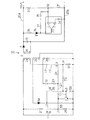
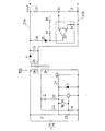
以下、本発明の一実施の形態について、図1乃至図5を用いて詳細に説明する。図1は、本発明の一実施の形態に係る発振制御方法を行うための自励式スイッチング電源回路10の構成を示す回路図である。本実施の形態に係る自励式スイッチング電源回路10は、図6で示した従来の自励式スイッチング電源回路100と主要な回路及び回路素子が共通するものであるので、同一の構成には同一の番号を付けて、その説明を省略する。
【0062】
図1に示すように、トランス2は、一次側に一次巻線2aと、一次巻線2aと同一方向に巻回された第1帰還巻線2b、及び一次巻線2aと逆方向に巻回され第2帰還巻線2dが配設され、二次側に二次出力巻線2cが配設されている。
【0063】
一次巻線2aは、直流電源1に対して、発振用主スイッチ素子を構成する発振用電界効果型トランジスタ(以下、FETという)3と直列に接続され、FET3のオンオフ動作により、一次巻線2aに流れる励磁電流がオンオフ制御される。
【0064】
FET3は、ここではMOSFETが用いられ、ドレインを一次巻線2aに接続し、ソースを一次電流検出抵抗51を介して直流電源1の低圧側端子1bに接続している。
【0065】
また、ゲートは、直流電源1に対して直列に接続された起動用抵抗21と電気抵抗25の接続点J1に、ゲートへの過大入力を阻止する電気抵抗24を介し接続している。起動用抵抗21と電気抵抗25のそれぞれの抵抗値は、1.5MΩと100kΩであり、これにより200V前後の不安定な直流電源1の電源電圧が著しく低下した場合には、FET3のゲート電圧がスレッショルド電圧VTHに達することなく、発振動作しないようになっている。
【0066】
接続点J1と第1帰還巻線2bの間には、オン制御回路を構成する帰還コンデンサ12及び帰還抵抗23が直列に接続され、第1帰還巻線2bの他側は、直流電源1の低圧側端子1bに接続している。
【0067】
また接続点J1と低圧側端子1b間には、FET3のゲート電圧をスレッショルド電圧VTH未満に低下させターンオフさせる副スイッチ素子となる制御用トランジスタ5が配置されている。ここでは、制御用トランジスタ5として、コレクタを接続点J1へ、エミッタを低圧側端子1bへ接続させたNPN型トランジスタを用いている。
【0068】
第2帰還巻線2dの一側は、直列に接続された整流ダイオード54と駆動用コンデンサ55を介して直流電源1の低圧側端子1bに接続し、また他側は、直接直流電源1の低圧側端子1bに接続し、これにより閉ループが形成されている。
【0069】
整流ダイオード54は、駆動用コンデンサ55の充電方向を順方向として配設され、これにより第2帰還巻線2dに発生するフライバック電圧で駆動用コンデンサ55が充電されるようになっている。
【0070】
整流ダイオード54と駆動用コンデンサ55の接続点J2は、フォトカプラ受光素子39と制御用コンデンサ53を介して低圧側端子1bに接続し、フォトカプラ受光素子39と制御用コンデンサ53の直列接続点J3を制御用トランジスタ5のベースへ接続している。
【0071】
直列接続点J3、すなわち制御用トランジスタ5のベースは、電気抵抗52を介して、FET3と一次電流検出抵抗51の接続点J4へも接続し、一次電流検出抵抗51による電圧降下が一定値以上となると、ベース電圧が上昇し、制御用トランジスタ5がオン動作するようになっている。
【0072】
フォトカプラ受光素子39は、トランス2の二次側のフォトカプラ発光素子35とフォトカップルして動作するもので、ここではフォトカプラ発光素子35からの光を受光した際に、接続点J2からJ3へその受光量に比例した電流を流すように動作する。
【0073】
トランスの二次出力巻線2cは、二次出力巻線2cと直列に整流用ダイオード4と、二次出力巻線2cと並列に平滑コンデンサ13が接続され、出力側の整流平滑化回路を構成している。
【0074】
この自励式スイッチング電源回路10においては、出力線20a、20b間の出力電圧を監視し、所定の設定電圧(本実施の形態では6V)との比較結果をフォトカプラ発光素子35からトランスの一次側のフォトカプラ受光素子39へ出力する比較回路が備えられている。
【0075】
すなわち、整流平滑回路の高圧側出力線20aと低圧側出力線20bとの間に、分圧抵抗30、31が直列に接続され、その中間タップ32を、誤差増幅器33の反転入力端子に接続し、反転入力端子に出力電圧の分圧となる出力検出電圧を入力している。また、誤差増幅器33の非反転入力端子と低圧側出力線20bの間には、基準電源34が接続され、非反転入力端子に、出力検出電圧と比較する基準電圧を入力している。基準電圧は、出力電圧を制御しようとする所定値に設定された設定電圧に対し、出力電圧と出力検出電圧の分圧比と同一比率の電圧で、出力検出電圧と基準電圧を比較することで、出力電圧を設定電圧と比較している。
【0076】
誤差増幅器33の出力側には、電気抵抗36を介して高圧側出力線20aに接続し、誤差増幅器33の出力値により点滅するフォトカプラ発光素子35が接続され、このフォトカプラ発光素子35は、前述したように一次側のフォトカプラ受光素子39とフォトカップリングしている。
【0077】
中間タップ32と誤差増幅器33の非反転入力端子間には、誤差増幅器33の出力との間に交流負帰還素子37、38が接続されている。
【0078】
尚、自励式スイッチング電源回路10では、更に出力線20a、20bに流れる出力電流を監視し、出力電流制御も行っているが、説明の都合上省略する。
【0079】
以下、このように構成された自励式スイッチング電源回路10の発振制御方法について説明する。
【0080】
始めに、電源回路10を起動してから出力電圧が制御されながら自励発振するまでの過渡状態での制御について説明する。この過渡状態では、出力線20a、20b間の出力電圧が後述する設定電圧に満たないので、フォトカプラ35、39は動作していない。
【0081】
電源回路10の起動直後は、直流電源1の高圧側端子1a、低圧側端子1b間に200V程度の直流電圧が発生しているので、起動用抵抗21と電気抵抗25で分圧された電源電圧により、起動用抵抗21と帰還抵抗23を介して、帰還コンデンサ12が充電される(図1において下の電極が+で上が−の極性)。
【0082】
充電される帰還コンデンサ12の充電電圧が、徐々に上昇し、FET3のスレッショルド電圧VTHに達すると、FET3のゲートに順方向バイアス電圧が印加され、FET3がターンオンし、ドレイン−ソース間が導通する。
【0083】
FET3がターンオンし、直列に接続された一次巻線2aに直流電源1から励磁電流が流れ始めると、トランス2の各巻線に誘導起電力が生じ、トランス2にエネルギーが蓄積される。帰還巻線2bに発生する誘起電圧は、帰還コンデンサ12の充電電圧と重畳され、FET3のゲート電圧をそのスレッショルド電圧VTH以上の電圧(オン制御電圧)に維持する。
【0084】
このとき、一次巻線2aに流れる励磁電流により一次電流検出抵抗51のFET3側、接続点J4に発生する電圧は、電気抵抗52を介して制御用コンデンサ53を充電する。一次巻線2aに流れる励磁電流は、ターンオン後の時間と共にほぼ直線的に上昇し、これにより制御用コンデンサ53の充電電圧も上昇する。
【0085】
制御用トランジスタ5のベース電圧がバイアス電圧に達すると、コレクタ−エミッタ間が導通状態になり、FET3のゲートは制御用トランジスタ5によって実質的に短絡状態(ここでは低圧側端子1bの電位で、例えば0ボルト)となり、FET3がターンオフする。
【0086】
FET3がターンオフし、トランス2に流れる電流が実質的に遮断されると、各巻線にはいわゆるフライバック電圧(誘導逆起電力)が生じる。このとき、二次出力巻線2cに発生するフライバック電圧は、整流用ダイオード4とコンデンサ13とにより形成される平滑整流回路によって整流平滑化され、負荷が接続される出力線20a、20b間に出力電圧として出力される。
【0087】
一方、第1帰還巻線2bに発生するフライバック電圧は、出力線20a、20b間に接続された負荷により二次巻線2cに発生するフライバック電圧と比例関係にあり、この第1帰還巻線2bに発生するフライバック電圧によって、帰還コンデンサ12が充電され(図1において下の電極が+で上が一の極性)、次のFET3のターンオンが導かれる。
【0088】
一方、FET3がターンオフした後は、一次巻線電流が停止するので、接続点J4の電圧は、接地電位に低下し、また、フォトカプラ受光素子39が動作していないので、制御用コンデンサ53の充電電圧は、電気抵抗52を介した放電により低下する。従って、制御用トランジスタ5のベース電圧は、バイアス電圧以下となっている。
【0089】
しかしながら、帰還コンデンサ12は、制御用トランジスタ5のベース、コレクタ間が等価ダイオードとして作用し、一次電流検出抵抗51から電気抵抗52、制御用トランジスタ5のベースからコレクタ、帰還抵抗23を、充電電流の経路として第1帰還巻線2bから充電される。
【0090】
誘導逆起電力によって二次出力巻線2cに蓄積されていた電気的エネルギの放出が終わると、一次巻線2aの電圧は、FET3の寄生容量、一次巻線2a間の浮遊容量及び一次巻線2aのインダクタンスによって電源電圧200Vを中心とした自由振動を開始し、電圧降下と共にその極性が反転する。
【0091】
一次巻線電圧の自由振動に比例して振動する第1帰還巻線2bの帰還コンデンサ12側の電圧も同様に変化し、ゲートに対して逆バイアスとして作用していたフライバック電圧が消滅した後に極性が反転し、FET3のゲートに対して順方向のバイアス電圧として作用するようになる。また、それまでに充電された帰還コンデンサ12の充電電圧が加わり、FET3のゲート電圧がスレッショルド電圧VTHを越えて、FET3が再びターンオンし、このようにして一連の自励発振動作を繰り返される。
【0092】
一度の発振周期でトランス2に蓄積されるエネルギーは、FET3のオン時間、すなわち、ターンオンしてから制御用トランジスタ5のベース電圧がバイアス電圧に達するまでの時間の二乗にほぼ比例し、フォトカプラ35、39は動作していないので、ベース電圧の上昇に関与せず、一次電流検出抵抗51の抵抗値により定まる最大オン時間で動作する。その結果、出力電圧は設定電圧に達するまで発振を繰り返す毎に上昇し、設定電圧を越えると、出力電圧を設定電圧と比較して制御する通常発振動作に移行する。
【0093】
この通常発振動作は、以下、出力線20a、20b間に接続される負荷の大きさにより異なるので、始めに、自励式スイッチング電源回路10の出力線20a、20b間に、許容最大消費電力の負荷が接続された場合の発振制御方法を、図1と図2で説明する。許容最大消費電力の負荷とは、自励式スイッチング電源回路10の直流電源電圧、各回路定数から、出力線20a、20b間に接続可能な最も消費電力の大きい負荷であり、自励式スイッチング電源回路10の出力定格として予め定められる。
【0094】
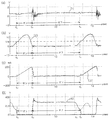
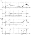
図2は、図7に対応し、それぞれ許容最大消費電力の負荷を接続して自励発振動作中の各部の波形を示すもので、図2(a)は、直列接続点J3の電圧、すなわち制御用トランジスタ5のベース電圧波形(1)を、図2(b)は、FET3のゲート電圧波形(2)を、図2(c)は、FET3のドレイン電流、すなわち一次巻線2aに流れる一次巻線電流波形(3)を、図2(d)は、FET3のドレイン電圧波形(4)をそれぞれ示している。
【0095】
本実施の形態では、出力線20a、20b間に許容最大消費電力の負荷を接続して自励発振動作をさせた場合に、フライバック電圧が消失した時(図2(d)のt1時)に出力電圧が設定電圧以下となるように、オン時間(図2(a)のt2からt0間)と設定電圧を調整している。
【0096】
すなわち、トランス2に発生する電力は、ターンオフした際に一次巻線2aに流れる励磁電流の二乗に比例し、この励磁電流はオン時間に略比例するので、許容最大消費電力とトランス2に発生する電力が釣り合うようにオン時間を調整すれば、フライバック電圧が消失した時に出力電圧が低下する。従って、オン時間と設定電圧のいずれか一方、若しくは双方を調整することによって、フライバック電圧が消失した時に、出力電圧が設定電圧以下となるように設定できる。
【0097】
FET3がターンオンした後のオン時間(図2(c)のt2からt0間)中は、出力電圧が上記調整により設定した設定電圧以下であり、フォトカプラー35、39は動作せず、過渡状態と同様に、一次巻線2aに流れる励磁電流による一次電流検出抵抗51の電圧降下が制御用トランジスタ5のバイアス電圧に達っした時(図2(a)のt0)に、制御用トランジスタ5がオン動作する。すなわち、一次電流検出抵抗51の抵抗値で定まる最大励磁電流が一次巻線2aに流れたときに、FET3はターンオフするので、一次電流検出抵抗51の抵抗値で調整されるオン時間(図2(c)のt2からt0間)は一定である。
【0098】
FET3がオン時間経過後ターンオフすることにより、二次出力巻線2cに発生するフライバック電圧は、平滑整流回路4、13で整流平滑化され出力線20a、20b間に出力電圧として出力され、これにより出力電圧は上昇し設定電圧を越える。
【0099】
高圧側出力線20aと低圧側出力線20b間の出力電圧が設定電圧を越えると、誤差増幅器33の反転入力端子に入力される中間タップ32の分圧も上昇し、基準電源34の基準電圧との電位差が反転増幅され、フォトカプラ発光素子35の発光しきい値を越える電位となる。
【0100】
その結果、フォトカプラ発光素子35は発光し、フォトカプラ受光素子39が受光することにより、接続点J2から接続点J3(制御用トランジスタ5のベース)へ受光量に比例した電流を流す。すなわち、フライバック電圧は、第2帰還巻線2dにも発生し、整流ダイオード54に順方向に働くので、フォトカプラ受光素子39を介して制御用コンデンサ53を充電し、制御用トランジスタ5のベース電圧を、バイアス電圧以上に保ち、制御用トランジスタ5はFET3がターンオフした後もオン動作を継続している。
【0101】
図2(a)に示すように、制御用トランジスタ5は、FET3がターンオフしたt0時に、ベース電圧が0.6Vのバイアス電圧に達し、コレクタとエミッタは導通して共にほぼ接地電位となっているが、FET3がターンオフした後も、出力電圧が設定電圧を超えている間は、ベース電圧がバイアス電圧以上の電圧を保っている。
【0102】
制御用トランジスタ5のベース電圧がバイアス電圧に達している間は、コレクタとエミッタ間は導通しているので、第1帰還巻線2bに発生するフライバック電圧により、制御用トランジスタ5のエミッタからコレクタ、帰還抵抗23を充電電流の経路として帰還コンデンサ12が充電される(図1において下の電極が+で上が一の極性)。
【0103】
また、帰還コンデンサ12が充電されている間、制御用トランジスタ5のベース電圧がバイアス電圧に達し、FET3のゲートと低圧側端子1bが実質的に短絡しているので、補助電源などを用いて帰還コンデンサ12が過剰に充電されることがあっても、ゲート電圧がスレッショルド電圧VTHに達することはなく、誤ってFET3がターンオンすることはない。
【0104】
許容最大消費電力の負荷が接続されている場合には、フライバック電圧が消失した時((図2(d)のt1時))に、出力電圧が設定電圧以下となるので、フォトカプラ発光素子35の発光が停止し、フォトカプラ受光素子39の受光動作が停止する。
【0105】
その結果、制御用コンデンサ53の充電電圧は、電気抵抗52、一次電流検出抵抗51を介して放電され、制御用コンデンサ53がオフ動作し、極性が反転した第1帰還巻線2bの電圧に、帰還コンデンサ12の充電電圧が加わり、FET3のゲート電圧がスレッショルド電圧VTHを越え、ほぼフライバック電圧が消失した時(図2のt2時)にFET3が再びターンオンする。
【0106】
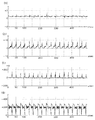
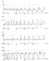
次に、出力線20a、20b間に接続される負荷が、より軽い(消費電力の小さい)負荷である場合の自励式スイッチング電源回路10の発振制御方法を、図1と図3乃至図5を用いて説明する。
【0107】
最も重い負荷が接続された状態でオン時間と設定電圧を調整した自励式スイッチング電源回路10の出力線20a、20b間に、より軽い(消費電力の小さい)負荷を接続すると、負荷による電力消費が少なくなるので、平滑整流回路4、13で整流平滑化された出力電圧の負荷による電位低下が遅く、フライバック電圧が消失した後も設定電圧を越えた高電圧となっている。
【0108】
そこで、本実施の形態では、出力電圧が設定電圧以下に低下するまで、次の自励発振の為のターンオンを遅らせ、各発振周期毎にトランス2で発生させる電力を負荷により消費される電力に合わせて調整するものである。
【0109】
FET3がターンオンした後のオン時間(図4のt3時からt0時)中は、出力電圧が設定電圧以下であり、フォトカプラ受光素子39は受光動作していないので、負荷の重さにかかわらず、FET3がターンオフするまでのオン時間は、一定である。
【0110】
図4に示すように、t0時にFET3がターンオフすると、各巻線に発生したフライバック電圧が発生し、トランス2の二次側でフライバック電圧を整流平滑化した出力電圧も上昇し、設定電圧を越える。
【0111】
フライバック電圧が発生している間の動作も、出力線20a、20bに接続されている負荷の重さにかかわらず同じで、前述と同様にフォトカプラ受光素子39がフォトカプラ発光素子35は発光して動作することにより、制御用コンデンサ53が充電され、制御用トランジスタ5はFET3がターンオフした後もオン動作を継続している。
【0112】
従って、帰還コンデンサ12は、制御用トランジスタ5を充電パスとして、第1帰還巻線2bに発生するフライバック電圧により充電されするとともに、帰還コンデンサ12が充電されている間、FET3のゲートと低圧側端子1bが実質的に短絡しているので、補助電源などを用いて帰還コンデンサ12が過剰に充電されることがあっても、ゲート電圧がスレッショルド電圧VTHに達することはなく、FET3はターンオフした状態を維持している。
【0113】
二次出力巻線2cに発生したフライバック電圧は、整流平滑化した出力電圧となり、図4のt1時に消失するが、許容最大消費電力の負荷より軽い負荷が接続されている場合には、フライバック電圧の消失後も出力電圧(すなわち、平滑コンデンサ13の両端の電圧)が設定電圧を越えた高電圧を保ち、フォトカプラ発光素子35は発光を継続している。これにより、制御用トランジスタ5はオン動作を継続し、帰還コンデンサ12がFET3のゲート電圧をスレッショルド電圧VTH以上とする充電電圧となっているにもかかわらず、FET3はターンオンしない。
【0114】
従って、図4(d)に示すように、t1時の後、一次巻線2aの電圧は、FET3の寄生容量、一次巻線2a間の浮遊容量及び一次巻線2aのインダクタンスによって電源電圧200Vを中心とした自由振動を開始する。自由振動は、巻線比に比例して、第1帰還巻線2bにも発生し(図4(b)参照)、帰還コンデンサ12はこの自由振動により充放電を繰り返すので、制御用トランジスタ5はオン動作を継続していても、フライバック電圧による充電電圧は、緩やかに低下するだけである。
【0115】
新たな発振がないので、負荷による電力消費で出力電圧は徐々に低下し、オフ調整時間Tadが経過したt3時に出力電圧が設定電圧以下となったとすると、フォトカプラ発光素子35は発光を停止し、フォトカプラ受光素子39の受光動作が停止する。
【0116】
その結果、制御用コンデンサ53の充電電圧は、電気抵抗52、一次電流検出抵抗51を介して放電され、制御用トランジスタ5がオフ動作し、第1帰還巻線2bの電圧に帰還コンデンサ12の充電電圧が加わり、FET3のゲート電圧がスレッショルド電圧VTHを越え、FET3がターンオンする。
【0117】
このように負荷の重さにより、各発振周期でオフ調整時間Tadを設けて、発振によりトランス2に発生するエネルギーと負荷により消費されるエネルギーのバランスをとるので、図3に示すように負荷の重さが変化しなければ略等しい周期で連続発振し、間欠発振に移行することがない。
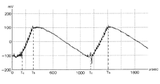
【0118】
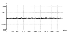
従って、出力電圧は、設定電圧をここでは6Vとしているので、ほぼ直流6Vの電圧となる。図5は、この本実施の形態による出力電圧波形を、従来の発振制御方法による出力電圧波形を表す図10と同じ時間間隔で対応させて示すもので、従来方法では、200mvの振幅のリプル電圧が表れているのに対し、本実施の形態の制御方法では、リプル電圧が全く表れないほぼ直流波形となっている。
【0119】
この実施の形態によれば、制御用トランジスタ5を充電パスとして帰還コンデンサ12を充電したが、他の充電パスを設けて充電してもよい。
【0120】
また、第2帰還巻線2dに発生するフライバック電圧で、駆動用コンデンサ55を充電しているが、第2帰還巻線2dは必ずしも設けることなく、一次巻線2a若しくは第1帰還巻線2bに、整流ダイオード54と駆動用コンデンサ55を直列に接続し、これらの巻線に発生するフライバック電圧で駆動用コンデンサ55を充電してもよい。
【0121】
また、上述の実施の形態では、許容最大消費電力の負荷を接続して自励発振動作をさせた場合に、ほぼフライバック電圧が消失するt1時(実際にはt2時)に出力電圧が設定電圧以下となるように、オン時間と設定電圧を調整したが、フライバック電圧が消失した後(t2時の後)に出力電圧が設定電圧以下となるものであってもよい。
【0122】
更に、上述の実施の形態では、重さ(消費電力)の異なる負荷が接続された場合を比較して説明したが、消費電力が変化する負荷が接続されている場合にも適用できることはいうまでもなく、この場合には、変化する負荷に応じて各発振周期毎に異なる長さのオフ調整時間Tadが設けられ、連続した自励発振動作を行う。
【0123】
【発明の効果】
以上説明したように、本発明によれば、軽い負荷が出力線に接続されても、自励発振の周波数が上昇することがなく、エネルギーの損失が少ない。
【0124】
また、間欠発振動作に移行することがないので、ノイズの原因となるリプル電圧が発生しない。
【0125】
更に、フライバック電圧が発生している間、副スイッチ素子(制御用コンデンサ)が、制御端子(ゲート)と低圧側端子を実質的に短絡させているので、帰還コンデンサが過充電される場合であっても、発振用主スイッチ素子(発振用電界効果トランジスタ)は確実にオフ動作を維持する。
【0126】
これに加えて、請求項2の発明では、最も重い負荷が接続された場合に、無駄ない発振周期で自励発振を連続させ、負荷が軽くなるにつれてオフ調整時間Tadを設けて、発振周波数を低下させるので、自励発振の際のスイッチング等によるエネルギー損失を最小限に押さえることができる。
【0127】
また、請求項4の発明では、制御用トランジスタが、ターンオフ後に発生するフライバック電圧で帰還コンデンサを充電する充電パスを兼ねるので、充電経路を別に設ける必要がない。
【図面の簡単な説明】
【図1】 本発明の一実施の形態に係る発振制御方法を行うための自励式スイッチング電源回路10の構成を示す回路図である。
【図2】 許容最大消費電力の負荷を接続して自励発振動作中の自励式スイッチング電源回路10の各部の波形を示し、
(a)は、制御用トランジスタ5のベース電圧波形(1)を、
(b)は、FET3のゲート電圧波形(2)を、
(c)は、FET3のドレイン電流波形(3)を、
(d)は、FET3のドレイン電圧波形(4)を
それぞれ示す波形図である。
【図3】 軽い負荷を接続し自励発振動作中の図2の各部の波形を比較的長い時間間隔で示し、
(a)は、制御用トランジスタ5のベース電圧波形(1)を、
(b)は、FET3のゲート電圧波形(2)を、
(c)は、FET3のドレイン電流波形(3)を、
(d)は、FET3のドレイン電圧波形(4)を
それぞれ示す波形図である。
【図4】 軽い負荷を接続し自励発振動作中の図2の各部の波形を図3より拡大して示し、
(a)は、制御用トランジスタ5のベース電圧波形(1)を、
(b)は、FET3のゲート電圧波形(2)を、
(c)は、FET3のドレイン電流波形(3)を、
(d)は、FET3のドレイン電圧波形(4)を
それぞれ示す波形図である。
【図5】 軽い負荷を接続し自励発振動作中の出力電圧波形を表す長い時間間隔で表す波形図である。
【図6】 従来の自励式スイッチング電源回路100の回路図である。
【図7】 自励発振動作を行っている従来の自励式スイッチング電源回路100の各部の波形を図2に対応させて示し、
(a)は、制御用トランジスタ5のベース電圧波形を、
(b)は、FET3のゲート電圧波形を、
(c)は、FET3のドレイン電流波形を、
(d)は、FET3のドレイン電圧波形を
それぞれ示す波形図である。
【図8】 図7の各部の波形を図3に対応させて示し、
(a)は、制御用トランジスタ5のベース電圧波形を、
(b)は、FET3のゲート電圧波形を、
(c)は、FET3のドレイン電流波形を、
(d)は、FET3のドレイン電圧波形を
それぞれ示す波形図である。
【図9】 間欠発振を行い、発振を開始した自励式スイッチング電源回路100の各部の波形を拡大し、
(a)は、制御用トランジスタ5のベース電圧波形を、
(b)は、FET3のゲート電圧波形を、
(c)は、FET3のドレイン電流波形を、
(d)は、FET3のドレイン電圧波形を
それぞれ示す波形図である。
【図10】 従来の自励式スイッチング電源回路100の自励発振動作中の出力電圧波形を図5に対応させて示す波形図である。
【図11】 他の従来の自励式スイッチング電源回路200の回路図である。
【符号の説明】
1 直流電源
1a 高圧側端子
1b 低圧側端子
2 トランス
2a 一次巻線
2b 帰還巻線(第1帰還巻線)
2c 二次出力巻線
2d 第2帰還巻線
3 発振用電界効果トランジスタ(発振用主スイッチ素子)
5 制御用トランジスタ(副スイッチ素子)
10 自励式スイッチング電源回路
12 帰還コンデンサ
35 フォトカプラ発光素子
39 フォトカプラ受光素子
55 駆動用コンデンサ [0001]
BACKGROUND OF THE INVENTION
The present invention relates to an oscillation control method for a self-excited switching power supply circuit, and more specifically, releases energy stored in a transformer from a secondary output winding when the exciting current flowing in the primary winding of the transformer is stopped. The present invention relates to an oscillation control method for a flyback self-excited switching power supply circuit.
[0002]
[Prior art]
The switching power supply circuit is used for a battery charger, an AC adapter, or the like as a stabilized power supply. Switching device driving methods (switching methods) can be broadly divided into self-excited oscillation methods and separately-excited oscillation methods. The self-excited oscillation method uses the voltage that appears in the feedback winding of an inductance component such as a transformer as the drive signal. Is positively fed back to the control terminal of the switch element to oscillate.
[0003]
As a method for controlling the oscillation of such a self-excited switching power supply circuit, a control method using a circuit as shown in FIG. 6 is known (for example, see Patent Document 1).
[0004]
Hereinafter, the oscillation control method of the conventional self-excited switching
[0005]
6 is a Zener diode that prevents an excessive input to the gate, 12 is an on-control circuit together with the
[0006]
[0007]
The basic self-oscillation operation of the self-excited switching
[0008]
The charging voltage of the
[0009]
When the
[0010]
T12To t10During the ON period of the
[0011]
The
[0012]
When the
[0013]
On the other hand, the flyback voltage generated in the feedback winding 2b is proportional to the flyback voltage generated in the
[0014]
At this time, the Zener
[0015]
Release of the electrical energy accumulated in the secondary output winding 2c is terminated by the induced back electromotive force (t in FIG. 7D).11) And the flyback voltage of the feedback winding 2b acting as a reverse bias with respect to the gate drops, and the gate voltage of the
[0016]
In the self-excited switching
[0017]
That is, two
[0018]
A photocoupler
[0019]
On the other hand, a photocoupler light-receiving
[0020]
With these circuit configurations, for example, when the output voltage between the high-voltage
[0021]
As a result, the photocoupler
[0022]
On the other hand, when the output voltage drops below the set voltage, the photocoupler
[0023]
In other words, in this conventional oscillation control method of the self-excited switching
[0024]
FIG. 8 shows each operation waveform of FIG. 7 continuously for a longer time when a load lighter than the rating of the self-excited switching
[0025]
In other words, both the on-time and off-time are shortened, so the oscillation frequency increases, and this phenomenon continues as long as the output voltage does not fall below the set voltage, and eventually the on-time is shortened to the extent that the next oscillation cannot be started. Oscillation stops at 8 Tb.
[0026]
Even after Tb when the self-excited oscillation is stopped, while the output voltage between the
[0027]
When energy is consumed by the load connected between the
[0028]
FIG. 9 is an enlarged view of each operation waveform of FIG. 7 after startup at Tc. Since the
[0029]
The phenomenon that both the on time and the off time become longer and the oscillation period becomes longer as shown in FIGS. 8 and 9 continues until Ta when the output voltage exceeds the set voltage and control of the output voltage is started. To do.
[0030]
In other words, as long as a load lighter than the rating is connected between the
[0031]
As another conventional oscillation control method, there is known a control method using the
[0032]
Since the basic operation of the self-excited switching
[0033]
In this oscillation control method of the self-excited switching
[0034]
As a result, even when the
[0035]
[Patent Document 1]
JP 2002-51546 A
[Patent Document 2]
JP 2001-327164 A
[0036]
[Problems to be solved by the invention]
In the conventional oscillation control method of the self-excited switching
[0037]
Further, on the output side, there is a problem that a ripple voltage as shown in FIG. 10 is generated in the output voltage due to the intermittent oscillation operation in which the oscillation operation and the pause operation are repeated, causing noise.
[0038]
Further, in the oscillation control method of the self-excited switching
[0039]
The present invention has been made in view of such problems. Even when a light load is connected to the output line, the frequency of the self-excited oscillation does not increase, and the oscillation of the self-excited switching power supply circuit has low energy loss. An object is to provide a control method.
[0040]
Another object of the present invention is to provide an oscillation control method for a self-excited switching power supply circuit that does not shift to an intermittent oscillation operation and does not generate a ripple voltage that causes noise.
[0041]
Another object of the present invention is to provide an oscillation control method for a self-excited switching power supply circuit in which the oscillation main switch element does not malfunction even when the feedback capacitor is charged using an auxiliary power supply.
[0042]
[Means for Solving the Problems]
The oscillation control method for a self-excited switching power supply circuit according to
After the turn-off process, the output voltage is compared with a predetermined set voltage,While the output voltage exceeds the specified set voltage, the charging voltage of the driving capacitor charged with the flyback voltage generated in one of the windings of the transformer is added to the sub control terminal to turn on the sub switch element. AndWhen the output voltage falls below the set voltage,Shut off the driving capacitor and the sub-control terminal,The sub-switch element that is on-controlled is controlled to be off and shifted to a turn-on process.
[0043]
When a light load is connected between the output lines, the output voltage exceeds the set voltage even after the flyback voltage generated in the secondary output winding disappears after the turn-off process. WhileSince the charging voltage of the driving capacitor charged with the flyback voltage generated in one of the windings of the transformer is added to the sub-control terminal, the sub-control terminal voltage is kept at the on-control voltage,Sub switch element is on-controlledAndThe oscillation main switch element does not turn on and does not enter the turn-on process.
[0044]
When the output voltage falls below the set voltage due to load power consumption,The charging voltage of the control capacitor is discharged to the resistor that forms the closed loop, and the sub-control terminal voltage becomes the off-control voltage.The sub switch element is turned off, the control terminal of the oscillation main switch element is pulled up to the on control voltage by the charging voltage of the feedback capacitor, the oscillation main switch element is turned on, and the process proceeds to the turn-on process.
[0045]
Depending on the weight of the load connected to the output line, the time until turn-on of the oscillation main switch element for the next oscillation is adjusted in each oscillation period, and even if a light load is connected, the oscillation frequency Does not rise.
[0046]
The energy stored in the transformer is also consumed within one oscillation period regardless of the load weight in each oscillation period, so the output voltage does not decrease and transition to intermittent oscillation operation does not occur. Does not occur.
[0047]
Also, at least until the flyback voltage disappears, the sub-switch element is on-controlled, and the control terminal of the oscillation main switch element is not pulled up to the on-control voltage, so an excessive charging current flows through the feedback capacitor. However, the oscillation main switch element does not malfunction.
[0048]
In the oscillation control method for the self-excited switching power supply circuit according to
[0049]
The power generated in the transformer is proportional to the square of the excitation current flowing in the primary winding when it is turned off, and this excitation current rises in proportion to the on-time, so the power generated in the transformer is adjusted by the on-time. it can.
[0050]
If the on-time is adjusted so that the maximum power consumption of the load that can be connected to the output line is balanced with the power generated in the transformer, the output voltage will drop when the flyback voltage disappears. Therefore, by adjusting one or both of the on-time and the set voltage, when the flyback voltage disappears, the output voltage can be made lower than the set voltage, and with the heaviest load connected, OFF adjustment time TadWithout being provided, it is possible to promptly shift to the turn-on process.
[0051]
Further, when a light load is connected to the allowable maximum power consumption load on the output line, the off adjustment time T from when the flyback voltage disappears until the output voltage drops below the set voltage.adAfter elapses, the process proceeds to the turn-on process.
[0052]
The oscillation control method for a self-excited switching power supply circuit according to claim 3 is characterized in that a gate voltage of an oscillation field effect transistor connected in series with a primary winding of a transformer with respect to a DC power supply is a threshold voltage VTHAfter pulling up the above, after turning on the oscillation field effect transistor and passing the exciting current to the primary winding, and after the turn-on process,The exciting current is passed through a resistor connected in series to the primary winding, and the control capacitor that forms a closed loop with the resistor is charged with a voltage generated across the resistor,Connected between the gate of the oscillation field-effect transistor and the low-voltage side terminal of the DC power supplyThe base voltage of the control transistor is turned on by the charge voltage of the control capacitor connected to the base.The control transistor is turned on, and the gate voltage is set to the threshold voltage VTHThe turn-off process of turning off the field effect transistor for oscillation to stop the exciting current flowing in the primary winding, and the rectifying and smoothing of the flyback voltage generated in the secondary output winding of the transformer after the turn-off process and output Output step to output to the line as an output voltage, and after the turn-off step, charge the feedback capacitor with the flyback voltage generated in the first feedback winding of the transformerIn addition, the charging voltage of the control capacitor is discharged to a resistor that forms a closed loop, and the base voltage of the control transistor is used as an off-control voltage.After the control transistor is turned off, the charging voltage of the feedback capacitor is positively fed back to the gate of the oscillation field effect transistor, and the gate voltage is changed to the threshold voltage VTHIs an oscillation control method for a self-excited switching power supply circuit that repeats each process from the turn-on process to
After the turn-off process, the flyback voltage generated in the second feedback winding of the transformerDriving capacitorWhile the output voltage exceeds the preset voltage, turn the photocoupler light-emitting element on the secondary side of the transformerFlashOperate the photocoupler light-receiving element on the primary side of the photocoupler to operate the flyback voltage generated in the second feedback winding orDynamic capacitorIs added to the base of the control transistor, and the control transistor is turned on. When the output voltage falls below the set voltage, the operation of the photocoupler light receiving element is stopped and generated in the second feedback winding. Flyback voltage orDynamic capacitorThe charging voltage is cut off from the base of the control transistor, the control transistor is controlled to be turned off, and the process proceeds to the turn-on process.
[0053]
When the load connected to the output line is light, even after the flyback voltage drops, the potential drop of the rectified and smoothed output line slows down and maintains a high voltage, so the photocoupler light-receiving element operates and the control transistor Turn on the control. As a result, the flyback voltage decreases, and the charging potential of the feedback capacitor changes the gate voltage of the oscillation field effect transistor to the threshold voltage VTHEven when it is time to turn up and turn onThe flyback voltage generated in the second feedback winding or the charging voltage of the driving capacitor is applied to the base of the control transistor, and the base voltage is kept at the on control voltage,Since the control transistor substantially short-circuits between the gate of the oscillation field effect transistor and the low-voltage side terminal, the oscillation field effect transistor does not enter the turn-on process.
[0054]
When the output voltage falls below the set voltage due to the power consumption of the load, the operation of the photocoupler light receiving element stops,The charging voltage of the control capacitor is discharged to the resistor that forms the closed loop, and the base voltage becomes the off-control voltage.Control transistorIsOFF controlIsAs a result, the charging potential of the feedback capacitor changes the gate voltage of the oscillation field effect transistor to the threshold voltage VTHPull up to the above and move to the turn-on process.
[0055]
Therefore, the off adjustment time T for delaying the turn-on timing for each oscillation.adHowever, the oscillation frequency does not increase even when a light load is connected.
[0056]
Further, for each oscillation, the energy stored in the transformer is adjusted by delaying the next oscillation according to the magnitude of the load, so that the oscillation does not shift to the intermittent oscillation and no ripple voltage is generated.
[0057]
Further, at least until the flyback voltage disappears, the control transistor is turned on, and the gate voltage of the oscillation field effect transistor is the threshold voltage VTHSince it is not pulled up more than that, even if an excessive charging current flows through the feedback capacitor, the oscillation field effect transistor will not malfunction and turn on.
[0058]
The oscillation control method for a self-excited switching power supply circuit according to
[0059]
The control transistor that controls the operation of the oscillating field effect transistor also serves as a charging path for charging the feedback capacitor with the flyback voltage generated after turn-off, so that a charge current flows due to the flyback voltage. There is no need to provide a separate charging path with a rectifier diode or the like for preventing discharge.
[0060]
Even when the control transistor is turned on after the flyback voltage disappears, the charging potential gradually decreases because the charge and discharge currents flow through the closed loop through the control transistor due to free vibration. . As a result, the charging potential of the feedback capacitor is changed from the gate voltage to the threshold voltage V at least until the output voltage drops below the set voltage.THThe potential is raised to the above.
[0061]
DETAILED DESCRIPTION OF THE INVENTION
Hereinafter, an embodiment of the present invention will be described in detail with reference to FIGS. FIG. 1 is a circuit diagram showing a configuration of a self-excited switching
[0062]
As shown in FIG. 1, the
[0063]
The primary winding 2a is connected to the
[0064]
Here, MOSFET is used as the
[0065]
Further, the gate is connected to a connection point J1 of the starting
[0066]
Between the connection point J1 and the first feedback winding 2b, a
[0067]
Further, the gate voltage of the
[0068]
One side of the second feedback winding 2d is connected to the low-
[0069]
The
[0070]
The connection point J2 between the
[0071]
The series connection point J3, that is, the base of the
[0072]
The photocoupler light-receiving
[0073]
The secondary output winding 2c of the transformer includes a rectifying
[0074]
In this self-excited switching
[0075]
That is, the
[0076]
The output side of the
[0077]
AC
[0078]
In the self-excited switching
[0079]
Hereinafter, an oscillation control method of the self-excited switching
[0080]
First, control in a transient state from when the
[0081]
Immediately after the
[0082]
The charging voltage of the
[0083]
When the
[0084]
At this time, the voltage generated on the
[0085]
When the base voltage of the
[0086]
When the
[0087]
On the other hand, the flyback voltage generated in the first feedback winding 2b is proportional to the flyback voltage generated in the secondary winding 2c by the load connected between the
[0088]
On the other hand, since the primary winding current stops after the
[0089]
However, the
[0090]
When the electrical energy accumulated in the secondary output winding 2c is terminated by the induced back electromotive force, the voltage of the primary winding 2a is changed to the parasitic capacitance of the
[0091]
The voltage on the
[0092]
The energy accumulated in the
[0093]
Since this normal oscillation operation is different depending on the size of the load connected between the
[0094]
FIG. 2 corresponds to FIG. 7 and shows the waveforms of the respective parts during the self-excited oscillation operation by connecting the load of the maximum allowable power consumption, and FIG. 2 (a) shows the voltage at the series connection point J3, that is, FIG. 2 (b) shows the gate voltage waveform (2) of the
[0095]
In the present embodiment, when a self-excited oscillation operation is performed by connecting a load having a maximum allowable power consumption between the
[0096]
That is, the power generated in the
[0097]
ON time after the
[0098]
When the
[0099]
When the output voltage between the high-voltage
[0100]
As a result, the photocoupler
[0101]
As shown in FIG. 2 (a), the
[0102]
While the base voltage of the
[0103]
Further, while the
[0104]
When a load with the maximum allowable power consumption is connected, the flyback voltage disappears ((t in FIG. 2 (d)1)), The output voltage becomes equal to or lower than the set voltage, so that the light emission of the photocoupler
[0105]
As a result, the charging voltage of the
[0106]
Next, the oscillation control method of the self-excited switching
[0107]
When a lighter load (low power consumption) is connected between the
[0108]
Therefore, in this embodiment, the turn-on for the next self-excited oscillation is delayed until the output voltage drops below the set voltage, and the power generated by the
[0109]
ON time after the
[0110]
As shown in FIG.0When the
[0111]
The operation while the flyback voltage is generated is the same regardless of the weight of the load connected to the
[0112]
Therefore, the
[0113]
The flyback voltage generated in the secondary output winding 2c becomes an output voltage that has been rectified and smoothed.1When the load lighter than the maximum allowable power consumption load is connected, the output voltage (that is, the voltage across the smoothing capacitor 13) exceeds the set voltage even after the flyback voltage disappears. The voltage is maintained and the photocoupler
[0114]
Therefore, as shown in FIG.1After the time, the voltage of the primary winding 2a starts free oscillation centered on the power supply voltage 200V due to the parasitic capacitance of the
[0115]
Since there is no new oscillation, the output voltage gradually decreases due to power consumption by the load, and the off adjustment time TadT has passed3If the output voltage is sometimes lower than the set voltage, the photocoupler
[0116]
As a result, the charging voltage of the
[0117]
As described above, the off-adjustment time T in each oscillation period depends on the weight of the load.adTo balance the energy generated in the
[0118]
Therefore, since the set voltage is 6 V here, the output voltage is almost a DC voltage of 6 V. FIG. 5 shows the output voltage waveform according to the present embodiment in correspondence with the same time interval as FIG. 10 showing the output voltage waveform according to the conventional oscillation control method. In the conventional method, the ripple voltage having an amplitude of 200 mv is shown. On the other hand, in the control method of the present embodiment, a substantially DC waveform with no ripple voltage appears.
[0119]
According to this embodiment, the
[0120]
The driving capacitor 55 is charged with the flyback voltage generated in the second feedback winding 2d, but the second feedback winding 2d is not necessarily provided, and the primary winding 2a or the first feedback winding 2b. Further, the
[0121]
Further, in the above-described embodiment, when the self-excited oscillation operation is performed by connecting a load having the maximum allowable power consumption, the flyback voltage almost disappears t.1Time (actually t2The on-time and the set voltage were adjusted so that the output voltage was below the set voltage at the time, but after the flyback voltage disappeared (t2The output voltage may be equal to or lower than the set voltage after (time).
[0122]
Furthermore, in the above-described embodiment, the case where loads having different weights (power consumption) are connected has been described. However, it can be applied to the case where a load whose power consumption varies is connected. In this case, the off-adjustment time T having a different length for each oscillation period depending on the changing load.adIs provided to perform continuous self-oscillation operation.
[0123]
【The invention's effect】
As described above, according to the present invention, even when a light load is connected to the output line, the frequency of self-excited oscillation does not increase, and energy loss is small.
[0124]
Further, since there is no transition to the intermittent oscillation operation, no ripple voltage that causes noise is generated.
[0125]
Furthermore, while the flyback voltage is generated, the sub switch element (control capacitor) substantially short-circuits the control terminal (gate) and the low-voltage side terminal, so that the feedback capacitor is overcharged. Even in this case, the oscillation main switch element (oscillation field effect transistor) reliably maintains the off operation.
[0126]
In addition, according to the second aspect of the present invention, when the heaviest load is connected, the self-excited oscillation is continued in a useless oscillation cycle, and the off adjustment time T is reduced as the load becomes lighter.adIs provided to lower the oscillation frequency, and energy loss due to switching or the like during self-excited oscillation can be minimized.
[0127]
In the invention of
[Brief description of the drawings]
FIG. 1 is a circuit diagram showing a configuration of a self-excited switching
FIG. 2 shows waveforms of respective parts of the self-excited switching
(A) shows the base voltage waveform (1) of the
(B) shows the gate voltage waveform (2) of FET3,
(C) shows the drain current waveform (3) of the
(D) shows the drain voltage waveform (4) of FET3.
It is a wave form diagram shown respectively.
FIG. 3 shows a waveform of each part of FIG. 2 during a self-oscillation operation with a light load connected, at relatively long time intervals;
(A) shows the base voltage waveform (1) of the
(B) shows the gate voltage waveform (2) of FET3,
(C) shows the drain current waveform (3) of the
(D) shows the drain voltage waveform (4) of FET3.
It is a wave form diagram shown respectively.
FIG. 4 shows enlarged waveforms of respective parts in FIG. 2 during connection with a light load and during self-excited oscillation, as compared with FIG.
(A) shows the base voltage waveform (1) of the
(B) shows the gate voltage waveform (2) of FET3,
(C) shows the drain current waveform (3) of the
(D) shows the drain voltage waveform (4) of FET3.
It is a wave form diagram shown respectively.
FIG. 5 is a waveform diagram represented by a long time interval representing an output voltage waveform during a self-oscillation operation with a light load connected.
6 is a circuit diagram of a conventional self-excited switching
FIG. 7 shows waveforms of respective parts of a conventional self-excited switching
(A) shows the base voltage waveform of the
(B) shows the gate voltage waveform of the
(C) shows the drain current waveform of the
(D) shows the drain voltage waveform of FET3.
It is a wave form diagram shown respectively.
8 shows the waveform of each part of FIG. 7 corresponding to FIG.
(A) shows the base voltage waveform of the
(B) shows the gate voltage waveform of the
(C) shows the drain current waveform of the
(D) shows the drain voltage waveform of FET3.
It is a wave form diagram shown respectively.
FIG. 9 performs intermittent oscillation and expands the waveform of each part of the self-excited switching
(A) shows the base voltage waveform of the
(B) shows the gate voltage waveform of the
(C) shows the drain current waveform of the
(D) shows the drain voltage waveform of FET3.
It is a wave form diagram shown respectively.
10 is a waveform diagram showing the output voltage waveform during the self-excited oscillation operation of the conventional self-excited switching
11 is a circuit diagram of another conventional self-excited switching
[Explanation of symbols]
1 DC power supply
1a High voltage side terminal
1b Low voltage side terminal
2 transformer
2a Primary winding
2b Feedback winding (first feedback winding)
2c Secondary output winding
2d second feedback winding
3 Oscillation field effect transistor (oscillation main switch element)
5 Control transistor (sub switch element)
10 Self-excited switching power supply circuit
12 Feedback capacitor
35 Photocoupler light emitting device
39 Photocoupler light receiving element
55Driving capacitor
Claims (4)
ターンオン工程の後、一次巻線(2a)に直列に接続する抵抗(51)に、前記励磁電流を流し、抵抗(51)の両端に発生する電圧で、抵抗(51)と閉ループを形成する制御用コンデンサ(53)を充電し、発振用主スイッチ素子(3)の制御端子と直流電源(1)の低圧側端子(1b)間に接続された副スイッチ素子(5)の副制御端子(J3)電圧を、副制御端子(J3)に接続する制御用コンデンサ(53)の充電電圧でオン制御電圧として副スイッチ素子(5)をオン制御し、制御端子の電圧をオフ制御電圧とし、発振用主スイッチ素子(3)をターンオフさせて一次巻線(2a)に流れる励磁電流を停止するターンオフ工程と、
ターンオフ工程の後、トランス(2)の二次出力巻線(2c)に発生するフライバック電圧を整流平滑化し、出力線へ出力電圧として出力する出力工程とを備え、
ターンオフ工程の後、トランス(2)の帰還巻線(2b)に発生するフライバック電圧で帰還コンデンサ(12)を充電するとともに、制御用コンデンサ(53)の充電電圧を閉ループを形成する抵抗(51)へ放電し、副制御端子(J3)電圧をオフ制御電圧として副スイッチ素子(5)をオフ制御した後、帰還コンデンサ(12)の充電電圧を発振用主スイッチ素子(3)の制御端子へ正帰還させ、制御端子をオン制御電圧に引き上げ、再びターンオン工程から各工程を繰り返す自励式スイッチング電源回路の発振制御方法であって、
ターンオフ工程の後、出力電圧を所定の設定電圧と比較し、出力電圧が所定の設定電圧を越えている間は、トランス(2)のいずれかの巻線に発生するフライバック電圧で充電される駆動用コンデンサ(55)の充電電圧を副制御端子(J3)に加えて、副スイッチ素子(5)をオン制御し、出力電圧が設定電圧以下となったときに、駆動用コンデンサ(55)と副制御端子(J3)を遮断し、オン制御している副スイッチ素子(5)をオフ制御し、ターンオン工程へ移行させることを特徴とする自励式スイッチング電源回路の発振制御方法。An on-control voltage is applied to the control terminal of the oscillation main switch element (3) connected in series with the primary winding (2a) of the transformer (2) to the DC power supply (1), and the oscillation main switch element (3) A turn-on process in which an excitation current is passed through the primary winding (2a) by turning on
After the turn-on process, the exciting current is passed through the resistor (51) connected in series to the primary winding (2a), and the voltage generated at both ends of the resistor (51) is used to form a closed loop with the resistor (51). The capacitor (53) is charged, and the sub-control terminal (J3) of the sub-switch element (5) connected between the control terminal of the oscillation main switch element (3) and the low-voltage side terminal (1b) of the DC power supply (1). ) Turn on the sub switch element (5) by turning on the sub switch element (5) using the charging voltage of the control capacitor (53) connected to the sub control terminal (J3) as the on control voltage, and turn off the control terminal voltage. A turn-off step of turning off the main switch element (3) to stop the exciting current flowing in the primary winding (2a);
An output step of rectifying and smoothing the flyback voltage generated in the secondary output winding (2c) of the transformer (2) after the turn-off step and outputting the output voltage to the output line;
After the turn-off step, the feedback capacitor (12) is charged with the flyback voltage generated in the feedback winding (2b) of the transformer (2), and the charging voltage of the control capacitor (53) is a resistor (51) that forms a closed loop. ), The sub-switch element (5) is turned off using the sub-control terminal (J3) voltage as the off-control voltage, and then the charging voltage of the feedback capacitor (12) is supplied to the control terminal of the oscillation main switch element (3). It is a method for controlling oscillation of a self-excited switching power supply circuit that positively feeds back, raises a control terminal to an on-control voltage, and repeats each process from the turn-on process again.
After the turn-off process, the output voltage is compared with a predetermined set voltage, and while the output voltage exceeds the predetermined set voltage, it is charged with the flyback voltage generated in any winding of the transformer (2). When the charging voltage of the driving capacitor (55) is applied to the sub-control terminal (J3), the sub-switch element (5) is turned on, and when the output voltage becomes lower than the set voltage, the driving capacitor (55) An oscillation control method for a self-excited switching power supply circuit, wherein the sub-control terminal (J3) is cut off, the on-control sub-switch element (5) is turned off, and the process proceeds to a turn-on process.
ターンオン工程の後、一次巻線(2a)に直列に接続する抵抗(51)に、前記励磁電流を流し、抵抗(51)の両端に発生する電圧で、抵抗(51)と閉ループを形成する制御用コンデンサ(53)を充電し、発振用電界効果トランジスタ(3)のゲートと直流電源(1)の低圧側端子(1b)間に接続された制御用トランジスタ(5)のベース電圧を、ベースに接続する制御用コンデンサ(53)の充電電圧でオン制御電圧として制御用トランジスタ(5)をオン制御し、ゲート電圧をスレッショルド電圧VTH未満とし、発振用電界効果トランジスタ(3)をターンオフさせて一次巻線(2a)に流れる励磁電流を停止するターンオフ工程と、
ターンオフ工程の後、トランス(2)の二次出力巻線(2c)に発生するフライバック電圧を整流平滑化し、出力線へ出力電圧として出力する出力工程とを備え、
ターンオフ工程の後、トランス(2)の第1帰還巻線(2b)に発生するフライバック電圧で帰還コンデンサ(12)を充電するとともに、制御用コンデンサ(53)の充電電圧を閉ループを形成する抵抗(51)へ放電し、制御用トランジスタ(5)のベース電圧をオフ制御電圧として制御用トランジスタ(5)をオフ制御した後、帰還コンデンサ(12)の充電電圧を発振用電界効果トランジスタ(3)のゲートへ正帰還させ、ゲート電圧をスレッショルド電圧VTHに引き上げ、再びターンオン工程から各工程を繰り返す自励式スイッチング電源回路の発振制御方法であって、
ターンオフ工程の後、トランス(2)の第2帰還巻線(2d)に発生するフライバック電圧で駆動用コンデンサ(55)を充電し、
出力電圧が所定の設定電圧を越えている間、トランスの二次側のフォトカプラ発光素子(35)を発光し、フォトカップルするトランス(2)の一次側のフォトカプラ受光素子(39)を動作させ、第2帰還巻線(2d)に発生するフライバック電圧若しくは駆動用コンデンサ(55)の充電電圧を制御用トランジスタ(5)のベースに加えて、制御用トランジスタ(5)をオン制御し、
出力電圧が設定電圧以下となったときに、フォトカプラ受光素子(39)の動作を停止させ、第2帰還巻線(2d)に発生するフライバック電圧若しくは駆動用コンデンサ(55)の充電電圧を制御用トランジスタ(5)のベースから遮断し、制御用トランジスタ(5)をオフ制御し、ターンオン工程へ移行させることを特徴とする自励式スイッチング電源回路の発振制御方法。The gate voltage of the oscillation field effect transistor (3) connected in series with the primary winding (2a) of the transformer (2) with respect to the DC power supply (1) is raised to the threshold voltage VTH or more, and the oscillation field effect transistor ( A turn-on process in which 3) is turned on to pass an exciting current through the primary winding (2a);
After the turn-on process, the exciting current is passed through the resistor (51) connected in series to the primary winding (2a), and the voltage generated at both ends of the resistor (51) is used to form a closed loop with the resistor (51). The base voltage of the control transistor (5) connected between the gate of the oscillation field effect transistor (3) and the low voltage side terminal (1b) of the DC power supply (1) The control transistor (5) is turned on by the charge voltage of the connected control capacitor (53) as an on control voltage , the gate voltage is made less than the threshold voltage V TH , and the oscillation field effect transistor (3) is turned off to be primary. A turn-off process for stopping the exciting current flowing in the winding (2a);
An output step of rectifying and smoothing the flyback voltage generated in the secondary output winding (2c) of the transformer (2) after the turn-off step and outputting the output voltage to the output line;
After the turn-off process, the feedback capacitor (12) is charged with the flyback voltage generated in the first feedback winding (2b) of the transformer (2), and the charging voltage of the control capacitor (53) forms a closed loop. (51), the control transistor (5) is turned off using the base voltage of the control transistor (5) as the off control voltage, and then the charging voltage of the feedback capacitor (12) is changed to the oscillation field effect transistor (3). The oscillation control method of a self-excited switching power supply circuit that positively feeds back to the gate, raises the gate voltage to the threshold voltage V TH , and repeats each process from the turn-on process,
After the turn-off process, the driving capacitor (55) is charged with the flyback voltage generated in the second feedback winding (2d) of the transformer (2),
While the output voltage exceeds a predetermined set voltage, the photocoupler light emitting element (35) on the secondary side of the transformer emits light, and the photocoupler light receiving element (39) on the primary side of the transformer (2) that performs photocoupling is operated. The flyback voltage generated in the second feedback winding (2d) or the charging voltage of the driving capacitor (55) is applied to the base of the control transistor (5) to turn on the control transistor (5),
When the output voltage becomes lower than the set voltage, the operation of the photocoupler light receiving element (39) is stopped, and the flyback voltage generated in the second feedback winding (2d) or the charging voltage of the driving capacitor (55) is set. An oscillation control method for a self-excited switching power supply circuit characterized in that the control transistor (5) is cut off from the base, the control transistor (5) is turned off, and the process proceeds to a turn-on process.
ターンオフ工程の後、トランス(2)の第1帰還巻線(2b)に発生するフライバック電圧で充電される帰還コンデンサ(12)は、オン制御される制御用トランジスタ(5)のエミッタ、コレクタ間に流れる充電電流で充電されることを特徴とする請求項3記載の自励式スイッチング電源回路の発振制御方法。A closed loop is formed by connecting the feedback transistor (12) and the control transistor (5) connected in series via the gate of the oscillation field effect transistor (3) on both sides of the first feedback winding (2b). And
After the turn-off process, the feedback capacitor (12) charged with the flyback voltage generated in the first feedback winding (2b) of the transformer (2) is connected between the emitter and collector of the control transistor (5) that is controlled to be on. 4. The oscillation control method for a self-excited switching power supply circuit according to claim 3, wherein the oscillation is charged with a charging current flowing through the power supply.
Priority Applications (1)
| Application Number | Priority Date | Filing Date | Title |
|---|---|---|---|
| JP2003189681A JP4339030B2 (en) | 2003-07-01 | 2003-07-01 | Self-excited switching power supply circuit oscillation control method |
Applications Claiming Priority (1)
| Application Number | Priority Date | Filing Date | Title |
|---|---|---|---|
| JP2003189681A JP4339030B2 (en) | 2003-07-01 | 2003-07-01 | Self-excited switching power supply circuit oscillation control method |
Publications (2)
| Publication Number | Publication Date |
|---|---|
| JP2005027412A JP2005027412A (en) | 2005-01-27 |
| JP4339030B2 true JP4339030B2 (en) | 2009-10-07 |
Family
ID=34187817
Family Applications (1)
| Application Number | Title | Priority Date | Filing Date |
|---|---|---|---|
| JP2003189681A Expired - Lifetime JP4339030B2 (en) | 2003-07-01 | 2003-07-01 | Self-excited switching power supply circuit oscillation control method |
Country Status (1)
| Country | Link |
|---|---|
| JP (1) | JP4339030B2 (en) |
Families Citing this family (8)
| Publication number | Priority date | Publication date | Assignee | Title |
|---|---|---|---|---|
| EP2223418B1 (en) * | 2007-11-28 | 2011-05-04 | Thomson Licensing | A power supply |
| JP4787350B2 (en) * | 2009-10-14 | 2011-10-05 | Smk株式会社 | Self-excited switching power supply circuit |
| JP5246285B2 (en) * | 2011-03-11 | 2013-07-24 | Smk株式会社 | Self-excited switching power supply circuit |
| JP5854031B2 (en) * | 2013-12-11 | 2016-02-09 | Smk株式会社 | Switching power supply |
| US10135347B2 (en) | 2017-01-04 | 2018-11-20 | New Japan Radio Co., Ltd. | Switching power supply device |
| JP6646028B2 (en) * | 2017-11-20 | 2020-02-14 | ファナック株式会社 | Motor drive device having current detector |
| JP7320427B2 (en) * | 2018-12-03 | 2023-08-03 | 日清紡マイクロデバイス株式会社 | switching power supply |
| US10972013B2 (en) | 2018-12-03 | 2021-04-06 | New Japan Radio Co., Ltd. | Switching power supply device with current limiting operation by feedback current |
-
2003
- 2003-07-01 JP JP2003189681A patent/JP4339030B2/en not_active Expired - Lifetime
Also Published As
| Publication number | Publication date |
|---|---|
| JP2005027412A (en) | 2005-01-27 |
Similar Documents
| Publication | Publication Date | Title |
|---|---|---|
| JP4210868B2 (en) | Switching power supply | |
| JP4787350B2 (en) | Self-excited switching power supply circuit | |
| JP4481879B2 (en) | Switching power supply | |
| US10903751B2 (en) | Method and system of driving an electrically controlled switch with a snubber capacitor | |
| JP2016152738A (en) | Semiconductor device for controlling power supply | |
| JP3760379B2 (en) | Switching power supply | |
| CN102710140B (en) | Self-excited switching power supply circuit | |
| JP5408161B2 (en) | Self-excited switching power supply circuit | |
| JP4339030B2 (en) | Self-excited switching power supply circuit oscillation control method | |
| JP2012110117A (en) | Switching power supply apparatus | |
| JP3653075B2 (en) | Switching power transmission device | |
| JP3691498B2 (en) | Self-excited switching power supply circuit | |
| JP5854031B2 (en) | Switching power supply | |
| JP3613731B2 (en) | No-load power-saving power supply | |
| JP2002051546A (en) | Self-excited switching power supply circuit | |
| JP2002095249A (en) | Switching power supply | |
| JP2003111397A (en) | Switching power supply control method and switching power supply | |
| JP2017169297A (en) | Power supply | |
| JP2012138984A (en) | Ringing choke converter | |
| HK1072508B (en) | A self-excited switching power supply circuit | |
| TW201110525A (en) | Self excitation switching power circuit | |
| JPH0695832B2 (en) | DC / DC converter voltage control device | |
| JPH0974755A (en) | Self-oscillation type switching power supply |
Legal Events
| Date | Code | Title | Description |
|---|---|---|---|
| A621 | Written request for application examination |
Free format text: JAPANESE INTERMEDIATE CODE: A621 Effective date: 20051110 |
|
| A131 | Notification of reasons for refusal |
Free format text: JAPANESE INTERMEDIATE CODE: A131 Effective date: 20081202 |
|
| A521 | Request for written amendment filed |
Free format text: JAPANESE INTERMEDIATE CODE: A523 Effective date: 20090130 |
|
| TRDD | Decision of grant or rejection written | ||
| A01 | Written decision to grant a patent or to grant a registration (utility model) |
Free format text: JAPANESE INTERMEDIATE CODE: A01 Effective date: 20090630 |
|
| A01 | Written decision to grant a patent or to grant a registration (utility model) |
Free format text: JAPANESE INTERMEDIATE CODE: A01 |
|
| A61 | First payment of annual fees (during grant procedure) |
Free format text: JAPANESE INTERMEDIATE CODE: A61 Effective date: 20090701 |
|
| R150 | Certificate of patent or registration of utility model |
Ref document number: 4339030 Country of ref document: JP Free format text: JAPANESE INTERMEDIATE CODE: R150 Free format text: JAPANESE INTERMEDIATE CODE: R150 |
|
| FPAY | Renewal fee payment (event date is renewal date of database) |
Free format text: PAYMENT UNTIL: 20120710 Year of fee payment: 3 |
|
| FPAY | Renewal fee payment (event date is renewal date of database) |
Free format text: PAYMENT UNTIL: 20130710 Year of fee payment: 4 |
|
| EXPY | Cancellation because of completion of term |