JP4336718B2 - Semiconductor device - Google Patents
Semiconductor device Download PDFInfo
- Publication number
- JP4336718B2 JP4336718B2 JP2007029297A JP2007029297A JP4336718B2 JP 4336718 B2 JP4336718 B2 JP 4336718B2 JP 2007029297 A JP2007029297 A JP 2007029297A JP 2007029297 A JP2007029297 A JP 2007029297A JP 4336718 B2 JP4336718 B2 JP 4336718B2
- Authority
- JP
- Japan
- Prior art keywords
- semiconductor module
- screw
- spring
- plate spring
- hole
- Prior art date
- Legal status (The legal status is an assumption and is not a legal conclusion. Google has not performed a legal analysis and makes no representation as to the accuracy of the status listed.)
- Active
Links
- 239000004065 semiconductor Substances 0.000 title claims description 45
- 125000006850 spacer group Chemical group 0.000 claims description 8
- 230000002265 prevention Effects 0.000 claims description 5
- 238000001816 cooling Methods 0.000 description 5
- 230000006835 compression Effects 0.000 description 2
- 238000007906 compression Methods 0.000 description 2
- 239000011347 resin Substances 0.000 description 2
- 229920005989 resin Polymers 0.000 description 2
- 230000000694 effects Effects 0.000 description 1
- 230000017525 heat dissipation Effects 0.000 description 1
- 238000004519 manufacturing process Methods 0.000 description 1
- 230000002093 peripheral effect Effects 0.000 description 1
Images


Classifications
-
- H—ELECTRICITY
- H01—ELECTRIC ELEMENTS
- H01L—SEMICONDUCTOR DEVICES NOT COVERED BY CLASS H10
- H01L2924/00—Indexing scheme for arrangements or methods for connecting or disconnecting semiconductor or solid-state bodies as covered by H01L24/00
- H01L2924/0001—Technical content checked by a classifier
- H01L2924/0002—Not covered by any one of groups H01L24/00, H01L24/00 and H01L2224/00
Landscapes
- Cooling Or The Like Of Semiconductors Or Solid State Devices (AREA)
Description
この発明は、半導体装置、特に車載用途などの移動体に搭載するインバータなどのパワーモジュールに用いられる半導体装置に関するものである。 The present invention relates to a semiconductor device, and more particularly, to a semiconductor device used in a power module such as an inverter mounted on a moving body for in-vehicle use.
従来よりパワー半導体素子を絶縁樹脂により封止したパワー半導体モジュールは知られているが、このパワー半導体モジュールを固定する手段としては、図6に示すように、
固定用ネジ2とパワー半導体モジュール1の間に押え用板状ばね6を敷設し、固定用ネジ2をパワー半導体モジュールの孔1aと押え用板状ばね6の孔3aに貫通させ、さらにネジ孔7aにねじ込むことによってパワー半導体モジュール1を冷却装置7に固定するものが提案されている(特許文献1参照)。
Conventionally, a power semiconductor module in which a power semiconductor element is sealed with an insulating resin is known. As a means for fixing the power semiconductor module, as shown in FIG.
A holding plate spring 6 is laid between the fixing
従来の半導体装置では、上記のように固定用ネジ2の先端部を冷却装置7のネジ孔7aにネジ込んで押え用板状ばね6を固定する際、パワー半導体モジュール1に対し押え用板状ばね6がずれないよう押え用板状ばね6の回転方向の位置決めを必要としていた。
この発明は上記のような問題を解決するためになされたものである。
In the conventional semiconductor device, when the front plate spring 6 is screwed into the
The present invention has been made to solve the above problems.
この発明に係わる半導体装置は、半導体素子が樹脂封止され中央部にネジ貫通孔を有する半導体モジュール、この半導体モジュールの一方の面に配置され中央頂部にネジ貫通孔を有する板状ばね、上記半導体モジュールの他方の面に配置され、上記板状ばねのネジ貫通孔と上記半導体モジュールのネジ貫通孔を貫通してネジ込まれたネジで、上記半導体モジュールを固定する固定部材を備え、上記半導体モジュールと上記板状ばねの中央頂部間に、ばね反転防止用スぺ−サを介在させたものである。 A semiconductor device according to the present invention includes a semiconductor module in which a semiconductor element is resin-sealed and has a screw through hole in the center, a plate spring that is disposed on one surface of the semiconductor module and has a screw through hole in the center, and the semiconductor A fixing member that is disposed on the other surface of the module and that is screwed through the screw through hole of the plate spring and the screw through hole of the semiconductor module; And a spacer for preventing spring reversal is interposed between the central tops of the plate springs .
この発明の半導体装置によれば、押え用板状ばねのための特別な回転方向位置決めジグ、あるいは回転方向位置決め突起などを設ける必要がなくなり、したがって半導体モジュールと押え用板状ばねとの部品相互の回り止めを不要とすることができ、工作性を改善し組み立てが簡略化され工数減となる効果がある。
また、半導体モジュールと板状ばねの中央頂部間に、ばね反転防止用スぺ−サを介在させたので、板状ばねのばね反転状態の発生を防ぐことができる。
According to the semiconductor device of the present invention, there is no need to provide a special rotation direction positioning jig or a rotation direction positioning projection for the pressing plate spring, and therefore, the mutual components of the semiconductor module and the pressing plate spring can be reduced. An anti-rotation can be dispensed with, which has the effect of improving workability, simplifying assembly and reducing man-hours.
Further, since the spring reversal prevention spacer is interposed between the semiconductor module and the central top of the plate spring, the occurrence of the spring reversal state of the plate spring can be prevented.
以下、図面に基づいて、この発明の各実施の形態を説明する。
なお、各図間において、同一符号は同一あるいは相当部分を示す。
Hereinafter, embodiments of the present invention will be described with reference to the drawings.
In addition, the same code | symbol shows the same or an equivalent part between each figure.
実施の形態1.
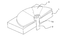
図1はこの発明の実施の形態1である半導体装置要部の構成を示す斜視図、図2は、図1の斜視断面図である。
1 is a perspective view showing a configuration of a main part of a semiconductor device according to
以下、図1、2に基づいて実施の形態1を説明する。
図1において、樹脂により封止された半導体素子で構成された半導体モジュール1には、その中央部に取付具としての取付ネジ部材である固定用ネジ2を貫通させるためのネジ貫通孔1aが設けられ、さらに、半導体モジュール1の表面すなわち上面には、押えばね部材である板状ばね3が重合され、その外周縁部が全周にわたり半導体モジュール1の上面に当接している。
この板状ばね3は、皿状(円錐形状)の弾性部材によって形成され、その中央頂部に半導体モジュール1のネジ貫通孔1aに対応してネジ貫通孔3aが設けられ、半導体モジュールの各辺より短小な直径の円錐形状のものである。
半導体モジュール1は、図6の従来例と同様に、ネジ貫通孔1aとネジ貫通孔3aを貫通してネジ孔7aにネジ込まれた固定用ネジ2の締結により、半導体モジュール1の下方に配設された固定部材(例えば冷却用放熱部材としての冷却装置。図6の7参照)に固定される。すなわち、この固定部材7(図6参照)に対する半導体モジュール1の固定は、固定ネジ頭部の、板状ばね3上面に加えられる圧力による弾性的な圧接で行われる。
上記のごとく、板状ばね3を半導体モジュールの各辺より短小な直径の円錐形状にしたので、板状ばね3の組み付け時に、板状ばね3が半導体モジュールの周辺より出っ張ることがなく、したがって回転方向の位置決めは何ら考慮する必要はなく、固定用ネジ2をネジ貫通孔1a、ネジ貫通孔3aに貫通させ締め付けを行えば組み付けは完了する。
The first embodiment will be described below with reference to FIGS.
In FIG. 1, a
The plate-
As in the conventional example of FIG. 6, the
As described above, since the
実施の形態2.
図3は、板状ばね3の反転現象を示す斜視断面図、図4は、この発明による実施の形態2における半導体装置要部の構成を示す斜視断面図である。
以下、図3、4に基づいて実施の形態2を説明する。
実施の形態1による組み付けの際、板状ばね3の特性である全圧縮時のばね反転現象によって、図3に示すようなばね反転の状態が発生するおそれがある。このような状態になると板状ばね本来の押え力が発生せずばね機能が満足できなくなる。そこで、この実施の形態2では、板状ばね3を全圧縮させず、すなわち反転現象を発生せしめず所定の力量を発生させるために、半導体モジュール1と板状ばね3の中央頂部間に、ばね反転防止用スぺ−サ4を介在させ、板状ばね3の全圧縮を回避しつつ所望の力量を得るようにしている。
このように構成したので、板状ばね3のばね反転状態の発生を防ぐことができる。
FIG. 3 is a perspective sectional view showing the inversion phenomenon of the
The second embodiment will be described below with reference to FIGS.
When assembled according to the first embodiment, a spring reversal state as shown in FIG. 3 may occur due to the spring reversal phenomenon during full compression, which is a characteristic of the
Since it comprised in this way, generation | occurrence | production of the spring reversal state of the plate-
実施の形態3.
図5は、この発明による実施の形態3における半導体装置要部の構成を示す斜視断面図である。
以下、図5に基づいて実施の形態3を説明する。
実施の形態2では、板状ばね3と反転防止用スぺ−サ4とは別々の部材で構成したが、実施の形態3は、この2者(板状ばね3と反転防止用スぺ−サ4)を図5に示すように一体成形し、一体部品5としたものである。
このように2者を一体部品5とすることにより作業性がさらに改善される。
FIG. 5 is a perspective sectional view showing the structure of the main part of the semiconductor device according to the third embodiment of the present invention.
The third embodiment will be described below with reference to FIG.
In the second embodiment, the
Thus, workability | operativity is further improved by making two persons into the integral component 5. FIG.
1 半導体モジュール 2 固定用ネジ
3 板状ばね 4 反転防止用スペーサ
5 板状ばね
1a、3a ネジ貫通孔 7 固定部材(放熱・冷却装置)。
DESCRIPTION OF
Claims (2)
Priority Applications (1)
| Application Number | Priority Date | Filing Date | Title |
|---|---|---|---|
| JP2007029297A JP4336718B2 (en) | 2007-02-08 | 2007-02-08 | Semiconductor device |
Applications Claiming Priority (1)
| Application Number | Priority Date | Filing Date | Title |
|---|---|---|---|
| JP2007029297A JP4336718B2 (en) | 2007-02-08 | 2007-02-08 | Semiconductor device |
Publications (2)
| Publication Number | Publication Date |
|---|---|
| JP2008198644A JP2008198644A (en) | 2008-08-28 |
| JP4336718B2 true JP4336718B2 (en) | 2009-09-30 |
Family
ID=39757351
Family Applications (1)
| Application Number | Title | Priority Date | Filing Date |
|---|---|---|---|
| JP2007029297A Active JP4336718B2 (en) | 2007-02-08 | 2007-02-08 | Semiconductor device |
Country Status (1)
| Country | Link |
|---|---|
| JP (1) | JP4336718B2 (en) |
Families Citing this family (6)
| Publication number | Priority date | Publication date | Assignee | Title |
|---|---|---|---|---|
| JP2011035265A (en) * | 2009-08-04 | 2011-02-17 | Mitsubishi Electric Corp | Semiconductor device |
| JP2013089711A (en) * | 2011-10-17 | 2013-05-13 | Mitsubishi Electric Corp | Semiconductor device |
| JP2014033119A (en) * | 2012-08-06 | 2014-02-20 | Mitsubishi Electric Corp | Semiconductor device |
| JP2013118423A (en) * | 2013-03-21 | 2013-06-13 | Mitsubishi Electric Corp | Semiconductor device |
| JP6065973B2 (en) | 2013-05-09 | 2017-01-25 | 三菱電機株式会社 | Semiconductor module |
| JP5754528B2 (en) * | 2014-03-19 | 2015-07-29 | 三菱電機株式会社 | Semiconductor device |
-
2007
- 2007-02-08 JP JP2007029297A patent/JP4336718B2/en active Active
Also Published As
| Publication number | Publication date |
|---|---|
| JP2008198644A (en) | 2008-08-28 |
Similar Documents
| Publication | Publication Date | Title |
|---|---|---|
| JP4336718B2 (en) | Semiconductor device | |
| JP5644706B2 (en) | Electronic component fixing structure for electric compressor | |
| JP5014016B2 (en) | Semiconductor device | |
| JP2007517407A (en) | Self-leveling heat sink system and method for multiple height devices | |
| JP2011035265A (en) | Semiconductor device | |
| US9633918B2 (en) | Semiconductor device | |
| JP3725103B2 (en) | Semiconductor device | |
| US6774468B2 (en) | Power semiconductor device | |
| JP4321459B2 (en) | Busbar mounting structure to heat dissipation plate | |
| JP6281432B2 (en) | Power converter | |
| JP5787435B2 (en) | Semiconductor heat dissipation device | |
| JP3914209B2 (en) | Semiconductor device | |
| JP5623463B2 (en) | Semiconductor module | |
| JP6800319B2 (en) | Power converter | |
| JP5988882B2 (en) | Semiconductor device | |
| JP2008258241A (en) | Semiconductor device | |
| JP7143096B2 (en) | circuit module | |
| JP4999060B2 (en) | Heat receiving member mounting structure | |
| JP2014033119A (en) | Semiconductor device | |
| JP5818944B1 (en) | Power converter | |
| TW200917944A (en) | Electronic apparatus and method of fixing cooling fan | |
| JP5974880B2 (en) | Semiconductor device and manufacturing method thereof | |
| JP5754528B2 (en) | Semiconductor device | |
| JP2013118423A (en) | Semiconductor device | |
| JP4336719B2 (en) | Semiconductor device |
Legal Events
| Date | Code | Title | Description |
|---|---|---|---|
| A977 | Report on retrieval |
Free format text: JAPANESE INTERMEDIATE CODE: A971007 Effective date: 20090501 |
|
| A131 | Notification of reasons for refusal |
Free format text: JAPANESE INTERMEDIATE CODE: A131 Effective date: 20090512 |
|
| A521 | Request for written amendment filed |
Free format text: JAPANESE INTERMEDIATE CODE: A523 Effective date: 20090603 |
|
| TRDD | Decision of grant or rejection written | ||
| A01 | Written decision to grant a patent or to grant a registration (utility model) |
Free format text: JAPANESE INTERMEDIATE CODE: A01 Effective date: 20090623 |
|
| A01 | Written decision to grant a patent or to grant a registration (utility model) |
Free format text: JAPANESE INTERMEDIATE CODE: A01 |
|
| A61 | First payment of annual fees (during grant procedure) |
Free format text: JAPANESE INTERMEDIATE CODE: A61 Effective date: 20090629 |
|
| FPAY | Renewal fee payment (event date is renewal date of database) |
Free format text: PAYMENT UNTIL: 20120703 Year of fee payment: 3 |
|
| R151 | Written notification of patent or utility model registration |
Ref document number: 4336718 Country of ref document: JP Free format text: JAPANESE INTERMEDIATE CODE: R151 |
|
| FPAY | Renewal fee payment (event date is renewal date of database) |
Free format text: PAYMENT UNTIL: 20120703 Year of fee payment: 3 |
|
| FPAY | Renewal fee payment (event date is renewal date of database) |
Free format text: PAYMENT UNTIL: 20120703 Year of fee payment: 3 |
|
| FPAY | Renewal fee payment (event date is renewal date of database) |
Free format text: PAYMENT UNTIL: 20130703 Year of fee payment: 4 |
|
| R250 | Receipt of annual fees |
Free format text: JAPANESE INTERMEDIATE CODE: R250 |
|
| R250 | Receipt of annual fees |
Free format text: JAPANESE INTERMEDIATE CODE: R250 |
|
| R250 | Receipt of annual fees |
Free format text: JAPANESE INTERMEDIATE CODE: R250 |
|
| R250 | Receipt of annual fees |
Free format text: JAPANESE INTERMEDIATE CODE: R250 |
|
| R250 | Receipt of annual fees |
Free format text: JAPANESE INTERMEDIATE CODE: R250 |
|
| R250 | Receipt of annual fees |
Free format text: JAPANESE INTERMEDIATE CODE: R250 |
|
| R250 | Receipt of annual fees |
Free format text: JAPANESE INTERMEDIATE CODE: R250 |
|
| R250 | Receipt of annual fees |
Free format text: JAPANESE INTERMEDIATE CODE: R250 |
|
| R250 | Receipt of annual fees |
Free format text: JAPANESE INTERMEDIATE CODE: R250 |
|
| R250 | Receipt of annual fees |
Free format text: JAPANESE INTERMEDIATE CODE: R250 |
|
| S111 | Request for change of ownership or part of ownership |
Free format text: JAPANESE INTERMEDIATE CODE: R313111 |
|
| R350 | Written notification of registration of transfer |
Free format text: JAPANESE INTERMEDIATE CODE: R350 |