JP5974880B2 - Semiconductor device and manufacturing method thereof - Google Patents
Semiconductor device and manufacturing method thereof Download PDFInfo
- Publication number
- JP5974880B2 JP5974880B2 JP2012271420A JP2012271420A JP5974880B2 JP 5974880 B2 JP5974880 B2 JP 5974880B2 JP 2012271420 A JP2012271420 A JP 2012271420A JP 2012271420 A JP2012271420 A JP 2012271420A JP 5974880 B2 JP5974880 B2 JP 5974880B2
- Authority
- JP
- Japan
- Prior art keywords
- extending
- extending portion
- cooling jacket
- base plate
- semiconductor device
- Prior art date
- Legal status (The legal status is an assumption and is not a legal conclusion. Google has not performed a legal analysis and makes no representation as to the accuracy of the status listed.)
- Expired - Fee Related
Links
Images


Description
本発明は、半導体モジュールを冷却ジャケットに取り付けた半導体装置及びその製造方法に関する。 The present invention relates to a semiconductor device in which a semiconductor module is attached to a cooling jacket and a manufacturing method thereof.
自動車や電車等のモータを制御するインバータや発電、回生用コンバータなどに、半導体素子と冷却フィンを樹脂で封止したトランスファーモールド型の半導体モジュールが用いられる。この半導体モジュールを冷却ジャケットに取り付ける際に、従来は半導体モジュールの樹脂封止部から延びるベース板の四隅を冷却ジャケットにネジ止めしていた(例えば、特許文献1参照)。 A transfer mold type semiconductor module in which a semiconductor element and a cooling fin are sealed with a resin is used for an inverter for controlling a motor of an automobile, a train or the like, a power generation, a regeneration converter, or the like. When this semiconductor module is attached to the cooling jacket, conventionally, the four corners of the base plate extending from the resin sealing portion of the semiconductor module are screwed to the cooling jacket (for example, see Patent Document 1).
しかし、ベース板にネジ穴を設けるスペースが必要になるため、半導体モジュールのサイズが大きくなる。このため、製造装置と搬送装置が大型化するという問題があった。 However, since a space for providing screw holes in the base plate is required, the size of the semiconductor module increases. For this reason, there existed a problem that a manufacturing apparatus and a conveying apparatus enlarged.
本発明は、上述のような課題を解決するためになされたもので、その目的は半導体モジュールを縮小して製造装置と搬送装置の大型化を防ぐことができる半導体装置及びその製造方法を得るものである。 The present invention has been made to solve the above-described problems, and an object of the present invention is to obtain a semiconductor device capable of reducing the size of a semiconductor module and preventing an increase in size of a manufacturing apparatus and a transport apparatus and a manufacturing method thereof. It is.
本発明に係る半導体装置の製造方法は、冷却フィンのベース板の実装部上に半導体素子を実装し、前記半導体素子と前記実装部を樹脂で封止して半導体モジュールを形成する工程と、前記実装部から横方向に延びる前記ベース板の第1の延設部を冷却ジャケットの固定部の差込口に差し込む工程と、前記第1の延設部を前記差込口に差し込んだ状態で、前記実装部から前記第1の延設部とは反対方向に延びる前記ベース板の第2の延設部を前記冷却ジャケットに固定して、前記半導体モジュールを前記冷却ジャケットに取り付ける工程とを備え、前記固定部において、前記第1の延設部が差し込まれる部分の下方に溝を設けることを特徴とする。
The method of manufacturing a semiconductor device according to the present invention includes a step of mounting a semiconductor element on a mounting portion of a base plate of a cooling fin, and sealing the semiconductor element and the mounting portion with a resin to form a semiconductor module; A step of inserting the first extending portion of the base plate extending in the lateral direction from the mounting portion into the insertion port of the fixing portion of the cooling jacket; and the state in which the first extending portion is inserted into the insertion port, Fixing the second extending portion of the base plate extending from the mounting portion in a direction opposite to the first extending portion to the cooling jacket, and attaching the semiconductor module to the cooling jacket , In the fixing portion, a groove is provided below a portion into which the first extending portion is inserted .
本発明により、半導体モジュールを縮小して製造装置と搬送装置の大型化を防ぐことができる。 According to the present invention, it is possible to reduce the size of a semiconductor module and prevent an increase in size of a manufacturing apparatus and a transfer apparatus.
本発明の実施の形態に係る半導体装置及びその製造方法について図面を参照して説明する。同じ又は対応する構成要素には同じ符号を付し、説明の繰り返しを省略する場合がある。 A semiconductor device and a manufacturing method thereof according to an embodiment of the present invention will be described with reference to the drawings. The same or corresponding components are denoted by the same reference numerals, and repeated description may be omitted.
実施の形態1.
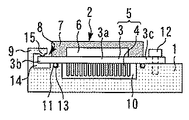
図1は、本発明の実施の形態1に係る半導体装置を示す上面図である。図2は図1のI−IIに沿った断面図である。冷却ジャケット1にトランスファーモールド型の半導体モジュール2が取り付けられている。
FIG. 1 is a top view showing a semiconductor device according to
半導体モジュール2は、ベース板3とその下方に設けられた複数のフィン4を含む冷却フィン5と、ベース板3の実装部3a上に実装された半導体素子6と、半導体素子6と実装部3aを封止する樹脂7とを有する。ベース板3は、実装部3aと、実装部3aから横方向に延びる延設部3bと、実装部3aから延設部3bとは反対方向に延びる延設部3cとを有する。延設部3b,3cは半導体モジュール2の四角形状の樹脂7の四隅から反対方向に延びている。
The
冷却ジャケット1の上面には、差込口8を持つ固定部9と、冷却水路10と、Oリング用溝11とが設けられている。ベース板3の延設部3bが固定部9の差込口8に差し込まれている。ベース板3の延設部3cが冷却ジャケット1にネジ12によりネジ止めされて固定されている。複数のフィン4は冷却ジャケット1の冷却水路10に収納されている。水漏れを防ぐためOリング用溝11内にOリング13が用いられている。
On the upper surface of the
続いて、本実施の形態の製造方法を説明する。まず、冷却フィン5のベース板3の実装部3a上に半導体素子6を実装し、半導体素子6と実装部3aを樹脂7で封止して半導体モジュール2を形成する。
Then, the manufacturing method of this Embodiment is demonstrated. First, the
次に、実装部3aから横方向に延びるベース板3の延設部3bを冷却ジャケット1の固定部9の差込口8に差し込む。次に、延設部3bを差込口8に差し込んだ状態で、実装部3aから延設部3cとは反対方向に延びるベース板3の延設部3cを冷却ジャケット1にネジ止めして固定して、半導体モジュール2を冷却ジャケット1に取り付ける。
Next, the extending
本実施の形態では、冷却フィン5のベース板3の延設部3bを冷却ジャケット1の固定部9の差込口8に差し込むことにより、延設部3bを冷却ジャケット1にネジ止めする場合に比べて延設部3bの長さを短くすることができる。この結果、半導体モジュール2を縮小できるため、製造装置と搬送装置の大型化を防ぐことができる。また、延設部3bのネジ止めを無くすことで部品点数を削減できる。
In the present embodiment, when the extending
実施の形態2.
図3は、本発明の実施の形態2に係る半導体装置を示す断面図である。実施の形態1の構成に加えて、固定部9において、延設部3bが差し込まれる部分の下方に溝14が設けられている。
FIG. 3 is a sectional view showing a semiconductor device according to the second embodiment of the present invention. In addition to the configuration of the first embodiment, a
この溝14により延設部3bを固定部9に斜めに深く差し込むことができるため、差し込み時に冷却フィン5と冷却ジャケット1の接触を防ぐことができる。この結果、冷却フィン5の面積を増やして冷却性能を向上させることができる。
Since the extended
実施の形態3.
図4は、本発明の実施の形態3に係る半導体装置を示す断面図である。実施の形態1の構成に加えて、固定部9の延設部3bとの接触面に突起15が設けられている。この突起15が延設部3bを押さえ付けている。組み立て時において、延設部3bを差込口8に差し込む際に延設部3bと突起15が接触しないようにする。そして、延設部3cをネジ止めする際に突起15で延設部3bを押さえ付ける。これにより、冷却フィン5のベース板3と冷却ジャケット1の密着性を向上させることができる。
FIG. 4 is a cross-sectional view showing a semiconductor device according to
なお、上記の機能を生じるように突起15の高さを調整する必要がある。突起の断面形状はベース板3に食い込みやすい三角形状が好ましいが、半円状、四角形状でもよい。
In addition, it is necessary to adjust the height of the
実施の形態4.
図5は、本発明の実施の形態4に係る半導体装置を示す上面図である。図6は図5のI−IIに沿った断面図である。実施の形態1とは異なり、半導体モジュール2のベース板3の延設部3b,3cにネジ穴が設けられていない。そして、半導体モジュール2が冷却ジャケット1に外付け部品16により取り付けられている。具体的には、ベース板3の延設部3b,3cが外付け部品16により冷却ジャケット1に押し付けられてネジ止めされて固定されている。外付け部品16はネジ12により冷却ジャケット1に固定されている。外付け部品16の断面形状はS字状である。
FIG. 5 is a top view showing a semiconductor device according to the fourth embodiment of the present invention. 6 is a cross-sectional view taken along line I-II in FIG. Unlike the first embodiment, the extending
ベース板3の延設部3b,3cを直接ネジ止めするのではなく外付け部品16で固定するため、延設部3b,3cにネジ穴を設ける必要が無い。従って、延設部3b,3cの長さを短くすることができる。この結果、半導体モジュール2を縮小できるため、製造装置と搬送装置の大型化を防ぐことができる。また、延設部3bのネジ止めを無くすことで部品点数を削減できる。
Since the extending
図7は、本発明の実施の形態4に係る半導体装置の変形例を示す断面図である。この例では外付け部品16の断面形状は長方形状である。ベース板3の延設部3b,3cを冷却ジャケット1に押し付けて固定できるものであれば、外付け部品16の断面形状はS字状に限らず、長方形状や正方形状でもよい。
FIG. 7 is a sectional view showing a modification of the semiconductor device according to the fourth embodiment of the present invention. In this example, the cross-sectional shape of the
なお、半導体素子6は、珪素によって形成されたものに限らず、珪素に比べてバンドギャップが大きいワイドバンドギャップ半導体によって形成されたものでもよい。ワイドバンドギャップ半導体は、例えば、炭化珪素、窒化ガリウム系材料、又はダイヤモンドである。このようなワイドバンドギャップ半導体によって形成された半導体素子6は、耐電圧性や許容電流密度が高いため、小型化できる。この小型化された素子を用いることで、この素子を組み込んだ半導体モジュール2も小型化できる。また、素子の耐熱性が高いため、冷却フィン5を小型化でき、冷却部を空冷化できるので、半導体装置を更に小型化できる。また、素子の電力損失が低く高効率であるため、半導体モジュール2を高効率化できる。
The
1 冷却ジャケット、2 半導体モジュール、3 ベース板、3a 実装部、3b,3c 延設部、5 冷却フィン、6 半導体素子、7 樹脂、8 差込口、9 固定部、14 溝、15 突起、16 外付け部品
DESCRIPTION OF
Claims (6)
前記実装部から横方向に延びる前記ベース板の第1の延設部を冷却ジャケットの固定部の差込口に差し込む工程と、
前記第1の延設部を前記差込口に差し込んだ状態で、前記実装部から前記第1の延設部とは反対方向に延びる前記ベース板の第2の延設部を前記冷却ジャケットに固定して、前記半導体モジュールを前記冷却ジャケットに取り付ける工程とを備え、
前記固定部において、前記第1の延設部が差し込まれる部分の下方に溝を設けることを特徴とする半導体装置の製造方法。 Mounting a semiconductor element on the mounting portion of the base plate of the cooling fin, and sealing the semiconductor element and the mounting portion with a resin to form a semiconductor module;
Inserting the first extending portion of the base plate extending laterally from the mounting portion into the insertion port of the fixing portion of the cooling jacket;
With the first extending portion inserted into the insertion port, the second extending portion of the base plate extending from the mounting portion in the direction opposite to the first extending portion is used as the cooling jacket. Fixing and attaching the semiconductor module to the cooling jacket ,
In the fixing portion, a groove is provided below a portion into which the first extending portion is inserted .
前記第1の延設部を前記差込口に差し込む際に前記第1の延設部と前記突起が接触しないようにし、
前記第2の延設部を固定する際に前記突起で前記第1の延設部を押さえ付けることを特徴とする請求項1又は2に記載の半導体装置の製造方法。 Protrusions are provided on the contact surface of the fixed portion with the first extending portion,
When the first extending portion is inserted into the insertion port, the first extending portion and the protrusion are not in contact with each other,
3. The method of manufacturing a semiconductor device according to claim 1, wherein the first extending portion is pressed by the protrusion when the second extending portion is fixed. 4.
前記冷却ジャケットに取り付けられた半導体モジュールとを備え、
前記半導体モジュールは、ベース板を含む冷却フィンと、前記ベース板の実装部上に実装された半導体素子と、前記半導体素子と前記実装部を封止する樹脂とを有し、
前記冷却ジャケットは、差込口を持つ固定部を有し、
前記実装部から横方向に延びる前記ベース板の第1の延設部が前記固定部の前記差込口に差し込まれ、
前記実装部から前記第1の延設部とは反対方向に延びる前記ベース板の第2の延設部が前記冷却ジャケットに固定され、
前記固定部において、前記第1の延設部が差し込まれる部分の下方に溝が設けられていることを特徴とする半導体装置。 A cooling jacket,
A semiconductor module attached to the cooling jacket,
The semiconductor module includes a cooling fin including a base plate, a semiconductor element mounted on a mounting portion of the base plate, and a resin that seals the semiconductor element and the mounting portion.
The cooling jacket has a fixing part having an insertion port,
A first extending portion of the base plate extending laterally from the mounting portion is inserted into the insertion port of the fixing portion;
A second extending portion of the base plate extending from the mounting portion in a direction opposite to the first extending portion is fixed to the cooling jacket ;
The semiconductor device according to claim 1, wherein a groove is provided below the portion into which the first extending portion is inserted in the fixing portion .
前記突起が前記第1の延設部を押さえ付けていることを特徴とする請求項4又は5に記載の半導体装置。 A protrusion is provided on a contact surface of the fixed portion with the first extending portion,
6. The semiconductor device according to claim 4, wherein the protrusion presses the first extending portion.
Priority Applications (1)
| Application Number | Priority Date | Filing Date | Title |
|---|---|---|---|
| JP2012271420A JP5974880B2 (en) | 2012-12-12 | 2012-12-12 | Semiconductor device and manufacturing method thereof |
Applications Claiming Priority (1)
| Application Number | Priority Date | Filing Date | Title |
|---|---|---|---|
| JP2012271420A JP5974880B2 (en) | 2012-12-12 | 2012-12-12 | Semiconductor device and manufacturing method thereof |
Publications (3)
| Publication Number | Publication Date |
|---|---|
| JP2014116546A JP2014116546A (en) | 2014-06-26 |
| JP2014116546A5 JP2014116546A5 (en) | 2015-01-15 |
| JP5974880B2 true JP5974880B2 (en) | 2016-08-23 |
Family
ID=51172229
Family Applications (1)
| Application Number | Title | Priority Date | Filing Date |
|---|---|---|---|
| JP2012271420A Expired - Fee Related JP5974880B2 (en) | 2012-12-12 | 2012-12-12 | Semiconductor device and manufacturing method thereof |
Country Status (1)
| Country | Link |
|---|---|
| JP (1) | JP5974880B2 (en) |
Families Citing this family (1)
| Publication number | Priority date | Publication date | Assignee | Title |
|---|---|---|---|---|
| CN107426940B (en) * | 2016-05-24 | 2019-04-30 | 上汽通用五菱汽车股份有限公司 | A kind of automobile-used DC/DC converter heat dissipating method |
Family Cites Families (6)
| Publication number | Priority date | Publication date | Assignee | Title |
|---|---|---|---|---|
| JPS56154054U (en) * | 1980-04-14 | 1981-11-18 | ||
| JP2000082774A (en) * | 1998-06-30 | 2000-03-21 | Sumitomo Electric Ind Ltd | Power module and substrate therefor |
| JP3864282B2 (en) * | 1998-09-22 | 2006-12-27 | 三菱マテリアル株式会社 | Power module substrate, method for manufacturing the same, and semiconductor device using the substrate |
| JP4396366B2 (en) * | 2004-04-08 | 2010-01-13 | 日産自動車株式会社 | Semiconductor device |
| JP2005302882A (en) * | 2004-04-08 | 2005-10-27 | Nissan Motor Co Ltd | Semiconductor device |
| JP2008270295A (en) * | 2007-04-16 | 2008-11-06 | Sumitomo Electric Ind Ltd | Semiconductor device |
-
2012
- 2012-12-12 JP JP2012271420A patent/JP5974880B2/en not_active Expired - Fee Related
Also Published As
| Publication number | Publication date |
|---|---|
| JP2014116546A (en) | 2014-06-26 |
Similar Documents
| Publication | Publication Date | Title |
|---|---|---|
| JP4760585B2 (en) | Power semiconductor device | |
| JP5875467B2 (en) | Power semiconductor device | |
| JP5432085B2 (en) | Power semiconductor device | |
| US20150021750A1 (en) | Semiconductor device and method for manufacturing the same | |
| JP2015073012A (en) | Semiconductor device | |
| CN108292631B (en) | Semiconductor module | |
| JP6391527B2 (en) | Power semiconductor module | |
| JP6286541B2 (en) | Power module device and power conversion device | |
| JP5974880B2 (en) | Semiconductor device and manufacturing method thereof | |
| JP2016092209A (en) | Power semiconductor device, and method of manufacturing the same | |
| JP6480098B2 (en) | Semiconductor device | |
| JP2008198644A (en) | Semiconductor device | |
| JP2007252177A (en) | Power converter | |
| US9357678B2 (en) | Semiconductor module | |
| CN110637362B (en) | Semiconductor package | |
| JP2015126207A (en) | Semiconductor device | |
| US9355999B2 (en) | Semiconductor device | |
| JP2008028311A (en) | Semiconductor device | |
| JP2007173301A (en) | Dissipator for cooling semiconductor element, semiconductor device, and manufacturing process of dissipator for cooling semiconductor element | |
| US20160351469A1 (en) | Semiconductor device | |
| US20170120719A1 (en) | Power heat dissipation device | |
| JP5669657B2 (en) | Semiconductor device | |
| JP2017022209A (en) | Semiconductor module | |
| JP5700092B2 (en) | Semiconductor device | |
| JP6108802B2 (en) | Heat dissipation structure |
Legal Events
| Date | Code | Title | Description |
|---|---|---|---|
| A621 | Written request for application examination |
Free format text: JAPANESE INTERMEDIATE CODE: A621 Effective date: 20141110 |
|
| A521 | Written amendment |
Free format text: JAPANESE INTERMEDIATE CODE: A523 Effective date: 20141119 |
|
| A977 | Report on retrieval |
Free format text: JAPANESE INTERMEDIATE CODE: A971007 Effective date: 20151217 |
|
| A131 | Notification of reasons for refusal |
Free format text: JAPANESE INTERMEDIATE CODE: A131 Effective date: 20160126 |
|
| A521 | Written amendment |
Free format text: JAPANESE INTERMEDIATE CODE: A523 Effective date: 20160301 |
|
| TRDD | Decision of grant or rejection written | ||
| A01 | Written decision to grant a patent or to grant a registration (utility model) |
Free format text: JAPANESE INTERMEDIATE CODE: A01 Effective date: 20160621 |
|
| A61 | First payment of annual fees (during grant procedure) |
Free format text: JAPANESE INTERMEDIATE CODE: A61 Effective date: 20160704 |
|
| R150 | Certificate of patent or registration of utility model |
Ref document number: 5974880 Country of ref document: JP Free format text: JAPANESE INTERMEDIATE CODE: R150 |
|
| LAPS | Cancellation because of no payment of annual fees |