JP4311340B2 - Constant current drive - Google Patents
Constant current drive Download PDFInfo
- Publication number
- JP4311340B2 JP4311340B2 JP2004326794A JP2004326794A JP4311340B2 JP 4311340 B2 JP4311340 B2 JP 4311340B2 JP 2004326794 A JP2004326794 A JP 2004326794A JP 2004326794 A JP2004326794 A JP 2004326794A JP 4311340 B2 JP4311340 B2 JP 4311340B2
- Authority
- JP
- Japan
- Prior art keywords
- current
- current mirror
- constant current
- field effect
- mirror
- Prior art date
- Legal status (The legal status is an assumption and is not a legal conclusion. Google has not performed a legal analysis and makes no representation as to the accuracy of the status listed.)
- Expired - Fee Related
Links
- 239000003990 capacitor Substances 0.000 claims description 10
- 230000005669 field effect Effects 0.000 description 73
- 239000011159 matrix material Substances 0.000 description 9
- 238000010586 diagram Methods 0.000 description 6
- 238000006243 chemical reaction Methods 0.000 description 3
- 238000005401 electroluminescence Methods 0.000 description 1
Images


Classifications
-
- G—PHYSICS
- G05—CONTROLLING; REGULATING
- G05F—SYSTEMS FOR REGULATING ELECTRIC OR MAGNETIC VARIABLES
- G05F3/00—Non-retroactive systems for regulating electric variables by using an uncontrolled element, or an uncontrolled combination of elements, such element or such combination having self-regulating properties
- G05F3/02—Regulating voltage or current
- G05F3/08—Regulating voltage or current wherein the variable is dc
- G05F3/10—Regulating voltage or current wherein the variable is dc using uncontrolled devices with non-linear characteristics
- G05F3/16—Regulating voltage or current wherein the variable is dc using uncontrolled devices with non-linear characteristics being semiconductor devices
- G05F3/20—Regulating voltage or current wherein the variable is dc using uncontrolled devices with non-linear characteristics being semiconductor devices using diode- transistor combinations
- G05F3/26—Current mirrors
- G05F3/262—Current mirrors using field-effect transistors only
-
- G—PHYSICS
- G09—EDUCATION; CRYPTOGRAPHY; DISPLAY; ADVERTISING; SEALS
- G09G—ARRANGEMENTS OR CIRCUITS FOR CONTROL OF INDICATING DEVICES USING STATIC MEANS TO PRESENT VARIABLE INFORMATION
- G09G3/00—Control arrangements or circuits, of interest only in connection with visual indicators other than cathode-ray tubes
- G09G3/20—Control arrangements or circuits, of interest only in connection with visual indicators other than cathode-ray tubes for presentation of an assembly of a number of characters, e.g. a page, by composing the assembly by combination of individual elements arranged in a matrix no fixed position being assigned to or needed to be assigned to the individual characters or partial characters
- G09G3/22—Control arrangements or circuits, of interest only in connection with visual indicators other than cathode-ray tubes for presentation of an assembly of a number of characters, e.g. a page, by composing the assembly by combination of individual elements arranged in a matrix no fixed position being assigned to or needed to be assigned to the individual characters or partial characters using controlled light sources
- G09G3/30—Control arrangements or circuits, of interest only in connection with visual indicators other than cathode-ray tubes for presentation of an assembly of a number of characters, e.g. a page, by composing the assembly by combination of individual elements arranged in a matrix no fixed position being assigned to or needed to be assigned to the individual characters or partial characters using controlled light sources using electroluminescent panels
- G09G3/32—Control arrangements or circuits, of interest only in connection with visual indicators other than cathode-ray tubes for presentation of an assembly of a number of characters, e.g. a page, by composing the assembly by combination of individual elements arranged in a matrix no fixed position being assigned to or needed to be assigned to the individual characters or partial characters using controlled light sources using electroluminescent panels semiconductive, e.g. using light-emitting diodes [LED]
- G09G3/3208—Control arrangements or circuits, of interest only in connection with visual indicators other than cathode-ray tubes for presentation of an assembly of a number of characters, e.g. a page, by composing the assembly by combination of individual elements arranged in a matrix no fixed position being assigned to or needed to be assigned to the individual characters or partial characters using controlled light sources using electroluminescent panels semiconductive, e.g. using light-emitting diodes [LED] organic, e.g. using organic light-emitting diodes [OLED]
- G09G3/3275—Details of drivers for data electrodes
- G09G3/3283—Details of drivers for data electrodes in which the data driver supplies a variable data current for setting the current through, or the voltage across, the light-emitting elements
-
- G—PHYSICS
- G09—EDUCATION; CRYPTOGRAPHY; DISPLAY; ADVERTISING; SEALS
- G09G—ARRANGEMENTS OR CIRCUITS FOR CONTROL OF INDICATING DEVICES USING STATIC MEANS TO PRESENT VARIABLE INFORMATION
- G09G3/00—Control arrangements or circuits, of interest only in connection with visual indicators other than cathode-ray tubes
- G09G3/20—Control arrangements or circuits, of interest only in connection with visual indicators other than cathode-ray tubes for presentation of an assembly of a number of characters, e.g. a page, by composing the assembly by combination of individual elements arranged in a matrix no fixed position being assigned to or needed to be assigned to the individual characters or partial characters
- G09G3/22—Control arrangements or circuits, of interest only in connection with visual indicators other than cathode-ray tubes for presentation of an assembly of a number of characters, e.g. a page, by composing the assembly by combination of individual elements arranged in a matrix no fixed position being assigned to or needed to be assigned to the individual characters or partial characters using controlled light sources
- G09G3/30—Control arrangements or circuits, of interest only in connection with visual indicators other than cathode-ray tubes for presentation of an assembly of a number of characters, e.g. a page, by composing the assembly by combination of individual elements arranged in a matrix no fixed position being assigned to or needed to be assigned to the individual characters or partial characters using controlled light sources using electroluminescent panels
- G09G3/32—Control arrangements or circuits, of interest only in connection with visual indicators other than cathode-ray tubes for presentation of an assembly of a number of characters, e.g. a page, by composing the assembly by combination of individual elements arranged in a matrix no fixed position being assigned to or needed to be assigned to the individual characters or partial characters using controlled light sources using electroluminescent panels semiconductive, e.g. using light-emitting diodes [LED]
- G09G3/3208—Control arrangements or circuits, of interest only in connection with visual indicators other than cathode-ray tubes for presentation of an assembly of a number of characters, e.g. a page, by composing the assembly by combination of individual elements arranged in a matrix no fixed position being assigned to or needed to be assigned to the individual characters or partial characters using controlled light sources using electroluminescent panels semiconductive, e.g. using light-emitting diodes [LED] organic, e.g. using organic light-emitting diodes [OLED]
- G09G3/3216—Control arrangements or circuits, of interest only in connection with visual indicators other than cathode-ray tubes for presentation of an assembly of a number of characters, e.g. a page, by composing the assembly by combination of individual elements arranged in a matrix no fixed position being assigned to or needed to be assigned to the individual characters or partial characters using controlled light sources using electroluminescent panels semiconductive, e.g. using light-emitting diodes [LED] organic, e.g. using organic light-emitting diodes [OLED] using a passive matrix
Description
本発明は有機エレクトロルミネセンス素子(以下有機EL素子と称する)や発光ダイオード(以下LEDと称する)等の電流駆動素子をマトリックス状に配置した表示装置を駆動するのに適用して好適な定電流駆動装置に関する。 The present invention is a constant current suitable for driving a display device in which current drive elements such as organic electroluminescence elements (hereinafter referred to as organic EL elements) and light emitting diodes (hereinafter referred to as LEDs) are arranged in a matrix. The present invention relates to a driving device.
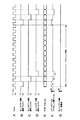
従来、有機EL素子やLED等の電流駆動素子1を図4に示す如くマトリックス状に配置した表示装置が提案されている。図4例は説明を簡単にするためこの電流駆動素子1をマトリックス状に3×3個としたものが記載されているが、実際にはマトリックス状に例えば500×500個の画像表示装置が実現されている。
Conventionally, a display device has been proposed in which
図4に示す如き、電流駆動素子1をマトリックス状に配置した表示装置を駆動するのに線順次駆動が行なわれている。この場合、この電流駆動素子1の駆動源には一般的に電流源2a,2b,2cが用いられている。
As shown in FIG. 4, line-sequential driving is performed to drive a display device in which
この図4に示す如き、電流駆動素子1をマトリックス状に配置した表示装置において、画像を表示するのには、接続スイッチ3a,3b,3cで横のラインを順次選択し、縦の各ラインに画像の輝度に応じた電流を流せば良い。この場合、線順次であるので縦の各ラインの電流は、横のラインと同期して一斉に流す必要がある。
In the display device in which the
この画像の輝度に応じた電流を流すのに、電流源2a,2b,2cを夫々定電流とし、画像の輝度に応じたパルス幅変調信号(PWM(Pulse Width Modulation))により接続スイッチ4a,4b,4cをオン・オフする。即ち、画像の輝度に応じて接続スイッチ4a,4b,4cを横のラインが接続スイッチ3a,3b,3cにより選ばれている時間内でオン−オフすれば良い。明るくしたいときには、オン時間を長く、暗くしたいときにはオン時間を短くする。
In order to flow the current according to the brightness of the image, the
従来、この電流源2a,2b,2cに使用される定電流回路として図5に示す如きものが提案されている。この図5につき説明するに、5は定電流発生部を構成する演算増幅回路を示し、この演算増幅回路5の非反転入力端子+を定電流Iの値を決定するリファレンス電圧Vrefを得る電池6を介して接地し、この演算増幅回路5の反転入力端子−を抵抗器7を介して接地する。
Conventionally, a constant current circuit as shown in FIG. 5 has been proposed as a constant current circuit used for the
また、この演算増幅回路5の出力端子をn形の電界効果トランジスタ8のゲートに接続し、この電界効果トランジスタ8のソースを演算増幅回路5の反転入力端子−に接続し、この電界効果トランジスタ8のドレインをカレントミラー回路のリファレンス側を構成するダイオード接続したp形の電界効果トランジスタ9のドレインとゲートとの接続点に接続し、この電界効果トランジスタ9のソースを正の直流電圧が供給される電源端子10に接続する。
The output terminal of the
この電界効果トランジスタ9のゲートをカレントミラー回路のミラー側を構成するp形の電界効果トランジスタ11のゲートに接続し、この電界効果トランジスタ11のソースを電源端子10に接続し、この電界効果トランジスタ11のドレインを例えば接続スイッチ4aに接続する如くする。
The gate of the field effect transistor 9 is connected to the gate of a p-type
この定電流発生部の電界効果トランジスタ8のドレイン−ソース間に流れる電流Iは
I=Vref÷R
となり一定の電流値となる。ここで、Vrefは電池6によるリファレンス電圧、Rは抵抗器7の抵抗値である。
The current I flowing between the drain and the source of the
And a constant current value. Here, Vref is a reference voltage by the battery 6, and R is a resistance value of the resistor 7.
この定電流Iは、電界効果トランジスタ9から供給され、この電界効果トランジスタ9とカレントミラー回路を構成するミラー側の電界効果トランジスタ11にもこの定電流Iが流れ、この定電流Iが例えば接続スイッチ4aを介して表示装置を構成する電流駆動素子1に供給される。
The constant current I is supplied from the field effect transistor 9, and the constant current I flows also to the
斯る図5に示す如き定電流回路を図4に示す如き表示装置の電流源2a,2b,2cとして使用したときには、この図5に示す如き定電流回路を例えば500個も必要とし回路規模が大きくなると共に消費電力が大きくなる不都合がある。
When such a constant current circuit as shown in FIG. 5 is used as the
そこで定電流発生部の演算増幅回路5、電池6及び抵抗器7を全カレントミラー回路に共通とするようにした図6に示す如き電流駆動素子1をマトリックス状に配した定電流駆動装置が提案されている。この図6につき説明するにこの図6において、図5に対応する部分には同一符号を付して、その詳細説明は省略する。
Therefore, a constant current driving device is proposed in which the
この図6においては定電流発生部を構成する演算増幅回路5の非反転入力端子+を定電流Iの値を決定するリファレンス電圧Vrefを得る電池6を介して接地し、この演算増幅回路5の反転入力端子−を抵抗器7を介して接地する。
In FIG. 6, the non-inverting input terminal + of the
また、この演算増幅回路5の出力端子を全カレントミラー回路に応じた数、例えば500個、図6では3個のn形の電界効果トランジスタ8a,8b及び8cの夫々のゲートに接続し、この電界効果トランジスタ8a,8b及び8cの夫々のソースを演算増幅回路5の反転入力端子−に接続する。
Further, the output terminals of the
また、この電界効果トランジスタ8a,8b及び8cの夫々のドレインを夫々カレントミラー回路のリファレンス側を構成するダイオード接続したp形の電界効果トランジスタ9a,9b及び9cの夫々のゲートとドレインとの接続点に接続し、この電界効果トランジスタ9a,9b及び9cの夫々のソースを正の直流電圧が供給される電源端子10に接続する。
Also, the connection points of the gates and drains of the p-type
この電界効果トランジスタ9a,9b及び9cの夫々のゲートを夫々カレントミラー回路のミラー側を構成するp形の電界効果トランジスタ11a,11b及び11cの夫々のゲートに夫々接続し、この電界効果トランジスタ11a,11b及び11cの夫々のソースを電源端子10に接続し、この電界効果トランジスタ11a,11b及び11cの夫々のドレインを夫々例えば接続スイッチ4a,4b及び4cに接続する如くする。
The gates of the
この定電流発生部の電界効果トランジスタ8a,8b及び8cの夫々のドレイン−ソース間に流れる電流Iは
I=Vref÷nR (nは並列に接続されるカレントミラーの数)
となり一定の電流値となる。
The current I flowing between the drain and source of each of the
And a constant current value.
この定電流Iは、夫々電界効果トランジスタ9a,9b及び9cから夫々供給され、この電界効果トランジスタ9a,9b及び9cと夫々カレントミラー回路を構成するミラー側の夫々の電界効果トランジスタ11a,11b及び11cにも、この定電流Iが流れ、この定電流Iが例えば接続スイッチ4a,4b及び4cを介して表示装置を構成する電流駆動素子1に供給される。
The constant current I is supplied from
従来、電流駆動素子をマトリックス状に配した表示装置の定電流駆動装置として特許文献1に開示されたものも提案されている。
然しながら、図6に示す如き、電界効果トランジスタ8a,8b,8c,9a,9b,9c,11a,11b,11cには特性のバラツキがあり、この電界効果トランジスタの特性のバラツキにより夫々の定電流Iの値にバラツキを生じる不都合があると共に複数例えば500個のカレントミラー回路においては、常にリファレンス側とミラー側とに同じ電流が流れるので消費電力が大となる不都合がある。
However, as shown in FIG. 6, the
本発明は、斯る点に鑑み、電界効果トランジスタに特性のバラツキがあっても定電流Iの値にバラツキがないようにすると共に消費電力を改善することを目的とする。 In view of this point, an object of the present invention is to prevent variations in the value of the constant current I even when there are variations in characteristics of field effect transistors, and to improve power consumption.
上記課題を解決するため、本発明の定電流駆動装置は、リファレンス側及びミラー側より成る複数のカレントミラー回路と、複数のカレントミラー回路の夫々のリファレンス側に一定の電流を発生させる定電流発生部と、複数のカレントミラー回路の夫々のリファレンス側とミラー側の駆動信号入力部と接続する電流保持用容量素子と、複数のカレントミラー回路の夫々のリファレンス側及びミラー側を電気的に接続する第1のスイッチ手段と、第1のスイッチ手段と連動し、定電流発生部を複数のカレントミラー回路のリファレンス側に接続する第2のスイッチ手段と、複数のカレントミラー回路を一定の周期で順次選択して、選択中のカレントミラー回路に係る第1のスイッチ手段及び第2のスイッチ手段をオンにする順次選択手段と、複数のカレントミラー回路ごとに、各カレントミラー回路のミラー側の特性のバラツキに対応した補正値が予め記憶されている記憶手段と、順次選択手段による複数のカレントミラー回路の選択の周期に合わせて、選択中のカレントミラー回路のミラー側の特性に対応する補正値を記憶手段から読み出し、定電流発生部が発生させる電流を補正値に基づいて切り換えさせる選択・読み出し手段とを備えるものである。
カレントミラー回路の選択が変更されるたびに、補正値が、選択しているカレントミラー回路のミラー側の特性のバラツキに対応した補正値に変更され、選択しているカレントミラー回路のリファレンス側に当該補正値に応じた一定の電流が発生する。 In order to solve the above-described problems, a constant current driving device according to the present invention includes a plurality of current mirror circuits composed of a reference side and a mirror side, and constant current generation for generating a constant current on each reference side of the plurality of current mirror circuits. and parts, and the current holding capacitive element connected to the reference side of each the mirror side of the drive signal input section of the plurality of current mirror circuits to electrically connect the reference side and the mirror side of each of the plurality of current mirror circuits The first switch means, the second switch means for connecting the constant current generator to the reference side of the plurality of current mirror circuits in conjunction with the first switch means, and the plurality of current mirror circuits sequentially in a constant cycle select, and sequentially selects unit to turn on the first switch means and second switch means in accordance with the current mirror circuit in the selection, For each of the current mirror circuits, correction values corresponding to variations in characteristics on the mirror side of each current mirror circuit are stored in advance, and in accordance with the selection cycle of a plurality of current mirror circuits by the sequential selection means. And a selection / reading means for reading a correction value corresponding to the mirror-side characteristic of the current mirror circuit being selected from the storage means, and for switching the current generated by the constant current generator based on the correction value .
Each time the selection of the current mirror circuit is changed, the correction value is changed to a correction value corresponding to the variation in characteristics on the mirror side of the selected current mirror circuit, and is changed to the reference side of the selected current mirror circuit. A constant current corresponding to the correction value is generated.
本発明によれば、複数のカレントミラー回路の選択の周期と同期して、各カレントミラー回路のリファレンス側に発生する電流を補正値に基づき変更(補正)することにより、当該各カレントミラー回路のミラー側を流れる電流の大きさを一定することができる。そのため、例えば各カレントミラー回路を構成する電界効果トランジスタの特性にバラツキがあっても、各カレントミラー回路のミラー側を流れる定電流の値のバラツキをなくすことができる。 According to the present invention, the current generated on the reference side of each current mirror circuit is changed (corrected) on the basis of the correction value in synchronization with the selection cycle of the plurality of current mirror circuits. The magnitude of the current flowing on the mirror side can be made constant. Therefore, for example, even if there are variations in the characteristics of the field effect transistors constituting the respective current mirror circuits, it is possible to eliminate variations in the value of constant-current flowing through the mirror side of the current mirror circuit.
また本発明によれば、複数のカレントミラー回路のうちの選択されたカレントミラー回路以外のカレントミラー回路は電流保持用容量によりミラー側にのみ定電流Iを流すようにしているので、消費電力が略々半分に改善される。 Further, according to the present invention, the current mirror circuit other than the selected current mirror circuit among the plurality of current mirror circuits is configured to cause the constant current I to flow only to the mirror side by the current holding capacitor. It is improved by about half.
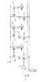
以下、図1、図2及び図3を参照して本発明定電流駆動装置を実施するための最良の形態の例につき説明する。この図1、図2において、図6に対応する部分には同一符号を付して示す。 Hereinafter, an example of the best mode for carrying out the constant current driving device of the present invention will be described with reference to FIG. 1, FIG. 2 and FIG. In FIG. 1 and FIG. 2, parts corresponding to those in FIG.
本例においては、図1に示す如く、定電流発生部を構成する演算増幅回路5の反転入力端子−を抵抗器7を介して接地する。この演算増幅回路5の出力端子をn形の電界効果トランジスタ8のゲートに接続し、この電界効果トランジスタ8のソースを演算増幅回路5の反転入力端子−に接続する。
In this example, as shown in FIG. 1, the inverting input terminal − of the
また、本例においては、この定電流発生部を構成する電界効果トランジスタ8のドレインを夫々接続スイッチを構成するp形の電界効果トランジスタ20a,20b及び20cの夫々のドレインに接続し、この接続スイッチを構成する電界効果トランジスタ20a,20b及び20cの夫々のソースを夫々カレントミラー回路のリファレンス側を構成するp形の電界効果トランジスタ9a,9b及び9cの夫々のドレインに接続し、この電界効果トランジスタ9a,9b及び9cの夫々のソースを正の直流電圧が供給される電源端子10に接続する。
In this example, the drain of the
この電界効果トランジスタ9a,9b及び9cの夫々のゲートを夫々カレントミラー回路のミラー側を構成するp形の電界効果トランジスタ11a,11b及び11cの夫々のゲートに夫々接続し、この電界効果トランジスタ11a,11b及び11cの夫々のソースを電源端子10に接続し、この電界効果トランジスタ11a,11b及び11cの夫々のドレインを夫々例えば接続スイッチ4a,4b及び4cに接続する如くする。
The gates of the
本例においては、電界効果トランジスタ9a,9b及び9cの夫々のゲートと電界効果トランジスタ11a,11b及び11cの夫々のゲートとの夫々の接続点を夫々ミラー側の電界効果トランジスタ11a,11b及び11cの電流を保持するためのゲート電圧を保持する電流保持用容量21a,21b及び21cを介して電源端子10に接続する。
In this example, the connection points between the respective gates of the
また本例においては、電界効果トランジスタ9a,9b及び9cの夫々のドレインを夫々接続スイッチを構成するp形の電界効果トランジスタ22a,22b及び22cの夫々のドレインに接続し、この電界効果トランジスタ22a,22b及び22cの夫々のソースを電界効果トランジスタ9a,9b及び9cの夫々のゲートに夫々接続する。
In this example, the drains of the
また、図1において、23はマイクロコンピュータ等より構成されたカレントミラー回路を順次選択すると共に予め設定されたリファレンス電圧を順次読み出すカレントミラー回路選択及びリファレンス電圧読み出し回路を示し、このカレントミラー回路選択及びリファレンス電圧読み出し回路23が発生する図3Aに示す如きクロック信号をシフトレジスタ24a,24b,24cに供給すると共にこのクロック信号に同期して選択パルスを図3B,C及びDに示す如く順次、シフトレジスタ24a,24b及び24cに供給し、このシフトレジスタ24a,24b及び24cを所定周期毎に選択する如くする。
In FIG. 1,
このシフトレジスタ24aを接続スイッチを構成する電界効果トランジスタ20a及び22aの夫々のゲートに接続し、このシフトレジスタ24aに選択パルスが供給されたときに、この電界効果トランジスタ20a及び22aがオンとなる如くし、またシフトレジスタ24bを接続スイッチを構成する電界効果トランジスタ20b及び22bの夫々のゲートに接続し、このシフトレジスタ24bに選択パルスが供給されたときに、この電界効果トランジスタ20b及び22bがオンとなる如くし、またシフトレジスタ24cを接続スイッチを構成する電界効果トランジスタ20c及び22cの夫々のゲートに接続し、このシフトレジスタ24cに選択パルスが供給されたときに、この電界効果トランジスタ20c及び22cがオンとなる如くする。
The
従って、接続スイッチを構成する電界効果トランジスタ20a及び22aと20b及び22bと20c及び22cとがクロック信号により順次シフトする選択パルスにより順次オンされるので、同時にオンすることはない。
Accordingly, the
例えば、選択パルスがシフトレジスタ24aに供給されたときは図2に示す如く、電界効果トランジスタ20a及び22aがオンし、電界効果トランジスタ20b及び22bと20c及び22cとはオフしている状態である。
For example, when the selection pulse is supplied to the
図1において、25は、この複数のカレントミラー回路の夫々のミラー側の電界効果トランジスタ11a,11b及び11cに流れる定電流Iの値が図3Gに示す如く一定になる様に、夫々のカレントミラー回路を構成する電界効果トランジスタの特性のバラツキに対応し、予め演算増幅回路5の非反転入力端子+に供給する図3Fに示す如きリファレンス電圧Va,Vb,Vcを夫々測定して、所定アドレスに記憶したROM等より成る記憶装置を示す。
In FIG. 1,
この記憶装置25は、カレントミラー回路選択及びリファレンス電圧読み出し回路23よりのカレントミラー回路のミラー側の電界効果トランジスタに一定の定電流Iを流す予め定めたリファレンス電圧を図3Eに示す如き読み出しアドレスで読み出す如くする。
This
この記憶装置25より読み出されたデジタルのリファレンス電圧をデジタル−アナログ変換回路26に供給し、このデジタル−アナログ変換回路26の出力側に得られる図3Fに示す如きリファレンス電圧Va,Vb,Vcをカレントミラー回路の選択に同期して演算増幅回路5の非反転入力端子+に供給する如くする。
The digital reference voltage read from the
本例は上述の如く構成されているので、例えば第1番目のシフトレジスタ24aが選択パルスにより選択されたときは、図2に示す如く接続スイッチを構成する電界効果トランジスタ20a及び22aがオンし、接続スイッチを構成する電界効果トランジスタ20b及び22bと20c及び22cとはオフ状態である。
Since this example is configured as described above, for example, when the
この接続スイッチを構成する電界効果トランジスタ20a及び22aがオンしているカレントミラー回路はリファレンス側の電界効果トランジスタ9aが定電流発生部の電界効果トランジスタ8に接続され、ミラー側の電界効果トランジスタ11aに定電流Iが流れる。
In the current mirror circuit in which the
この場合、本例においては、カレントミラー回路選択及びリファレンス電圧読み出し回路よりの読み出し信号により、記憶装置25から第1番目のカレントミラー回路のリファレンス電圧Vaが読み出され、このリファレンス電圧Vaが演算増幅回路5の非反転入力端子+に供給され、電界効果トランジスタ9a及び11aの特性のバラツキを考慮して定電流Iが流れる。
In this case, in this example, the reference voltage Va of the first current mirror circuit is read from the
このときは、電流保持用容量21aに電流が流れ、この電流保持用容量21aにミラー側の電界効果トランジスタ11aに定電流を流し続けるためのゲート電圧を保持する電荷が充電される。
At this time, a current flows through the
第2及び第3番目のシフトレジスタ24b及び24cが選択パルスにより選択されたときも上述同様に動作する。
The same operation as described above is performed when the second and
この接続スイッチを構成する電界効果トランジスタ20b及び22bと20c及び22cとがオフとなっているカレントミラー回路はリファレンス側の電界効果トランジスタ9b,9cの電流は「0」である。ミラー側の電界効果トランジスタ11b,11cの電流は一番最初だけ「0」であるが、選択パルスにより選択された後は、電流保持用容量21b,21cに保持された電荷により定電流Iを流し続けることができる。
In the current mirror circuit in which the
一方、電流保持用容量21a,21b,21cに蓄積した電荷は時間が経過すると放電するので適当な周期で充電する必要があるが、接続スイッチを構成する電界効果トランジスタ20a及び22aと20b及び22bと20c及び22cとが周期的にオンすることで解決している。
On the other hand, since the electric charges accumulated in the
また、第2番目及び第3番目のシフトレジスタ24b及び24cが選択パルスにより選択されたときは、カレントミラー回路選択及びリファレンス電圧読み出し回路23よりの読み出し信号により記憶装置25に記憶した第2及び第3番目のカレントミラー回路の電界効果トランジスタ9b,11b及び9c,11cの特性のバラツキを考慮した一定の定電流Iを流すリファレンス電圧Vb及びVcを読み出し、これを演算増幅回路5の非反転入力端子+に供給しているので、ミラー側の電界効果トランジスタ11b及び11cに一定の定電流Iを流すことができる。
Further, when the second and
本例によれば、複数のカレントミラー回路の選択の周期に合わせてミラー側電界効果トランジスタ11a,11b,11cの電流が一定になるように定電流発生部のリファレンス電圧Va,Vb,Vcを切り換えるようにしているので電界効果トランジスタの特性にバラツキがあっても定電流Iの値のバラツキをなくすことができる。
According to this example, the reference voltages Va, Vb, and Vc of the constant current generator are switched so that the currents of the mirror-side
また本例によれば、複数のカレントミラー回路のうちの選択されたカレントミラー回路以外のカレントミラー回路は電流保持用容量21a,21b,21cによりミラー側の電界効果トランジスタ11a,11b,11cにのみ定電流Iを流すようにしているので、消費電力が略々半分に改善される。
Further, according to the present example, the current mirror circuits other than the selected current mirror circuit among the plurality of current mirror circuits are only connected to the
尚、上述例は、電界効果トランジスタを使用してカレントミラー回路を構成した例につき述べたが、この電界効果トランジスタの代わりにトランジスタを使用しても良いことは勿論である。 In the above example, the current mirror circuit is configured by using a field effect transistor. However, it goes without saying that a transistor may be used instead of the field effect transistor.
また、本発明は上述例に限ることなく、本発明の要旨を逸脱することなく、その他種々の構成が採り得ることは勿論である。 Further, the present invention is not limited to the above-described example, and various other configurations can be adopted without departing from the gist of the present invention.
5‥‥演算増幅回路、7‥‥抵抗器、8,9a,9b,9c,11a,11b,11c,20a,20b,20c,22a,22b,22c‥‥電界効果トランジスタ、10‥‥電源端子、21a,21b,21c‥‥電流保持用容量、23‥‥カレントミラー回路選択及びリファレンス電圧読み出し回路、24a,24b,24c‥‥シフトレジスタ、25‥‥記憶装置、26‥‥デジタル−アナログ変換回路 5... Operational amplifier circuit, 7... Resistor, 8, 9a, 9b, 9c, 11a, 11b, 11c, 20a, 20b, 20c, 22a, 22b, 22c .. field effect transistor, 10. 21a, 21b, 21c ... current holding capacity, 23 ... current mirror circuit selection and reference voltage readout circuit, 24a, 24b, 24c ... shift register, 25 ... storage device, 26 ... digital-analog conversion circuit
Claims (3)
前記複数のカレントミラー回路の夫々のリファレンス側に一定の電流を発生させる定電流発生部と、
前記複数のカレントミラー回路の夫々のリファレンス側とミラー側の駆動信号入力部と接続する電流保持用容量素子と、
前記複数のカレントミラー回路の夫々のリファレンス側及びミラー側を電気的に接続する第1のスイッチ手段と、
前記第1のスイッチ手段と連動し、前記定電流発生部を前記複数のカレントミラー回路のリファレンス側に接続する第2のスイッチ手段と、
前記複数のカレントミラー回路を一定の周期で順次選択して、選択中のカレントミラー回路に係る前記第1のスイッチ手段及び前記第2のスイッチ手段をオンにする順次選択手段と、
前記複数のカレントミラー回路ごとに、各カレントミラー回路のミラー側の特性のバラツキに対応した補正値が予め記憶されている記憶手段と、
前記順次選択手段による前記複数のカレントミラー回路の選択の周期に合わせて、前記選択中のカレントミラー回路のミラー側の特性に対応する補正値を前記記憶手段から読み出し、前記定電流発生部が発生させる電流を前記補正値に基づいて切り換えさせる選択・読み出し手段と
を備える定電流駆動装置。 A plurality of current mirror circuits composed of a reference side and a mirror side;
A constant current generator for generating a constant current on each reference side of the plurality of current mirror circuits;
A current holding capacitive element connected to a reference signal side and a mirror side drive signal input unit of each of the plurality of current mirror circuits;
First switch means for electrically connecting a reference side and a mirror side of each of the plurality of current mirror circuits;
In conjunction with the first switch means, second switch means for connecting said constant current generation unit to the reference side of the front Symbol plurality of current mirror circuits,
Sequential selection means for sequentially selecting the plurality of current mirror circuits at a constant period and turning on the first switch means and the second switch means according to the current mirror circuit being selected;
Storage means for storing correction values corresponding to variations in characteristics on the mirror side of each current mirror circuit in advance for each of the plurality of current mirror circuits;
In accordance with the selection cycle of the plurality of current mirror circuits by the sequential selection means, a correction value corresponding to the mirror-side characteristic of the current mirror circuit being selected is read from the storage means, and the constant current generator generates Selection / reading means for switching the current to be switched based on the correction value;
A constant current drive device comprising:
前記第1のスイッチ手段及び前記第2のスイッチ手段がオンのとき、前記複数のカレントミラー回路のうち、前記順次選択手段により選択されたカレントミラー回路のリファレンス側及びミラー側に前記電流保持用容量素子から駆動信号を供給するとともに当該電流保持用容量素子に充電を行い、
前記第1のスイッチ手段及び前記第2のスイッチ手段がオフのとき、選択されていない夫々のカレントミラー回路のミラー側に対してのみ前記電流保持用容量素子から駆動信号を供給する
定電流駆動装置。 The constant current drive device according to claim 1,
When the first switch means and the second switch means are on, the current holding capacitors are provided on the reference side and the mirror side of the current mirror circuit selected by the sequential selection means among the plurality of current mirror circuits. Supply a drive signal from the element and charge the current holding capacitor element,
A constant current drive device for supplying a drive signal from the current holding capacitor element only to the mirror side of each of the unselected current mirror circuits when the first switch means and the second switch means are OFF .
前記選択・読み出し手段は、所定周波数のクロック信号及び前記複数のカレントミラー回路から該当カレントミラー回路を選択するための選択信号を発生し、The selection / reading unit generates a selection signal for selecting a current mirror circuit from a clock signal having a predetermined frequency and the plurality of current mirror circuits,
前記順次選択手段は、前記クロック信号の周波数で前記選択信号に基づいてカレントミラー回路を選択するThe sequential selection means selects a current mirror circuit based on the selection signal at the frequency of the clock signal.
定電流駆動装置。Constant current drive device.
Priority Applications (7)
| Application Number | Priority Date | Filing Date | Title |
|---|---|---|---|
| JP2004326794A JP4311340B2 (en) | 2004-11-10 | 2004-11-10 | Constant current drive |
| TW094138251A TW200636654A (en) | 2004-11-10 | 2005-11-01 | Constant-current drive |
| EP05806605A EP1811358B1 (en) | 2004-11-10 | 2005-11-09 | Constant current driving device |
| DE602005024292T DE602005024292D1 (en) | 2004-11-10 | 2005-11-09 | CONSTANT CURRENT DRIVER |
| PCT/JP2005/020978 WO2006051992A1 (en) | 2004-11-10 | 2005-11-09 | Constant current driving device |
| KR1020067013364A KR101127494B1 (en) | 2004-11-10 | 2005-11-09 | Constant current driving device |
| US10/585,338 US7808284B2 (en) | 2004-11-10 | 2005-11-09 | Constant current drive device |
Applications Claiming Priority (1)
| Application Number | Priority Date | Filing Date | Title |
|---|---|---|---|
| JP2004326794A JP4311340B2 (en) | 2004-11-10 | 2004-11-10 | Constant current drive |
Publications (2)
| Publication Number | Publication Date |
|---|---|
| JP2006139405A JP2006139405A (en) | 2006-06-01 |
| JP4311340B2 true JP4311340B2 (en) | 2009-08-12 |
Family
ID=36336657
Family Applications (1)
| Application Number | Title | Priority Date | Filing Date |
|---|---|---|---|
| JP2004326794A Expired - Fee Related JP4311340B2 (en) | 2004-11-10 | 2004-11-10 | Constant current drive |
Country Status (7)
| Country | Link |
|---|---|
| US (1) | US7808284B2 (en) |
| EP (1) | EP1811358B1 (en) |
| JP (1) | JP4311340B2 (en) |
| KR (1) | KR101127494B1 (en) |
| DE (1) | DE602005024292D1 (en) |
| TW (1) | TW200636654A (en) |
| WO (1) | WO2006051992A1 (en) |
Families Citing this family (10)
| Publication number | Priority date | Publication date | Assignee | Title |
|---|---|---|---|---|
| JP4809030B2 (en) * | 2005-09-28 | 2011-11-02 | 株式会社リコー | DRIVE CIRCUIT AND ELECTRONIC DEVICE USING THE DRIVE CIRCUIT |
| CN101878498A (en) * | 2007-09-12 | 2010-11-03 | 康宁股份有限公司 | In wide dynamic range, produce the method and apparatus of accurate electric current |
| JP4565283B2 (en) | 2008-06-10 | 2010-10-20 | マイクロン テクノロジー, インク. | Voltage adjustment system |
| US8183892B2 (en) | 2009-06-05 | 2012-05-22 | Fairchild Semiconductor Corporation | Monolithic low impedance dual gate current sense MOSFET |
| US8816600B2 (en) | 2011-05-13 | 2014-08-26 | Nxp B.V. | Method of power and temperature control for high brightness light emitting diodes |
| CN102722213B (en) * | 2012-06-26 | 2014-03-26 | 昆明物理研究所 | Photovoltaic detector read-out unit circuit applying inverted voltage follower |
| CN103632635B (en) * | 2013-11-08 | 2016-04-13 | 电子科技大学 | Power tube grouping hybrid driving circuit |
| CN104485073B (en) * | 2014-12-25 | 2017-02-22 | 广东威创视讯科技股份有限公司 | Brightness adjustment method and system for LED display screens |
| US20180348805A1 (en) * | 2017-05-31 | 2018-12-06 | Silicon Laboratories Inc. | Bias Current Generator |
| US10720098B2 (en) * | 2017-11-15 | 2020-07-21 | Facebook Technologies, Llc | Pulse-width-modulation control of micro LED |
Family Cites Families (15)
| Publication number | Priority date | Publication date | Assignee | Title |
|---|---|---|---|---|
| JPS62121492A (en) * | 1985-11-22 | 1987-06-02 | 日立超エル・エス・アイエンジニアリング株式会社 | Display module |
| JPH0219909A (en) * | 1988-07-08 | 1990-01-23 | Canon Inc | Constant current circuit |
| US5963071A (en) * | 1998-01-22 | 1999-10-05 | Nanoamp Solutions, Inc. | Frequency doubler with adjustable duty cycle |
| JP3315652B2 (en) * | 1998-09-07 | 2002-08-19 | キヤノン株式会社 | Current output circuit |
| KR100296113B1 (en) * | 1999-06-03 | 2001-07-12 | 구본준, 론 위라하디락사 | ElectroLuminescent Display |
| KR100566813B1 (en) * | 2000-02-03 | 2006-04-03 | 엘지.필립스 엘시디 주식회사 | Circuit for Electro Luminescence Cell |
| KR100327374B1 (en) * | 2000-03-06 | 2002-03-06 | 구자홍 | an active driving circuit for a display panel |
| JP3610923B2 (en) * | 2001-05-30 | 2005-01-19 | ソニー株式会社 | Active matrix display device, active matrix organic electroluminescence display device, and driving method thereof |
| CN101257743B (en) * | 2001-08-29 | 2011-05-25 | 株式会社半导体能源研究所 | Light emitting device, method of driving a light emitting device |
| JP2003187988A (en) * | 2001-12-20 | 2003-07-04 | Sharp Corp | Driving device of white light-emitting diode |
| KR100618574B1 (en) * | 2001-12-29 | 2006-08-31 | 엘지.필립스 엘시디 주식회사 | Drive circuit organic electro luminescent display |
| JP2003273749A (en) * | 2002-03-18 | 2003-09-26 | Seiko Epson Corp | Signal transmission device and method thereof, and electronic device and appliance |
| JP3866606B2 (en) * | 2002-04-08 | 2007-01-10 | Necエレクトロニクス株式会社 | Display device drive circuit and drive method thereof |
| US7271784B2 (en) * | 2002-12-18 | 2007-09-18 | Semiconductor Energy Laboratory Co., Ltd. | Display device and driving method thereof |
| JP4662698B2 (en) * | 2003-06-25 | 2011-03-30 | ルネサスエレクトロニクス株式会社 | Current source circuit and current setting method |
-
2004
- 2004-11-10 JP JP2004326794A patent/JP4311340B2/en not_active Expired - Fee Related
-
2005
- 2005-11-01 TW TW094138251A patent/TW200636654A/en not_active IP Right Cessation
- 2005-11-09 WO PCT/JP2005/020978 patent/WO2006051992A1/en active Application Filing
- 2005-11-09 EP EP05806605A patent/EP1811358B1/en not_active Expired - Fee Related
- 2005-11-09 KR KR1020067013364A patent/KR101127494B1/en not_active IP Right Cessation
- 2005-11-09 DE DE602005024292T patent/DE602005024292D1/en active Active
- 2005-11-09 US US10/585,338 patent/US7808284B2/en not_active Expired - Fee Related
Also Published As
| Publication number | Publication date |
|---|---|
| EP1811358A4 (en) | 2009-01-21 |
| KR20070085046A (en) | 2007-08-27 |
| DE602005024292D1 (en) | 2010-12-02 |
| US7808284B2 (en) | 2010-10-05 |
| WO2006051992A1 (en) | 2006-05-18 |
| US20090121750A1 (en) | 2009-05-14 |
| EP1811358A1 (en) | 2007-07-25 |
| TWI309402B (en) | 2009-05-01 |
| JP2006139405A (en) | 2006-06-01 |
| EP1811358B1 (en) | 2010-10-20 |
| KR101127494B1 (en) | 2012-03-23 |
| TW200636654A (en) | 2006-10-16 |
Similar Documents
| Publication | Publication Date | Title |
|---|---|---|
| US7808284B2 (en) | Constant current drive device | |
| US9424770B2 (en) | Error compensator and organic light emitting display device using the same | |
| US8749454B2 (en) | Image display device and method of controlling the same | |
| TWI358706B (en) | Image display apparatus | |
| US7453383B2 (en) | Digital-to-analog converting circuit, electrooptical device, and electronic apparatus | |
| JP5184625B2 (en) | Display panel device and control method thereof | |
| JP2004191752A5 (en) | ||
| KR20100124338A (en) | Oled display panel with pwm control | |
| JP2007256344A (en) | Power circuit, lcd driver ic, lcd driver circuit, and liquid crystal display device | |
| JP2007060732A (en) | Display | |
| JP2005077864A5 (en) | ||
| JPH10260664A (en) | Liquid crystal driving circuit and liquid crystal device using the same | |
| JP2011048101A (en) | Pixel circuit and display device | |
| KR101788218B1 (en) | DC-DC Converter and Mobile Communication Terminal using The Same | |
| JP2005156859A (en) | Driving device and driving method of self-luminous display panel | |
| JP4493359B2 (en) | Self-luminous display module and driving method thereof | |
| TWI252462B (en) | Image display apparatus having gradation potential generating circuit | |
| JP4487488B2 (en) | Display device drive circuit, mobile phone, and portable electronic device | |
| TWI253616B (en) | Active matrix type display apparatus | |
| JP4759908B2 (en) | Flat display device | |
| JP3705116B2 (en) | Power supply device | |
| JP2004361643A (en) | Driving device for light emitting display panel | |
| JP2007114308A (en) | Driving unit and driving method for light emitting display panel | |
| JP5381823B2 (en) | Pixel driving device, light emitting device, electronic device, and driving control method for light emitting device | |
| JP2008233703A (en) | Liquid crystal display |
Legal Events
| Date | Code | Title | Description |
|---|---|---|---|
| A131 | Notification of reasons for refusal |
Free format text: JAPANESE INTERMEDIATE CODE: A131 Effective date: 20081224 |
|
| A521 | Request for written amendment filed |
Free format text: JAPANESE INTERMEDIATE CODE: A523 Effective date: 20090223 |
|
| TRDD | Decision of grant or rejection written | ||
| A01 | Written decision to grant a patent or to grant a registration (utility model) |
Free format text: JAPANESE INTERMEDIATE CODE: A01 Effective date: 20090421 |
|
| A01 | Written decision to grant a patent or to grant a registration (utility model) |
Free format text: JAPANESE INTERMEDIATE CODE: A01 |
|
| A61 | First payment of annual fees (during grant procedure) |
Free format text: JAPANESE INTERMEDIATE CODE: A61 Effective date: 20090504 |
|
| FPAY | Renewal fee payment (event date is renewal date of database) |
Free format text: PAYMENT UNTIL: 20120522 Year of fee payment: 3 |
|
| FPAY | Renewal fee payment (event date is renewal date of database) |
Free format text: PAYMENT UNTIL: 20120522 Year of fee payment: 3 |
|
| FPAY | Renewal fee payment (event date is renewal date of database) |
Free format text: PAYMENT UNTIL: 20120522 Year of fee payment: 3 |
|
| FPAY | Renewal fee payment (event date is renewal date of database) |
Free format text: PAYMENT UNTIL: 20130522 Year of fee payment: 4 |
|
| LAPS | Cancellation because of no payment of annual fees |