JP4292575B2 - Piezoelectric device and method of manufacturing lid - Google Patents
Piezoelectric device and method of manufacturing lid Download PDFInfo
- Publication number
- JP4292575B2 JP4292575B2 JP2003388131A JP2003388131A JP4292575B2 JP 4292575 B2 JP4292575 B2 JP 4292575B2 JP 2003388131 A JP2003388131 A JP 2003388131A JP 2003388131 A JP2003388131 A JP 2003388131A JP 4292575 B2 JP4292575 B2 JP 4292575B2
- Authority
- JP
- Japan
- Prior art keywords
- lid
- glass
- metal substrate
- package
- hole
- Prior art date
- Legal status (The legal status is an assumption and is not a legal conclusion. Google has not performed a legal analysis and makes no representation as to the accuracy of the status listed.)
- Expired - Fee Related
Links
- 238000004519 manufacturing process Methods 0.000 title claims description 19
- 239000011521 glass Substances 0.000 claims description 117
- 229910052751 metal Inorganic materials 0.000 claims description 83
- 239000002184 metal Substances 0.000 claims description 83
- 239000000758 substrate Substances 0.000 claims description 77
- 239000000463 material Substances 0.000 claims description 45
- 238000005260 corrosion Methods 0.000 claims description 19
- 230000007797 corrosion Effects 0.000 claims description 19
- 238000010438 heat treatment Methods 0.000 claims description 18
- 238000000034 method Methods 0.000 claims description 17
- 239000006060 molten glass Substances 0.000 claims description 17
- 238000007789 sealing Methods 0.000 claims description 14
- 230000002093 peripheral effect Effects 0.000 claims description 11
- 238000002844 melting Methods 0.000 claims description 9
- 230000008018 melting Effects 0.000 claims description 9
- 238000001039 wet etching Methods 0.000 claims description 9
- 238000005520 cutting process Methods 0.000 claims description 8
- 230000001678 irradiating effect Effects 0.000 claims description 5
- 238000001704 evaporation Methods 0.000 claims description 3
- 239000007769 metal material Substances 0.000 claims description 2
- PXHVJJICTQNCMI-UHFFFAOYSA-N Nickel Chemical compound [Ni] PXHVJJICTQNCMI-UHFFFAOYSA-N 0.000 description 10
- 238000005530 etching Methods 0.000 description 10
- 239000010931 gold Substances 0.000 description 8
- 230000000694 effects Effects 0.000 description 7
- 230000005284 excitation Effects 0.000 description 7
- 229910000833 kovar Inorganic materials 0.000 description 7
- 239000000853 adhesive Substances 0.000 description 6
- 230000001070 adhesive effect Effects 0.000 description 6
- PCHJSUWPFVWCPO-UHFFFAOYSA-N gold Chemical compound [Au] PCHJSUWPFVWCPO-UHFFFAOYSA-N 0.000 description 6
- 229910052737 gold Inorganic materials 0.000 description 6
- 238000001465 metallisation Methods 0.000 description 6
- 238000012545 processing Methods 0.000 description 6
- 230000008569 process Effects 0.000 description 5
- WFKWXMTUELFFGS-UHFFFAOYSA-N tungsten Chemical compound [W] WFKWXMTUELFFGS-UHFFFAOYSA-N 0.000 description 5
- 229910052721 tungsten Inorganic materials 0.000 description 5
- 239000010937 tungsten Substances 0.000 description 5
- 230000005540 biological transmission Effects 0.000 description 4
- 239000011651 chromium Substances 0.000 description 4
- 238000001312 dry etching Methods 0.000 description 4
- 238000005304 joining Methods 0.000 description 4
- 229910052759 nickel Inorganic materials 0.000 description 4
- 239000010453 quartz Substances 0.000 description 4
- VYPSYNLAJGMNEJ-UHFFFAOYSA-N silicon dioxide Inorganic materials O=[Si]=O VYPSYNLAJGMNEJ-UHFFFAOYSA-N 0.000 description 4
- 239000013078 crystal Substances 0.000 description 3
- 238000003780 insertion Methods 0.000 description 3
- 230000037431 insertion Effects 0.000 description 3
- 230000004048 modification Effects 0.000 description 3
- 238000012986 modification Methods 0.000 description 3
- 230000035515 penetration Effects 0.000 description 3
- 238000007747 plating Methods 0.000 description 3
- VYZAMTAEIAYCRO-UHFFFAOYSA-N Chromium Chemical compound [Cr] VYZAMTAEIAYCRO-UHFFFAOYSA-N 0.000 description 2
- 229910000640 Fe alloy Inorganic materials 0.000 description 2
- 235000014676 Phragmites communis Nutrition 0.000 description 2
- 229910001128 Sn alloy Inorganic materials 0.000 description 2
- 239000011230 binding agent Substances 0.000 description 2
- 239000005388 borosilicate glass Substances 0.000 description 2
- 239000000919 ceramic Substances 0.000 description 2
- 229910052804 chromium Inorganic materials 0.000 description 2
- 230000007423 decrease Effects 0.000 description 2
- 238000010586 diagram Methods 0.000 description 2
- 230000005684 electric field Effects 0.000 description 2
- 238000000605 extraction Methods 0.000 description 2
- 238000010304 firing Methods 0.000 description 2
- JVPLOXQKFGYFMN-UHFFFAOYSA-N gold tin Chemical compound [Sn].[Au] JVPLOXQKFGYFMN-UHFFFAOYSA-N 0.000 description 2
- 229910052736 halogen Inorganic materials 0.000 description 2
- 150000002367 halogens Chemical class 0.000 description 2
- 238000010030 laminating Methods 0.000 description 2
- 238000000465 moulding Methods 0.000 description 2
- 239000002245 particle Substances 0.000 description 2
- 238000007517 polishing process Methods 0.000 description 2
- 230000009467 reduction Effects 0.000 description 2
- 239000003566 sealing material Substances 0.000 description 2
- 238000003466 welding Methods 0.000 description 2
- WSMQKESQZFQMFW-UHFFFAOYSA-N 5-methyl-pyrazole-3-carboxylic acid Chemical compound CC1=CC(C(O)=O)=NN1 WSMQKESQZFQMFW-UHFFFAOYSA-N 0.000 description 1
- 229910000531 Co alloy Inorganic materials 0.000 description 1
- 101001139126 Homo sapiens Krueppel-like factor 6 Proteins 0.000 description 1
- 229910021578 Iron(III) chloride Inorganic materials 0.000 description 1
- 229910001030 Iron–nickel alloy Inorganic materials 0.000 description 1
- 229910000990 Ni alloy Inorganic materials 0.000 description 1
- BQCADISMDOOEFD-UHFFFAOYSA-N Silver Chemical compound [Ag] BQCADISMDOOEFD-UHFFFAOYSA-N 0.000 description 1
- 230000002411 adverse Effects 0.000 description 1
- 229910045601 alloy Inorganic materials 0.000 description 1
- 239000000956 alloy Substances 0.000 description 1
- 238000013459 approach Methods 0.000 description 1
- 238000005452 bending Methods 0.000 description 1
- 230000015572 biosynthetic process Effects 0.000 description 1
- 238000005219 brazing Methods 0.000 description 1
- 230000008859 change Effects 0.000 description 1
- 239000010941 cobalt Substances 0.000 description 1
- GUTLYIVDDKVIGB-UHFFFAOYSA-N cobalt atom Chemical compound [Co] GUTLYIVDDKVIGB-UHFFFAOYSA-N 0.000 description 1
- 238000007872 degassing Methods 0.000 description 1
- 238000000151 deposition Methods 0.000 description 1
- 238000009713 electroplating Methods 0.000 description 1
- 230000007613 environmental effect Effects 0.000 description 1
- 230000006870 function Effects 0.000 description 1
- 230000009931 harmful effect Effects 0.000 description 1
- 230000001771 impaired effect Effects 0.000 description 1
- 238000007689 inspection Methods 0.000 description 1
- 239000011810 insulating material Substances 0.000 description 1
- RBTARNINKXHZNM-UHFFFAOYSA-K iron trichloride Chemical compound Cl[Fe](Cl)Cl RBTARNINKXHZNM-UHFFFAOYSA-K 0.000 description 1
- GQYHUHYESMUTHG-UHFFFAOYSA-N lithium niobate Chemical compound [Li+].[O-][Nb](=O)=O GQYHUHYESMUTHG-UHFFFAOYSA-N 0.000 description 1
- 238000010295 mobile communication Methods 0.000 description 1
- 239000011224 oxide ceramic Substances 0.000 description 1
- 229910052574 oxide ceramic Inorganic materials 0.000 description 1
- TWNQGVIAIRXVLR-UHFFFAOYSA-N oxo(oxoalumanyloxy)alumane Chemical compound O=[Al]O[Al]=O TWNQGVIAIRXVLR-UHFFFAOYSA-N 0.000 description 1
- 229920002120 photoresistant polymer Polymers 0.000 description 1
- 238000005498 polishing Methods 0.000 description 1
- 239000000843 powder Substances 0.000 description 1
- 230000004044 response Effects 0.000 description 1
- 238000007788 roughening Methods 0.000 description 1
- 239000004065 semiconductor Substances 0.000 description 1
- 238000000926 separation method Methods 0.000 description 1
- 229910052709 silver Inorganic materials 0.000 description 1
- 239000004332 silver Substances 0.000 description 1
- 238000005245 sintering Methods 0.000 description 1
- 238000004544 sputter deposition Methods 0.000 description 1
- 238000000992 sputter etching Methods 0.000 description 1
- 238000003860 storage Methods 0.000 description 1
- 230000003746 surface roughness Effects 0.000 description 1
- 229920003002 synthetic resin Polymers 0.000 description 1
- 239000000057 synthetic resin Substances 0.000 description 1
Images


Landscapes
- Piezo-Electric Or Mechanical Vibrators, Or Delay Or Filter Circuits (AREA)
Description
本発明は、パッケージ内に圧電振動片を収容した圧電デバイスと蓋体の製造方法に関する。 The present invention relates to a piezoelectric device in which a piezoelectric vibrating piece is accommodated in a package and a method for manufacturing a lid.
HDD(ハード・ディスク・ドライブ)、モバイルコンピュータ、あるいはICカード等の小型の情報機器や、携帯電話、自動車電話、またはページングシステム等の移動体通信機器やジャイロセンサ等において、圧電振動子や圧電発振器等の圧電デバイスが広く使用されている。
従来の圧電デバイスは、例えば、図12の概略断面図に示すように構成されている(特許文献1参照)。
Piezoelectric vibrators and oscillators in small information devices such as HDDs (hard disk drives), mobile computers, IC cards, mobile communication devices such as mobile phones, car phones, and paging systems, and gyro sensors Such piezoelectric devices are widely used.
A conventional piezoelectric device is configured, for example, as shown in a schematic sectional view of FIG. 12 (see Patent Document 1).
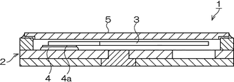
図において、圧電デバイス1は、セラミック製の浅い箱状のパッケージ2内に電極部4を形成し、この電極部4に導電性接着剤4aを用いて、圧電振動片3を固定している。このパッケージ2は、ガラス製の透明な蓋体5により気密に封止されている。
そして、蓋体5の封止後に外部からレーザ光を蓋体5を介してパッケージ2内に照射し、圧電振動片3に形成されている電極の一部を蒸散させることにより、周波数調整することができるようになっている。
In the figure, the
After the lid 5 is sealed, the frequency is adjusted by irradiating the package 2 with laser light from the outside through the lid 5 and evaporating a part of the electrodes formed on the piezoelectric vibrating
ところが、このような構造の圧電デバイス1においては、蓋体5がガラスで形成されており、この比較的脆い材質の蓋体5が外部に大きく露出する状態である。このため、ガラス製の蓋体5に何かが衝突するなどした場合には、蓋体5に割れや欠けが生じて、封止状態に影響し、振動性能を損なう場合がある。
However, in the
このような弊害に対しては、例えば、図13に示すような蓋体6を使用することも考えられる(特許文献2参照)。
図13(a)は蓋体6の概略断面図、図13(b)は蓋体6の概略平面図である。
図において、蓋体6は金属などの丈夫な損傷にくい材料により形成されており、窓と成る開口8が形成されている。この開口8には、ガラス7が充填されており、このガラス7を利用して、外部からレーザ光を照射することができるようになっている。これにより、蓋体6を上述したパッケージ2等に接合することで、上述した弊害を防止しようとするものである。
For such a harmful effect, for example, it may be possible to use a
FIG. 13A is a schematic sectional view of the
In the figure, the
このように、蓋体やパッケージの一部を透明にした構造を得るためには、例えば、半導体レーザの発生装置などにおいて、次のような構造が紹介されている(特許文献3参照)。すなわち、レーザーダイオードチップを封止するパッケージをキャップ状の金属により形成し、このキャップ状のパッケージに光透過窓を形成したものである。
この場合、その製造方法は、キャップ状のパッケージに開口を形成し、ガラスタブレットをこの開口に嵌めて、加熱することにより溶融させて接合するというものである。
Thus, in order to obtain a structure in which a part of the lid and the package is made transparent, for example, the following structure is introduced in a semiconductor laser generator (see Patent Document 3). That is, a package for sealing a laser diode chip is formed of a cap-shaped metal, and a light transmission window is formed on the cap-shaped package.
In this case, the manufacturing method is such that an opening is formed in a cap-shaped package, a glass tablet is fitted into the opening, and is melted and joined by heating.
ところが、このような手法によると、製造工程でガラスタブレットをはめ込める開口の孔径には限度があり、0.5mmよりも小さくすることは困難で、圧電デバイスについて大幅に小型化を進める上では、使用できない手法である。また、小径にされた開口に、ガラスタブレットを位置決めしてはめ込むことも困難であり、さらに、ガラスタブレットを溶融した後で硬化した表面を研磨することも、小さすぎて難しい。 However, according to such a technique, there is a limit to the hole diameter of the opening in which the glass tablet can be fitted in the manufacturing process, and it is difficult to make it smaller than 0.5 mm, and in order to greatly reduce the size of the piezoelectric device, This method cannot be used. In addition, it is difficult to position and fit the glass tablet in the small-diameter opening, and it is also difficult to polish the hardened surface after melting the glass tablet.
本発明は、以上の課題を解決するためになされたもので、金属製の丈夫な蓋体に形成される小さな開口に適切にガラスを充填して、加熱用光ビームを透過させることができる構造を実現して、破損しにくい蓋体を複数個同時に形成することができるようにした蓋体および圧電デバイスの製造方法を提供することを目的とする。 The present invention has been made to solve the above-described problems, and is a structure in which a small opening formed in a strong metal lid is appropriately filled with glass so that a heating light beam can be transmitted. It is an object of the present invention to provide a lid body and a method for manufacturing a piezoelectric device that can simultaneously form a plurality of lid bodies that are not easily damaged.
上述の目的は、第1の発明にあっては、少なくとも複数個の蓋体を分離できる大きさの金属基板に、少なくとも前記蓋体の数に対応した数の貫通孔を形成する工程と、前記金属基板に対応して、これとほぼ同じ大きさの1枚のガラス板を前記金属基板に重ねて配置する工程と、前記ガラス板を溶融することにより、前記各貫通孔内に溶融したガラス材料を充填する工程と、個々の前記蓋体の大きさとなるように前記金属基板を切断する工程とを含んでおり、さらに、前記ガラス板を前記金属基板に重ねて配置する工程において、使用されるガラス板が、溶融ガラスの充填に必要とされる厚みよりも厚い板厚のガラス板が使用され、前記貫通孔に前記溶融したガラス材料を充填する工程の後で、前記ガラス板の表面を鏡面研磨して、厚みを薄くし、続いて、前記金属基板の前記貫通孔の周縁部と、該金属基板の下面全体を覆う大きさで、耐蝕膜を形成し、該耐蝕膜から露出したガラス材料をウエットエッチングにより除去することにより、前記貫通孔の周囲に露出するガラスにフランジ部を形成する蓋体の製造方法により、達成される。
第1の発明の構成によれば、少なくとも複数の蓋体を分離できる金属基板を加工するので、複数枚もしくは多数枚の蓋体を一度に加工することができ、加工効率に優れている。しかも貫通孔に充填する光透過物としてのガラスは、大きなガラス板を前記金属基板に重ねた状態で溶融させることにより、充填するので、従来のように個々の開口にガラスタブレットを位置決めして、嵌め込む必要がなく、蓋体の小型化が進み、前記貫通孔が極めて小さな貫通孔でなる開口とされても、ガラス材料を困難なく充填することができる。このようにして形成される蓋体は金属製であり、ガラスよりも構造的に強い材料で形成されているので、外部から何かが衝突した場合に、容易に損傷することがなく、封止性能を損なうことが有効に防止される。また蓋体には、貫通孔にガラス材料を充填した調整用窓部が形成されるので、この窓部を透過させて加熱用光ビームを照射することができる。
しかも、使用されるガラス板が、溶融ガラスの充填に必要とされる厚みよりも厚い板厚のガラス板が使用され、前記貫通孔に前記溶融したガラス材料を充填する工程の後で、前記ガラス板の表面を鏡面研磨して、厚みを薄くしている。このため、貫通孔へ重点されるガラスの充填量を確実に得ることができる。また、金属基板の前記貫通孔の周縁部と、該金属基板の下面全体を覆う大きさで、耐蝕膜を形成し、該耐蝕膜から露出したガラス材料をウエットエッチングにより除去することにより、前記貫通孔の周囲に露出するガラスにフランジ部を形成するようにしている。このため、ガラスを蓋体に固定するうえでアンカー効果を高めて確実な固定をすることができる。
かくして、金属製の丈夫な蓋体に形成される小さな開口に適切にガラスを充填して、加熱用光ビームを透過させることができる構造を実現して、破損しにくい蓋体を複数個同時に形成することができるようにした蓋体の製造方法を提供することができる。
According to the first aspect of the present invention, in the first invention, a step of forming at least a number of through holes corresponding to the number of lids on a metal substrate having a size capable of separating at least a plurality of lids, Corresponding to the metal substrate, a step of arranging a glass plate of approximately the same size as this on the metal substrate, and a glass material melted in each through hole by melting the glass plate And a step of cutting the metal substrate so as to be the size of each of the lid bodies, and further used in a step of placing the glass plate on the metal substrate. A glass plate having a thickness greater than that required for filling the molten glass is used, and the surface of the glass plate is mirror-finished after the step of filling the molten glass material into the through-holes. Polish and thin Subsequently, a corrosion-resistant film is formed in a size that covers the peripheral portion of the through hole of the metal substrate and the entire lower surface of the metal substrate, and the glass material exposed from the corrosion-resistant film is removed by wet etching. This is achieved by a method for manufacturing a lid body in which a flange portion is formed on the glass exposed around the through hole .
According to the configuration of the first invention, since the metal substrate capable of separating at least a plurality of lids is processed, a plurality or a large number of lids can be processed at a time, and the processing efficiency is excellent. In addition, the glass as a light transmitting material to be filled in the through hole is filled by melting a large glass plate overlaid on the metal substrate, so that the glass tablet is positioned at each opening as in the past, There is no need to fit, and even if the lid is downsized and the through hole is an opening made of a very small through hole, the glass material can be filled without difficulty. The lid formed in this way is made of metal and made of a material that is structurally stronger than glass, so if something collides from the outside, it will not be easily damaged and sealed Impairing performance is effectively prevented. Moreover, since the adjustment window part which filled the glass material in the through-hole is formed in the cover body, the light beam for a heating can be irradiated through this window part.
In addition, a glass plate having a thickness greater than that required for filling the molten glass is used, and after the step of filling the through glass with the molten glass material, the glass is used. The surface of the plate is mirror-polished to reduce the thickness. For this reason, it is possible to reliably obtain the glass filling amount focused on the through hole. In addition, a corrosion-resistant film is formed in a size that covers the peripheral portion of the through-hole of the metal substrate and the entire lower surface of the metal substrate, and the glass material exposed from the corrosion-resistant film is removed by wet etching, thereby allowing the penetration. A flange portion is formed on the glass exposed around the hole. For this reason, when fixing glass to a cover body, an anchor effect can be improved and it can fix reliably.
In this way, a small opening formed in a strong metal lid is properly filled with glass to realize a structure that can transmit the heating light beam, and a plurality of lids that are not easily damaged are formed simultaneously. It is possible to provide a method of manufacturing a lid that can be used.
また、上記目的は、第2の発明にあっては、パッケージ内に圧電振動片を収容し、蓋体により気密に封止した圧電デバイスの製造方法であって、前記パッケージと、前記圧電振動片と、前記蓋体とを別々に形成するための個別の形成工程と、前記パッケージを構成する絶縁性基体に対して、前記圧電振動片を接合する工程と、前記パッケージを前記蓋体により気密に封止する蓋封止工程と、前記パッケージの外部から前記圧電振動片に形成されている金属膜に加熱用光ビームを照射する周波数調整工程とを備えており、前記蓋体の形成工程においては、少なくとも複数個の蓋体を分離できる大きさであって、前記パッケージと熱膨張係数が実用上同じ金属材料でなる金属基板に、前記蓋体の数に対応した数の貫通孔を形成する工程と、前記金属基板に対応して、これとほぼ同じ大きさの1枚のガラス板を前記金属基板に重ねて配置する工程と、前記ガラス板を溶融することにより、前記各貫通孔内に溶融したガラス材料を充填する工程と、個々の前記蓋体の大きさとなるように前記金属基板を切断する工程とを含んでおり、さらに、前記ガラス板を前記金属基板に重ねて配置する工程において、使用されるガラス板が、溶融ガラスの充填に必要とされる厚みよりも厚い板厚のガラス板が使用され、前記貫通孔に前記溶融したガラス材料を充填する工程の後で、前記ガラス板の表面を鏡面研磨して、厚みを薄くし、続いて、前記金属基板の前記貫通孔の周縁部と、該金属基板の下面全体を覆う大きさで、耐蝕膜を形成し、該耐蝕膜から露出したガラス材料をウエットエッチングにより除去することにより、前記貫通孔の周囲に露出するガラスにフランジ部を形成するとともに、かつ前記周波数調整工程においては、前記蓋体の開口に充填した前記ガラス材料を介して、前記パッケージ内の前記圧電振動片の前記金属膜に対して、前記パッケージの外部から加熱用光ビームを照射し、前記金属膜の一部を蒸散させることにより、周波数調整する、圧電デバイスの製造方法により、達成される。 According to a second aspect of the present invention, there is provided a method of manufacturing a piezoelectric device in which a piezoelectric vibrating piece is accommodated in a package and hermetically sealed by a lid, the package and the piezoelectric vibrating piece And an individual forming step for separately forming the lid, a step of bonding the piezoelectric vibrating piece to the insulating base constituting the package, and the package being hermetically sealed by the lid A lid sealing step for sealing, and a frequency adjusting step for irradiating a heating light beam to the metal film formed on the piezoelectric vibrating piece from the outside of the package. In the lid forming step, Forming a number of through-holes corresponding to the number of the lids on a metal substrate that is of a size that allows separation of at least a plurality of lids and has a thermal expansion coefficient that is practically the same as that of the package. And the gold In response to the substrate, this and the step of substantially place the same size one glass plate of the overlapping on the metal substrate by melting the glass plate, the molten glass material in said respective through holes Glass used in the step of filling and the step of cutting the metal substrate so as to be the size of each of the lids, and further placing the glass plate on the metal substrate. A glass plate having a thickness greater than that required for filling the molten glass is used, and after the step of filling the molten glass material into the through hole, the surface of the glass plate is mirror-polished. Then, reducing the thickness, and subsequently forming a corrosion-resistant film with a size covering the peripheral edge of the through hole of the metal substrate and the entire lower surface of the metal substrate, and exposing the glass material exposed from the corrosion-resistant film. By wet etching By removed by, to form a flange portion on the glass that is exposed around the through hole, and in said frequency adjustment step, through the glass material filled into the opening of the lid, the said package This is achieved by a piezoelectric device manufacturing method in which the frequency is adjusted by irradiating the metal film of the piezoelectric vibrating piece with a heating light beam from the outside of the package and evaporating a part of the metal film. .
第2の発明の構成によれば、蓋体の形成工程において、金属製の蓋体に周波数調整に用いる開口を設けているので、極めて薄い蓋体でも外部からの衝撃に強く、かつガラスを充填した開口を設けておくことができる。このため、蓋封止後の周波数調整工程では、外部からの加熱用光ビームを光を透過するガラスを介して、パッケージ内の圧電振動片の金属膜に照射することができる。このようにして、蓋封止後に周波数調整されて、精密な周波数合わせを行った圧電デバイスは、蓋体がガラスではないので外部からの衝撃に強く、容易に破損されることがない。
この場合、その蓋体の形成工程では、少なくとも複数の蓋体を分離できる金属基板を加工するので、複数枚もしくは多数枚の蓋体を一度に加工することができ、加工効率に優れている。しかも貫通孔に充填する光透過物としてのガラスは、大きなガラス板を前記金属基板に重ねた状態で溶融させることにより、充填するので、従来のように個々の開口にガラスタブレットを位置決めして、嵌め込む必要がなく、蓋体の小型化が進み、前記貫通孔が極めて小さな貫通孔でなる開口とされても、ガラス材料を困難なく充填することができる。
しかも、使用されるガラス板が、溶融ガラスの充填に必要とされる厚みよりも厚い板厚のガラス板が使用され、前記貫通孔に前記溶融したガラス材料を充填する工程の後で、前記ガラス板の表面を鏡面研磨して、厚みを薄くしている。このため、貫通孔へ重点されるガラスの充填量を確実に得ることができる。また、金属基板の前記貫通孔の周縁部と、該金属基板の下面全体を覆う大きさで、耐蝕膜を形成し、該耐蝕膜から露出したガラス材料をウエットエッチングにより除去することにより、前記貫通孔の周囲に露出するガラスにフランジ部を形成するようにしている。このため、ガラスを蓋体に固定する上で、アンカー効果を高めて確実な固定をすることができる。
According to the configuration of the second invention, in the lid forming step, the metal lid is provided with an opening used for frequency adjustment, so even a very thin lid is resistant to external impact and filled with glass. Opening can be provided. For this reason, in the frequency adjustment step after the lid is sealed, the metal film of the piezoelectric vibrating piece in the package can be irradiated with an external heating light beam through the glass that transmits light. Thus, the piezoelectric device that has been frequency-adjusted after lid sealing and has performed precise frequency matching is resistant to external impact because the lid is not made of glass, and is not easily damaged.
In this case, in the lid forming step, a metal substrate capable of separating at least a plurality of lids is processed, so that a plurality or a large number of lids can be processed at a time, and the processing efficiency is excellent. In addition, the glass as a light transmitting material to be filled in the through hole is filled by melting a large glass plate overlaid on the metal substrate, so that the glass tablet is positioned at each opening as in the past, There is no need to fit, and even if the lid is downsized and the through hole is an opening made of a very small through hole, the glass material can be filled without difficulty.
In addition, a glass plate having a thickness greater than that required for filling the molten glass is used, and after the step of filling the through glass with the molten glass material, the glass is used. The surface of the plate is mirror-polished to reduce the thickness. For this reason, it is possible to reliably obtain the glass filling amount focused on the through hole. In addition, a corrosion-resistant film is formed in a size that covers the peripheral portion of the through-hole of the metal substrate and the entire lower surface of the metal substrate, and the glass material exposed from the corrosion-resistant film is removed by wet etching, thereby allowing the penetration. A flange portion is formed on the glass exposed around the hole. For this reason, when fixing glass to a cover body, an anchor effect can be heightened and it can fix reliably.
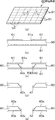
図1及び図2は、本発明の圧電デバイスの実施形態を示しており、図1はその概略平面図、図2は図1のA−A線概略断面図、図3は図1の圧電デバイスのパッケージに収容される圧電振動片の概略斜視図、図4は図3のB−B線切断端面図である。
図において、圧電デバイス30は、圧電振動子を構成した例を示しており、圧電デバイス30は、パッケージ37内に圧電振動片32を収容している。パッケージ37は、例えば、後述するように、絶縁材料として、酸化アルミニウム質のセラミックグリーンシートを成形して形成される複数の基板を積層した後、焼結して形成されている。
1 and 2 show an embodiment of the piezoelectric device of the present invention, FIG. 1 is a schematic plan view thereof, FIG. 2 is a schematic cross-sectional view taken along line AA of FIG. 1, and FIG. 3 is a piezoelectric device of FIG. 4 is a schematic perspective view of a piezoelectric vibrating piece housed in the package, and FIG. 4 is an end view taken along the line BB of FIG.
In the figure, the
すなわち、この実施形態では、パッケージ37は、第1の基板55と第2の基板56とを積層して形成されており図2に示す全長L1が例えば約2.0mmときわめて小さいものである。パッケージ37は、図2に示すように、第2の基板56の内側の材料を除去することで、内部空間Sのスペースを形成している。この内部空間Sが圧電振動片32を収容するための収容空間である。そして、第1の基板55が絶縁性基体に相当し、この第1の基板55に圧電振動片32を接合している。
That is, in this embodiment, the
パッケージ37の内部空間S内の図において左端部付近において、内部空間Sに露出して内側底部を構成する絶縁性基体としての第1の基板55には、例えば、タングステンメタライズ上にニッケルメッキ及び金メッキで形成した電極部31,31が設けられている。
この電極部31,31は、それぞれ図2に示す実装端子48,48と接続されており、外部から印加される駆動電圧を、圧電振動片32に供給するものである。具体的には、この実装端子48,48と電極部31,31は、パッケージ37外部をメタライズにより引き回したり、あるいは第1の基板55および第2の基板56の焼成前にタングステンメタライズ等を利用して形成した導電スルーホール等で接続することで形成できる。
各電極部31,31の上には、導電性接着剤47が塗布されて、圧電振動片32の基部51が接合されている。この導電性接着剤47としては、例えば、合成樹脂などを利用したバインダー成分に、銀粒子などの導電粒子を混入したもので、機械的接合と電気的接続とを同時に行うことができるものである。
For example, nickel plating and gold plating on tungsten metallization are applied to the
The electrode portions 31 and 31 are connected to the mounting
A conductive adhesive 47 is applied on each electrode portion 31, and the
圧電振動片32は、例えば水晶で形成されており、水晶以外にもタンタル酸リチウム,ニオブ酸リチウム等の圧電材料を利用することができる。本実施形態の場合、圧電振動片32は、小型に形成して、必要な性能を得るために、特に図3に詳しく示す形状とされている。
すなわち、圧電振動片32は、パッケージ37側と固定される基部51と、この基部51を基端として、図において斜め右方に向けて、二股に別れて平行に延びる一対の振動腕35,36を備えており、全体が音叉のような形状とされた、所謂、音叉型圧電振動片が利用されている。
The piezoelectric vibrating
That is, the piezoelectric vibrating
ここで、各振動腕35,36の主面には、好ましくは、それぞれ長さ方向に延びる長溝33,34を形成し、この長溝内に励振電極38,39を形成している。この長溝は、それぞれ振動腕35と、振動腕36の主面である表裏面に形成され、図4に示すように、長溝33,34内には励振電極38,39がそれぞれ形成されており、各振動腕の長溝内に形成される励振電極は互いに分離された一対の電極とされている。これにより、励振電極に駆動電圧が印加されることによって、駆動時に、各振動腕の内部の電界効率を高めることができるようになっている。
Here,
また、圧電振動片32の基部51の端部(図1では左端部)の幅方向両端付近には、上述したように、パッケージ37の電極部31,31と接続するための電極部として、引出し電極38a,39aが形成されている。各引出し電極38a,39aは、基部51の外縁を回り込んで、圧電振動片32の基部51の表裏に設けられている。これらの各引出し電極38a,39aは上述した各励振電極と接続されており、例えば、水晶表面に、クロム(Cr)および金(Au)を順次メッキして形成することができる。また、振動腕35,36の少なくとも表面の先端領域には、この電極金属と同じ金属を利用して、電極形成の際に同時に周波数調整用の金属膜53,54が形成されている。
Further, as described above, a lead-out is provided near both ends in the width direction of the end portion (left end portion in FIG. 1) of the
これにより、引出し電極38a,39aから、励振電極38,39に駆動電圧が印加されることにより、各振動腕35,36内で電界が適切に形成され、振動腕35,36の各先端部が互いに接近したり離間したりするように駆動されて、所定の周波数で振動する。
尚、圧電振動片としては、図示のような音叉型の圧電振動片に限らず、圧電材料を矩形にカットしたATカット振動片やコンベックスタイプの振動片等の種々の圧電振動片を使用することができる。
As a result, a drive voltage is applied to the
The piezoelectric vibrating piece is not limited to the tuning-fork type piezoelectric vibrating piece as shown in the figure, and various piezoelectric vibrating pieces such as an AT cut vibrating piece obtained by cutting a piezoelectric material into a rectangular shape or a convex type vibrating piece may be used. Can do.
パッケージ37の開放された上端には、蓋体40が接合されることにより、封止されている。
蓋体40は、その厚みが極めて薄く形成されており、例えば、厚み0.1mm以下とされている。また蓋体40の材料は、ガラス材料よりも割れにくい丈夫な材料で形成されており、後述する金属基板を加工して形成されている。そして、好ましくは、蓋体40を形成するための材料として、パッケージ37の材料と熱膨張係数が近似したものが選択される。このような条件を満たすものとして、例えば、鉄,ニッケル,コバルトの合金であるコバール合金が適している。
A
The
この蓋体40には、図1および図2に示すように、周波数調整用窓部(以下、「窓部」という)41が形成されている。窓部41は、図示されているように蓋体40を表裏に貫通する貫通孔42であり、好ましくは、図示されているように、外側に向かって徐々に縮径するテーパ状とされている。
貫通孔42をこのようなテーパ状とすると、そうでない場合と比べて、後述するガラスと貫通孔42との接合面積が増大し、接合強度を向上させることができる。また開口の形状は円形に限らず、長円形や楕円、多角形などでもよい。とくに、貫通孔42の開口部が小さな曲面の連続となるような形状であると、貫通孔42の内面の面積を増大することができて好ましい。
そして、窓部41の形成される個所は、蓋体40がパッケージ37を封止した状態で、内部に収容されている圧電振動片32の周波数調整用の金属膜と対向する位置に設けられる。この場合、圧電振動片32の振動腕36および/または35の先端領域と対向する個所である。図1に示されているように、好ましくは、貫通孔42は、各振動腕35,36の先端領域の金属膜(後述)が開口内に入る位置に形成され、開口径もこれら金属膜を露出させる大きさとされる。
貫通孔42の内周面は粗面42aとされている。粗面42aは貫通孔42の内周面の表面粗さを意図的に粗くしたものであって、平坦な面よりも摩擦が大きくなるようにしたものである。
As shown in FIGS. 1 and 2, the
When the through
And the part in which the
The inner peripheral surface of the through
そして、このような貫通孔42には、ガラス43が取付けられている。ガラス43は、後述する周波数調整に使用される加熱用光ビームとして、レーザ光や、ハロゲンビームなどの加熱用の光ビームを透過させる性質を備えるものであれば、種々のものが使用できるが、加工の容易さや、コストなどを考慮するとともに、特に蓋体40を構成する材料と、熱膨張係数が近似したものを選択することが好ましい。このような点で、使用されるガラスとしては、硼珪酸ガラスや、コバールガラス等が用いられる。この実施形態では、好ましくは、ガラス43の貫通孔42に挿入される挿入部46の下端には、貫通孔42に挿入されない部分として、貫通孔42の内径よりも大きな外径を有するフランジ部44が設けられている。そして、ガラス43はその外周とフランジ部44の上向き段部44aとで直接蓋体40に直接接合されている。
A
蓋体40が、コバール等の金属材料で形成される場合には、蓋体40はシーム溶接等の手法により、パッケージ37に対して固定される。あるいは、例えば、蓋体40の表面にニッケル及び金メッキを施し、ロウ材37aとして、金スズ合金(Au−Sn)を用いて接合するようにしてもよい。
When the
本実施形態は以上のように構成されており、圧電デバイス30のパッケージ37を封止するための蓋体40は金属というガラスよりも構造的に強い材料で形成されているので、外部から何かが衝突した場合に、容易に損傷することがなく、パッケージ37の封止性能を損なうことが有効に防止される。
また蓋体40には、貫通孔42にガラス43を取付けることにより形成した調整用窓部41を備えているから、この窓部41を透過させてパッケージ内部の圧電振動片32に形成した金属膜53,54に対して、図2に符号LBで示すようにレーザ光やハロゲンビームなどの加熱用光ビームを照射することができる。この場合、蓋体40がその厚みを極めて薄くするように形成されていて、貫通孔42の内側に段部を設けることができない場合であっても、貫通孔42とガラス43との接触面が粗面42aとされているので、この粗面を利用して、ガラス43を直接その摩擦力で保持し、そのアンカー効果を効果的に高めて保持することができる。
This embodiment is configured as described above, and the
Further, since the
かくして、パッケージ37を封止するための丈夫な材料で形成したきわめて厚みの薄い蓋体40で封止したパッケージ37を備える圧電デバイス30であって、蓋体40の外部からパッケージ37内にレーザ光LBなどを透過させて、質量削減方式による周波数調整をすることができる構造を実現することができる。
さらに、図2で説明したように、好ましくは、ガラス43がフランジ部44を備えている。
このため、上述の作用効果に加えて、ガラス43は、貫通孔42に挿入される挿入部46の外周とフランジ部44の貫通孔42周縁部への当接面である上向き段部44aの箇所で、蓋体40に対して接合されるので、接合面積が増大することで、より確実で接合強度の高い固定構造とすることができる。
しかもフランジ部44はガラス43の下部に設けられているので、蓋体40の内側におさまり、圧電デバイス30の外形を拡大させることがないので、表面実装される圧電デバイス30の高さ方向の大きさをコンパクトに納めることができる。
Thus, in the
Further, as described with reference to FIG. 2, the
For this reason, in addition to the above-described effects, the
Moreover, since the
図5は上述の第1の実施形態の圧電デバイスの変形例を示す概略断面図である。
図5の圧電デバイス30−1は、ガラス43の形状を除き、第1の実施形態の圧電デバイス30と同じ構造であるから、共通する構成には同一の符号を付して重複する説明は省略し、以下、相違点を中心に説明する。
この圧電デバイス30−1においては、蓋体40の貫通孔42に取付けられるガラス43の上端にフランジ部44−1が形成され、このフランジ部44−1は、蓋体40の外部に突出している。また、貫通孔42は、蓋体40の外方に徐々に拡径するテーパ状に形成されている。したがって、この外方への突出分だけ圧電デバイス30−1の高さ方向の寸法を拡大させることとなるが、その分パッケージ37の内部空間Sは大きくなり、圧電振動片32の振動腕35の先端部が上方に振れた際に、フランジ部と当接する事態を有効に避けることができる。それ以外の作用効果は、第1の実施形態の圧電デバイス30と同じである。
FIG. 5 is a schematic sectional view showing a modification of the piezoelectric device of the first embodiment.
Since the piezoelectric device 30-1 in FIG. 5 has the same structure as the
In the piezoelectric device 30-1, a flange portion 44-1 is formed at the upper end of the
(圧電デバイスの製造方法)
次に、圧電デバイス30(30−1)の製造方法の実施形態を図6のフローチャートを参照しながら説明する。
先ず、図1ないし図6で説明した圧電振動片32と蓋体40、パッケージ37は、それぞれ別々に形成しておく。
(圧電振動片の形成工程)
圧電振動片32については、例えば、水晶ウエハをエッチングして、既に説明した形状を形成するとともに、必要な励振電極を形成する(ST11)ことで、従来と同様に製造することができるので、詳しい説明は省略する。電極形成後に、駆動電圧を印加して周波数を粗調整する(ST12)。
(パッケージの形成工程)
図1および図2で説明したパッケージ37は、例えば、所定の溶液中にセラミックパウダを分散させ、バインダを添加して生成される混練物をシート状の長いテープ形状に成形し、これを所定の長さにカットして得た、所謂グリーンシートを用意する。
グリーンシートは、上述した第1の基板55と、第2の基板56とを形成するために共通して使用することができる。
(Piezoelectric device manufacturing method)
Next, an embodiment of a method for manufacturing the piezoelectric device 30 (30-1) will be described with reference to the flowchart of FIG.
First, the piezoelectric vibrating
(Piezoelectric vibrating piece forming process)
The piezoelectric vibrating
(Package formation process)
The
The green sheet can be commonly used for forming the
これら第1の基板55と、第2の基板56は、上述した各構造に適合するように成形され、各電極部や導電パターンを形成する。すなわち、第1の基板55となるグリーンシートには、裏側に実装端子48,48に対応して、導電ペースト、例えばタングステンメタライズを塗布する。表側には電極部31,31に対応して、タングステンメタライズを塗布する。さらに必要に応じてスルーホールを穿設し、導電ペーストを塗布することで、導電スルーホールを形成する。第2の基板56となるグリーンシートは、内部空間Sに対応するように、材料を除去する。
成形後に第1および第2の基板を積層し、焼成後、タングステンメタライズ上に、ニッケルおよび金メッキを施す。なお、蓋体側に封止材を設けない場合には、パッケージ37の上端に、封止材として、例えば、金スズ合金(Au−Sn)37aを設けておく。あるいは、蓋体40をシームリングで封止する場合には、シームリング37aを設けておくことになる。
The
After the molding, the first and second substrates are laminated, and after firing, nickel and gold are plated on the tungsten metallization. In the case where the sealing material is not provided on the lid side, for example, a gold tin alloy (Au—Sn) 37 a is provided on the upper end of the
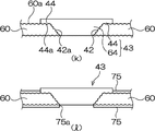
(蓋体の形成工程)
蓋体40をコバールの板材を用いて形成する場合について説明する。
図7(a)に示すように、コバール製の金属基板を用意する。この金属基板60は、点線で示す縦横の複数の切断線で、後述するように切断されることで、切り離されるB1の部分が、上述した個々の蓋体40と対応する大きさであり、複数もしくは多数個取りの金属基板である。この金属基板60は、製品の高さ方向の大きさを抑制しつつ必要な強度を得るために、その板厚が、例えば、0.08ないし0.1mm程度とすることが好ましい。
(Cover forming process)
A case where the
As shown in FIG. 7A, a Kovar metal substrate is prepared. The
以下の工程では、理解の便宜のため、図7(a)のC−C線切断端面図の箇所だけを拡大して図示することにより説明するが、これらの構成は、金属基板60の全体において、同時に進行し、金属基板60に含まれる全てのB1に関して処理が同時に行われるものである。
図7(b)に示すように、金属基板60の表面および裏面にフォトレジスト61を塗布する。この場合、いずれかの面(図示では表面)に、開口部61aを形成したパターンとする(ST21)。
次に、コバールをエッチングできるエッチング液に浸漬し、開口部61aが形成された側に相当する片面から、ウエットエッチングする(ST22)。エッチング液としては、例えば、鉄合金やニッケル合金のエッチング液が使用でき、塩化第二鉄溶液等を使用することができる。あるいは、この場合、片面からプラズマイオンエッチングなどによるドライエッチングを行ってもよい。
これにより、図7(c)に示すように、厚み方向のエッチングとともに、開口部61aの周縁部に沿ってサイドエッチングが進行するので、深さ方向に沿って徐々に縮径するテーパ状の貫通孔42が形成される。これと同時に、貫通孔42の内面は粗面42aとなって貫通孔42が穿設される。
In the following steps, for convenience of understanding, description will be made by enlarging and illustrating only the portion of the end view taken along the line CC in FIG. 7A. The processes proceed simultaneously, and all the B1 included in the
As shown in FIG. 7B, a
Next, the Kovar is immersed in an etching solution that can be etched, and wet etching is performed from one side corresponding to the side where the
As a result, as shown in FIG. 7C, since the side etching proceeds along the peripheral edge of the
次いで、図7(d)に示すように、レジストを剥離したら(ST23)、図7(e)に示すように、上述したエッチング液にふたたび浸漬し、貫通孔42を形成した金属基板60の露出面全体をエッチング(ST24)する。このエッチングの目的は、金属基板60の露出表面全体の粗面化であるから、貫通孔42の穿設の際のエッチング時間よりも短い時間でよい。
これにより、金属基板60の表裏面が粗面60aとされる。
Next, as shown in FIG. 7D, after the resist is peeled off (ST23), as shown in FIG. 7E, the
Thereby, the front and back surfaces of the
続いて、図8(f)に示すように、金属基板60の上にガラス板62を載せる(ST25)。ここで、ガラス板62は、図7(a)で示した金属基板60とほぼ同じ大きさのものが使用される。以下の工程では、このガラス板62を加熱溶融して、各貫通孔42に同時に溶融ガラスを充填することがねらいであるから、ガラス板62の大きさは、この目的に必要な大きさである。そして、金属基板60とガラス板62の外形寸法を一致させると、作業が容易となる。このガラス板62は、特に蓋体40を構成する材料と、熱膨張係数が近似したものを選択することが好ましく、このような点で、使用されるガラスとしては、硼珪酸ガラスや、コバールガラス等が適している。
ここで、ガラス板62の厚み寸法t1は、比較的厚いものが使用されており、後述するように、貫通孔42に溶融ガラスとして充填するための材料の必要量を確実にするとともに、後述する研磨工程の研磨しろを得るようにしている。このような点から、厚みt1は、蓋体40となる金属基板60の厚みとの関係で、0.1ないし0.2mm程度が好ましい。
Subsequently, as shown in FIG. 8F, a
Here, the thickness t1 of the
次に、図8(f)の状態のものを、適切な加熱手段、例えば、高周波・電気炉などの加熱炉内に収容し、加熱する(ST26)。この加熱は還元炎によるものは使用できず、加熱直前に脱ガス工程を行い、その後、1000ないし1200度(摂氏、以下、温度表記は全て「摂氏」)で、所定時間加熱し、図8(g)に示すように、溶融することで、溶融されたガラス材料がガラス充填部64として、貫通孔42内に充填される。
この状態では、図示のように、ガラス充填部64の下端部65が貫通孔42から露出する場合がある。
Next, the thing of the state of FIG.8 (f) is accommodated in suitable heating means, for example, heating furnaces, such as a high frequency and electric furnace, and is heated (ST26). This heating cannot be performed using a reducing flame, and a degassing step is performed immediately before the heating. Thereafter, heating is performed at 1000 to 1200 degrees (Celsius, hereinafter, all temperature notations are “Celsius”) for a predetermined time, and FIG. As shown in g), the molten glass material is filled into the through
In this state, the
そこで、図8(h)に示すように、溶融ガラスの硬化後において、上記露出した下端65と、図8(g)で示されているガラス板の表面部63の部分を研磨する(ST27)。この研磨工程により、ガラス板62は表面および裏面が鏡面研磨される。
かくして、貫通孔62に充填されたガラス板62は、貫通孔62の内面が粗面62aとされているので、アンカー効果により強固に接合している。しかも、貫通孔42は、テーパ状であり、孔の長さ方向に関して孔径が変わらない孔の場合と比べると、接合面積が増大されていることから、この点においてもガラス板62と貫通孔42との接合強度は高くなっている。
Therefore, as shown in FIG. 8 (h), after the molten glass is hardened, the exposed
Thus, the
次いで、図8(i)に示すように、金属基板60の貫通孔42の周縁部と、図において、下面全体を覆う大きさで、耐蝕膜70を形成する(ST28)。ウエットエッチングによる場合は、耐蝕膜として、例えば、有機レジストを用いることができる。そして、この耐蝕膜70から露出したガラスをウエットエッチングにより除去する(ST29)。
あるいは、このエッチングはドライエッチングによりするようにしてもよい。この場合、金属基板60の貫通孔42の周縁部に耐蝕膜を形成する(図示せず)。この耐蝕膜は、例えば、下地層をクロム(Cr)とし、その上に金(Au)をスパッタリングにより成膜することにより形成することができる。その後、図の上方より片面のドライエッチングで、金属基板60の片面を覆うガラス材料を除去する。このドライエッチングは、例えば、ワークを気密のチャンバー内に収容して、真空排気し、CF4等を充填ガスとして、プラズマ放電によりイオンエッチングすることにより、耐蝕膜から露出したガラス板62を除去することができる。
Next, as shown in FIG. 8 (i), a corrosion-
Alternatively, this etching may be performed by dry etching. In this case, a corrosion resistant film is formed on the periphery of the through
これにより、図8(j)に示すように、貫通孔42への挿入部46とフランジ部44を備えた図2で説明したガラス43が形成され、このフランジ部44は、金属基板60の表面の粗面60aと接合し、そのアンカー効果が高められて、この点においても、強い接合強度が実現される。
次いで、図9(k)に示すように、耐蝕膜を除去し(ST30)、図9(l)に示すように、金属基板60の表面および裏面に、電解メッキによりニッケルで覆う(ST31)。最後に、図7(a)で説明した縦横の点線に沿って、金属基板60を切断することによりそのB1を単位とする蓋体40が完成する。
As a result, as shown in FIG. 8 (j), the
Next, as shown in FIG. 9 (k), the corrosion resistant film is removed (ST30), and as shown in FIG. 9 (l), the front and back surfaces of the
(圧電振動片の接合工程)
次に、圧電振動片32をパッケージ37の電極部31の上に接合する(ST41)。すなわち、図1および図2で説明したように、パッケージ37の電極部31上に導電性接着剤47を塗布して、その上に圧電振動片32の基部51の引き出し電極38a,39aの個所を載置し、導電性接着剤47,47を硬化させることにより、電極部31と圧電振動片32とが電気的、機械的に接合される。このようにして、圧電振動片32は絶縁性基体である第1の基板55に対して、片持ち式に接合される。
(Piezoelectric vibrating piece joining process)
Next, the piezoelectric vibrating
さらに、パッケージ37と蓋体40とを真空雰囲気中で、接合することで蓋封止を行う(ST42)。
図10は電極ローラなどの治具Jを蓋体40に接触させて抑え、シームリング37aをジュール熱で溶融硬化させて、シーム溶接により蓋封止を行う様子を示している。
続いて、図2で説明したように、蓋体40の外部からレーザ光LBなどをガラス43を透過させて、圧電振動片32の図3で説明した金属膜53および/または54に照射し、その一部を蒸散させて、質量削減方式により周波数調整を行う(ST43)。ここで、貫通孔42が、図1に示すように、両振動腕35,36の金属膜を露出させるものであると、各振動腕の金属膜について、その一部を蒸散させることができ、両振動腕35,36についての屈曲バランスまでも調整できて好ましい。
その後必要な検査を経て(ST44)、圧電デバイス30が完成する。
Further, the lid is sealed by bonding the
FIG. 10 shows a state in which a jig J such as an electrode roller is held in contact with the
Subsequently, as described in FIG. 2, the laser beam LB or the like is transmitted from the outside of the
Thereafter, a necessary inspection is performed (ST44), and the
このように、この実施形態に係る圧電デバイスの製造方法では、蓋体40の形成工程において、金属製の蓋体40に周波数調整に用いる開口を設けているので、極めて薄い蓋体40でも外部からの衝撃に強く、かつガラス43を充填した開口を設けておくことができる。このため、蓋封止後の周波数調整工程では、外部からの加熱用光ビームLBを光を透過するガラスを介して、パッケージ37内の圧電振動片32の金属膜に照射することができる。このようにして、蓋封止後に周波数調整されて、精密な周波数合わせを行った圧電デバイス30は、蓋体40がガラスではないので外部からの衝撃に強く、容易に破損されることがない。
この場合、その蓋体40の形成工程では、少なくとも複数の蓋体を分離できる金属基板60を加工するので、複数枚もしくは多数枚の蓋体を一度に加工することができ、加工効率に優れている。しかも貫通孔42に充填するガラス43は、大きなガラス板62を前記金属基板60に重ねた状態で溶融させることにより、充填するので、従来のように個々の開口にガラスタブレットを位置決めして、嵌め込む必要がなく、蓋体の小型化が進み、前記貫通孔が極めて小さな貫通孔でなる開口とされても、ガラス材料を困難なく充填することができる。
As described above, in the piezoelectric device manufacturing method according to this embodiment, since the opening used for frequency adjustment is provided in the
In this case, since the
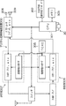
図11は、本発明の上述した実施形態に係る圧電デバイスを利用した電子機器の一例としてのデジタル式携帯電話装置の概略構成を示す図である。
図において、送信者の音声を受信するマイクロフォン308及び受信内容を音声出力とするためのスピーカ309を備えており、さらに、送受信信号の変調及び復調部に接続された制御部としての集積回路等でなるCPU(Central Processing Unit)301を備えている。
CPU301は、送受信信号の変調及び復調の他に画像表示部としてのLCDや情報入力のための操作キー等でなる情報の入出力部302や、RAM,ROM等でなる情報記憶手段(メモリ)303の制御を行うようになっている。このため、CPU301には、圧電デバイス30等の本発明の実施形態や変形例の圧電デバイスが取り付けられて、その出力周波数をCPU301に内蔵された所定の分周回路(図示せず)等により、制御内容に適合したクロック信号として利用するようにされている。このCPU301に取付けられる圧電デバイスは、圧電振動子でも圧電発振器でもよい。
FIG. 11 is a diagram showing a schematic configuration of a digital mobile phone device as an example of an electronic apparatus using the piezoelectric device according to the above-described embodiment of the present invention.
In the figure, a
In addition to modulation and demodulation of transmission / reception signals, the
CPU301は、さらに、温度補償水晶発振器(TCXO)305と接続され、温度補償水晶発振器305は、送信部307と受信部306に接続されている。これにより、CPU301からの基本クロックが、環境温度が変化した場合に変動しても、温度補償水晶発振器305により修正されて、送信部307及び受信部306に与えられるようになっている。
The
このように、制御部を備えたデジタル式携帯電話装置300のような電子機器に、上述した実施形態に係る圧電デバイス30を利用することができる。この場合、外部から衝撃を受けても、蓋体が損傷を受けることがないので、製品の信頼性が向上する。
As described above, the
本発明は上述の実施形態に限定されない。各実施形態の各構成はこれらを適宜組み合わせたり、省略し、図示しない他の構成と組み合わせることができる。
また、この発明は、パッケージや箱状の蓋体に被われるようにして、内部に圧電振動片を収容するものであれば、圧電振動子、圧電発振器等の名称にかかわらず、全ての圧電デバイスに適用することができる。
The present invention is not limited to the above-described embodiment. Each configuration of each embodiment can be appropriately combined or omitted, and can be combined with other configurations not shown.
In addition, the present invention is applicable to all piezoelectric devices regardless of the names of piezoelectric vibrators, piezoelectric oscillators, etc., as long as they are covered with a package or a box-shaped lid and accommodate a piezoelectric vibrating piece inside. Can be applied to.
30,30−1・・・圧電デバイス、32・・・圧電振動片、35,36・・・振動腕、31・・・電極部、40・・・蓋体、41・・・調整用窓部、43・・・ガラス、47・・・導電性接着剤、55・・・第1の基板(絶縁性基体)、56・・・第2の基板。 30, 30-1 ... Piezoelectric device, 32 ... Piezoelectric vibrating piece, 35, 36 ... Vibrating arm, 31 ... Electrode, 40 ... Lid, 41 ... Adjustment window , 43... Glass, 47... Conductive adhesive, 55... First substrate (insulating base), 56.
Claims (2)
前記金属基板に対応して、これとほぼ同じ大きさの1枚のガラス板を前記金属基板に重ねて配置する工程と、
前記ガラス板を溶融することにより、前記各貫通孔内に溶融したガラス材料を充填する工程と、
個々の前記蓋体の大きさとなるように前記金属基板を切断する工程と
を含んでおり、
さらに、前記ガラス板を前記金属基板に重ねて配置する工程において、使用されるガラス板が、溶融ガラスの充填に必要とされる厚みよりも厚い板厚のガラス板が使用され、
前記貫通孔に前記溶融したガラス材料を充填する工程の後で、前記ガラス板の表面を鏡面研磨して、厚みを薄くし、
続いて、前記金属基板の前記貫通孔の周縁部と、該金属基板の下面全体を覆う大きさで、耐蝕膜を形成し、該耐蝕膜から露出したガラス材料をウエットエッチングにより除去することにより、前記貫通孔の周囲に露出するガラスにフランジ部を形成する
ことを特徴とする、蓋体の製造方法。 Forming at least a number of through holes corresponding to the number of lids on a metal substrate having a size capable of separating at least a plurality of lids;
Corresponding to the metal substrate, a step of placing a single glass plate of approximately the same size on the metal substrate,
Filling the melted glass material into each through hole by melting the glass plate;
Cutting the metal substrate so as to be the size of each individual lid, and
Further, in the step of placing the glass plate on the metal substrate, a glass plate having a thickness greater than the thickness required for filling the molten glass is used,
After the step of filling the through hole with the molten glass material, the surface of the glass plate is mirror-polished to reduce the thickness,
Subsequently, by forming a corrosion-resistant film in a size that covers the peripheral portion of the through hole of the metal substrate and the entire lower surface of the metal substrate, and removing the glass material exposed from the corrosion-resistant film by wet etching, A flange part is formed in the glass exposed around the through hole. A method for manufacturing a lid.
前記パッケージと、前記圧電振動片と、前記蓋体とを別々に形成するための個別の形成工程と、
前記パッケージを構成する絶縁性基体に対して、前記圧電振動片を接合する工程と、
前記パッケージを前記蓋体により気密に封止する蓋封止工程と、
前記パッケージの外部から前記圧電振動片に形成されている金属膜に加熱用光ビームを照射する周波数調整工程と
を備えており、
前記蓋体の形成工程においては、
少なくとも複数個の蓋体を分離できる大きさであって、前記パッケージと熱膨張係数が実用上同じ金属材料でなる金属基板に、少なくとも前記蓋体の数に対応した数の貫通孔を形成する工程と、
前記金属基板に対応して、これとほぼ同じ大きさの1枚のガラス板を前記金属基板に重ねて配置する工程と、
前記ガラス板を溶融することにより、前記各貫通孔内に溶融したガラス材料を充填する工程と、
個々の前記蓋体の大きさとなるように前記金属基板を切断する工程と
を含んでおり、
さらに、前記ガラス板を前記金属基板に重ねて配置する工程において、使用されるガラス板が、溶融ガラスの充填に必要とされる厚みよりも厚い板厚のガラス板が使用され、
前記貫通孔に前記溶融したガラス材料を充填する工程の後で、前記ガラス板の表面を鏡面研磨して、厚みを薄くし、
続いて、前記金属基板の前記貫通孔の周縁部と、該金属基板の下面全体を覆う大きさで、耐蝕膜を形成し、該耐蝕膜から露出したガラス材料をウエットエッチングにより除去することにより、前記貫通孔の周囲に露出するガラスにフランジ部を形成するとともに、
かつ前記周波数調整工程においては、前記蓋体の前記開口に充填した前記ガラス材料を介して、前記パッケージ内の前記圧電振動片の前記金属膜に対して、前記パッケージの外部から加熱用光ビームを照射し、前記金属膜の一部を蒸散させることにより、周波数調整することを特徴とする、圧電デバイスの製造方法。 A method for manufacturing a piezoelectric device in which a piezoelectric vibrating piece is accommodated in a package and hermetically sealed by a lid,
An individual forming step for separately forming the package, the piezoelectric vibrating piece, and the lid;
Bonding the piezoelectric vibrating piece to an insulating substrate constituting the package;
A lid sealing step for hermetically sealing the package with the lid;
And a frequency adjusting step of irradiating a heating light beam to a metal film formed on the piezoelectric vibrating piece from the outside of the package,
In the step of forming the lid,
Forming at least a number of through-holes corresponding to the number of the lids on a metal substrate made of a metal material practically the same in size as the package and having a thermal expansion coefficient that is practically the same as that of the package. When,
Corresponding to the metal substrate, a step of placing a single glass plate of approximately the same size on the metal substrate,
Filling the melted glass material into each through hole by melting the glass plate;
Cutting the metal substrate so as to be the size of each individual lid, and
Further, in the step of placing the glass plate on the metal substrate, a glass plate having a thickness greater than the thickness required for filling the molten glass is used,
After the step of filling the through hole with the molten glass material, the surface of the glass plate is mirror-polished to reduce the thickness,
Subsequently, by forming a corrosion-resistant film in a size that covers the peripheral portion of the through hole of the metal substrate and the entire lower surface of the metal substrate, and removing the glass material exposed from the corrosion-resistant film by wet etching, While forming a flange portion in the glass exposed around the through hole,
In the frequency adjusting step, a heating light beam is applied from the outside of the package to the metal film of the piezoelectric vibrating piece in the package via the glass material filled in the opening of the lid. A method for manufacturing a piezoelectric device, wherein the frequency is adjusted by irradiating and evaporating a part of the metal film.
Priority Applications (1)
| Application Number | Priority Date | Filing Date | Title |
|---|---|---|---|
| JP2003388131A JP4292575B2 (en) | 2003-11-18 | 2003-11-18 | Piezoelectric device and method of manufacturing lid |
Applications Claiming Priority (1)
| Application Number | Priority Date | Filing Date | Title |
|---|---|---|---|
| JP2003388131A JP4292575B2 (en) | 2003-11-18 | 2003-11-18 | Piezoelectric device and method of manufacturing lid |
Publications (2)
| Publication Number | Publication Date |
|---|---|
| JP2005151336A JP2005151336A (en) | 2005-06-09 |
| JP4292575B2 true JP4292575B2 (en) | 2009-07-08 |
Family
ID=34695300
Family Applications (1)
| Application Number | Title | Priority Date | Filing Date |
|---|---|---|---|
| JP2003388131A Expired - Fee Related JP4292575B2 (en) | 2003-11-18 | 2003-11-18 | Piezoelectric device and method of manufacturing lid |
Country Status (1)
| Country | Link |
|---|---|
| JP (1) | JP4292575B2 (en) |
Families Citing this family (7)
| Publication number | Priority date | Publication date | Assignee | Title |
|---|---|---|---|---|
| US7579748B2 (en) | 2006-08-18 | 2009-08-25 | Epson Toyocom Corporation | Piezoelectric device and method for manufacturing thereof |
| JP4978220B2 (en) * | 2007-02-05 | 2012-07-18 | セイコーエプソン株式会社 | Piezoelectric vibrator and manufacturing method thereof |
| JP2008193400A (en) * | 2007-02-05 | 2008-08-21 | Epson Toyocom Corp | Piezoelectric vibrator, and manufacturing method thereof |
| JP2008193581A (en) * | 2007-02-07 | 2008-08-21 | Epson Toyocom Corp | Piezoelectric vibrator, and manufacturing method thereof |
| US7859172B2 (en) | 2007-06-19 | 2010-12-28 | Epson Toyocom Corporation | Piezoelectric resonator, manufacturing method thereof and lid for piezoelectric resonator |
| JP2010093544A (en) * | 2008-10-08 | 2010-04-22 | Nippon Dempa Kogyo Co Ltd | Crystal oscillator for surface mounting |
| JP6488572B2 (en) * | 2014-07-02 | 2019-03-27 | セイコーエプソン株式会社 | Gas cell, gas cell sealing method, and gas cell manufacturing method |
-
2003
- 2003-11-18 JP JP2003388131A patent/JP4292575B2/en not_active Expired - Fee Related
Also Published As
| Publication number | Publication date |
|---|---|
| JP2005151336A (en) | 2005-06-09 |
Similar Documents
| Publication | Publication Date | Title |
|---|---|---|
| JP2004208236A (en) | Piezoelectric device, manufacturing method therefor, portable telephone unit utilizing piezoelectric device and electronic equipment utilizing piezoelectric device | |
| JP4292575B2 (en) | Piezoelectric device and method of manufacturing lid | |
| JP5278044B2 (en) | Package member, method for manufacturing the package member, and piezoelectric vibration device using the package member | |
| JP2005278069A (en) | Piezoelectric vibrating piece and piezoelectric device using it | |
| JP4341268B2 (en) | Package for piezoelectric device, piezoelectric device, mobile phone device using piezoelectric device, and electronic equipment using piezoelectric device | |
| JP3761023B2 (en) | Piezoelectric device and manufacturing method thereof | |
| JP2005136705A (en) | Bonding structure and bonding method for piezoelectric vibrator, piezoelectric device and its manufacturing method, and portable telephone set and electronic apparatus using piezoelectric device | |
| JP2005086783A (en) | Surface mounted piezoelectric device and its package, mobile phone utilizing surface mounted piezoelectric device, and electronic apparatus utilizing surface mounted piezoelectric device | |
| JP4692715B2 (en) | Piezoelectric oscillator, electronic device, and method for manufacturing piezoelectric oscillator | |
| JPWO2010097905A1 (en) | Package manufacturing method, piezoelectric vibrator, oscillator, electronic device, and radio timepiece | |
| JP2005175686A (en) | Method of manufacturing piezoelectric device and lid, portable telephone utilizing piezoelectric device and electronic apparatus utilizing piezoelectric device | |
| JP4114149B2 (en) | Piezoelectric device, manufacturing method thereof, mobile phone device using piezoelectric device, and electronic apparatus using piezoelectric device | |
| JP2005109886A (en) | Piezoelectric device, manufacturing method thereof, cellular telephone apparatus using the same, and electronic apparatus using the same | |
| JP2003069368A (en) | Method for joining piezoelectric device and piezoelectric vibration chip, mobile phone employing the piezoelectric device and electronic device employing the piezoelectric device | |
| JP2004201211A (en) | Joining structure of piezoelectric vibrating piece, piezoelectric device, its manufacturing method, and cellular phone unit and electronic equipment using the device | |
| JP2007235289A (en) | Piezoelectric oscillator | |
| JP3879923B2 (en) | Manufacturing method of lid for electronic parts | |
| JP2004056760A (en) | Piezoelectric device, package for piezoelectric device, manufacture of piezoelectric device, mobile telephone equipment utilizing piezoelectric device and electronic equipment utilizing piezoelectric device | |
| JP2004007198A (en) | Piezoelectric device, package for piezoelectric device, manufacturing method of piezoelectric device, and mobile phone utilizing piezoelectric device, and electronic apparatus utilizing piezoelectric device | |
| JP2005051408A (en) | Piezoelectric device and its manufacturing method, mobile telephone device using piezoelectric device, and electronic equipment using piezoelectric device | |
| JP2005241380A (en) | Piezo-electric device, cellular phone unit using piezo-electric device and electronic device using piezo-electric device | |
| JP2005065189A (en) | Piezo-electric device and its manufacturing method, mobile telephone using piezo-electric device, and electronic apparatus using piezo-electric device | |
| JP2004222053A (en) | Piezoelectric device, mobile telephone unit, and electronic equipment | |
| JP2004289478A (en) | Joint structure of piezoelectric vibration piece, piezoelectric device, its manufacturing method, cell phone unit using piezoelectric device, and electronic equipment using piezoelectric device | |
| JP2013098609A (en) | Container, electronic device and method for manufacturing electronic device |
Legal Events
| Date | Code | Title | Description |
|---|---|---|---|
| A621 | Written request for application examination |
Free format text: JAPANESE INTERMEDIATE CODE: A621 Effective date: 20050908 |
|
| A977 | Report on retrieval |
Free format text: JAPANESE INTERMEDIATE CODE: A971007 Effective date: 20080417 |
|
| A131 | Notification of reasons for refusal |
Free format text: JAPANESE INTERMEDIATE CODE: A131 Effective date: 20080428 |
|
| A521 | Request for written amendment filed |
Free format text: JAPANESE INTERMEDIATE CODE: A523 Effective date: 20080620 |
|
| A131 | Notification of reasons for refusal |
Free format text: JAPANESE INTERMEDIATE CODE: A131 Effective date: 20080924 |
|
| A521 | Request for written amendment filed |
Free format text: JAPANESE INTERMEDIATE CODE: A523 Effective date: 20081117 |
|
| TRDD | Decision of grant or rejection written | ||
| A01 | Written decision to grant a patent or to grant a registration (utility model) |
Free format text: JAPANESE INTERMEDIATE CODE: A01 Effective date: 20090316 |
|
| A01 | Written decision to grant a patent or to grant a registration (utility model) |
Free format text: JAPANESE INTERMEDIATE CODE: A01 |
|
| A61 | First payment of annual fees (during grant procedure) |
Free format text: JAPANESE INTERMEDIATE CODE: A61 Effective date: 20090329 |
|
| FPAY | Renewal fee payment (event date is renewal date of database) |
Free format text: PAYMENT UNTIL: 20120417 Year of fee payment: 3 |
|
| R150 | Certificate of patent or registration of utility model |
Free format text: JAPANESE INTERMEDIATE CODE: R150 |
|
| FPAY | Renewal fee payment (event date is renewal date of database) |
Free format text: PAYMENT UNTIL: 20120417 Year of fee payment: 3 |
|
| FPAY | Renewal fee payment (event date is renewal date of database) |
Free format text: PAYMENT UNTIL: 20130417 Year of fee payment: 4 |
|
| FPAY | Renewal fee payment (event date is renewal date of database) |
Free format text: PAYMENT UNTIL: 20130417 Year of fee payment: 4 |
|
| FPAY | Renewal fee payment (event date is renewal date of database) |
Free format text: PAYMENT UNTIL: 20140417 Year of fee payment: 5 |
|
| LAPS | Cancellation because of no payment of annual fees |