JP4285789B2 - Vertical electric furnace - Google Patents
Vertical electric furnace Download PDFInfo
- Publication number
- JP4285789B2 JP4285789B2 JP09963396A JP9963396A JP4285789B2 JP 4285789 B2 JP4285789 B2 JP 4285789B2 JP 09963396 A JP09963396 A JP 09963396A JP 9963396 A JP9963396 A JP 9963396A JP 4285789 B2 JP4285789 B2 JP 4285789B2
- Authority
- JP
- Japan
- Prior art keywords
- inner sleeve
- sleeve
- support
- support structure
- furnace
- Prior art date
- Legal status (The legal status is an assumption and is not a legal conclusion. Google has not performed a legal analysis and makes no representation as to the accuracy of the status listed.)
- Expired - Lifetime
Links
- 238000010438 heat treatment Methods 0.000 claims abstract description 10
- 239000000463 material Substances 0.000 claims description 24
- 239000010453 quartz Substances 0.000 claims description 13
- VYPSYNLAJGMNEJ-UHFFFAOYSA-N silicon dioxide Inorganic materials O=[Si]=O VYPSYNLAJGMNEJ-UHFFFAOYSA-N 0.000 claims description 13
- 239000012212 insulator Substances 0.000 claims description 4
- 238000005485 electric heating Methods 0.000 claims description 3
- 239000011810 insulating material Substances 0.000 claims description 3
- 230000005070 ripening Effects 0.000 claims 1
- 235000012431 wafers Nutrition 0.000 abstract description 10
- 230000000284 resting effect Effects 0.000 abstract description 2
- HBMJWWWQQXIZIP-UHFFFAOYSA-N silicon carbide Chemical compound [Si+]#[C-] HBMJWWWQQXIZIP-UHFFFAOYSA-N 0.000 description 6
- 229910010271 silicon carbide Inorganic materials 0.000 description 6
- 229910010293 ceramic material Inorganic materials 0.000 description 2
- 238000001816 cooling Methods 0.000 description 2
- 238000005516 engineering process Methods 0.000 description 2
- 239000002932 luster Substances 0.000 description 2
- 230000015556 catabolic process Effects 0.000 description 1
- 230000008859 change Effects 0.000 description 1
- 239000004020 conductor Substances 0.000 description 1
- 230000008878 coupling Effects 0.000 description 1
- 238000010168 coupling process Methods 0.000 description 1
- 238000005859 coupling reaction Methods 0.000 description 1
- 238000005336 cracking Methods 0.000 description 1
- 238000006731 degradation reaction Methods 0.000 description 1
- 239000011521 glass Substances 0.000 description 1
- 238000009413 insulation Methods 0.000 description 1
- 230000013011 mating Effects 0.000 description 1
- 239000002184 metal Substances 0.000 description 1
- 238000000034 method Methods 0.000 description 1
- 238000012986 modification Methods 0.000 description 1
- 230000004048 modification Effects 0.000 description 1
- 230000035699 permeability Effects 0.000 description 1
- 230000008569 process Effects 0.000 description 1
- 230000002035 prolonged effect Effects 0.000 description 1
- 230000005855 radiation Effects 0.000 description 1
- 239000000725 suspension Substances 0.000 description 1
Images


Classifications
-
- H—ELECTRICITY
- H01—ELECTRIC ELEMENTS
- H01L—SEMICONDUCTOR DEVICES NOT COVERED BY CLASS H10
- H01L21/00—Processes or apparatus adapted for the manufacture or treatment of semiconductor or solid state devices or of parts thereof
- H01L21/67—Apparatus specially adapted for handling semiconductor or electric solid state devices during manufacture or treatment thereof; Apparatus specially adapted for handling wafers during manufacture or treatment of semiconductor or electric solid state devices or components ; Apparatus not specifically provided for elsewhere
- H01L21/67005—Apparatus not specifically provided for elsewhere
- H01L21/67011—Apparatus for manufacture or treatment
- H01L21/67098—Apparatus for thermal treatment
- H01L21/67115—Apparatus for thermal treatment mainly by radiation
-
- F—MECHANICAL ENGINEERING; LIGHTING; HEATING; WEAPONS; BLASTING
- F27—FURNACES; KILNS; OVENS; RETORTS
- F27B—FURNACES, KILNS, OVENS, OR RETORTS IN GENERAL; OPEN SINTERING OR LIKE APPARATUS
- F27B1/00—Shaft or like vertical or substantially vertical furnaces
Landscapes
- Engineering & Computer Science (AREA)
- Microelectronics & Electronic Packaging (AREA)
- Computer Hardware Design (AREA)
- Toxicology (AREA)
- Physics & Mathematics (AREA)
- Condensed Matter Physics & Semiconductors (AREA)
- General Physics & Mathematics (AREA)
- Manufacturing & Machinery (AREA)
- Health & Medical Sciences (AREA)
- Power Engineering (AREA)
- General Engineering & Computer Science (AREA)
- Mechanical Engineering (AREA)
- Furnace Details (AREA)
- Display Devices Of Pinball Game Machines (AREA)
- Inorganic Insulating Materials (AREA)
- Glass Compositions (AREA)
- Control Of Resistance Heating (AREA)
- Vertical, Hearth, Or Arc Furnaces (AREA)
- Muffle Furnaces And Rotary Kilns (AREA)
- Container, Conveyance, Adherence, Positioning, Of Wafer (AREA)
Abstract
Description
【0001】
【産業上の利用分野】
本発明は、ウェーハ処理用の請求項1の前文による縦型電気炉に関する。
【0002】
かかる処理は、ガス雰囲気の管理された温度が比較的高精度の状態で比較的高温を実現しなければならない。
【0003】
【従来技術及びその課題】
かかるウェーハの処理に対する近年の諸要求は、比較的高い温度を必要とする。本技術においては、単独型又はクラスターとの組合せのいずれでも使用できる縦型電気炉が知られている。かかる炉は、内側スリーブ、加熱用コイル、断熱体及び外側スリーブを備える。通常、内側スリーブは石英材料で作られ、支持構造体上に乗る。大多数の場合、この支持構造体は冷却される。
【0004】
しかし、炉の中の温度が、例えば約1250℃に上昇すると、石英材料は艶を失い劣化する。内側スリーブのまわりに設けられた加熱用要素の輻射はこのスリーブを通って伝達されず、従ってウェーハの加熱が不十分となる。更に、この材料が脆くなり割れ易くなる可能性がある。
【0005】
本技術においてはその他のセラミック材料が知られており、これらは透過性能が劣化することなく高温に耐える。例えば、炭化ケイ素をこの目的で使うことができる。
【0006】
しかし、かかる材料の熱伝導度は比較的高く、従って加熱区域において発生した熱量の相当な部分が支持構造体への損失となるであろう。更に、比較的高温度に耐えるかかるセラミック材料は、比較的大きな熱膨張係数を持っている。
【0007】
本発明は、約1200℃のような比較的高い温度で使用され、かつ内側スリーブから支持構造体への熱損失を最小とする炉を提供することを目的とする。
【0008】
【課題を解決するための手段】
これは、本発明により、請求項1の特徴的な特色により実現される。
【0009】
本発明の好ましい実施例により、内側スリーブはSiC材料からなる。
【0010】
支持スリーブは、好ましくは石英材料からなる。
【0011】
支持構造体は、冷却された支持板であることが好ましい。
【0012】
更なる好ましい実施例により、処理すべきウェーハの受入れ用部材が内側スリーブの内側に設けられ、この受入れ用部材は、前記ウェーハの装填/取出しのために垂直方向で移動できる。
【0013】
かかる受入れ用部材は、1個又は複数個の熱遮蔽体を備えることができる。
【0014】
内側スリーブの下端は、好ましくは石英材料よりなるカラーにより支持されることが好ましい。
【0015】
本発明の更に別の好ましい実施例により、炉の気密を保証するように、恐らくはカラーと一緒の内側スリーブの材料と支持構造体の材料との間の膨張係数の差を補償するための手段が設けられる。
【0016】
【実施例】
本発明の好ましい実施例が付属図面を参照し、更に詳細に示されるであろう。
図に示された炉は、永久的に閉鎖されかつ本技術により具体化された上方部分を持つ。この炉は、US−A−5294572によるクラスター装置の部分とすることができる。この明細書はここに参考文献として取り入れられる。
【0017】
一般に、かかる炉は、内側スリーブ2、加熱用要素4(1個が図3に示される)、断熱体7、8及び外側の水冷スリーブ5を備える。この支持板10は、通常は、1個又は複数個の冷却用ダクト16を持った金属板である。1250℃のような比較的高い温度に適したこの炉を作るために、内側スリーブ2は、SiC材料より作られる。この材料は、石英材料が普通そうであるように、一方では良好な耐高温性を有し、他方では高温においてその透過性が劣化することがない。
【0018】
SiCは比較的良好な熱伝導体であるため、冷却された支持板10上に内側スリーブ2が直接置かれた場合は、高温の維持の点で問題の生ずる可能性がある。
【0019】
本発明により、この問題を未然に防ぐために支持スリーブ9を設けることが提案される。この支持スリーブ9は、内側スリーブ2のまわりに置かれ、そして内側スリーブ2上に配置し得る支持用の突起3によりこれを支持する。支持スリーブは高温に耐えねばならないが、この温度は内側スリーブ2が受ける温度よりはかなり低い。これは、内側スリーブ2を作るSiC材料よりも更に断熱性の大きな材料で支持スリーブを具体化し得ることを意味する。例えば、支持スリーブ9は、石英材料より作ることができる。これは、より低い温度において艶を失うことが、かかる支持スリーブに対しては本質的なことではないためである。
【0020】
支持用突起の位置は、一方では支持スリーブ9の長さが支持スリーブ9を過熱させるであろうように長すぎることのないように選択すべきであるが、他方では支持用突起を低過ぎて配置すべきではない。これは、内側スリーブ2を通過する熱の損失が受け入れ難くなるであろうためである。
【0021】
支持スリーブはスリーブ2の重量を支持板10に伝えるであろう。
【0022】
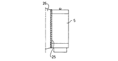
スリーブ2の下端と蓋6との間を気密にするためにカラー17が設けられる。炉の下端は比較的低温であるため、このカラー17は石英材料とすることができる。伸びの差を補償するために、カラー17は支持板10に直接には取り付けられず、突起19を経て空間20内に受け入れられ、ばね21による弾性力下に置かれる。空間20は部分22内に設けられ、この部分は支持板10と蓋6の下方部分との両者に関してシールされ、熱による膨張差を補償する。
【0023】
蓋6は、蓋6を(部分13、12及び15と共に)矢印14の方向で動かすことができるエレベーター軸23に連結される。断熱ブロックの上方に多数の環状の熱遮蔽体12が設けられる。
【0024】
縦型電気炉内のガスの排出又は導入にために導管手段18が設けられる。
【0025】
炉内の温度の計測及び/又は管理のために熱電対11が設けられる。
【0026】
試験中、炉内の温度を1250±0.5℃に維持できることが明らかにされた。炉の長時間使用後においても、内側スリーブ及び支持スリーブの両者とも、その特性は変化しなかった。
【0027】
炉は単独型として示されたが、US−A−5294572に示されたようにクラスター内にこれを導入することが可能である。
【0028】
上述の本発明は本発明の最も好ましい実施例を参照したが、上述された種々の部品に変更を導入することは熟練技術者に明らかでありかつ特許請求の範囲内で可能であることを理解すべきである。
【0029】
本発明の実施態様は次のとおりである。
【0030】
1.支持構造体上に取り付けられたウェーハ処理用の縦型電気炉であって、下端又は上端のいずれかに取外し可能な蓋を有し他方の端部には閉鎖用手段の設けられた内側スリーブ、前記内側スリーブを囲んでいる電気加熱用手段、加熱用手段と内側スリーブとの両者を囲んでいる断熱材及び外側スリーブを備え、内側スリーブは少なくも1200℃の温度に耐える材料よりなりかつ内側スリーブの下方端部において内側スリーブのまわりに配置された支持スリーブの上方部分と係合するための連結用手段が設けられ、前記支持スリーブの下方部分が前記支持構造体上に置かれている縦型電気炉。
【0031】
2.前記内側スリーブがSiC材料よりなる先行実施態様の一つによる炉。
【0032】
3.前記支持スリーブが石英材料よりなる先行実施態様の一つによる炉。
【0033】
4.前記支持構造体が冷却された支持板よりなる先行実施態様の一つによる炉。
【0034】
5.処理すべきウェーハのための受入れ用部材が内側スリーブの内側に設けられ、前記受入れ用部材が前記ウェーハノ装填/取出しのために垂直方向で移動し得る先行実施態様の一つによる炉。
【0035】
6.前記受入れ用部材が熱遮蔽体よりなる先行実施態様の一つによる炉。
【0036】
7.内側スリーブの下端を支持するカラーが設けられ、前記カラーが支持構造体に連結されている先行実施態様の一つによる炉。
【0037】
8.カラー手段と支持構造体との間に温度補償用手段が設けられ、実施態様7と組み合わせた先行実施態様の一つによる縦型電気炉。
【0038】
9.支持構造体上に位置決めされたウェーハ処理用の縦型電気炉であって、下端又は上端のいずれかに取外し可能な蓋を有し他方の端部には閉鎖用手段の設けられた内側スリーブ、前記内側スリーブを囲んでいる電気加熱用手段、加熱用手段と内側スリーブとの両者を囲んでいる断熱体及び外側スリーブを備え、内側スリーブは少なくも1200℃の温度に耐える材料よりなり、内側スリーブの下端と支持構造体との間に石英材料のカラーが設けられた縦型電気炉。
【0039】
10.内側スリーブの下端において内側スリーブのまわりに配置された支持スリーブの上端と組み合うための連結用手段が内側スリーブに設けられ、前記支持スリーブの下端が前記支持構造体上に置かれている実施態様9又は10による炉。11.支持構造体とカラーの取付け具との間に温度補償用手段が設けられる実施態様10による炉。
【図面の簡単な説明】
【図1】本発明の炉の立面図を示す。
【図2】図1による炉の懸架装置を示す。
【図3】図1の詳細を示す。
【符号の説明】
2 内側スリーブ
4 加熱用要素
7 断熱材
8 断熱材
9 支持スリーブ
10 支持板
16 冷却用ダクト
17 カラー[0001]
[Industrial application fields]
The present invention relates to a vertical electric furnace according to the preamble of claim 1 for wafer processing.
[0002]
Such a process must achieve a relatively high temperature with a controlled temperature of the gas atmosphere with relatively high accuracy.
[0003]
[Prior art and its problems]
Recent requirements for processing such wafers require relatively high temperatures. In the present technology, a vertical electric furnace that can be used either alone or in combination with a cluster is known. Such a furnace comprises an inner sleeve, a heating coil, a thermal insulator and an outer sleeve. Usually, the inner sleeve is made of quartz material and rides on a support structure. In most cases, this support structure is cooled.
[0004]
However, when the temperature in the furnace rises to, for example, about 1250 ° C., the quartz material loses luster and deteriorates. The radiation of the heating element provided around the inner sleeve is not transmitted through this sleeve, so that the wafer is not sufficiently heated. Furthermore, this material can become brittle and prone to cracking.
[0005]
Other ceramic materials are known in the art and will withstand high temperatures without degradation of permeation performance. For example, silicon carbide can be used for this purpose.
[0006]
However, the thermal conductivity of such materials is relatively high so that a significant portion of the heat generated in the heating zone will be lost to the support structure. Furthermore, such ceramic materials that withstand relatively high temperatures have a relatively large coefficient of thermal expansion.
[0007]
The present invention aims to provide a furnace that is used at relatively high temperatures, such as about 1200 ° C., and that minimizes heat loss from the inner sleeve to the support structure.
[0008]
[Means for Solving the Problems]
This is achieved according to the invention by the characteristic features of claim 1.
[0009]
According to a preferred embodiment of the invention, the inner sleeve is made of SiC material.
[0010]
The support sleeve is preferably made of a quartz material.
[0011]
The support structure is preferably a cooled support plate.
[0012]
According to a further preferred embodiment, a receiving member for the wafer to be processed is provided inside the inner sleeve, which can be moved in the vertical direction for loading / unloading said wafer.
[0013]
Such receiving member may comprise one or more thermal shields.
[0014]
The lower end of the inner sleeve is preferably supported by a collar made of quartz material.
[0015]
According to yet another preferred embodiment of the present invention, means are provided for compensating for the difference in expansion coefficient, possibly between the inner sleeve material and the support structure material, together with the collar, so as to ensure furnace tightness. Provided.
[0016]
【Example】
Preferred embodiments of the present invention will be shown in more detail with reference to the accompanying drawings.
The furnace shown in the figure has an upper portion that is permanently closed and embodied by the present technology. This furnace can be part of a cluster apparatus according to US-A-5294572. This specification is hereby incorporated by reference.
[0017]
In general, such a furnace comprises an
[0018]
Since SiC is a relatively good heat conductor, when the
[0019]
According to the invention, it is proposed to provide a
[0020]
The position of the support protrusions should be selected such that on the one hand the length of the
[0021]
The support sleeve will convey the weight of the
[0022]
A
[0023]
The lid 6 is connected to an
[0024]
Conduit means 18 are provided for the discharge or introduction of gas in the vertical electric furnace.
[0025]
A
[0026]
During the test, it was found that the temperature in the furnace could be maintained at 1250 ± 0.5 ° C. Even after prolonged use of the furnace, the properties of both the inner sleeve and the support sleeve did not change.
[0027]
Although the furnace was shown as a stand alone, it can be introduced into the cluster as shown in US-A-5294572.
[0028]
Although the above-described invention has referred to the most preferred embodiment of the invention, it will be understood that modifications may be made to the various parts described above which will be apparent to those skilled in the art and are within the scope of the claims. Should.
[0029]
Embodiments of the present invention are as follows.
[0030]
1. A vertical electric furnace for wafer processing mounted on a support structure, having an detachable lid at either the lower end or the upper end, and an inner sleeve provided with closing means at the other end; Means for electric heating surrounding said inner sleeve, heat insulation surrounding both of the means for heating and the inner sleeve and an outer sleeve, the inner sleeve being made of a material capable of withstanding a temperature of at least 1200 ° C. A vertical means provided with connecting means for engaging an upper portion of a support sleeve disposed around the inner sleeve at the lower end of the support sleeve, the lower portion of the support sleeve resting on the support structure Electric furnace.
[0031]
2. A furnace according to one of the preceding embodiments, wherein the inner sleeve is made of SiC material.
[0032]
3. A furnace according to one of the preceding embodiments, wherein the support sleeve is made of quartz material.
[0033]
4). A furnace according to one of the preceding embodiments, wherein the support structure comprises a cooled support plate.
[0034]
5. A furnace according to one of the preceding embodiments, wherein a receiving member for the wafer to be processed is provided inside the inner sleeve, said receiving member being movable in a vertical direction for said wafer loading / unloading.
[0035]
6). A furnace according to one of the preceding embodiments, wherein the receiving member comprises a heat shield.
[0036]
7). A furnace according to one of the previous embodiments, wherein a collar is provided to support the lower end of the inner sleeve, said collar being connected to a support structure.
[0037]
8). A vertical electric furnace according to one of the preceding embodiments, in which temperature compensating means are provided between the collar means and the support structure and combined with embodiment 7.
[0038]
9. A vertical electric furnace for wafer processing positioned on a support structure, which has a removable lid on either the lower end or the upper end and an inner sleeve provided with closing means on the other end; An electric heating means surrounding the inner sleeve, a heat insulator surrounding both the heating means and the inner sleeve, and an outer sleeve, the inner sleeve being made of a material capable of withstanding a temperature of at least 1200 ° C. A vertical electric furnace in which a collar made of quartz material is provided between the lower end of the glass and the support structure.
[0039]
10.
[Brief description of the drawings]
FIG. 1 shows an elevational view of a furnace of the present invention.
2 shows a furnace suspension according to FIG. 1;
FIG. 3 shows details of FIG.
[Explanation of symbols]
2 inner sleeve 4 heating element 7 heat insulating material 8
Claims (2)
Applications Claiming Priority (2)
| Application Number | Priority Date | Filing Date | Title |
|---|---|---|---|
| US414294 | 1995-03-31 | ||
| US08/414,294 US5662470A (en) | 1995-03-31 | 1995-03-31 | Vertical furnace |
Publications (2)
| Publication Number | Publication Date |
|---|---|
| JPH08327238A JPH08327238A (en) | 1996-12-13 |
| JP4285789B2 true JP4285789B2 (en) | 2009-06-24 |
Family
ID=23640837
Family Applications (1)
| Application Number | Title | Priority Date | Filing Date |
|---|---|---|---|
| JP09963396A Expired - Lifetime JP4285789B2 (en) | 1995-03-31 | 1996-03-29 | Vertical electric furnace |
Country Status (7)
| Country | Link |
|---|---|
| US (1) | US5662470A (en) |
| EP (1) | EP0735575B1 (en) |
| JP (1) | JP4285789B2 (en) |
| KR (1) | KR960034959A (en) |
| AT (1) | ATE211583T1 (en) |
| DE (1) | DE69618265T2 (en) |
| TW (1) | TW293082B (en) |
Families Citing this family (255)
| Publication number | Priority date | Publication date | Assignee | Title |
|---|---|---|---|---|
| US5820366A (en) * | 1996-07-10 | 1998-10-13 | Eaton Corporation | Dual vertical thermal processing furnace |
| US6066836A (en) * | 1996-09-23 | 2000-05-23 | Applied Materials, Inc. | High temperature resistive heater for a process chamber |
| NL1005963C2 (en) * | 1997-05-02 | 1998-11-09 | Asm Int | Vertical oven for treating semiconductor substrates. |
| JP3644880B2 (en) * | 2000-06-20 | 2005-05-11 | 東京エレクトロン株式会社 | Vertical heat treatment equipment |
| US6951804B2 (en) * | 2001-02-02 | 2005-10-04 | Applied Materials, Inc. | Formation of a tantalum-nitride layer |
| US6499768B2 (en) * | 2001-05-30 | 2002-12-31 | Asm International N.V. | Joint assembly for connecting two tubes |
| US6746240B2 (en) * | 2002-03-15 | 2004-06-08 | Asm International N.V. | Process tube support sleeve with circumferential channels |
| US6902395B2 (en) * | 2002-03-15 | 2005-06-07 | Asm International, N.V. | Multilevel pedestal for furnace |
| US20070243317A1 (en) * | 2002-07-15 | 2007-10-18 | Du Bois Dale R | Thermal Processing System and Configurable Vertical Chamber |
| JP4523225B2 (en) * | 2002-09-24 | 2010-08-11 | 東京エレクトロン株式会社 | Heat treatment equipment |
| KR100481874B1 (en) * | 2003-02-05 | 2005-04-11 | 삼성전자주식회사 | Diffusion furnace used for manufacturing intergrate circuits and method for cooling the diffusion furnace |
| US7128570B2 (en) * | 2004-01-21 | 2006-10-31 | Asm International N.V. | Method and apparatus for purging seals in a thermal reactor |
| JP4508893B2 (en) * | 2004-02-02 | 2010-07-21 | エーエスエム インターナショナル エヌ.ヴェー. | Semiconductor processing method, semiconductor processing system, and method of supplying gas to reaction chamber |
| US7351057B2 (en) * | 2005-04-27 | 2008-04-01 | Asm International N.V. | Door plate for furnace |
| US7651569B2 (en) * | 2006-02-28 | 2010-01-26 | Asm International N.V. | Pedestal for furnace |
| KR101333363B1 (en) * | 2006-10-13 | 2013-11-28 | 도쿄엘렉트론가부시키가이샤 | Heat treatment apparatus |
| JP4929199B2 (en) * | 2008-02-01 | 2012-05-09 | 株式会社日立国際電気 | Substrate processing apparatus and semiconductor device manufacturing method |
| JP4930438B2 (en) * | 2008-04-03 | 2012-05-16 | 東京エレクトロン株式会社 | Reaction tube and heat treatment equipment |
| JP2009124161A (en) * | 2008-12-26 | 2009-06-04 | Tokyo Electron Ltd | Thermal processing equipment |
| US9394608B2 (en) | 2009-04-06 | 2016-07-19 | Asm America, Inc. | Semiconductor processing reactor and components thereof |
| US8802201B2 (en) | 2009-08-14 | 2014-08-12 | Asm America, Inc. | Systems and methods for thin-film deposition of metal oxides using excited nitrogen-oxygen species |
| CN101969021A (en) * | 2010-08-05 | 2011-02-09 | 北京七星华创电子股份有限公司 | Heat preserving barrel and vertical type heat treatment device with same |
| US20130023129A1 (en) | 2011-07-20 | 2013-01-24 | Asm America, Inc. | Pressure transmitter for a semiconductor processing environment |
| US9017481B1 (en) | 2011-10-28 | 2015-04-28 | Asm America, Inc. | Process feed management for semiconductor substrate processing |
| US10714315B2 (en) | 2012-10-12 | 2020-07-14 | Asm Ip Holdings B.V. | Semiconductor reaction chamber showerhead |
| US20160376700A1 (en) | 2013-02-01 | 2016-12-29 | Asm Ip Holding B.V. | System for treatment of deposition reactor |
| US11015245B2 (en) | 2014-03-19 | 2021-05-25 | Asm Ip Holding B.V. | Gas-phase reactor and system having exhaust plenum and components thereof |
| US10858737B2 (en) | 2014-07-28 | 2020-12-08 | Asm Ip Holding B.V. | Showerhead assembly and components thereof |
| US9890456B2 (en) | 2014-08-21 | 2018-02-13 | Asm Ip Holding B.V. | Method and system for in situ formation of gas-phase compounds |
| US10941490B2 (en) | 2014-10-07 | 2021-03-09 | Asm Ip Holding B.V. | Multiple temperature range susceptor, assembly, reactor and system including the susceptor, and methods of using the same |
| US10276355B2 (en) | 2015-03-12 | 2019-04-30 | Asm Ip Holding B.V. | Multi-zone reactor, system including the reactor, and method of using the same |
| US10458018B2 (en) | 2015-06-26 | 2019-10-29 | Asm Ip Holding B.V. | Structures including metal carbide material, devices including the structures, and methods of forming same |
| US10211308B2 (en) | 2015-10-21 | 2019-02-19 | Asm Ip Holding B.V. | NbMC layers |
| US11139308B2 (en) | 2015-12-29 | 2021-10-05 | Asm Ip Holding B.V. | Atomic layer deposition of III-V compounds to form V-NAND devices |
| US10529554B2 (en) | 2016-02-19 | 2020-01-07 | Asm Ip Holding B.V. | Method for forming silicon nitride film selectively on sidewalls or flat surfaces of trenches |
| US10865475B2 (en) | 2016-04-21 | 2020-12-15 | Asm Ip Holding B.V. | Deposition of metal borides and silicides |
| US10190213B2 (en) | 2016-04-21 | 2019-01-29 | Asm Ip Holding B.V. | Deposition of metal borides |
| US10367080B2 (en) | 2016-05-02 | 2019-07-30 | Asm Ip Holding B.V. | Method of forming a germanium oxynitride film |
| US11453943B2 (en) | 2016-05-25 | 2022-09-27 | Asm Ip Holding B.V. | Method for forming carbon-containing silicon/metal oxide or nitride film by ALD using silicon precursor and hydrocarbon precursor |
| US10612137B2 (en) | 2016-07-08 | 2020-04-07 | Asm Ip Holdings B.V. | Organic reactants for atomic layer deposition |
| US9859151B1 (en) | 2016-07-08 | 2018-01-02 | Asm Ip Holding B.V. | Selective film deposition method to form air gaps |
| US9812320B1 (en) | 2016-07-28 | 2017-11-07 | Asm Ip Holding B.V. | Method and apparatus for filling a gap |
| KR102532607B1 (en) | 2016-07-28 | 2023-05-15 | 에이에스엠 아이피 홀딩 비.브이. | Substrate processing apparatus and method of operating the same |
| US9887082B1 (en) | 2016-07-28 | 2018-02-06 | Asm Ip Holding B.V. | Method and apparatus for filling a gap |
| US10643826B2 (en) | 2016-10-26 | 2020-05-05 | Asm Ip Holdings B.V. | Methods for thermally calibrating reaction chambers |
| US11532757B2 (en) | 2016-10-27 | 2022-12-20 | Asm Ip Holding B.V. | Deposition of charge trapping layers |
| US10229833B2 (en) | 2016-11-01 | 2019-03-12 | Asm Ip Holding B.V. | Methods for forming a transition metal nitride film on a substrate by atomic layer deposition and related semiconductor device structures |
| US10714350B2 (en) | 2016-11-01 | 2020-07-14 | ASM IP Holdings, B.V. | Methods for forming a transition metal niobium nitride film on a substrate by atomic layer deposition and related semiconductor device structures |
| KR102546317B1 (en) | 2016-11-15 | 2023-06-21 | 에이에스엠 아이피 홀딩 비.브이. | Gas supply unit and substrate processing apparatus including the same |
| KR20180068582A (en) | 2016-12-14 | 2018-06-22 | 에이에스엠 아이피 홀딩 비.브이. | Substrate processing apparatus |
| US11447861B2 (en) | 2016-12-15 | 2022-09-20 | Asm Ip Holding B.V. | Sequential infiltration synthesis apparatus and a method of forming a patterned structure |
| US11581186B2 (en) | 2016-12-15 | 2023-02-14 | Asm Ip Holding B.V. | Sequential infiltration synthesis apparatus |
| KR20180070971A (en) | 2016-12-19 | 2018-06-27 | 에이에스엠 아이피 홀딩 비.브이. | Substrate processing apparatus |
| US10269558B2 (en) | 2016-12-22 | 2019-04-23 | Asm Ip Holding B.V. | Method of forming a structure on a substrate |
| US10867788B2 (en) | 2016-12-28 | 2020-12-15 | Asm Ip Holding B.V. | Method of forming a structure on a substrate |
| US11390950B2 (en) | 2017-01-10 | 2022-07-19 | Asm Ip Holding B.V. | Reactor system and method to reduce residue buildup during a film deposition process |
| US10468261B2 (en) | 2017-02-15 | 2019-11-05 | Asm Ip Holding B.V. | Methods for forming a metallic film on a substrate by cyclical deposition and related semiconductor device structures |
| US10529563B2 (en) | 2017-03-29 | 2020-01-07 | Asm Ip Holdings B.V. | Method for forming doped metal oxide films on a substrate by cyclical deposition and related semiconductor device structures |
| KR102457289B1 (en) | 2017-04-25 | 2022-10-21 | 에이에스엠 아이피 홀딩 비.브이. | Method for depositing a thin film and manufacturing a semiconductor device |
| US10770286B2 (en) | 2017-05-08 | 2020-09-08 | Asm Ip Holdings B.V. | Methods for selectively forming a silicon nitride film on a substrate and related semiconductor device structures |
| US10892156B2 (en) | 2017-05-08 | 2021-01-12 | Asm Ip Holding B.V. | Methods for forming a silicon nitride film on a substrate and related semiconductor device structures |
| US10886123B2 (en) | 2017-06-02 | 2021-01-05 | Asm Ip Holding B.V. | Methods for forming low temperature semiconductor layers and related semiconductor device structures |
| US11306395B2 (en) | 2017-06-28 | 2022-04-19 | Asm Ip Holding B.V. | Methods for depositing a transition metal nitride film on a substrate by atomic layer deposition and related deposition apparatus |
| KR20190009245A (en) | 2017-07-18 | 2019-01-28 | 에이에스엠 아이피 홀딩 비.브이. | Methods for forming a semiconductor device structure and related semiconductor device structures |
| US10541333B2 (en) | 2017-07-19 | 2020-01-21 | Asm Ip Holding B.V. | Method for depositing a group IV semiconductor and related semiconductor device structures |
| US11018002B2 (en) | 2017-07-19 | 2021-05-25 | Asm Ip Holding B.V. | Method for selectively depositing a Group IV semiconductor and related semiconductor device structures |
| US11374112B2 (en) | 2017-07-19 | 2022-06-28 | Asm Ip Holding B.V. | Method for depositing a group IV semiconductor and related semiconductor device structures |
| US10590535B2 (en) | 2017-07-26 | 2020-03-17 | Asm Ip Holdings B.V. | Chemical treatment, deposition and/or infiltration apparatus and method for using the same |
| US10770336B2 (en) | 2017-08-08 | 2020-09-08 | Asm Ip Holding B.V. | Substrate lift mechanism and reactor including same |
| US10692741B2 (en) | 2017-08-08 | 2020-06-23 | Asm Ip Holdings B.V. | Radiation shield |
| US11139191B2 (en) | 2017-08-09 | 2021-10-05 | Asm Ip Holding B.V. | Storage apparatus for storing cassettes for substrates and processing apparatus equipped therewith |
| US11769682B2 (en) | 2017-08-09 | 2023-09-26 | Asm Ip Holding B.V. | Storage apparatus for storing cassettes for substrates and processing apparatus equipped therewith |
| US11830730B2 (en) | 2017-08-29 | 2023-11-28 | Asm Ip Holding B.V. | Layer forming method and apparatus |
| US11295980B2 (en) | 2017-08-30 | 2022-04-05 | Asm Ip Holding B.V. | Methods for depositing a molybdenum metal film over a dielectric surface of a substrate by a cyclical deposition process and related semiconductor device structures |
| KR102491945B1 (en) | 2017-08-30 | 2023-01-26 | 에이에스엠 아이피 홀딩 비.브이. | Substrate processing apparatus |
| US11056344B2 (en) | 2017-08-30 | 2021-07-06 | Asm Ip Holding B.V. | Layer forming method |
| KR102630301B1 (en) | 2017-09-21 | 2024-01-29 | 에이에스엠 아이피 홀딩 비.브이. | Method of sequential infiltration synthesis treatment of infiltrateable material and structures and devices formed using same |
| US10844484B2 (en) | 2017-09-22 | 2020-11-24 | Asm Ip Holding B.V. | Apparatus for dispensing a vapor phase reactant to a reaction chamber and related methods |
| US10658205B2 (en) | 2017-09-28 | 2020-05-19 | Asm Ip Holdings B.V. | Chemical dispensing apparatus and methods for dispensing a chemical to a reaction chamber |
| US10403504B2 (en) | 2017-10-05 | 2019-09-03 | Asm Ip Holding B.V. | Method for selectively depositing a metallic film on a substrate |
| US10923344B2 (en) | 2017-10-30 | 2021-02-16 | Asm Ip Holding B.V. | Methods for forming a semiconductor structure and related semiconductor structures |
| US10910262B2 (en) | 2017-11-16 | 2021-02-02 | Asm Ip Holding B.V. | Method of selectively depositing a capping layer structure on a semiconductor device structure |
| US11022879B2 (en) | 2017-11-24 | 2021-06-01 | Asm Ip Holding B.V. | Method of forming an enhanced unexposed photoresist layer |
| JP7214724B2 (en) | 2017-11-27 | 2023-01-30 | エーエスエム アイピー ホールディング ビー.ブイ. | Storage device for storing wafer cassettes used in batch furnaces |
| TWI791689B (en) | 2017-11-27 | 2023-02-11 | 荷蘭商Asm智慧財產控股私人有限公司 | Apparatus including a clean mini environment |
| US10872771B2 (en) | 2018-01-16 | 2020-12-22 | Asm Ip Holding B. V. | Method for depositing a material film on a substrate within a reaction chamber by a cyclical deposition process and related device structures |
| CN111630203A (en) | 2018-01-19 | 2020-09-04 | Asm Ip私人控股有限公司 | Method for depositing gap filling layer by plasma auxiliary deposition |
| TW202325889A (en) | 2018-01-19 | 2023-07-01 | 荷蘭商Asm 智慧財產控股公司 | Deposition method |
| US11018047B2 (en) | 2018-01-25 | 2021-05-25 | Asm Ip Holding B.V. | Hybrid lift pin |
| USD880437S1 (en) | 2018-02-01 | 2020-04-07 | Asm Ip Holding B.V. | Gas supply plate for semiconductor manufacturing apparatus |
| US11081345B2 (en) | 2018-02-06 | 2021-08-03 | Asm Ip Holding B.V. | Method of post-deposition treatment for silicon oxide film |
| JP7124098B2 (en) | 2018-02-14 | 2022-08-23 | エーエスエム・アイピー・ホールディング・ベー・フェー | Method for depositing a ruthenium-containing film on a substrate by a cyclical deposition process |
| US10896820B2 (en) | 2018-02-14 | 2021-01-19 | Asm Ip Holding B.V. | Method for depositing a ruthenium-containing film on a substrate by a cyclical deposition process |
| KR102636427B1 (en) | 2018-02-20 | 2024-02-13 | 에이에스엠 아이피 홀딩 비.브이. | Substrate processing method and apparatus |
| US10975470B2 (en) | 2018-02-23 | 2021-04-13 | Asm Ip Holding B.V. | Apparatus for detecting or monitoring for a chemical precursor in a high temperature environment |
| US11473195B2 (en) | 2018-03-01 | 2022-10-18 | Asm Ip Holding B.V. | Semiconductor processing apparatus and a method for processing a substrate |
| US11629406B2 (en) | 2018-03-09 | 2023-04-18 | Asm Ip Holding B.V. | Semiconductor processing apparatus comprising one or more pyrometers for measuring a temperature of a substrate during transfer of the substrate |
| US11114283B2 (en) | 2018-03-16 | 2021-09-07 | Asm Ip Holding B.V. | Reactor, system including the reactor, and methods of manufacturing and using same |
| KR102646467B1 (en) | 2018-03-27 | 2024-03-11 | 에이에스엠 아이피 홀딩 비.브이. | Method of forming an electrode on a substrate and a semiconductor device structure including an electrode |
| US11088002B2 (en) | 2018-03-29 | 2021-08-10 | Asm Ip Holding B.V. | Substrate rack and a substrate processing system and method |
| US11230766B2 (en) | 2018-03-29 | 2022-01-25 | Asm Ip Holding B.V. | Substrate processing apparatus and method |
| KR102501472B1 (en) | 2018-03-30 | 2023-02-20 | 에이에스엠 아이피 홀딩 비.브이. | Substrate processing method |
| KR20190128558A (en) | 2018-05-08 | 2019-11-18 | 에이에스엠 아이피 홀딩 비.브이. | Methods for depositing an oxide film on a substrate by a cyclical deposition process and related device structures |
| TW202349473A (en) | 2018-05-11 | 2023-12-16 | 荷蘭商Asm Ip私人控股有限公司 | Methods for forming a doped metal carbide film on a substrate and related semiconductor device structures |
| KR102596988B1 (en) | 2018-05-28 | 2023-10-31 | 에이에스엠 아이피 홀딩 비.브이. | Method of processing a substrate and a device manufactured by the same |
| US11718913B2 (en) | 2018-06-04 | 2023-08-08 | Asm Ip Holding B.V. | Gas distribution system and reactor system including same |
| US11270899B2 (en) | 2018-06-04 | 2022-03-08 | Asm Ip Holding B.V. | Wafer handling chamber with moisture reduction |
| US11286562B2 (en) | 2018-06-08 | 2022-03-29 | Asm Ip Holding B.V. | Gas-phase chemical reactor and method of using same |
| KR102568797B1 (en) | 2018-06-21 | 2023-08-21 | 에이에스엠 아이피 홀딩 비.브이. | Substrate processing system |
| US10797133B2 (en) | 2018-06-21 | 2020-10-06 | Asm Ip Holding B.V. | Method for depositing a phosphorus doped silicon arsenide film and related semiconductor device structures |
| CN112292478A (en) | 2018-06-27 | 2021-01-29 | Asm Ip私人控股有限公司 | Cyclic deposition methods for forming metal-containing materials and films and structures containing metal-containing materials |
| WO2020003000A1 (en) | 2018-06-27 | 2020-01-02 | Asm Ip Holding B.V. | Cyclic deposition methods for forming metal-containing material and films and structures including the metal-containing material |
| US10612136B2 (en) | 2018-06-29 | 2020-04-07 | ASM IP Holding, B.V. | Temperature-controlled flange and reactor system including same |
| KR20200002519A (en) | 2018-06-29 | 2020-01-08 | 에이에스엠 아이피 홀딩 비.브이. | Method for depositing a thin film and manufacturing a semiconductor device |
| US10755922B2 (en) | 2018-07-03 | 2020-08-25 | Asm Ip Holding B.V. | Method for depositing silicon-free carbon-containing film as gap-fill layer by pulse plasma-assisted deposition |
| US10388513B1 (en) | 2018-07-03 | 2019-08-20 | Asm Ip Holding B.V. | Method for depositing silicon-free carbon-containing film as gap-fill layer by pulse plasma-assisted deposition |
| US10767789B2 (en) | 2018-07-16 | 2020-09-08 | Asm Ip Holding B.V. | Diaphragm valves, valve components, and methods for forming valve components |
| US11053591B2 (en) | 2018-08-06 | 2021-07-06 | Asm Ip Holding B.V. | Multi-port gas injection system and reactor system including same |
| US10883175B2 (en) | 2018-08-09 | 2021-01-05 | Asm Ip Holding B.V. | Vertical furnace for processing substrates and a liner for use therein |
| US10829852B2 (en) | 2018-08-16 | 2020-11-10 | Asm Ip Holding B.V. | Gas distribution device for a wafer processing apparatus |
| US11430674B2 (en) | 2018-08-22 | 2022-08-30 | Asm Ip Holding B.V. | Sensor array, apparatus for dispensing a vapor phase reactant to a reaction chamber and related methods |
| KR20200030162A (en) | 2018-09-11 | 2020-03-20 | 에이에스엠 아이피 홀딩 비.브이. | Method for deposition of a thin film |
| US11024523B2 (en) | 2018-09-11 | 2021-06-01 | Asm Ip Holding B.V. | Substrate processing apparatus and method |
| US11049751B2 (en) | 2018-09-14 | 2021-06-29 | Asm Ip Holding B.V. | Cassette supply system to store and handle cassettes and processing apparatus equipped therewith |
| CN110970344A (en) | 2018-10-01 | 2020-04-07 | Asm Ip控股有限公司 | Substrate holding apparatus, system including the same, and method of using the same |
| US11232963B2 (en) | 2018-10-03 | 2022-01-25 | Asm Ip Holding B.V. | Substrate processing apparatus and method |
| KR102592699B1 (en) | 2018-10-08 | 2023-10-23 | 에이에스엠 아이피 홀딩 비.브이. | Substrate support unit and apparatuses for depositing thin film and processing the substrate including the same |
| KR102605121B1 (en) | 2018-10-19 | 2023-11-23 | 에이에스엠 아이피 홀딩 비.브이. | Substrate processing apparatus and substrate processing method |
| KR102546322B1 (en) | 2018-10-19 | 2023-06-21 | 에이에스엠 아이피 홀딩 비.브이. | Substrate processing apparatus and substrate processing method |
| USD948463S1 (en) | 2018-10-24 | 2022-04-12 | Asm Ip Holding B.V. | Susceptor for semiconductor substrate supporting apparatus |
| US11087997B2 (en) | 2018-10-31 | 2021-08-10 | Asm Ip Holding B.V. | Substrate processing apparatus for processing substrates |
| KR20200051105A (en) | 2018-11-02 | 2020-05-13 | 에이에스엠 아이피 홀딩 비.브이. | Substrate support unit and substrate processing apparatus including the same |
| US11572620B2 (en) | 2018-11-06 | 2023-02-07 | Asm Ip Holding B.V. | Methods for selectively depositing an amorphous silicon film on a substrate |
| US11031242B2 (en) | 2018-11-07 | 2021-06-08 | Asm Ip Holding B.V. | Methods for depositing a boron doped silicon germanium film |
| US10847366B2 (en) | 2018-11-16 | 2020-11-24 | Asm Ip Holding B.V. | Methods for depositing a transition metal chalcogenide film on a substrate by a cyclical deposition process |
| US10818758B2 (en) | 2018-11-16 | 2020-10-27 | Asm Ip Holding B.V. | Methods for forming a metal silicate film on a substrate in a reaction chamber and related semiconductor device structures |
| US11217444B2 (en) | 2018-11-30 | 2022-01-04 | Asm Ip Holding B.V. | Method for forming an ultraviolet radiation responsive metal oxide-containing film |
| KR102636428B1 (en) | 2018-12-04 | 2024-02-13 | 에이에스엠 아이피 홀딩 비.브이. | A method for cleaning a substrate processing apparatus |
| US11158513B2 (en) | 2018-12-13 | 2021-10-26 | Asm Ip Holding B.V. | Methods for forming a rhenium-containing film on a substrate by a cyclical deposition process and related semiconductor device structures |
| JP2020096183A (en) | 2018-12-14 | 2020-06-18 | エーエスエム・アイピー・ホールディング・ベー・フェー | Method of forming device structure using selective deposition of gallium nitride, and system for the same |
| TWI819180B (en) | 2019-01-17 | 2023-10-21 | 荷蘭商Asm 智慧財產控股公司 | Methods of forming a transition metal containing film on a substrate by a cyclical deposition process |
| KR20200091543A (en) | 2019-01-22 | 2020-07-31 | 에이에스엠 아이피 홀딩 비.브이. | Semiconductor processing device |
| CN111524788B (en) | 2019-02-01 | 2023-11-24 | Asm Ip私人控股有限公司 | Method for topologically selective film formation of silicon oxide |
| TW202044325A (en) | 2019-02-20 | 2020-12-01 | 荷蘭商Asm Ip私人控股有限公司 | Method of filling a recess formed within a surface of a substrate, semiconductor structure formed according to the method, and semiconductor processing apparatus |
| KR20200102357A (en) | 2019-02-20 | 2020-08-31 | 에이에스엠 아이피 홀딩 비.브이. | Apparatus and methods for plug fill deposition in 3-d nand applications |
| TW202104632A (en) | 2019-02-20 | 2021-02-01 | 荷蘭商Asm Ip私人控股有限公司 | Cyclical deposition method and apparatus for filling a recess formed within a substrate surface |
| KR102626263B1 (en) | 2019-02-20 | 2024-01-16 | 에이에스엠 아이피 홀딩 비.브이. | Cyclical deposition method including treatment step and apparatus for same |
| TW202100794A (en) | 2019-02-22 | 2021-01-01 | 荷蘭商Asm Ip私人控股有限公司 | Substrate processing apparatus and method for processing substrate |
| KR20200108242A (en) | 2019-03-08 | 2020-09-17 | 에이에스엠 아이피 홀딩 비.브이. | Method for Selective Deposition of Silicon Nitride Layer and Structure Including Selectively-Deposited Silicon Nitride Layer |
| US11742198B2 (en) | 2019-03-08 | 2023-08-29 | Asm Ip Holding B.V. | Structure including SiOCN layer and method of forming same |
| KR20200108243A (en) | 2019-03-08 | 2020-09-17 | 에이에스엠 아이피 홀딩 비.브이. | Structure Including SiOC Layer and Method of Forming Same |
| KR20200116033A (en) | 2019-03-28 | 2020-10-08 | 에이에스엠 아이피 홀딩 비.브이. | Door opener and substrate processing apparatus provided therewith |
| KR20200116855A (en) | 2019-04-01 | 2020-10-13 | 에이에스엠 아이피 홀딩 비.브이. | Method of manufacturing semiconductor device |
| KR20200123380A (en) | 2019-04-19 | 2020-10-29 | 에이에스엠 아이피 홀딩 비.브이. | Layer forming method and apparatus |
| KR20200125453A (en) | 2019-04-24 | 2020-11-04 | 에이에스엠 아이피 홀딩 비.브이. | Gas-phase reactor system and method of using same |
| KR20200130118A (en) | 2019-05-07 | 2020-11-18 | 에이에스엠 아이피 홀딩 비.브이. | Method for Reforming Amorphous Carbon Polymer Film |
| KR20200130121A (en) | 2019-05-07 | 2020-11-18 | 에이에스엠 아이피 홀딩 비.브이. | Chemical source vessel with dip tube |
| KR20200130652A (en) | 2019-05-10 | 2020-11-19 | 에이에스엠 아이피 홀딩 비.브이. | Method of depositing material onto a surface and structure formed according to the method |
| JP2020188255A (en) | 2019-05-16 | 2020-11-19 | エーエスエム アイピー ホールディング ビー.ブイ. | Wafer boat handling device, vertical batch furnace, and method |
| USD975665S1 (en) | 2019-05-17 | 2023-01-17 | Asm Ip Holding B.V. | Susceptor shaft |
| USD947913S1 (en) | 2019-05-17 | 2022-04-05 | Asm Ip Holding B.V. | Susceptor shaft |
| USD935572S1 (en) | 2019-05-24 | 2021-11-09 | Asm Ip Holding B.V. | Gas channel plate |
| USD922229S1 (en) | 2019-06-05 | 2021-06-15 | Asm Ip Holding B.V. | Device for controlling a temperature of a gas supply unit |
| KR20200141003A (en) | 2019-06-06 | 2020-12-17 | 에이에스엠 아이피 홀딩 비.브이. | Gas-phase reactor system including a gas detector |
| KR20200143254A (en) | 2019-06-11 | 2020-12-23 | 에이에스엠 아이피 홀딩 비.브이. | Method of forming an electronic structure using an reforming gas, system for performing the method, and structure formed using the method |
| USD944946S1 (en) | 2019-06-14 | 2022-03-01 | Asm Ip Holding B.V. | Shower plate |
| USD931978S1 (en) | 2019-06-27 | 2021-09-28 | Asm Ip Holding B.V. | Showerhead vacuum transport |
| KR20210005515A (en) | 2019-07-03 | 2021-01-14 | 에이에스엠 아이피 홀딩 비.브이. | Temperature control assembly for substrate processing apparatus and method of using same |
| JP2021015791A (en) | 2019-07-09 | 2021-02-12 | エーエスエム アイピー ホールディング ビー.ブイ. | Plasma device and substrate processing method using coaxial waveguide |
| CN112216646A (en) | 2019-07-10 | 2021-01-12 | Asm Ip私人控股有限公司 | Substrate supporting assembly and substrate processing device comprising same |
| KR20210010307A (en) | 2019-07-16 | 2021-01-27 | 에이에스엠 아이피 홀딩 비.브이. | Substrate processing apparatus |
| KR20210010820A (en) | 2019-07-17 | 2021-01-28 | 에이에스엠 아이피 홀딩 비.브이. | Methods of forming silicon germanium structures |
| KR20210010816A (en) | 2019-07-17 | 2021-01-28 | 에이에스엠 아이피 홀딩 비.브이. | Radical assist ignition plasma system and method |
| US11643724B2 (en) | 2019-07-18 | 2023-05-09 | Asm Ip Holding B.V. | Method of forming structures using a neutral beam |
| CN112242296A (en) | 2019-07-19 | 2021-01-19 | Asm Ip私人控股有限公司 | Method of forming topologically controlled amorphous carbon polymer films |
| TW202113936A (en) | 2019-07-29 | 2021-04-01 | 荷蘭商Asm Ip私人控股有限公司 | Methods for selective deposition utilizing n-type dopants and/or alternative dopants to achieve high dopant incorporation |
| CN112309899A (en) | 2019-07-30 | 2021-02-02 | Asm Ip私人控股有限公司 | Substrate processing apparatus |
| CN112309900A (en) | 2019-07-30 | 2021-02-02 | Asm Ip私人控股有限公司 | Substrate processing apparatus |
| US11227782B2 (en) | 2019-07-31 | 2022-01-18 | Asm Ip Holding B.V. | Vertical batch furnace assembly |
| US11587814B2 (en) | 2019-07-31 | 2023-02-21 | Asm Ip Holding B.V. | Vertical batch furnace assembly |
| US11587815B2 (en) | 2019-07-31 | 2023-02-21 | Asm Ip Holding B.V. | Vertical batch furnace assembly |
| CN112323048B (en) | 2019-08-05 | 2024-02-09 | Asm Ip私人控股有限公司 | Liquid level sensor for chemical source container |
| USD965044S1 (en) | 2019-08-19 | 2022-09-27 | Asm Ip Holding B.V. | Susceptor shaft |
| USD965524S1 (en) | 2019-08-19 | 2022-10-04 | Asm Ip Holding B.V. | Susceptor support |
| JP2021031769A (en) | 2019-08-21 | 2021-03-01 | エーエスエム アイピー ホールディング ビー.ブイ. | Production apparatus of mixed gas of film deposition raw material and film deposition apparatus |
| USD940837S1 (en) | 2019-08-22 | 2022-01-11 | Asm Ip Holding B.V. | Electrode |
| USD930782S1 (en) | 2019-08-22 | 2021-09-14 | Asm Ip Holding B.V. | Gas distributor |
| KR20210024423A (en) | 2019-08-22 | 2021-03-05 | 에이에스엠 아이피 홀딩 비.브이. | Method for forming a structure with a hole |
| USD949319S1 (en) | 2019-08-22 | 2022-04-19 | Asm Ip Holding B.V. | Exhaust duct |
| USD979506S1 (en) | 2019-08-22 | 2023-02-28 | Asm Ip Holding B.V. | Insulator |
| KR20210024420A (en) | 2019-08-23 | 2021-03-05 | 에이에스엠 아이피 홀딩 비.브이. | Method for depositing silicon oxide film having improved quality by peald using bis(diethylamino)silane |
| US11286558B2 (en) | 2019-08-23 | 2022-03-29 | Asm Ip Holding B.V. | Methods for depositing a molybdenum nitride film on a surface of a substrate by a cyclical deposition process and related semiconductor device structures including a molybdenum nitride film |
| KR20210029090A (en) | 2019-09-04 | 2021-03-15 | 에이에스엠 아이피 홀딩 비.브이. | Methods for selective deposition using a sacrificial capping layer |
| KR20210029663A (en) | 2019-09-05 | 2021-03-16 | 에이에스엠 아이피 홀딩 비.브이. | Substrate processing apparatus |
| US11562901B2 (en) | 2019-09-25 | 2023-01-24 | Asm Ip Holding B.V. | Substrate processing method |
| CN112593212B (en) | 2019-10-02 | 2023-12-22 | Asm Ip私人控股有限公司 | Method for forming topologically selective silicon oxide film by cyclic plasma enhanced deposition process |
| TW202129060A (en) | 2019-10-08 | 2021-08-01 | 荷蘭商Asm Ip控股公司 | Substrate processing device, and substrate processing method |
| KR20210043460A (en) | 2019-10-10 | 2021-04-21 | 에이에스엠 아이피 홀딩 비.브이. | Method of forming a photoresist underlayer and structure including same |
| KR20210045930A (en) | 2019-10-16 | 2021-04-27 | 에이에스엠 아이피 홀딩 비.브이. | Method of Topology-Selective Film Formation of Silicon Oxide |
| US11637014B2 (en) | 2019-10-17 | 2023-04-25 | Asm Ip Holding B.V. | Methods for selective deposition of doped semiconductor material |
| KR20210047808A (en) | 2019-10-21 | 2021-04-30 | 에이에스엠 아이피 홀딩 비.브이. | Apparatus and methods for selectively etching films |
| US11646205B2 (en) | 2019-10-29 | 2023-05-09 | Asm Ip Holding B.V. | Methods of selectively forming n-type doped material on a surface, systems for selectively forming n-type doped material, and structures formed using same |
| KR20210054983A (en) | 2019-11-05 | 2021-05-14 | 에이에스엠 아이피 홀딩 비.브이. | Structures with doped semiconductor layers and methods and systems for forming same |
| US11501968B2 (en) | 2019-11-15 | 2022-11-15 | Asm Ip Holding B.V. | Method for providing a semiconductor device with silicon filled gaps |
| KR20210062561A (en) | 2019-11-20 | 2021-05-31 | 에이에스엠 아이피 홀딩 비.브이. | Method of depositing carbon-containing material on a surface of a substrate, structure formed using the method, and system for forming the structure |
| CN112951697A (en) | 2019-11-26 | 2021-06-11 | Asm Ip私人控股有限公司 | Substrate processing apparatus |
| US11450529B2 (en) | 2019-11-26 | 2022-09-20 | Asm Ip Holding B.V. | Methods for selectively forming a target film on a substrate comprising a first dielectric surface and a second metallic surface |
| CN112885692A (en) | 2019-11-29 | 2021-06-01 | Asm Ip私人控股有限公司 | Substrate processing apparatus |
| CN112885693A (en) | 2019-11-29 | 2021-06-01 | Asm Ip私人控股有限公司 | Substrate processing apparatus |
| JP2021090042A (en) | 2019-12-02 | 2021-06-10 | エーエスエム アイピー ホールディング ビー.ブイ. | Substrate processing apparatus and substrate processing method |
| KR20210070898A (en) | 2019-12-04 | 2021-06-15 | 에이에스엠 아이피 홀딩 비.브이. | Substrate processing apparatus |
| US11885013B2 (en) | 2019-12-17 | 2024-01-30 | Asm Ip Holding B.V. | Method of forming vanadium nitride layer and structure including the vanadium nitride layer |
| KR20210080214A (en) | 2019-12-19 | 2021-06-30 | 에이에스엠 아이피 홀딩 비.브이. | Methods for filling a gap feature on a substrate and related semiconductor structures |
| KR20210095050A (en) | 2020-01-20 | 2021-07-30 | 에이에스엠 아이피 홀딩 비.브이. | Method of forming thin film and method of modifying surface of thin film |
| TW202130846A (en) | 2020-02-03 | 2021-08-16 | 荷蘭商Asm Ip私人控股有限公司 | Method of forming structures including a vanadium or indium layer |
| TW202146882A (en) | 2020-02-04 | 2021-12-16 | 荷蘭商Asm Ip私人控股有限公司 | Method of verifying an article, apparatus for verifying an article, and system for verifying a reaction chamber |
| US11776846B2 (en) | 2020-02-07 | 2023-10-03 | Asm Ip Holding B.V. | Methods for depositing gap filling fluids and related systems and devices |
| TW202146715A (en) | 2020-02-17 | 2021-12-16 | 荷蘭商Asm Ip私人控股有限公司 | Method for growing phosphorous-doped silicon layer and system of the same |
| US11444053B2 (en) | 2020-02-25 | 2022-09-13 | Yield Engineering Systems, Inc. | Batch processing oven and method |
| KR20210116249A (en) | 2020-03-11 | 2021-09-27 | 에이에스엠 아이피 홀딩 비.브이. | lockout tagout assembly and system and method of using same |
| KR20210116240A (en) | 2020-03-11 | 2021-09-27 | 에이에스엠 아이피 홀딩 비.브이. | Substrate handling device with adjustable joints |
| KR20210117157A (en) | 2020-03-12 | 2021-09-28 | 에이에스엠 아이피 홀딩 비.브이. | Method for Fabricating Layer Structure Having Target Topological Profile |
| KR20210124042A (en) | 2020-04-02 | 2021-10-14 | 에이에스엠 아이피 홀딩 비.브이. | Thin film forming method |
| TW202146689A (en) | 2020-04-03 | 2021-12-16 | 荷蘭商Asm Ip控股公司 | Method for forming barrier layer and method for manufacturing semiconductor device |
| TW202145344A (en) | 2020-04-08 | 2021-12-01 | 荷蘭商Asm Ip私人控股有限公司 | Apparatus and methods for selectively etching silcon oxide films |
| US11821078B2 (en) | 2020-04-15 | 2023-11-21 | Asm Ip Holding B.V. | Method for forming precoat film and method for forming silicon-containing film |
| KR20210132605A (en) | 2020-04-24 | 2021-11-04 | 에이에스엠 아이피 홀딩 비.브이. | Vertical batch furnace assembly comprising a cooling gas supply |
| CN113555279A (en) | 2020-04-24 | 2021-10-26 | Asm Ip私人控股有限公司 | Method of forming vanadium nitride-containing layers and structures including the same |
| KR20210132600A (en) | 2020-04-24 | 2021-11-04 | 에이에스엠 아이피 홀딩 비.브이. | Methods and systems for depositing a layer comprising vanadium, nitrogen, and a further element |
| KR20210134226A (en) | 2020-04-29 | 2021-11-09 | 에이에스엠 아이피 홀딩 비.브이. | Solid source precursor vessel |
| KR20210134869A (en) | 2020-05-01 | 2021-11-11 | 에이에스엠 아이피 홀딩 비.브이. | Fast FOUP swapping with a FOUP handler |
| KR20210141379A (en) | 2020-05-13 | 2021-11-23 | 에이에스엠 아이피 홀딩 비.브이. | Laser alignment fixture for a reactor system |
| KR20210143653A (en) | 2020-05-19 | 2021-11-29 | 에이에스엠 아이피 홀딩 비.브이. | Substrate processing apparatus |
| KR20210145078A (en) | 2020-05-21 | 2021-12-01 | 에이에스엠 아이피 홀딩 비.브이. | Structures including multiple carbon layers and methods of forming and using same |
| TW202201602A (en) | 2020-05-29 | 2022-01-01 | 荷蘭商Asm Ip私人控股有限公司 | Substrate processing device |
| TW202218133A (en) | 2020-06-24 | 2022-05-01 | 荷蘭商Asm Ip私人控股有限公司 | Method for forming a layer provided with silicon |
| TW202217953A (en) | 2020-06-30 | 2022-05-01 | 荷蘭商Asm Ip私人控股有限公司 | Substrate processing method |
| US11699602B2 (en) * | 2020-07-07 | 2023-07-11 | Applied Materials, Inc. | Substrate support assemblies and components |
| KR20220010438A (en) | 2020-07-17 | 2022-01-25 | 에이에스엠 아이피 홀딩 비.브이. | Structures and methods for use in photolithography |
| TW202204662A (en) | 2020-07-20 | 2022-02-01 | 荷蘭商Asm Ip私人控股有限公司 | Method and system for depositing molybdenum layers |
| TW202212623A (en) | 2020-08-26 | 2022-04-01 | 荷蘭商Asm Ip私人控股有限公司 | Method of forming metal silicon oxide layer and metal silicon oxynitride layer, semiconductor structure, and system |
| USD990534S1 (en) | 2020-09-11 | 2023-06-27 | Asm Ip Holding B.V. | Weighted lift pin |
| USD1012873S1 (en) | 2020-09-24 | 2024-01-30 | Asm Ip Holding B.V. | Electrode for semiconductor processing apparatus |
| TW202229613A (en) | 2020-10-14 | 2022-08-01 | 荷蘭商Asm Ip私人控股有限公司 | Method of depositing material on stepped structure |
| TW202217037A (en) | 2020-10-22 | 2022-05-01 | 荷蘭商Asm Ip私人控股有限公司 | Method of depositing vanadium metal, structure, device and a deposition assembly |
| TW202223136A (en) | 2020-10-28 | 2022-06-16 | 荷蘭商Asm Ip私人控股有限公司 | Method for forming layer on substrate, and semiconductor processing system |
| KR20220076343A (en) | 2020-11-30 | 2022-06-08 | 에이에스엠 아이피 홀딩 비.브이. | an injector configured for arrangement within a reaction chamber of a substrate processing apparatus |
| US11688621B2 (en) | 2020-12-10 | 2023-06-27 | Yield Engineering Systems, Inc. | Batch processing oven and operating methods |
| US11946137B2 (en) | 2020-12-16 | 2024-04-02 | Asm Ip Holding B.V. | Runout and wobble measurement fixtures |
| TW202231903A (en) | 2020-12-22 | 2022-08-16 | 荷蘭商Asm Ip私人控股有限公司 | Transition metal deposition method, transition metal layer, and deposition assembly for depositing transition metal on substrate |
| USD980814S1 (en) | 2021-05-11 | 2023-03-14 | Asm Ip Holding B.V. | Gas distributor for substrate processing apparatus |
| USD981973S1 (en) | 2021-05-11 | 2023-03-28 | Asm Ip Holding B.V. | Reactor wall for substrate processing apparatus |
| USD980813S1 (en) | 2021-05-11 | 2023-03-14 | Asm Ip Holding B.V. | Gas flow control plate for substrate processing apparatus |
| USD1023959S1 (en) | 2021-05-11 | 2024-04-23 | Asm Ip Holding B.V. | Electrode for substrate processing apparatus |
| USD990441S1 (en) | 2021-09-07 | 2023-06-27 | Asm Ip Holding B.V. | Gas flow control plate |
Family Cites Families (11)
| Publication number | Priority date | Publication date | Assignee | Title |
|---|---|---|---|---|
| SE341580B (en) * | 1970-07-10 | 1972-01-10 | Asea Ab | |
| FR2587713B1 (en) * | 1985-09-26 | 1987-12-18 | Usinor | METHOD OF MANUFACTURING MOLDED COKE BY ELECTRIC HEATING IN A TANK OVEN AND TANK OVEN FOR MANUFACTURING SUCH A COKE |
| JPS62104049A (en) * | 1985-10-30 | 1987-05-14 | Mitsubishi Electric Corp | Baking furnace device |
| JPS63161612A (en) * | 1986-12-25 | 1988-07-05 | Toshiba Ceramics Co Ltd | Vertical type furnace |
| DE3906075A1 (en) * | 1989-02-27 | 1990-08-30 | Soehlbrand Heinrich Dr Dipl Ch | METHOD FOR THERMALLY TREATING SEMICONDUCTOR MATERIALS AND DEVICE FOR CARRYING OUT THE SAME |
| JPH04243126A (en) * | 1991-01-17 | 1992-08-31 | Mitsubishi Electric Corp | Semiconductor manufacturing apparatus and its control method |
| JP3108460B2 (en) * | 1991-02-26 | 2000-11-13 | 東京エレクトロン株式会社 | Vertical heat treatment equipment |
| JP2633432B2 (en) * | 1992-01-22 | 1997-07-23 | 東京応化工業株式会社 | Heat treatment equipment |
| JP3230836B2 (en) * | 1992-04-09 | 2001-11-19 | 東京エレクトロン株式会社 | Heat treatment equipment |
| JP3190165B2 (en) * | 1993-04-13 | 2001-07-23 | 東京エレクトロン株式会社 | Vertical heat treatment apparatus and heat treatment method |
| JPH07254591A (en) * | 1994-03-16 | 1995-10-03 | Toshiba Corp | Heat treatment equipment |
-
1995
- 1995-03-31 US US08/414,294 patent/US5662470A/en not_active Expired - Lifetime
-
1996
- 1996-03-25 TW TW085103551A patent/TW293082B/zh not_active IP Right Cessation
- 1996-03-29 DE DE69618265T patent/DE69618265T2/en not_active Expired - Fee Related
- 1996-03-29 KR KR1019960009048A patent/KR960034959A/en not_active Application Discontinuation
- 1996-03-29 EP EP96200869A patent/EP0735575B1/en not_active Expired - Lifetime
- 1996-03-29 JP JP09963396A patent/JP4285789B2/en not_active Expired - Lifetime
- 1996-03-29 AT AT96200869T patent/ATE211583T1/en not_active IP Right Cessation
Also Published As
| Publication number | Publication date |
|---|---|
| EP0735575B1 (en) | 2002-01-02 |
| EP0735575A1 (en) | 1996-10-02 |
| TW293082B (en) | 1996-12-11 |
| DE69618265T2 (en) | 2002-08-22 |
| US5662470A (en) | 1997-09-02 |
| KR960034959A (en) | 1996-10-24 |
| ATE211583T1 (en) | 2002-01-15 |
| JPH08327238A (en) | 1996-12-13 |
| DE69618265D1 (en) | 2002-02-07 |
Similar Documents
| Publication | Publication Date | Title |
|---|---|---|
| JP4285789B2 (en) | Vertical electric furnace | |
| US4347431A (en) | Diffusion furnace | |
| US7424045B2 (en) | Method and apparatus for heating a workpiece in an inert atmosphere or in vacuum | |
| US5676869A (en) | Vertical heat treatment apparatus | |
| US8118591B2 (en) | Heat shield plate for substrate annealing apparatus | |
| JPS6142388B2 (en) | ||
| JPH1129826A (en) | Heat-insulating roll | |
| US5573566A (en) | Method of making a quartz dome reactor chamber | |
| JP3307924B2 (en) | Heat treatment equipment | |
| JP3014901B2 (en) | Heat treatment equipment | |
| JP2953744B2 (en) | Heat treatment equipment | |
| Yamada et al. | High‐Temperature Furnace Systems for Realizing Metal‐Carbon Eutectic Fixed Points | |
| JP3055797B2 (en) | Vertical heat treatment equipment | |
| JPH08188440A (en) | Furnace for drawing optical fiber | |
| US4308008A (en) | Method for differential thermal analysis | |
| JP3240180B2 (en) | Heat treatment equipment | |
| JPH0814761A (en) | Tilting device for vacuum induction melting furnace by non-contact power feeding | |
| JP3911421B2 (en) | heating furnace | |
| CN216954037U (en) | Low-temperature tube type furnace body | |
| JP2000171012A (en) | Heater member for heating furnace | |
| KR100502238B1 (en) | Sleeve for hot batch annealing furnace | |
| US2650944A (en) | Electric heating apparatus | |
| JPH07153711A (en) | Thermal treatment equipment | |
| JPH028547Y2 (en) | ||
| JP2870795B2 (en) | Vertical heat treatment furnace |
Legal Events
| Date | Code | Title | Description |
|---|---|---|---|
| A131 | Notification of reasons for refusal |
Free format text: JAPANESE INTERMEDIATE CODE: A131 Effective date: 20070220 |
|
| A601 | Written request for extension of time |
Free format text: JAPANESE INTERMEDIATE CODE: A601 Effective date: 20070518 |
|
| A602 | Written permission of extension of time |
Free format text: JAPANESE INTERMEDIATE CODE: A602 Effective date: 20070523 |
|
| A521 | Request for written amendment filed |
Free format text: JAPANESE INTERMEDIATE CODE: A523 Effective date: 20070810 |
|
| RD02 | Notification of acceptance of power of attorney |
Free format text: JAPANESE INTERMEDIATE CODE: A7422 Effective date: 20081114 |
|
| TRDD | Decision of grant or rejection written | ||
| A01 | Written decision to grant a patent or to grant a registration (utility model) |
Free format text: JAPANESE INTERMEDIATE CODE: A01 Effective date: 20090317 |
|
| A01 | Written decision to grant a patent or to grant a registration (utility model) |
Free format text: JAPANESE INTERMEDIATE CODE: A01 |
|
| A61 | First payment of annual fees (during grant procedure) |
Free format text: JAPANESE INTERMEDIATE CODE: A61 Effective date: 20090324 |
|
| FPAY | Renewal fee payment (event date is renewal date of database) |
Free format text: PAYMENT UNTIL: 20120403 Year of fee payment: 3 |
|
| R150 | Certificate of patent or registration of utility model |
Free format text: JAPANESE INTERMEDIATE CODE: R150 |
|
| FPAY | Renewal fee payment (event date is renewal date of database) |
Free format text: PAYMENT UNTIL: 20120403 Year of fee payment: 3 |
|
| FPAY | Renewal fee payment (event date is renewal date of database) |
Free format text: PAYMENT UNTIL: 20130403 Year of fee payment: 4 |
|
| FPAY | Renewal fee payment (event date is renewal date of database) |
Free format text: PAYMENT UNTIL: 20130403 Year of fee payment: 4 |
|
| FPAY | Renewal fee payment (event date is renewal date of database) |
Free format text: PAYMENT UNTIL: 20140403 Year of fee payment: 5 |
|
| R250 | Receipt of annual fees |
Free format text: JAPANESE INTERMEDIATE CODE: R250 |
|
| R250 | Receipt of annual fees |
Free format text: JAPANESE INTERMEDIATE CODE: R250 |
|
| EXPY | Cancellation because of completion of term |