JP4277381B2 - Silicon carbide semiconductor device and manufacturing method thereof - Google Patents
Silicon carbide semiconductor device and manufacturing method thereof Download PDFInfo
- Publication number
- JP4277381B2 JP4277381B2 JP26753499A JP26753499A JP4277381B2 JP 4277381 B2 JP4277381 B2 JP 4277381B2 JP 26753499 A JP26753499 A JP 26753499A JP 26753499 A JP26753499 A JP 26753499A JP 4277381 B2 JP4277381 B2 JP 4277381B2
- Authority
- JP
- Japan
- Prior art keywords
- region
- gate
- write
- floating gate
- electrode
- Prior art date
- Legal status (The legal status is an assumption and is not a legal conclusion. Google has not performed a legal analysis and makes no representation as to the accuracy of the status listed.)
- Expired - Fee Related
Links
Images


Description
【0001】
【発明の属する技術分野】
本発明は、炭化珪素半導体装置及びその製造方法に関し、特に絶縁ゲート型電界効果トランジスタ、とりわけ大電力用のパワーMOSFETに関するものである。
【0002】
【従来の技術】
従来、蓄積モードで動作するプレーナ型のMOSFETとして、特開平11−308510号公報に示されるものが知られている。
【0003】
このプレーナ型MOSFETの断面図を図16に示す。この図に基づいてプレーナ型MOSFETの構造について説明する。
【0004】
n+ 型炭化珪素半導体基板(以下、n+型基板という)1は上面を主表面1aとし、主表面の反対面である下面を裏面1bとしている。このn+ 型半導体基板1の主表面上には、基板1よりも低いドーパント濃度を有するn- 型炭化珪素エピタキシャル層(以下、n- 型エピ層という)2が積層されている。
【0005】
n- 型エピ層2の表層部における所定領域には、所定深さを有するp- 型炭化珪素ベース領域3aおよびp- 型炭化珪素ベース領域3b(以下、p-型ベース領域3a、3bという)が離間して形成されている。また、p- 型ベース領域3aの表層部における所定領域には、p- 型ベース領域3aよりも浅いn+ 型ソース領域4aが、また、p- 型ベース領域3bの表層部における所定領域には、p- 型ベース領域3bよりも浅いn+ 型ソース領域4bがそれぞれ形成されている。
【0006】
さらに、n+ 型ソース領域4aとn+ 型ソース領域4bとの間におけるn- 型エピ層2およびp- 型ベース領域3a、3bの表面部にはn- 型SiC層5が延設されている。つまり、p- 型ベース領域3a、3bの表面部においてソース領域4a、4bとn- 型エピ層2とを繋ぐようにn- 型SiC層5が配置されている。このn- 型SiC層5は、エピタキシャル成長にて形成されたものであり、エピタキシャル膜の結晶が4H、6H、3Cのものを用いる。尚、エピタキシャル層は下地の基板に関係なく各種の結晶を形成できるものである。デバイスの動作時にデバイス表面においてチャネル形成層として機能する。以下、n- 型SiC層5を表面チャネル層という。
【0007】
表面チャネル層5のドーパント濃度は、1×1015cm-3〜1×1017cm-3程度の低濃度となっており、かつ、n- 型エピ層2及びp- 型ベース領域3a、3bのドーパント濃度以下となっている。これにより、低オン抵抗化が図られている。
【0008】
また、p- 型ベース領域3a、3b、n+ 型ソース領域4a、4bの表面部には凹部6a、6bが形成されている。
【0009】
表面チャネル層5の上面およびn+ 型ソース領域4a、4bの上面にはゲート絶縁膜(シリコン酸化膜)7が形成されている。さらに、ゲート絶縁膜7の上にはゲート電極8が形成されている。ゲート電極8は絶縁膜9にて覆われている。絶縁膜9としてLTO(Low Temperature Oxide)膜が用いられている。その上にはソース電極10が形成され、ソース電極10はn+ 型ソース領域4a、4bおよびp- 型ベース領域3a、3bと接している。また、n+ 型基板1の裏面には、ドレイン電極層11が形成されている。
【0010】
【発明が解決しようとする課題】
上記従来のMOSFETでは、蓄積モードで動作させることにより、オン抵抗の低減が図られている。しかしながら、さらなるオン抵抗の低減が望まれている。
【0011】
本発明は上記点に鑑みて成され、蓄積モードのMOSFETにおいて、さらなるオン抵抗の低減を図ることを目的とする。
【0012】
【課題を解決するための手段】
本発明者らは、上記目的を果たすべく、蓄積モードのMOSFETについて検討を行ったところ、表面チャネル層を高濃度にしてしきい値電圧を下げるほど、オン電流が大きくなること、すなわちオン抵抗を低減することができることを見出した。図17に、表面チャネル層の濃度とオン電流との関係を示す。
【0013】
この図に示されるように、しきい値電圧が低くなればなるほど、オン電流が大きくなっており、特に負のデプレッション型のMOSにすることにより、顕著にオン電流が大きくなるということが判った。
【0014】
しかしながら、デプレッション型のMOSFETは、ノーマリオンの特性であるため、フェイルセーフの観点から好ましくない。そこで、本発明者らは、デプレッション型のMOSFETと同等のオン電流が得られ、かつノーマリオンの特性を有するMOSFETとすることについてさらに検討を行った。
【0015】
デプレッション型のMOSFETはノーマリオンの特性であるため、表面チャネル層上に負電圧を印加することによってスイッチングを行うことができる。
【0016】
つまり、ゲート電極に電圧を印加していない状態(ゲート電圧零)の時に、表面チャネル層上に負電圧が印加されるようにすれば、しきい値が正の(ノーマリオフの特性の)エンハンスメント型のMOSFETとすることができる。
【0017】
そこで、上記目的を達成するため、請求項1又は2に記載の発明においては、ゲート電極(8)と表面チャネル層(5)との間に電荷が保持できる機構を有していること特徴としている。具体的には、ゲート絶縁膜を第1のゲート絶縁膜(7a、57a)と第2のゲート絶縁膜(7b、57b)とを有して構成し、該第1、第2のゲート絶縁膜の間に導電性のフローティングゲート(12、60)を配置し、該フローティングゲートに電荷を保持することができる。このようなフローティングゲートによる電荷保持機構は、高い信頼性で電荷を保持することができる。
【0018】
このように、電荷保持機構を設けることにより、ゲート電位が零以上で使用しても電荷保持機構が負の電位となるようにできるため、ノーマリオフの特性としつつ、デプレッション型と同等のオン抵抗を有する炭化珪素半導体装置とすることができる。
【0021】
また、請求項1または2に記載の発明においては、半導体基板は、チャネル領域を形成してMOS動作を行うMOS動作領域と、該MOS動作領域とは異なる位置に設けられた書き込み領域とを有しており、フローティングゲートは、MOS動作領域から書き込み領域まで延設され、該書き込み領域において、電荷が注入されるようになっていることを特徴としている。
【0022】
このように、MOSFET全体を使って書き込みを行なうのではなくて領域を限定することで、書き込み量の制御が容易となりまた大きな書き込み量を得ることができる。また書き込み端子を設けることで、もし書き込み時に電荷注入部においてゲート絶縁膜がダメージを受けても、そのダメージ領域がMOS動作領域とは異なる位置となるため、ダメージ領域の影響を受けず通常のMOS動作が可能となる。
また、書き込み領域には、フローティングゲート上に、MOS動作領域におけるゲート電極とは電気的に接続されていない書き込み用ゲートを形成し、ゲートに書き込み用端子を接続した構成としても良い。
さらに、請求項1または2に記載の発明においては、表面チャネル層は、電荷が保持できる機構に電荷が保持されていない状態においては、ゲート電極に電圧が印加されない条件においてもソース電極とドレイン電極の間の電気的導通が可能となっていることを特徴としている。
このように、電荷保持機構によるゲート電圧のオフセットがなければデプレッション型のMOSFETとなる場合において、特に高い電流能力を得ることができ、好適である。
【0023】
例えば、請求項3に示すように、ゲート絶縁膜をシリコン酸化膜とシリコン窒化膜の複合膜で構成し、該シリコン酸化膜とシリコン窒化膜の界面に電荷を保持することができる。この場合、従来の製造工程に対して、ゲート絶縁膜をシリコン酸化膜とシリコン窒化膜の複合膜で形成する変更のみで対応できるため、わずかな工程上の負荷で電荷保持機構を実現可能である。
また、例えば、請求項4に示すように、書き込み領域には、MOS動作領域から書き込み領域までゲート電極を延設し、半導体基板の表面部において、該書き込み領域におけるゲート電極及びフローティングゲートの両側にソース及び書き込み用ドレインを形成し、書き込み用ドレインのそれぞれに書き込み用端子を接続した構成とすれば良い。
【0024】
このような構成においては、ホットキャリアを用いて電荷注入を行なうことができる。このように、ホットキャリア注入を用いることで、書き込みを高速で行なうことができる。
【0026】
また、請求項5に示すように、書き込み領域には、MOS動作領域から書き込み領域まで延設されたゲート電極を設け、前記フローティングゲートの下側に配置されたベース領域若しくはウェル領域と電気的に接続されていない第2導電型の書き込み用ドレインを備えると共に、書き込み用ドレインに接続された書き込み用端子を備える構成としてもよい。
【0027】
これらのような構成においては、FN電流を用いて電荷注入を行なうことができる。このように、FN電流を用いることで、書き込み領域や書き込み端子を簡略化し、小型化をはかることができる。
【0030】
請求項6に記載の発明においては、書き込み領域において、第1のゲート絶縁膜もしくは第2のゲート絶縁膜が部分的に薄膜化されていることを特徴としている。
【0031】
このように、第1、第2の絶縁膜を部分的に薄膜化することで、書き込み端子を設けることなく書き込み領域を設定することができる。そして、MOSFET全体を使って書き込みを行なうのではなくて領域を限定することで、書き込み量の制御が容易となりまた大きな書き込み量を得ることができる。また書き込み端子がないことより小型化を図ることができる。
【0034】
なお、上記各手段の括弧内の符号は、後述する実施形態に記載の具体的手段との対応関係を示すものである。
【0035】
【発明の実施の形態】
以下、本発明を図に示す実施形態について説明する。
【0036】
図1に本実施形態におけるMOSFETの断面構成を示す。以下、図1に基づいて本実施形態のMOSFETの構成について説明する。但し、本実施形態のMOSFETのうち、図16に示す従来のMOSFETと同様若しくは均等の構成については、図16と同じ符号を付し、異なる部分についてのみ説明を行う。
【0037】
図1に示すように、本実施形態におけるMOSFETにおいては、表面チャネル層5の上に第1の絶縁膜としてのシリコン酸化膜7aを介してフローティングゲート12が形成され、このフローティングゲート12の上に第2の絶縁膜としてのシリコン酸化膜7bを介してゲート電極8が形成された構成となっている。つまり、本MOSFETでは、2層ゲート構造を採用している。このフローティングゲート12には、負電荷を有する電子が注入されている。また、表面チャネル層5は、従来よりも高濃度とされており、例えば、ドーパント濃度が、1×1016cm-3〜1×1018cm-3程度となっている。なお、好適なドーパント濃度は表面チャネル層5の厚さに依存し、表面チャネル層5が薄い場合においては厚い場合と比べてより高いドーパント濃度とすることが好適となる。
【0038】
このように構成されたMOSFETにおいては、ゲート電極8と表面チャネル層5との間に電荷保持機構としてのフローティングゲート12を備えることにより、フローティングゲート12を介して表面チャネル層5の表面の電界を変化させるようになっている。
【0039】
つまり、表面チャネル層5の上にフローティングゲート12が備えられているため、ソース、ドレイン間のチャネルがフローティングゲート電位で形成されるようになっている。従って、この点においてゲート電位でチャネルが形成される図16に示す従来のものとは異なる。
【0040】
なお、シリコン酸化膜7a及びシリコン酸化膜7bの膜厚の合計は、図16に示す従来のMOSFETの酸化膜7の膜厚に相応したものとなっており、本実施形態のMOSと従来のMOSFETのゲート電位が同じ時において、従来のMOSFETと同様の動作状態になる程度、つまり同等の電界がかかる程度にされている。
【0041】
そして、フローティングゲート12に電子を注入している。これにより、フローティングゲート電位が所望の値に設定されており、ゲート電圧と半導体表面の電界の関係にオフセットがかけられている。
【0042】
この電界のオフセットは、以下のように設定されている。
【0043】
フローティングゲート電位は、表面チャネル層5側の電位が零であるとすると、以下の式で表わされる。
【0044】
【数1】
Vfg=(C2・Vg+Q)/(C1+C2)
ただし、Vfgはフローティングゲート電位、Vgはゲート電位、C1はフローティングゲート12と半導体間の容量、C2はフローティングゲート12とゲート電極8の間の容量、Qはフローティングゲート12内の電荷である。
【0045】
従って、フローティングゲート12内の電荷Qを任意に設定することで、フローティングゲート電位Vfgとゲート電位Vgの関係にオフセットをつけることが可能となる。
【0046】
このため、上述したように、フローティングゲート12に負電荷としての電子を注入することにより、ゲート電位が零以上で使用される場合に、フローティングゲート12が負の電位も取れるようにできる。
【0047】
図2に、フローティングゲート12に電子が注入される前後におけるゲート電極8の電位(以下、単にゲート電位という)とフローティングゲート電位との関係を示し、ゲート電位と表面チャネル層5に印加される電位(つまりフローティングゲート電位)との関係について説明する。
【0048】
この図は、電荷注入前において、ゲート電位に対してフローティングゲート電位が2/3となるように、シリコン酸化膜7a、7bの膜厚等を設定した場合を示している。
【0049】
この図に示すように、フローティングゲート12に電子を注入すると、フローティングゲート電位とゲート電位との関係がシフトされる。このため、ゲート電位を正としてのみ使用する場合においても、フローティングゲート12が負の電位にもなるようにできる。このように、ゲート電位が正の電位であっても、フローティングゲート電位を負の電位とすることができ、表面チャネル層5に負電圧が印加されるようにできる。
【0050】
このようにフローティングゲート12を備えた場合におけるゲート電位、フローティングゲート電位、及びドレイン電流の関係を図3に示す。
【0051】
この図に示すように、チャネルをオフするのに負の電圧が必要なほど表面チャネル層5を高濃度化しており、フローティングゲート電位が負の電位とならなければドレイン電流が零、つまりチャネルがオフしないようになっている。しかしながら、Q<0の電荷をフローティングゲート12内に存在させているため、ゲート電位が零以上であっても、フローティングゲート電位を負の電位にでき、ゲート電位Vg=0Vにおいてチャネルをオフすることができる。
【0052】
次に、本実施形態におけるMOSFETの作用(動作)説明を行う。
【0053】
本MOSFETはノーマリオフ型の蓄積モードで動作するものであって、ゲート電極8に電圧を印加しない場合、フローティングゲート12により負の電位が表面チャネル層5に印加される。このため、表面チャネル層5においてキャリアは、p- 型ベース領域3a、3bと表面チャネル層5との間の静電ポテンシャルの差によって形成される空乏層と、フローティングゲート12の負の電位によって表面チャネル層5表面に形成される空乏層とによってチャネルがオフされる。
【0054】
続いて、ゲート電極8に電圧を印加することにより、フローティングゲート12の電位を上昇させる。これにより、表面チャネル層5表面の空乏層が減少し、シリコン酸化膜7aと表面チャネル層5との間の界面においてn+ 型ソース領域4a、4bからn- 型ドリフト領域2方向へ延びるチャネル領域が形成され、オン状態にスイッチングされる。
【0055】
このとき、電子は、n+ 型ソース領域4a、4bから表面チャネル層5を経由し表面チャネル層5からn- 型エピ層2に流れる。そして、n- 型エピ層2(ドリフト領域)に達すると、電子は、n+ 型基板1(n+ ドレイン)へ垂直に流れる。
【0056】
このように、電子が注入されたフローティングゲート12が無ければデプレッション型として動作するMOSFETが、フローティングゲート12の負の電位によって、実質上、ゲート電位が零である場合にチャネルがオフできるノーマリオフ特性のエンハンスメント型のMOSFETとして動作する。
【0057】
これにより、図17で示したように、フローティングゲート12が無い場合にデプレッション型となるMOSFETと同等のオン抵抗となり、オン抵抗のさらなる低減を図ることができる。また、これにより装置の大電力化やチップの小型化を図ることもできる。なお、このようにフローティングゲート12に電荷を保持することにより、高い信頼性で電荷保持を可能にすることができる。
【0058】
次に、本実施形態におけるMOSFETの製造工程を、図4〜図6を用いて説明する。なお、半導体領域については、従来公報(特開平11−308510号公報)と同様であるため、異なる部分についてのみ説明する。
【0059】
〔図4(a)に示す工程〕
まず、4H、もしくは6HのSiC基板、すなわちn+ 型基板1を用意する。ここで、n+ 型基板1はその厚さが400μmであり、主表面1aが(0001)Si面、又は、(112−0)a面である。この基板1の主表面1aに厚さ5μmのn- 型エピ層2をエピタキシャル成長する。本例では、n- 型エピ層2は下地の基板1と同様の結晶が得られ、n型4Hまたは6Hまたは3C−SiC層となる。
【0060】
〔図4(b)に示す工程〕
n- 型エピ層2の上の所定領域にLTO膜20を配置し、これをマスクとしてB+ (若しくはアルミニウム)をイオン注入して、p- 型ベース領域3a、3bを形成する。このときのイオン注入条件は、温度が700℃で、ドーズ量が1×1016cm-2としている。
【0061】
〔図4(c)に示す工程〕
LTO膜20を除去した後、p- 型ベース領域3a、3bを含むn- 型エピ層2上に表面チャネル層5を化学気相成長法(CVD法)によりエピタキシャル成長させる。このときのソースガスとしてはSiH4、C3H8、H2、N2を用いる。ここで、N2は表面チャネル層5をn型化するために用いる。
【0062】
〔図5(a)に示す工程〕
表面チャネル層5の上の所定領域にLTO膜21を配置し、これをマスクとしてN+ をイオン注入し、n+ 型ソース領域4a、4bを形成する。このときのイオン注入条件は、700℃、ドーズ量は1×1015cm-2としている。
【0063】
〔図5(b)に示す工程〕
そして、LTO膜21を除去した後、フォトレジスト法を用いて表面チャネル層5の上の所定領域にLTO膜22を配置し、これをマスクとしてRIEによりp- 型ベース領域3a、3b上の表面チャネル層5を部分的にエッチング除去する。
【0064】
〔図5(c)に示す工程〕
LTO膜22を除去した後、基板の上にウェット酸化によりゲート酸化膜7aを形成する。このとき、雰囲気温度は1080℃とする。
【0065】
次に、ゲート酸化膜7aの上にフローティングゲート12を形成するために、1st−polySi20をLPCVDにより堆積する。
【0066】
続いて、1st−polySi20を酸化してゲート酸化膜7bを形成したのち、このゲート酸化膜7bの上にゲート電極8を形成するために、2nd−polySi21をLPCVDにより堆積する。
【0067】
〔図6(a)に示す工程〕
そして、フトリソグラフィ工程を経て、2nd−polySi21、シリコン酸化膜7b、1st−porySi20をパターニングする。これにより、ゲート電極8、フローティングゲート12が形成される。
【0068】
続いて、熱酸化により、ゲート電極8、フローティングゲート12の表面を酸化膜で覆う。その後、LTOよりなる層間絶縁膜9を形成しゲート絶縁膜7を覆う。
【0069】
〔図6(b)に示す工程〕
そして、層間絶縁膜9及び酸化膜にコンタクトホールを形成したのち、室温での金属スパッタリングによりソース電極10及びドレイン電極11を配置する。また、成膜後に1000℃のアニールを行う。
【0070】
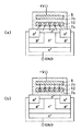
この後、フローティングゲート12への電荷注入を行う。この電荷注入の該略図を図7に示し、この図に基づいて電荷注入について説明する。
【0071】
電荷の注入は、フローティングゲート12と半導体(表面チャネル層5やソース領域4a、4b)間もしくはフローティングゲート12とゲート電極8の間に電荷の移動が発生するだけの電位をゲート電極8に印加することによって行う。これは、フローティングゲート12と半導体との間と、フローティングゲート12とゲート電極8との間のいずれが電流を流し易いかによって選択している。つまり、シリコン酸化膜7a、7bの膜質(膜厚分布や欠陥等)によって電流の流れ易さが決定されるため、電荷注入を行い易いようにシリコン酸化膜7a、7bの膜質を予め設定することも可能である。
【0072】
そして、フローティングゲート12と半導体との間の方が、フローティングゲート12とゲート電極8との間と比べて電流が流れやすい場合、図7(a)に示すように、ソース電極10、ドレイン電極11をアース状態としてゲート電極8に正の電圧を印加する。これにより、フローティングゲート12に負電荷として電子が注入される。また、フローティングゲート12とゲート電極8との間の方が、フローティングゲート12と半導体との間と比べて電流が流れやすい場合、図7(b)に示すように、ソース電極10、ドレイン電極11をアース状態としてゲート電極12に負の電圧を印加する。これにより、フローティングゲート12に負電荷として電子が注入される。
【0073】
このようして、図1に示すMOSFETが完成する。
【0074】
(第2実施形態)
図8に、本実施形態におけるMOSFETの断面構成を示す。なお、本実施形態では、第1実施形態のMOSFETのゲート構造を変更したものであるため、その変更部分についてのみ説明する。
【0075】
図8に示すように、本実施形態のMOSFETは、表面チャネル層5の上に、第1の絶縁膜としてのシリコン酸化膜7aを介して、シリコン窒化膜13が形成されている。そして、このシリコン窒化膜13の上にゲート電極8が形成されている。このように、ゲート電極8と表面チャネル層5との間に、シリコン酸化膜7aとシリコン窒化膜13からなる複合膜が配置されるようにしている。
【0076】
このような構成においては、シリコン窒化膜13とシリコン酸化膜7aとの界面において電荷をトラップすることができる。このため、この界面にトラップされた電荷が、第1実施形態のフローティングゲート12と同様の役割を果たし、ゲート電極8の電圧をオフセットすることができる。これにより、第1実施形態と同様の効果が得られる。
【0077】
なお、本実施形態におけるMOSFETは、図16に示す従来のMOSFETに対して、シリコン窒化膜13を形成する工程を増加させるのみであるため、わずかな工程上の負荷で電荷保持機構を実現することができる。
【0078】
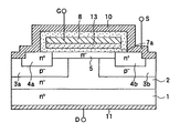
(第3実施形態)
図9に、本実施形態におけるMOSFETの断面構成を示す。本実施形態は、第1実施形態に対して、フローティングゲートに電荷を注入するに当たって、電荷注入が行われる領域を規定したものである。
【0079】
図9に示すように、本実施形態のMOSFETは、MOS作動領域の他に電荷注入を行う書き込み領域を形成している。なお、書き込み領域は、MOS作動領域とは他断面に設けられており、例えば、複数のMOSFETを敷き詰めてMOS作動領域を形成したとすると、その敷き詰められた領域から離れた位置に別途設けられている。
【0080】
書き込み領域は、いわゆるEPROMと同じ構造となっており、フローティングゲート12a及びゲート電極(コントロールゲート)8aの2層構造の両側に、ソース領域4c及びドレイン領域14が備えられ、このソース領域4cとドレイン領域14との間にチャネル領域となる表面チャネル層5cが備えられた構成となっている。なお、ソース領域4cはソース領域4bが延設されたものであり、ソース電極10に接続されている。このように、ソース領域4cとソース領域4bを兼用化することにより、装置の小型化を図っている。また、ドレイン領域14は、ドレイン電極15が接続されている。
【0081】
そして、MOS作動領域と書き込み領域におけるゲート電極8、8aがつながった構成となっていると共に、MOS作動領域と書き込み領域におけるフローティングゲート12、12aがつながった構成となっている(図中の点線部参照)。
【0082】
このような構成においては、図10に示すように書き込み領域にて電荷注入を行う。すなわち、ソース電極10及びドレイン電極11をアース状態にすると共に、ゲート電極8aに正電位V1、ドレイン電極に正電位V2をそれぞれ印加する。これにより、ホットキャリアを発生させ、フローティングゲート12aにホットエレクトロンを注入することができる。
【0083】
これにより、フローティングゲート12aに負電荷が注入されると、フローティングゲート12がフローティングゲート12aと接続されているため、フローティングゲート12の電位はゲート電極8の電位が零であっても負となる。これにより、MOS動作領域を第1実施形態と同様に動作させることができ、第1実施形態と同様の効果を得ることができる。
【0084】
そして、ホットキャリアを用いることで、書き込みを高速で行うことができる。また、MOS動作領域以外の領域で書き込みが行われるため、書き込み時にフローティングゲート12aの下のシリコン酸化膜7aがダメージを受けたとしても、MOS動作領域とは関係ない部分であるため、MOS動作に影響を与えることはない。なお、MOS動作時には、ドレイン電極15はオープン状態とするため、ドレイン領域14の電界による影響は無視して良い。
【0085】
なお、本実施形態におけるMOSFETの製造は、第1実施形態における図6(a)の工程のフォトリソグラフィ工程のマスクを変更すればよいだけであるため、説明を省略する。
【0086】
(第4実施形態)
図11に、本実施形態におけるMOSFETの断面構成を示す。本実施形態は、第1実施形態に対して、フローティングゲートに電荷を注入するに当たって、電荷注入が行われる領域を規定したものである。
【0087】
図11に示すように、本実施形態のMOSFETは、MOS作動領域の他に電荷注入を行う書き込み領域を形成している。なお、書き込み領域は、MOS作動領域とは他断面に設けられており、例えば、複数のMOSFETを敷き詰めてMOS作動領域を形成したとすると、その敷き詰められた領域から離れた位置に別途設けられている。
【0088】
書き込み領域は、フローティングゲート12a及びゲート電極(コントロールゲート)8aの2層構造で構成されており、ソース領域4bから延設されたソース領域4cの上に2層構造が形成された構成となっている。
【0089】
また、MOS作動領域と書き込み領域におけるフローティングゲート12、12aがつながった構成となっている(図中の点線部参照)。ただし、MOS作動領域と書き込み領域におけるゲート電極8、8aはつながった構成とされていない。
【0090】
このような構成においては、図12に示すように書き込み領域にて電荷注入を行う。すなわち、ゲート電極8とソース電極10及びドレイン電極11をアース状態にするとともに、ゲート電極8aに負電位−Vを印加する。
【0091】
通常、書き込み領域のゲート電極8aとフローティングゲート12aとの間の容量は、MOS動作領域のゲート電極8とフローティングゲート12との間の容量や、フローティングゲート12と半導体(本実施形態では表面チャネル層5やソース領域4a、4b)との間の容量と比べて非常に小さいため、フローティングゲート12の電位は書き込み領域のゲート電極8aの電位にほとんど影響されず、ゲート電極8と半導体の電位、つまりアース状態となる(ただし、書き込みされた電荷分だけ電位は変動する)。このため、書き込み領域のゲート電極8aとフローティングゲート12aとの間の電界が最大となり、書き込み領域のみ電荷注入が行われるようにできるとともに、FN電流により大量に書き込みが行われるようにできる。
【0092】
このように、上記構成とすることにより、大量に書き込みが行われるようにすることができると共に、第3実施形態と同様に、MOS動作領域以外の領域で書き込みを行えるため、書き込み時にフローティングゲート12aの上のシリコン酸化膜7bがダメージを受けたとしても、MOS動作に影響を与えることはない。また、FN電流を用いているため、書き込み領域や各領域とのコンタクトとしての書き込み端子を簡略化することができ、装置の小型化を図ることができる。
【0093】
なお、本実施形態におけるMOSFETの製造は、第1実施形態における図6(a)の工程のフォトリソグラフィ工程のマスクとして、2nd−polySiのエッチング時にゲート電極8とゲート電極8aが分割されるマスクを用い、その他については第3実施形態と同様にすればよいだけであるため、説明を省略する。
【0094】
また、本実施形態では、書き込み領域におけるフローティングゲート12の下部をソース領域4c、つまりn+型層で構成しているが、表面チャネル層5を延設する等によってn-型層で構成してもよく、ベース領域3bを延設する等によりp型層で構成したりしてもよい。
【0095】
(第5実施形態)
図13に、本実施形態におけるMOSFETの断面構成を示す。本実施形態は、第1実施形態に対して、フローティングゲートに電荷を注入するに当たって、電荷注入が行われる領域を規定したものである。
【0096】
図13に示すように、本実施形態のMOSFETは、ゲート電極8及びフローティングゲート12を表面チャネル層5から離れた領域まで延設し、この延設された部分に電荷注入が行われるように、この領域におけるフローティングゲート12の下部にシリコン酸化膜7aより薄いトンネル膜16を設けた構成としている。
【0097】
このように、書き込み窓としてシリコン酸化膜7aを部分的に薄膜化したトンネル膜16を設けることにより、このトンネル膜16から電荷が注入され易くすることができ、電荷が注入される領域を規定することができる。また、このように書き込みを行う場所を規定することにより、書き込み量の制御が容易となり、また大きな書き込み量を得ることができる。また、このような構成においては、別途書き込み端子を設ける必要がないため、装置を簡略化でき、小型化を図ることができる。
【0098】
なお、本実施形態におけるMOSFETは、第1実施形態における図6(a)においてシリコン酸化膜7aを形成したのち、シリコン酸化膜7aのうちのトンネル膜形成領域を一旦エッチング除去し、再度熱酸化することでトンネル膜16を形成すれば、その後は第1実施形態と同様の工程を施すことにより製造される。
【0099】
また、本実施形態では、シリコン酸化膜7aを薄膜化したが、電荷の注入方法によってはシリコン酸化膜7bを薄膜化してもよい。
【0100】
(第6実施形態)
図14に、本実施形態におけるMOSFETの断面構成を示す。本実施形態は、第1実施形態に対して、フローティングゲートに電荷を注入するに当たって、電荷注入が行われる領域を規定したものである。
【0101】
図14に示すように、本実施形態のMOSFETは、MOS作動領域の他に電荷注入を行う書き込み領域を形成している。なお、書き込み領域は、MOS作動領域とは他断面に設けられており、例えば、複数のMOSFETを敷き詰めてMOS作動領域を形成したとすると、その敷き詰められた領域から離れた位置に別途設けられている。
【0102】
書き込み領域は、フローティングゲート12a及びゲート電極(コントロールゲート)8aの2層構造で構成されており、ベース領域3a、3bと共に形成したp-型層3c及びこのp-型層3cの表層部に形成された書き込み用のドレインとしてのp+型層17の上部に2層構造が形成された構成となっている。なお、p+型層17にはドレイン電極18が接続されている。
【0103】
また、MOS作動領域と書き込み領域におけるフローティングゲート12、12aがつながった構成となっており、MOS作動領域と書き込み領域におけるゲート電極8、8aはつながった構成となっている(図中の点線部参照)。
【0104】
このような構成においては、ゲート電極8とソース電極10及びドレイン電極11をアース状態にするとともに、ドレイン電極18に負の電位を印加する。
【0105】
これにより、p+型層17側からフローティングゲート12aに電荷を注入することができる。このように、本実施形態の構成によっても第4実施形態と同様の効果を得ることができる。
【0106】
本実施形態におけるMOSFETは、p-型層3cをベース領域3a、3bを形成する際に同時に形成し、本図では示していないがベース領域3a、3bをソース電極10とコンタクトを取るためにベース領域3a、3bの表層部に形成するp+型のコンタクト層を形成する際にp+型層17を同時に形成すれば、第1実施形態に対して製造工程の増加なく製造される。なお、書き込み領域における2層ゲート構造は、第4実施形態と同様に、図6(a)に示す工程のフォトリソグラフィ工程におけるマスクを変更すれば、MOS動作領域と同時に形成される
(第7実施形態)
図15に本実施形態におけるMOSFETの断面構成を示す。本実施形態は、ラテラル型のMOSトランジスタに本発明の一実施形態を適用したものである。
【0107】
図15に示すように、n-型の半導体基板51の表層部にp-型層53が形成されており、このp型層53の表層部にn+型のソース領域54a、ドレイン領域54bが離間して形成され、さらにソース領域54aとドレイン領域54bとの間をつなぐように表面チャネル層55が形成されている。
【0108】
そして、表面チャネル層55の上部に第1の絶縁膜としてのシリコン酸化膜57aを介してフローティングゲート60が形成され、さらにフローティングゲート60の上に第2の絶縁膜としてのシリコン酸化膜57bを介してゲート電極58が形成されている。
【0109】
そして、ゲート電極58及びフローティングゲート60を含む基板表面全面に層間絶縁膜59が形成されており、層間絶縁膜59に形成された各コンタクトホールを通じて、ソース領域54a、ドレイン領域54b、ゲート電極58、及びp-型層53が各電極に接続されている。
【0110】
このように構成されたMOSトランジスタにおいても、第1実施形態と同様の方法によってフローティングゲート60に電荷を注入することで、フローティングゲート12を介して表面チャネル層5の表面の電界を変化させるようにし、オン抵抗の低減を図ることができ、電流能力を向上できると共に高速動作を可能にすることができる。
【0111】
(他の実施形態)
上記実施形態では、表面チャネル層5が従来よりも高濃度となるようにした場合について説明したが、従来よりも厚い層で形成される場合についても、MOSFETは上記実施形態と同様の動作を行い、同様にオン抵抗の低減を図ることができる。
【0112】
また、第7実施形態では、ラテラル型のMOSトランジスタにおいて、第1実施形態と同様の構造を採用した例を示したが第2〜第6実施形態と同様の構成を採用することも可能である。
【図面の簡単な説明】
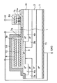
【図1】本発明の第1実施形態における縦型パワーMOSFETの断面図である。
【図2】フローティングゲート12に電荷を注入する前後におけるゲート電位とフローティングゲート電位との関係を示す図である。
【図3】ゲート電位及びフローティングゲート電位とドレイン電流の関係を示した図である。
【図4】図1に示す縦型パワーMOSFETの製造工程を示す図である。
【図5】図4に続く縦型パワーMOSFETの製造工程を示す図である。
【図6】図5に続く縦型パワーMOSFETの製造工程を示す図である。
【図7】第1実施形態におけるMOSFETの電荷注入方法を示した図である。
【図8】本発明の第2実施形態におけるMOSFETの断面図である。
【図9】本発明の第3実施形態におけるMOSFETの断面図である。
【図10】第3実施形態におけるMOSFETの電荷注入方法を示した図である。
【図11】本発明の第4実施形態におけるMOSFETの断面図である。
【図12】第4実施形態におけるMOSFETの電荷注入方法を示した図である。
【図13】本発明の第5実施形態におけるMOSFETの断面図である。
【図14】本発明の第6実施形態におけるMOSFETの断面図である。
【図15】本発明の第7実施形態におけるMOSFETの断面図である。
【図16】従来におけるMOSFETの断面図である。
【図17】表面チャネル層5を有するMOSFETのゲート電位とドレイン電流との関係を示した図である。
【符号の説明】
1…n+ 型基板、2…n- 型エピタキシャル層、
3a、3b…p- 型ベース領域、4a、4b…n+ 型ソース領域、
5…表面チャネル層(n- 型SiC層)、7…ゲート絶縁膜、8…ゲート電極、
9…絶縁膜、10…ソース電極、 11…ドレイン電極層、
12…フローティングゲート。[0001]
BACKGROUND OF THE INVENTION
The present invention relates to a silicon carbide semiconductor device and a method of manufacturing the same, and more particularly to an insulated gate field effect transistor, particularly a high power power MOSFET.
[0002]
[Prior art]
Conventionally, as a planar type MOSFET operating in the accumulation mode, one disclosed in Japanese Patent Application Laid-Open No. 11-308510 is known.
[0003]
A cross-sectional view of this planar MOSFET is shown in FIG. The structure of the planar MOSFET will be described with reference to this figure.
[0004]
n+Type silicon carbide semiconductor substrate (hereinafter n+The mold substrate 1) has an upper surface as a main surface 1a and a lower surface opposite to the main surface as a back surface 1b. This n+N having a lower dopant concentration than that of the
[0005]
n-The predetermined region in the surface layer portion of the
[0006]
N+
[0007]
The dopant concentration of the
[0008]
P-Mold
[0009]
The upper surface of the
[0010]
[Problems to be solved by the invention]
In the above conventional MOSFET, the on-resistance is reduced by operating in the accumulation mode. However, further reduction of on-resistance is desired.
[0011]
The present invention has been made in view of the above points, and an object thereof is to further reduce the on-resistance in an accumulation mode MOSFET.
[0012]
[Means for Solving the Problems]
In order to achieve the above object, the present inventors have studied an accumulation mode MOSFET. As the surface channel layer is concentrated and the threshold voltage is lowered, the on-current increases, that is, the on-resistance is reduced. It has been found that it can be reduced. FIG. 17 shows the relationship between the concentration of the surface channel layer and the on-current.
[0013]
As shown in this figure, the lower the threshold voltage, the larger the on-current. In particular, it was found that the on-current was significantly increased by using a negative depletion type MOS. .
[0014]
However, the depletion type MOSFET is normally on, and is not preferable from the viewpoint of fail-safe. Accordingly, the present inventors have further studied to obtain a MOSFET having an on-current equivalent to that of a depletion type MOSFET and having normally-on characteristics.
[0015]
Since the depletion type MOSFET has normally-on characteristics, switching can be performed by applying a negative voltage on the surface channel layer.
[0016]
That is, if a negative voltage is applied to the surface channel layer when no voltage is applied to the gate electrode (zero gate voltage), the enhancement type is positive (normally off characteristics). MOSFET.
[0017]
Therefore, in order to achieve the above object, the invention according to
[0018]
In this way, by providing the charge holding mechanism, the charge holding mechanism can be a negative potential even when the gate potential is used at zero or more, so that the on-resistance equivalent to the depletion type is obtained while maintaining the normally-off characteristic. It can be set as the silicon carbide semiconductor device which has.
[0021]
Also,Claim1 or 2In the invention described in (1), the semiconductor substrate has a MOS operation region in which a channel region is formed to perform a MOS operation, and a write region provided at a position different from the MOS operation region. The semiconductor device is characterized in that it extends from the MOS operation region to the writing region, and charges are injected into the writing region.
[0022]
Thus, by limiting the area rather than performing writing using the entire MOSFET, the amount of writing can be easily controlled and a large amount of writing can be obtained. In addition, by providing a write terminal, even if the gate insulating film is damaged in the charge injection portion at the time of writing, the damaged region is located at a position different from the MOS operation region, so that the normal MOS is not affected by the damaged region. Operation is possible.
In the writing region, a writing gate that is not electrically connected to the gate electrode in the MOS operation region may be formed on the floating gate, and a writing terminal may be connected to the gate.
Further, in the first or second aspect of the invention, the surface channel layer includes the source electrode and the drain electrode even under a condition in which no voltage is applied to the gate electrode in a state where the charge is not held in a mechanism capable of holding the charge. It is characterized in that electrical conduction between the two is possible.
Thus, if there is no offset of the gate voltage due to the charge holding mechanism, a particularly high current capability can be obtained in the case of a depletion type MOSFET, which is preferable.
[0023]
For example, as described in
Also,For example, claims4As shown in FIG. 2, in the writing region, a gate electrode extends from the MOS operation region to the writing region, and on the surface portion of the semiconductor substrate, both sides of the gate electrode and the floating gate in the writing region are provided.SeoSource and drain for writing,bookWhat is necessary is just to make it the structure which connected the terminal for writing to each of the drain for penetration.
[0024]
In such a configuration, charge injection can be performed using hot carriers. Thus, writing can be performed at high speed by using hot carrier injection.
[0026]
Claims5As shown in FIG. 2, the write region is provided with a gate electrode extending from the MOS operation region to the write region, and is not electrically connected to a base region or a well region disposed below the floating gate. A two-conductivity type writing drain may be provided, and a writing terminal connected to the writing drain may be provided.
[0027]
In such a configuration, charge injection can be performed using the FN current. In this manner, by using the FN current, the writing region and the writing terminal can be simplified and the size can be reduced.
[0030]
Claim6In the invention described in (1), the first gate insulating film or the second gate insulating film is partially thinned in the writing region.
[0031]
Thus, by partially thinning the first and second insulating films, a writing region can be set without providing a writing terminal. By limiting the area rather than performing writing using the entire MOSFET, the amount of writing can be easily controlled and a large amount of writing can be obtained. Further, since there is no writing terminal, the size can be reduced.
[0034]
In addition, the code | symbol in the bracket | parenthesis of each said means shows the correspondence with the specific means as described in embodiment mentioned later.
[0035]
DETAILED DESCRIPTION OF THE INVENTION
DESCRIPTION OF THE PREFERRED EMBODIMENTS Embodiments shown in the drawings will be described below.
[0036]
FIG. 1 shows a cross-sectional configuration of the MOSFET in the present embodiment. Hereinafter, the configuration of the MOSFET of this embodiment will be described with reference to FIG. However, among the MOSFETs of the present embodiment, the same or equivalent configurations as those of the conventional MOSFET shown in FIG. 16 are denoted by the same reference numerals as those in FIG. 16, and only different portions will be described.
[0037]
As shown in FIG. 1, in the MOSFET according to the present embodiment, a floating
[0038]
In the MOSFET configured as described above, by providing the floating
[0039]
That is, since the floating
[0040]
The total thickness of the
[0041]
Electrons are injected into the floating
[0042]
The offset of this electric field is set as follows.
[0043]
If the potential on the
[0044]
[Expression 1]
Vfg = (C2 · Vg + Q) / (C1 + C2)
Where Vfg is the floating gate potential, Vg is the gate potential, C1 is the capacitance between the floating
[0045]
Accordingly, by arbitrarily setting the charge Q in the floating
[0046]
Therefore, as described above, by injecting electrons as a negative charge into the floating
[0047]
FIG. 2 shows the relationship between the potential of the gate electrode 8 (hereinafter simply referred to as the gate potential) and the floating gate potential before and after electrons are injected into the floating
[0048]
This figure shows a case where the film thicknesses of the
[0049]
As shown in this figure, when electrons are injected into the floating
[0050]
FIG. 3 shows the relationship between the gate potential, the floating gate potential, and the drain current when the floating
[0051]
As shown in this figure, the
[0052]
Next, the operation (operation) of the MOSFET in this embodiment will be described.
[0053]
This MOSFET operates in a normally-off accumulation mode, and when no voltage is applied to the
[0054]
Subsequently, the potential of the floating
[0055]
At this time, electrons are n+From the
[0056]
As described above, a MOSFET operating as a depletion type without the floating
[0057]
As a result, as shown in FIG. 17, when the floating
[0058]
Next, the manufacturing process of the MOSFET in this embodiment will be described with reference to FIGS. Since the semiconductor region is the same as that of the conventional publication (Japanese Patent Laid-Open No. 11-308510), only different parts will be described.
[0059]
[Step shown in FIG. 4 (a)]
First, 4H or 6H SiC substrate, that is, n+
[0060]
[Step shown in FIG. 4B]
n-An
[0061]
[Step shown in FIG. 4 (c)]
After removing the
[0062]
[Step shown in FIG. 5A]
An
[0063]
[Step shown in FIG. 5B]
Then, after removing the
[0064]
[Step shown in FIG. 5 (c)]
After removing the
[0065]
Next, in order to form the floating
[0066]
Subsequently, after the 1st-
[0067]
[Step shown in FIG. 6A]
Then, 2nd-polySi21,
[0068]
Subsequently, the surfaces of the
[0069]
[Fig. 6 (bProcess shown in
Then, after forming contact holes in the
[0070]
Thereafter, charge is injected into the floating
[0071]
In charge injection, a potential sufficient to cause charge transfer between the floating
[0072]
When current flows more easily between the floating
[0073]
In this way, the MOSFET shown in FIG. 1 is completed.
[0074]
(Second Embodiment)
FIG. 8 shows a cross-sectional configuration of the MOSFET in this embodiment. In this embodiment, since the gate structure of the MOSFET of the first embodiment is changed, only the changed portion will be described.
[0075]
As shown in FIG. 8, in the MOSFET of this embodiment, a
[0076]
In such a configuration, charges can be trapped at the interface between the
[0077]
Note that the MOSFET in this embodiment only increases the number of steps of forming the
[0078]
(Third embodiment)
FIG. 9 shows a cross-sectional configuration of the MOSFET in this embodiment. This embodiment defines a region where charge injection is performed when injecting charges into the floating gate, as compared to the first embodiment.
[0079]
As shown in FIG. 9, the MOSFET of the present embodiment forms a write region for injecting charges in addition to the MOS operating region. The writing area is provided in a cross section other than the MOS operating area. For example, if the MOS operating area is formed by laying a plurality of MOSFETs, the writing area is separately provided at a position away from the laid area. Yes.
[0080]
The writing region has the same structure as a so-called EPROM, and a
[0081]
In addition, the
[0082]
In such a configuration, charge injection is performed in the write region as shown in FIG. That is, the
[0083]
Thus, when negative charges are injected into the floating
[0084]
By using hot carriers, writing can be performed at high speed. In addition, since writing is performed in a region other than the MOS operation region, even if the
[0085]
Note that the manufacture of the MOSFET in this embodiment is omitted because it is only necessary to change the mask of the photolithography step in the step of FIG. 6A in the first embodiment.
[0086]
(Fourth embodiment)
FIG. 11 shows a cross-sectional configuration of the MOSFET in the present embodiment. This embodiment defines a region where charge injection is performed when injecting charges into the floating gate, as compared to the first embodiment.
[0087]
As shown in FIG. 11, the MOSFET according to the present embodiment forms a write area for charge injection in addition to the MOS operating area. The writing area is provided in a cross section other than the MOS operating area. For example, if the MOS operating area is formed by laying a plurality of MOSFETs, the writing area is separately provided at a position away from the laid area. Yes.
[0088]
The writing region has a two-layer structure of a floating
[0089]
Further, the floating
[0090]
In such a configuration, charge injection is performed in the write region as shown in FIG. That is, the
[0091]
Usually, the capacitance between the
[0092]
As described above, with the above configuration, a large amount of data can be written, and, similarly to the third embodiment, data can be written in an area other than the MOS operation area. Even if the
[0093]
In the manufacture of the MOSFET in the present embodiment, a mask in which the
[0094]
In the present embodiment, the lower portion of the floating
[0095]
(Fifth embodiment)
FIG. 13 shows a cross-sectional configuration of the MOSFET in the present embodiment. This embodiment defines a region where charge injection is performed when injecting charges into the floating gate, as compared to the first embodiment.
[0096]
As shown in FIG. 13, in the MOSFET of this embodiment, the
[0097]
As described above, by providing the
[0098]
In the MOSFET according to the present embodiment, after forming the
[0099]
In this embodiment, the
[0100]
(Sixth embodiment)
FIG. 14 shows a cross-sectional configuration of the MOSFET in the present embodiment. This embodiment defines a region where charge injection is performed when injecting charges into the floating gate, as compared to the first embodiment.
[0101]
As shown in FIG. 14, the MOSFET of the present embodiment forms a write region for injecting charges in addition to the MOS operating region. The writing area is provided in a cross section other than the MOS operating area. For example, if the MOS operating area is formed by laying a plurality of MOSFETs, the writing area is separately provided at a position away from the laid area. Yes.
[0102]
The writing region has a two-layer structure of a floating
[0103]
Also, the floating
[0104]
In such a configuration, the
[0105]
As a result, p+Charge can be injected into the floating
[0106]
The MOSFET in this embodiment is p-The
(Seventh embodiment)
FIG. 15 shows a cross-sectional configuration of the MOSFET in this embodiment. In the present embodiment, one embodiment of the present invention is applied to a lateral type MOS transistor.
[0107]
As shown in FIG.-P on the surface layer of the semiconductor substrate 51-
[0108]
A floating
[0109]
An interlayer insulating film 59 is formed on the entire surface of the substrate including the
[0110]
Also in the MOS transistor configured as described above, the electric field on the surface of the
[0111]
(Other embodiments)
In the above embodiment, the case where the
[0112]
In the seventh embodiment, an example in which a lateral MOS transistor adopts the same structure as that of the first embodiment is shown. However, the same structure as that of the second to sixth embodiments can also be adopted. .
[Brief description of the drawings]
FIG. 1 is a cross-sectional view of a vertical power MOSFET according to a first embodiment of the present invention.
FIG. 2 is a diagram showing the relationship between the gate potential and the floating gate potential before and after the charge is injected into the floating
FIG. 3 is a diagram showing a relationship between a gate potential, a floating gate potential, and a drain current.
4 is a diagram showing a manufacturing process of the vertical power MOSFET shown in FIG. 1; FIG.
5 is a diagram showing the manufacturing process of the vertical power MOSFET subsequent to FIG. 4. FIG.
6 is a diagram showing the manufacturing process of the vertical power MOSFET subsequent to FIG. 5. FIG.
FIG. 7 is a diagram showing a method for injecting a MOSFET charge in the first embodiment.
FIG. 8 is a cross-sectional view of a MOSFET according to a second embodiment of the present invention.
FIG. 9 is a cross-sectional view of a MOSFET in a third embodiment of the present invention.
FIG. 10 is a diagram illustrating a method for injecting a MOSFET charge according to a third embodiment.
FIG. 11 is a cross-sectional view of a MOSFET in a fourth embodiment of the present invention.
FIG. 12 is a diagram showing a method for injecting a MOSFET charge according to the fourth embodiment.
FIG. 13 is a cross-sectional view of a MOSFET in a fifth embodiment of the present invention.
FIG. 14 is a cross-sectional view of a MOSFET according to a sixth embodiment of the present invention.
FIG. 15 is a cross-sectional view of a MOSFET in a seventh embodiment of the invention.
FIG. 16 is a cross-sectional view of a conventional MOSFET.
17 is a diagram showing the relationship between the gate potential and drain current of a MOSFET having a
[Explanation of symbols]
1 ... n+Mold substrate, 2 ... n-Type epitaxial layer,
3a, 3b ... p-Mold base region, 4a, 4b ... n+Type source area,
5 ... surface channel layer (n-Type SiC layer), 7 ... gate insulating film, 8 ... gate electrode,
9 ... Insulating film, 10 ... Source electrode, 11 ... Drain electrode layer,
12 ... Floating gate.
Claims (6)
前記半導体基板の主表面上に形成され、前記半導体基板よりも高抵抗な炭化珪素よりなる第1導電型の半導体層(2)と、
前記半導体層の表層部の所定領域に形成され、所定深さを有する第2導電型のベース領域(3a、3b)と、
前記ベース領域の表層部の所定領域に形成され、該ベース領域の深さよりも浅い第1導電型のソース領域(4a、4b)と、
前記ベース領域の表面部及び前記半導体層の表面部において、前記ソース領域と前記半導体層とを繋ぐように形成され、チャネル領域を形成する炭化珪素よりなる第1導電型の表面チャネル層(5)と、
前記表面チャネル層の表面に形成されたゲート絶縁膜(7a、7b)と、
前記ゲート絶縁膜の上に形成されたゲート電極(8)と、
前記ベース領域及び前記ソース領域に接触するように形成されたソース電極(10)と、
前記半導体基板の裏面に形成されたドレイン電極(11)とを備え、
前記ゲート絶縁膜は、第1のゲート絶縁膜(7a、57a)と第2のゲート絶縁膜(7b、57b)とを有して構成されており、該第1、第2のゲート絶縁膜の間には導電性のフローティングゲート(12、60)が配置され、該フローティングゲートに前記電荷を保持することにより、前記ゲート電極と前記表面チャネル層との間に電荷が保持できる機構が構成され、
前記半導体基板は、前記チャネル領域を形成してMOS動作を行うMOS動作領域と、該MOS動作領域とは異なる位置に設けられた書き込み領域とを有しており、
前記フローティングゲートは、前記MOS動作領域から前記書き込み領域まで延設され、該書き込み領域において、前記電荷が注入されるようになっており、
さらに、前記書き込み領域には、
前記フローティングゲート上に形成され、前記MOS動作領域における前記ゲート電極とは電気的に接続されていない、書き込み用ゲートと、
前記書き込み用ゲートに接続された書き込み用端子と、が備えられており、
前記表面チャネル層は、前記電荷が保持できる機構に電荷が保持されていない状態においては、前記ゲート電極に電圧が印加されない条件においても前記ソース電極と前記ドレイン電極の間の電気的導通が可能となっていることを特徴とする炭化珪素半導体装置。A first conductivity type semiconductor substrate (1) having a main surface and a back surface opposite to the main surface and made of silicon carbide;
A first conductivity type semiconductor layer (2) made of silicon carbide formed on the main surface of the semiconductor substrate and having a higher resistance than the semiconductor substrate;
A second conductivity type base region (3a, 3b) formed in a predetermined region of the surface layer portion of the semiconductor layer and having a predetermined depth;
A first conductivity type source region (4a, 4b) formed in a predetermined region of a surface layer portion of the base region and shallower than a depth of the base region;
A first conductivity type surface channel layer (5) made of silicon carbide, which is formed so as to connect the source region and the semiconductor layer at the surface portion of the base region and the surface portion of the semiconductor layer, and forms a channel region. When,
A gate insulating film (7a, 7b) formed on the surface of the surface channel layer;
A gate electrode (8) formed on the gate insulating film;
A source electrode (10) formed in contact with the base region and the source region;
A drain electrode (11) formed on the back surface of the semiconductor substrate;
The gate insulating film includes a first gate insulating film (7a, 57a) and a second gate insulating film (7b, 57b), and the first and second gate insulating films are formed. A conductive floating gate (12, 60) is disposed between them, and by holding the charge in the floating gate, a mechanism is formed that can hold the charge between the gate electrode and the surface channel layer ,
The semiconductor substrate has a MOS operation region that performs the MOS operation by forming the channel region, and a writing region provided at a position different from the MOS operation region,
The floating gate extends from the MOS operation region to the write region, and the charge is injected into the write region,
Furthermore, the writing area includes
A write gate formed on the floating gate and not electrically connected to the gate electrode in the MOS operation region;
A write terminal connected to the write gate, and
The surface channel layer is capable of electrical conduction between the source electrode and the drain electrode even when no voltage is applied to the gate electrode in a state where no charge is held in the mechanism capable of holding the charge. It is in silicon carbide semiconductor device, characterized in that are.
前記半導体基板の表層部の所定領域に形成され、所定深さを有する第2導電型のウェル領域(53)と、
前記ウェル領域の表層部の所定領域に形成され、該ウェル領域の深さよりも浅い第1導電型のソース領域(54a)とドレイン領域(54b)と、
前記ウェル領域の表面部において、前記ソース領域(54a)と前記ドレイン領域(54b)とを繋ぐように形成された、チャネル領域を形成する炭化珪素よりなる第1導電型の表面チャネル層(55)と、
前記表面チャネル層の表面に形成されたゲート絶縁膜(57a、57b)と、前記ゲート絶縁膜の上に形成されたゲート電極(58)と、
前記ソース領域(54a)に形成されたソース電極と、
前記ドレイン領域に形成されたドレイン電極と、
前記ウェル領域に形成された基板電極とを備え、
前記ゲート絶縁膜は、第1のゲート絶縁膜(7a、57a)と第2のゲート絶縁膜(7 b、57b)とを有して構成されており、該第1、第2のゲート絶縁膜の間には導電性のフローティングゲート(12、60)が配置され、該フローティングゲートに前記電荷を保持することにより、前記ゲート電極と前記表面チャネル層との間に電荷が保持できる機構が構成され、
前記半導体基板は、前記チャネル領域を形成してMOS動作を行うMOS動作領域と、該MOS動作領域とは異なる位置に設けられた書き込み領域とを有しており、
前記フローティングゲートは、前記MOS動作領域から前記書き込み領域まで延設され、該書き込み領域において、前記電荷が注入されるようになっており、
さらに、前記書き込み領域には、
前記フローティングゲート上に形成され、前記MOS動作領域における前記ゲート電極とは電気的に接続されていない、書き込み用ゲートと、
前記書き込み用ゲートに接続された書き込み用端子と、が備えられており、
前記表面チャネル層は、前記電荷が保持できる機構に電荷が保持されていない状態においては、前記ゲート電極に電圧が印加されない条件においても前記ソース電極と前記ドレイン電極の間の電気的導通が可能となっていることを特徴とする炭化珪素半導体装置。A semiconductor substrate (51) having a main surface and a back surface opposite to the main surface and made of silicon carbide;
A second conductivity type well region (53) formed in a predetermined region of the surface layer portion of the semiconductor substrate and having a predetermined depth;
A first conductivity type source region (54a) and a drain region (54b) formed in a predetermined region of a surface layer portion of the well region and shallower than a depth of the well region;
A surface channel layer (55) of the first conductivity type made of silicon carbide forming a channel region, which is formed so as to connect the source region (54a) and the drain region (54b) at the surface portion of the well region. When,
A gate insulating film (57a, 57b) formed on the surface of the surface channel layer; and a gate electrode (58) formed on the gate insulating film;
A source electrode formed in the source region (54a);
A drain electrode formed in the drain region;
A substrate electrode formed in the well region,
The gate insulating film includes a first gate insulating film (7a, 57a) and a second gate insulating film ( 7b, 57b). The first and second gate insulating films A conductive floating gate (12, 60) is disposed between the gate electrodes, and a mechanism for holding charges between the gate electrode and the surface channel layer by holding the charges in the floating gate is configured. ,
The semiconductor substrate has a MOS operation region that performs the MOS operation by forming the channel region, and a writing region provided at a position different from the MOS operation region,
The floating gate extends from the MOS operation region to the write region, and the charge is injected into the write region,
Furthermore, the writing area includes
A write gate formed on the floating gate and not electrically connected to the gate electrode in the MOS operation region;
A write terminal connected to the write gate, and
The surface channel layer is capable of electrical conduction between the source electrode and the drain electrode even when no voltage is applied to the gate electrode in a state where no charge is held in the mechanism capable of holding the charge. It is in silicon carbide semiconductor device, characterized in that are.
前記MOS動作領域から書き込み領域まで延設された前記ゲート電極と、
前記半導体基板の表面部に形成され、該書き込み領域における前記ゲート電極及び前記フローティングゲートの両側に配置されたソース及び書き込み用ドレインと、
前記書き込み用ドレインに接続された書き込み用端子と、が備えられていることを特徴とする請求項1ないし3のいずれか1つに記載の炭化珪素半導体装置。In the writing area,
The gate electrode extending from the MOS operating region to the writing region;
Wherein formed on the surface portion of the semiconductor substrate, and the gate electrode and the floating gate source over scan and write drain arranged on either side of the said writing area,
The silicon carbide semiconductor device according to any one of claims 1 to 3, characterized in that the write terminal connected before Symbol drain for writing, are provided.
Priority Applications (1)
| Application Number | Priority Date | Filing Date | Title |
|---|---|---|---|
| JP26753499A JP4277381B2 (en) | 1999-09-21 | 1999-09-21 | Silicon carbide semiconductor device and manufacturing method thereof |
Applications Claiming Priority (1)
| Application Number | Priority Date | Filing Date | Title |
|---|---|---|---|
| JP26753499A JP4277381B2 (en) | 1999-09-21 | 1999-09-21 | Silicon carbide semiconductor device and manufacturing method thereof |
Publications (3)
| Publication Number | Publication Date |
|---|---|
| JP2001094099A JP2001094099A (en) | 2001-04-06 |
| JP2001094099A5 JP2001094099A5 (en) | 2006-02-09 |
| JP4277381B2 true JP4277381B2 (en) | 2009-06-10 |
Family
ID=17446168
Family Applications (1)
| Application Number | Title | Priority Date | Filing Date |
|---|---|---|---|
| JP26753499A Expired - Fee Related JP4277381B2 (en) | 1999-09-21 | 1999-09-21 | Silicon carbide semiconductor device and manufacturing method thereof |
Country Status (1)
| Country | Link |
|---|---|
| JP (1) | JP4277381B2 (en) |
Families Citing this family (8)
| Publication number | Priority date | Publication date | Assignee | Title |
|---|---|---|---|---|
| KR20050056200A (en) * | 2002-08-13 | 2005-06-14 | 제네럴 세미컨덕터, 인코포레이티드 | A dmos device with a programmable threshold voltage |
| TWI313060B (en) | 2003-07-28 | 2009-08-01 | Japan Science & Tech Agency | Feild effect transisitor and fabricating method thereof |
| US8174809B2 (en) * | 2006-07-26 | 2012-05-08 | Koninklijke Philips Electronics N.V. | Arrangement and method for deactivating electrical elements when malfunctioning |
| US20120019284A1 (en) * | 2010-07-26 | 2012-01-26 | Infineon Technologies Austria Ag | Normally-Off Field Effect Transistor, a Manufacturing Method Therefor and a Method for Programming a Power Field Effect Transistor |
| JP6606847B2 (en) * | 2015-04-01 | 2019-11-20 | 富士電機株式会社 | Silicon carbide semiconductor device and processing method thereof |
| JP6711102B2 (en) * | 2016-04-19 | 2020-06-17 | 富士電機株式会社 | Insulated gate type semiconductor device and method of manufacturing insulated gate type semiconductor device |
| CN112864234B (en) * | 2019-11-27 | 2022-04-15 | 苏州东微半导体股份有限公司 | IGBT power device |
| CN112885900B (en) * | 2019-11-29 | 2022-04-15 | 苏州东微半导体股份有限公司 | IGBT device |
-
1999
- 1999-09-21 JP JP26753499A patent/JP4277381B2/en not_active Expired - Fee Related
Also Published As
| Publication number | Publication date |
|---|---|
| JP2001094099A (en) | 2001-04-06 |
Similar Documents
| Publication | Publication Date | Title |
|---|---|---|
| JP4192353B2 (en) | Silicon carbide semiconductor device and manufacturing method thereof | |
| US8035112B1 (en) | SIC power DMOSFET with self-aligned source contact | |
| JP3428459B2 (en) | Silicon carbide n-channel MOS semiconductor device and method of manufacturing the same | |
| JPH11266017A (en) | Silicon carbide semiconductor device and manufacture thereof | |
| JPWO2009050871A1 (en) | Semiconductor device and manufacturing method thereof | |
| WO2006054394A1 (en) | Silicon carbide mos field-effect transistor and process for producing the same | |
| JP3661664B2 (en) | Silicon carbide semiconductor device and manufacturing method thereof | |
| JP4806852B2 (en) | Silicon carbide semiconductor device and manufacturing method thereof | |
| JP4277381B2 (en) | Silicon carbide semiconductor device and manufacturing method thereof | |
| JPWO2019142529A1 (en) | Semiconductor devices and their manufacturing methods | |
| US6268626B1 (en) | DMOS field effect transistor with improved electrical characteristics and method for manufacturing the same | |
| JP5033305B2 (en) | Silicon carbide semiconductor device | |
| US7768035B2 (en) | Semiconductor device and method of manufacturing the same | |
| JP2005252157A (en) | Semiconductor device and manufacturing method therefor | |
| US5923051A (en) | Field controlled semiconductor device of SiC and a method for production thereof | |
| US8110870B2 (en) | Semiconductor device | |
| JP3496509B2 (en) | Method for manufacturing silicon carbide semiconductor device | |
| JP3690594B2 (en) | Nitride compound semiconductor field effect transistor | |
| JPH10125904A (en) | Silicon carbide semiconductor device | |
| US9048103B2 (en) | Method for producing semiconductor device | |
| JPH11354791A (en) | Silicon carbide semiconductor device and its manufacture | |
| JP2016025324A (en) | Semiconductor device and control method for the same | |
| JP2009170598A (en) | Semiconductor device and method for producing the same | |
| JPH10107269A (en) | Semiconductor device controllable by field effect and its manufacture | |
| JP3952814B2 (en) | Silicon carbide semiconductor device and manufacturing method thereof |
Legal Events
| Date | Code | Title | Description |
|---|---|---|---|
| A521 | Written amendment |
Free format text: JAPANESE INTERMEDIATE CODE: A523 Effective date: 20051220 |
|
| A621 | Written request for application examination |
Free format text: JAPANESE INTERMEDIATE CODE: A621 Effective date: 20051220 |
|
| A977 | Report on retrieval |
Free format text: JAPANESE INTERMEDIATE CODE: A971007 Effective date: 20081119 |
|
| A131 | Notification of reasons for refusal |
Free format text: JAPANESE INTERMEDIATE CODE: A131 Effective date: 20081125 |
|
| A521 | Written amendment |
Free format text: JAPANESE INTERMEDIATE CODE: A523 Effective date: 20090121 |
|
| TRDD | Decision of grant or rejection written | ||
| A01 | Written decision to grant a patent or to grant a registration (utility model) |
Free format text: JAPANESE INTERMEDIATE CODE: A01 Effective date: 20090217 |
|
| A01 | Written decision to grant a patent or to grant a registration (utility model) |
Free format text: JAPANESE INTERMEDIATE CODE: A01 |
|
| A61 | First payment of annual fees (during grant procedure) |
Free format text: JAPANESE INTERMEDIATE CODE: A61 Effective date: 20090302 |
|
| FPAY | Renewal fee payment (event date is renewal date of database) |
Free format text: PAYMENT UNTIL: 20120319 Year of fee payment: 3 |
|
| R150 | Certificate of patent or registration of utility model |
Free format text: JAPANESE INTERMEDIATE CODE: R150 |
|
| FPAY | Renewal fee payment (event date is renewal date of database) |
Free format text: PAYMENT UNTIL: 20120319 Year of fee payment: 3 |
|
| FPAY | Renewal fee payment (event date is renewal date of database) |
Free format text: PAYMENT UNTIL: 20130319 Year of fee payment: 4 |
|
| FPAY | Renewal fee payment (event date is renewal date of database) |
Free format text: PAYMENT UNTIL: 20140319 Year of fee payment: 5 |
|
| R250 | Receipt of annual fees |
Free format text: JAPANESE INTERMEDIATE CODE: R250 |
|
| R250 | Receipt of annual fees |
Free format text: JAPANESE INTERMEDIATE CODE: R250 |
|
| R250 | Receipt of annual fees |
Free format text: JAPANESE INTERMEDIATE CODE: R250 |
|
| R250 | Receipt of annual fees |
Free format text: JAPANESE INTERMEDIATE CODE: R250 |
|
| LAPS | Cancellation because of no payment of annual fees |