JP4275095B2 - Manufacturing method of semiconductor chip - Google Patents
Manufacturing method of semiconductor chip Download PDFInfo
- Publication number
- JP4275095B2 JP4275095B2 JP2005117221A JP2005117221A JP4275095B2 JP 4275095 B2 JP4275095 B2 JP 4275095B2 JP 2005117221 A JP2005117221 A JP 2005117221A JP 2005117221 A JP2005117221 A JP 2005117221A JP 4275095 B2 JP4275095 B2 JP 4275095B2
- Authority
- JP
- Japan
- Prior art keywords
- etching
- plasma
- semiconductor wafer
- semiconductor chip
- mask
- Prior art date
- Legal status (The legal status is an assumption and is not a legal conclusion. Google has not performed a legal analysis and makes no representation as to the accuracy of the status listed.)
- Active
Links
Images


Classifications
-
- H—ELECTRICITY
- H01—ELECTRIC ELEMENTS
- H01L—SEMICONDUCTOR DEVICES NOT COVERED BY CLASS H10
- H01L21/00—Processes or apparatus adapted for the manufacture or treatment of semiconductor or solid state devices or of parts thereof
- H01L21/67—Apparatus specially adapted for handling semiconductor or electric solid state devices during manufacture or treatment thereof; Apparatus specially adapted for handling wafers during manufacture or treatment of semiconductor or electric solid state devices or components ; Apparatus not specifically provided for elsewhere
- H01L21/683—Apparatus specially adapted for handling semiconductor or electric solid state devices during manufacture or treatment thereof; Apparatus specially adapted for handling wafers during manufacture or treatment of semiconductor or electric solid state devices or components ; Apparatus not specifically provided for elsewhere for supporting or gripping
- H01L21/6835—Apparatus specially adapted for handling semiconductor or electric solid state devices during manufacture or treatment thereof; Apparatus specially adapted for handling wafers during manufacture or treatment of semiconductor or electric solid state devices or components ; Apparatus not specifically provided for elsewhere for supporting or gripping using temporarily an auxiliary support
-
- H—ELECTRICITY
- H01—ELECTRIC ELEMENTS
- H01L—SEMICONDUCTOR DEVICES NOT COVERED BY CLASS H10
- H01L21/00—Processes or apparatus adapted for the manufacture or treatment of semiconductor or solid state devices or of parts thereof
- H01L21/02—Manufacture or treatment of semiconductor devices or of parts thereof
- H01L21/04—Manufacture or treatment of semiconductor devices or of parts thereof the devices having at least one potential-jump barrier or surface barrier, e.g. PN junction, depletion layer or carrier concentration layer
- H01L21/18—Manufacture or treatment of semiconductor devices or of parts thereof the devices having at least one potential-jump barrier or surface barrier, e.g. PN junction, depletion layer or carrier concentration layer the devices having semiconductor bodies comprising elements of Group IV of the Periodic System or AIIIBV compounds with or without impurities, e.g. doping materials
- H01L21/30—Treatment of semiconductor bodies using processes or apparatus not provided for in groups H01L21/20 - H01L21/26
- H01L21/302—Treatment of semiconductor bodies using processes or apparatus not provided for in groups H01L21/20 - H01L21/26 to change their surface-physical characteristics or shape, e.g. etching, polishing, cutting
- H01L21/306—Chemical or electrical treatment, e.g. electrolytic etching
- H01L21/3065—Plasma etching; Reactive-ion etching
-
- H—ELECTRICITY
- H01—ELECTRIC ELEMENTS
- H01L—SEMICONDUCTOR DEVICES NOT COVERED BY CLASS H10
- H01L21/00—Processes or apparatus adapted for the manufacture or treatment of semiconductor or solid state devices or of parts thereof
- H01L21/02—Manufacture or treatment of semiconductor devices or of parts thereof
- H01L21/04—Manufacture or treatment of semiconductor devices or of parts thereof the devices having at least one potential-jump barrier or surface barrier, e.g. PN junction, depletion layer or carrier concentration layer
- H01L21/18—Manufacture or treatment of semiconductor devices or of parts thereof the devices having at least one potential-jump barrier or surface barrier, e.g. PN junction, depletion layer or carrier concentration layer the devices having semiconductor bodies comprising elements of Group IV of the Periodic System or AIIIBV compounds with or without impurities, e.g. doping materials
- H01L21/30—Treatment of semiconductor bodies using processes or apparatus not provided for in groups H01L21/20 - H01L21/26
- H01L21/31—Treatment of semiconductor bodies using processes or apparatus not provided for in groups H01L21/20 - H01L21/26 to form insulating layers thereon, e.g. for masking or by using photolithographic techniques; After treatment of these layers; Selection of materials for these layers
- H01L21/3105—After-treatment
- H01L21/311—Etching the insulating layers by chemical or physical means
- H01L21/31105—Etching inorganic layers
- H01L21/31111—Etching inorganic layers by chemical means
- H01L21/31116—Etching inorganic layers by chemical means by dry-etching
-
- H—ELECTRICITY
- H01—ELECTRIC ELEMENTS
- H01L—SEMICONDUCTOR DEVICES NOT COVERED BY CLASS H10
- H01L21/00—Processes or apparatus adapted for the manufacture or treatment of semiconductor or solid state devices or of parts thereof
- H01L21/02—Manufacture or treatment of semiconductor devices or of parts thereof
- H01L21/04—Manufacture or treatment of semiconductor devices or of parts thereof the devices having at least one potential-jump barrier or surface barrier, e.g. PN junction, depletion layer or carrier concentration layer
- H01L21/18—Manufacture or treatment of semiconductor devices or of parts thereof the devices having at least one potential-jump barrier or surface barrier, e.g. PN junction, depletion layer or carrier concentration layer the devices having semiconductor bodies comprising elements of Group IV of the Periodic System or AIIIBV compounds with or without impurities, e.g. doping materials
- H01L21/30—Treatment of semiconductor bodies using processes or apparatus not provided for in groups H01L21/20 - H01L21/26
- H01L21/31—Treatment of semiconductor bodies using processes or apparatus not provided for in groups H01L21/20 - H01L21/26 to form insulating layers thereon, e.g. for masking or by using photolithographic techniques; After treatment of these layers; Selection of materials for these layers
- H01L21/3105—After-treatment
- H01L21/311—Etching the insulating layers by chemical or physical means
- H01L21/31127—Etching organic layers
- H01L21/31133—Etching organic layers by chemical means
- H01L21/31138—Etching organic layers by chemical means by dry-etching
-
- H—ELECTRICITY
- H01—ELECTRIC ELEMENTS
- H01L—SEMICONDUCTOR DEVICES NOT COVERED BY CLASS H10
- H01L21/00—Processes or apparatus adapted for the manufacture or treatment of semiconductor or solid state devices or of parts thereof
- H01L21/70—Manufacture or treatment of devices consisting of a plurality of solid state components formed in or on a common substrate or of parts thereof; Manufacture of integrated circuit devices or of parts thereof
- H01L21/77—Manufacture or treatment of devices consisting of a plurality of solid state components or integrated circuits formed in, or on, a common substrate
- H01L21/78—Manufacture or treatment of devices consisting of a plurality of solid state components or integrated circuits formed in, or on, a common substrate with subsequent division of the substrate into plural individual devices
-
- H—ELECTRICITY
- H01—ELECTRIC ELEMENTS
- H01J—ELECTRIC DISCHARGE TUBES OR DISCHARGE LAMPS
- H01J2237/00—Discharge tubes exposing object to beam, e.g. for analysis treatment, etching, imaging
- H01J2237/32—Processing objects by plasma generation
- H01J2237/33—Processing objects by plasma generation characterised by the type of processing
- H01J2237/334—Etching
-
- H—ELECTRICITY
- H01—ELECTRIC ELEMENTS
- H01L—SEMICONDUCTOR DEVICES NOT COVERED BY CLASS H10
- H01L2221/00—Processes or apparatus adapted for the manufacture or treatment of semiconductor or solid state devices or of parts thereof covered by H01L21/00
- H01L2221/67—Apparatus for handling semiconductor or electric solid state devices during manufacture or treatment thereof; Apparatus for handling wafers during manufacture or treatment of semiconductor or electric solid state devices or components; Apparatus not specifically provided for elsewhere
- H01L2221/683—Apparatus for handling semiconductor or electric solid state devices during manufacture or treatment thereof; Apparatus for handling wafers during manufacture or treatment of semiconductor or electric solid state devices or components; Apparatus not specifically provided for elsewhere for supporting or gripping
- H01L2221/68304—Apparatus for handling semiconductor or electric solid state devices during manufacture or treatment thereof; Apparatus for handling wafers during manufacture or treatment of semiconductor or electric solid state devices or components; Apparatus not specifically provided for elsewhere for supporting or gripping using temporarily an auxiliary support
- H01L2221/6834—Apparatus for handling semiconductor or electric solid state devices during manufacture or treatment thereof; Apparatus for handling wafers during manufacture or treatment of semiconductor or electric solid state devices or components; Apparatus not specifically provided for elsewhere for supporting or gripping using temporarily an auxiliary support used to protect an active side of a device or wafer
-
- H—ELECTRICITY
- H01—ELECTRIC ELEMENTS
- H01L—SEMICONDUCTOR DEVICES NOT COVERED BY CLASS H10
- H01L2221/00—Processes or apparatus adapted for the manufacture or treatment of semiconductor or solid state devices or of parts thereof covered by H01L21/00
- H01L2221/67—Apparatus for handling semiconductor or electric solid state devices during manufacture or treatment thereof; Apparatus for handling wafers during manufacture or treatment of semiconductor or electric solid state devices or components; Apparatus not specifically provided for elsewhere
- H01L2221/683—Apparatus for handling semiconductor or electric solid state devices during manufacture or treatment thereof; Apparatus for handling wafers during manufacture or treatment of semiconductor or electric solid state devices or components; Apparatus not specifically provided for elsewhere for supporting or gripping
- H01L2221/68304—Apparatus for handling semiconductor or electric solid state devices during manufacture or treatment thereof; Apparatus for handling wafers during manufacture or treatment of semiconductor or electric solid state devices or components; Apparatus not specifically provided for elsewhere for supporting or gripping using temporarily an auxiliary support
- H01L2221/68354—Apparatus for handling semiconductor or electric solid state devices during manufacture or treatment thereof; Apparatus for handling wafers during manufacture or treatment of semiconductor or electric solid state devices or components; Apparatus not specifically provided for elsewhere for supporting or gripping using temporarily an auxiliary support used to support diced chips prior to mounting
-
- H—ELECTRICITY
- H01—ELECTRIC ELEMENTS
- H01L—SEMICONDUCTOR DEVICES NOT COVERED BY CLASS H10
- H01L2924/00—Indexing scheme for arrangements or methods for connecting or disconnecting semiconductor or solid-state bodies as covered by H01L24/00
- H01L2924/30—Technical effects
- H01L2924/301—Electrical effects
- H01L2924/30105—Capacitance
Landscapes
- Engineering & Computer Science (AREA)
- Physics & Mathematics (AREA)
- Computer Hardware Design (AREA)
- Condensed Matter Physics & Semiconductors (AREA)
- General Physics & Mathematics (AREA)
- Manufacturing & Machinery (AREA)
- Microelectronics & Electronic Packaging (AREA)
- Power Engineering (AREA)
- Chemical & Material Sciences (AREA)
- Chemical Kinetics & Catalysis (AREA)
- General Chemical & Material Sciences (AREA)
- Plasma & Fusion (AREA)
- Inorganic Chemistry (AREA)
- Dicing (AREA)
- Drying Of Semiconductors (AREA)
Description
本発明は、分割領域により画定される複数の素子形成領域内に配置される半導体素子を、半導体ウェハの第1の面において形成し、当該半導体ウェハに対して上記分割領域において上記各々の素子形成領域を個別に分割して、個片化された上記半導体素子を含む半導体チップを製造する半導体チップの製造方法及び半導体チップに関する。 According to the present invention, a semiconductor element disposed in a plurality of element forming regions defined by divided regions is formed on a first surface of a semiconductor wafer, and each element is formed in the divided region with respect to the semiconductor wafer. The present invention relates to a semiconductor chip manufacturing method and a semiconductor chip for manufacturing a semiconductor chip including the semiconductor element divided into pieces by dividing the region individually.
従来、このような半導体チップの製造方法において、半導体ウェハを個々の半導体チップに分割する方法としては、様々なものが知られている。例えば、ダイサーのブレードと呼ばれる回転刃を用いて機械的に切断することで、半導体ウェハの分割を行う方法、すなわち機械的なダイシングが知られている。 Conventionally, in such a semiconductor chip manufacturing method, various methods are known for dividing a semiconductor wafer into individual semiconductor chips. For example, a method of dividing a semiconductor wafer by mechanically cutting using a rotary blade called a dicer blade, that is, mechanical dicing is known.
しかしながら、近年半導体ウェハは益々薄化され、外力に対する強度が弱い半導体ウェハに対して、このような機械的なダイシングを施すような場合にあっては、切断時に半導体ウェハにダメージを与える場合も多く、加工歩留まりの低下を避けることができないという問題がある。このようなダメージとしては、例えば、切断された鋭利な形状により、半導体チップの角部(エッジ)に欠けが生じるというチッピングの発生がある。 However, in recent years, semiconductor wafers have become increasingly thinner, and when such mechanical dicing is applied to semiconductor wafers that are weak against external forces, the semiconductor wafers are often damaged during cutting. However, there is a problem that a reduction in processing yield cannot be avoided. Such damage includes, for example, chipping in which a chipped portion has a chipped corner due to a sharp cut shape.
このような従来の機械的なダイシングに代わって、近年、プラズマエッチングを用いたプラズマダイシングが注目されつつある(例えば、特許文献1参照)。ここで、この従来のプラズマダイシングにより半導体ウェハを個々の半導体チップに分割する方法について、図27(A)〜(C)、及び図28(A)、(B)に示す模式説明図を用いて以下に説明する。 In recent years, plasma dicing using plasma etching has been attracting attention in place of such conventional mechanical dicing (see, for example, Patent Document 1). Here, a method for dividing a semiconductor wafer into individual semiconductor chips by the conventional plasma dicing will be described with reference to schematic explanatory views shown in FIGS. 27 (A) to (C) and FIGS. 28 (A) and 28 (B). This will be described below.
まず、図27(A)に示すように、半導体ウェハ501は、その回路形成面501aにおいて、分割領域R2により画定されるそれぞれの素子形成領域R1内に半導体素子502が形成された状態とされている。それぞれの半導体素子502は、半導体ウェハ501(Semiconductor)と、回路形成面501a上に直接的に形成されたシリコン酸化膜551(Oxide)と、このシリコン酸化膜551上に形成された金属膜(Metal)とで構成されるMOS(Metal−Oxide−Semiconductor)構造トランジスタ等のデバイス群を含んでいる。さらに、半導体素子502は、デバイス群を外部の電子装置と電気的に接続する為の接続端子552(ボンディングパッドとも呼ぶ)も備えている。また、それぞれの半導体素子502の表面には表面保護膜553が形成され、半導体素子502の表面が保護されている。接続端子552は表面保護膜553で覆われず外部に露呈している。なお、回路形成面501aにおける分割領域R2に相当する部分には、シリコン酸化膜551及び表面保護膜553は形成されていない。
First, as shown in FIG. 27A, the
次に、図27(B)に示すように、半導体ウェハ501の回路形成面501aが損傷を受けることがないように、回路形成面501aに保護シート504を、粘着剤を介して剥離可能に貼着し、その後、回路形成面501aとは反対側の面である被処理面501bに、分割領域R2に相当する部分が露出するようにマスク(マスクパターン)505を配置する。
Next, as shown in FIG. 27B, a
次に、このようにマスク505が形成された半導体ウェハ501に対してプラズマエッチングを行うことにより、被処理面501bにおいてマスク505に覆われていない露出表面に対してエッチングを施し、分割領域R2に相当する部分の除去を行う。これにより図27(C)に示すように、それぞれの素子形成領域R1が個別に分割されて、半導体素子502を含む半導体チップ510の個片が形成され、その結果、半導体ウェハ501は、分割領域R2に沿ってそれぞれの半導体素子502を含む半導体チップ510の個片に分割されることとなる。
Next, plasma etching is performed on the
その後、図28(A)に示すように、分割されたそれぞれの半導体チップ510の被処理面501bに残存しているマスク505を、例えばアッシング処理を施すことで除去する。さらにその後、図28(B)に示すように、半導体ウェハ501の被処理面501bに粘着シート(ダイシングシート)506を貼り付けるとともに、半導体ウェハ501の回路形成面501aを保護していた保護シート504を剥離する。これにより、それぞれの半導体チップ510が個片に分割された状態で粘着シート506上に配置された状態とされることとなる。
Thereafter, as shown in FIG. 28A, the
このような従来のプラズマダイシングを用いて、半導体ウェハ501の分割を行うことにより、上述の機械的なダイシングに比べて、製造された半導体チップ510に与えられるダメージを少なくさせることができる。
By dividing the
しかしながら、このような従来のプラズマダイシングにより個片に分割された半導体チップ510においても、図27(C)、及び図28(A)、(B)に示すように、当該分割により鋭利な角部554(エッジ)が形成されることとなる。このように半導体チップ510において鋭利な角部554が形成されるような場合にあっては、上記チッピングが生じることを避けることができないという問題がある。
However, also in the
特に、このような従来のプラズマダイシングにおいては、プラズマ中のイオンがエッチング底部に行くほど到達し難いという特性を有していることから、例えば図29に示すエッチングが施された分割領域R2の部分拡大模式図に示すように、分割された半導体チップ510の下方端部には、突出するような鋭利な角部554が形成されるような場合もある。このような場合にあっては、角部554の欠けがさらに生じやすく、半導体チップにおける抗折強度が低下するという問題がある。
In particular, such conventional plasma dicing has a characteristic that ions in the plasma are less likely to reach the bottom of the etching. Therefore, for example, a portion of the divided region R2 subjected to the etching shown in FIG. As shown in the enlarged schematic diagram, a
さらに、半導体チップ510においては、図29に示すように、回路形成面501aにおいてこのような鋭利な角部554が形成されるだけでなく、被処理面501bにおいても鋭利な角部555が形成されることとなり、半導体チップ510における抗折強度の低下がさらに顕著となるという問題がある。
Furthermore, in the
従って、本発明の目的は、上記問題を解決することにあって、半導体ウェハを分割することで、個片化された半導体チップを形成する半導体チップの製造方法において、それぞれの半導体チップを損傷させることなく、高い抗折強度を備えさせることができる半導体チップの製造方法及びこのような高い抗折強度を有する半導体チップを提供することにある。 Accordingly, an object of the present invention is to solve the above-described problems, and in a semiconductor chip manufacturing method in which semiconductor chips are formed by dividing a semiconductor wafer, each semiconductor chip is damaged. It is an object of the present invention to provide a method for manufacturing a semiconductor chip capable of providing a high bending strength and a semiconductor chip having such a high bending strength.
上記目的を達成するために、本発明は以下のように構成する。 In order to achieve the above object, the present invention is configured as follows.
本発明の第1態様によれば、分割領域により画定される複数の素子形成領域内に配置される半導体素子を、半導体ウェハの第1の面において形成し、当該半導体ウェハに対して上記分割領域において上記各々の素子形成領域を個別に分割して、個片化された上記半導体素子を含む半導体チップを製造する方法であって、
上記第1の面における上記分割領域に絶縁膜が配置され、当該第1の面とは反対側の面である第2の面に当該分割領域を画定するためのマスクを形成する工程と、
上記マスクが形成されたマスク付きの半導体ウェハに対して、上記第2の面よりプラズマエッチングを施すことにより、上記分割領域に相当する部分を除去してエッチング底部より上記絶縁膜を露呈させる絶縁膜露呈工程と、
当該絶縁膜露呈工程の後、プラズマ中のイオンにより当該露呈された絶縁膜上に電荷を帯電させた状態にて、上記プラズマエッチングを行うことで、上記各々の素子形成領域において、上記絶縁膜に接する上記第1の面側におけるそれぞれの角部の除去を行う角部除去工程と、
当該角部除去工程の後、当該露呈された絶縁膜を除去して、上記各々の素子形成領域を個々の上記半導体チップに分割する絶縁膜除去工程とを含み、
上記絶縁膜露呈工程、上記角部除去工程、又は上記絶縁膜除去工程の実施前あるいは実施後のいずれかのタイミングにおいて、上記マスクが配置された状態の上記半導体ウェハ若しくは上記個々の半導体チップに対して、等方性プラズマエッチングを実施することを特徴とする半導体チップの製造方法を提供する。
According to the first aspect of the present invention, the semiconductor elements disposed in the plurality of element formation regions defined by the divided regions are formed on the first surface of the semiconductor wafer, and the divided regions are formed on the semiconductor wafer. In which each of the element formation regions is individually divided to manufacture a semiconductor chip including the semiconductor element separated into pieces,
Forming an insulating film in the divided region on the first surface, and forming a mask for defining the divided region on a second surface that is a surface opposite to the first surface ;
An insulating film that exposes the insulating film from an etching bottom by removing a portion corresponding to the divided region by performing plasma etching on the semiconductor wafer with the mask on which the mask is formed from the second surface. An exposure process;
After the insulating film exposure step, the plasma etching is performed in a state where electric charges are charged on the exposed insulating film by ions in the plasma, so that the insulating film is formed in each element forming region. A corner removal step of removing each corner on the first surface side in contact;
After the corner portion removing step, the exposed insulating film is removed, and an insulating film removing step for dividing each element forming region into the individual semiconductor chips,
At any timing before or after the insulating film exposing step, the corner removing step, or the insulating film removing step, the semiconductor wafer or the individual semiconductor chips in a state where the mask is disposed. Thus, a method for manufacturing a semiconductor chip is provided, wherein isotropic plasma etching is performed.
本発明の第2態様によれば、上記等方性プラズマエッチングの実施により、上記半導体ウェハ又は上記それぞれの半導体チップにおける上記各々の素子形成領域において、上記第2の面側に配置された上記マスクに接する角部を除去する第1態様に記載の半導体チップの製造方法を提供する。 According to the second aspect of the present invention, the mask disposed on the second surface side in each of the element formation regions of the semiconductor wafer or the respective semiconductor chips by performing the isotropic plasma etching. The manufacturing method of the semiconductor chip as described in the 1st aspect which removes the corner | angular part which touches is provided.
本発明の第3態様によれば、上記半導体ウェハに対し、異方性プラズマエッチングを実施することで、上記絶縁膜露呈工程を行い、
当該異方性エッチングを継続して行うことで、上記角部除去工程を行い、
上記異方性エッチングから上記等方性エッチングに切り替えて、当該等方性エッチングを実施することにより上記マスクに接する角部の除去を行い、
その後、上記絶縁膜除去工程を行う第1態様又は第2態様に記載の半導体チップの製造方法を提供する。
According to the third aspect of the present invention, the insulating film exposing step is performed by performing anisotropic plasma etching on the semiconductor wafer,
By performing the anisotropic etching continuously, the corner removal step is performed,
By switching from the anisotropic etching to the isotropic etching, the isotropic etching is performed to remove the corners in contact with the mask,
Then, the manufacturing method of the semiconductor chip as described in the 1st aspect or the 2nd aspect which performs the said insulating film removal process is provided.
本発明の第4態様によれば、上記異方性エッチングと上記等方性エッチングとの切り替えは、プラズマ発生用ガスの圧力、ガス組成、高周波出力、又は放電周波数の中の一のパラメータ又は複数のパラメータの組み合わせにより決定される上記異方性エッチング用のプラズマ条件と上記等方性エッチング用のプラズマ条件を切り替えることにより行う第3態様に記載の半導体チップの製造方法を提供する。 According to the fourth aspect of the present invention, switching between the anisotropic etching and the isotropic etching is performed by selecting one or more parameters among the pressure of the gas for generating the plasma, the gas composition, the high frequency output, or the discharge frequency. A method for manufacturing a semiconductor chip according to a third aspect is provided, which is performed by switching between the plasma conditions for anisotropic etching and the plasma conditions for isotropic etching determined by the combination of the above parameters.
本発明の第5態様によれば、上記絶縁膜は、上記半導体ウェハの上記第1の面において酸化シリコン(SiO2)により形成された膜である第1態様から第4態様のいずれか1つに記載の半導体チップの製造方法を提供する。 According to a fifth aspect of the present invention, in any one of the first to fourth aspects, the insulating film is a film formed of silicon oxide (SiO 2 ) on the first surface of the semiconductor wafer. The manufacturing method of the semiconductor chip as described in 1. is provided.
本発明の第6態様によれば、上記絶縁膜は、上記半導体ウェハの上記第1の面において形成された上記それぞれの半導体素子の表面を保護するようにポリイミド(PI)により形成された表面保護膜である第1態様から第4態様のいずれか1つに記載の半導体チップの製造方法を提供する。 According to a sixth aspect of the present invention, the insulating film is a surface protection formed of polyimide (PI) so as to protect the surface of each of the semiconductor elements formed on the first surface of the semiconductor wafer. A method of manufacturing a semiconductor chip according to any one of the first to fourth aspects is provided.
本発明の第7態様によれば、上記絶縁膜除去工程の実施後、当該半導体ウェハの上記第2の面に対してアッシングを施すことにより、上記マスクの除去を行う第1態様から第6態様のいずれか1つに記載の半導体チップの製造方法を提供する。 According to the seventh aspect of the present invention, the first aspect to the sixth aspect in which the mask is removed by ashing the second surface of the semiconductor wafer after the insulating film removing step. A method for manufacturing a semiconductor chip according to any one of the above is provided.
本発明の第8態様によれば、上記それぞれの素子形成領域は大略方形状の領域を有し、
当該それぞれの素子形成領域の各々の隅部に相当する部分に、略凸状湾曲部が配置された上記マスクが配置される第1態様から第7態様のいずれか1つに記載の半導体チップの製造方法を提供する。
According to the eighth aspect of the present invention, each of the element formation regions has a substantially rectangular region,
The semiconductor chip according to any one of the first aspect to the seventh aspect, wherein the mask in which the substantially convex curved portion is disposed is disposed in a portion corresponding to each corner of each of the element formation regions. A manufacturing method is provided.
本発明の第9態様によれば、分割領域により画定される複数の素子形成領域内に配置される半導体素子を、半導体ウェハの第1の面において形成し、当該半導体ウェハに対して上記分割領域において上記各々の素子形成領域を個別に分割して、個片化された上記半導体素子を含む半導体チップを製造する方法であって、
上記第1の面における上記分割領域に絶縁膜が配置され、当該第1の面とは反対側の面である第2の面に当該分割領域を画定するためのマスクを形成する工程と、
上記マスクが形成されたマスク付きの半導体ウェハに対して、上記第2の面よりプラズマエッチングを施すことにより、上記分割領域に相当する部分を除去してエッチング底部より上記絶縁膜を露呈させる絶縁膜露呈工程と、
当該絶縁膜露呈工程の後、プラズマ中のイオンにより上記露呈された絶縁膜上に電荷を帯電させた状態にて、上記プラズマエッチングを行うことで、上記各々の素子形成領域において上記絶縁膜に接する上記第1の面側におけるそれぞれの角部の除去を行いながら、当該露呈された絶縁膜の除去を行い、上記各々の素子形成領域を個々の上記半導体チップに分割する角部及び絶縁膜除去工程とを含み、
上記絶縁膜露呈工程、又は上記角部及び絶縁膜除去工程の実施前あるいは実施後のいずれかのタイミングにおいて、上記マスクが配置された状態の上記半導体ウェハ若しくは上記個々の半導体チップに対して、等方性プラズマエッチングを実施することを特徴とする半導体チップの製造方法を提供する。
According to the ninth aspect of the present invention, the semiconductor elements disposed in the plurality of element formation regions defined by the divided regions are formed on the first surface of the semiconductor wafer, and the divided regions are formed on the semiconductor wafer. In which each of the element formation regions is individually divided to manufacture a semiconductor chip including the semiconductor element separated into pieces,
Forming an insulating film in the divided region on the first surface, and forming a mask for defining the divided region on a second surface that is a surface opposite to the first surface ;
An insulating film that exposes the insulating film from an etching bottom by removing a portion corresponding to the divided region by performing plasma etching on the semiconductor wafer with the mask on which the mask is formed from the second surface. An exposure process;
After the insulating film exposing step, the plasma etching is performed in a state where electric charges are charged on the exposed insulating film by ions in the plasma, thereby contacting the insulating film in each element formation region. While removing each corner portion on the first surface side, the exposed insulating film is removed, and the corner portion and insulating film removing step for dividing each element formation region into the individual semiconductor chips Including
For the semiconductor wafer or the individual semiconductor chips in a state where the mask is arranged at any timing before or after the insulating film exposing step or the corner and insulating film removing step, etc. Provided is a method for manufacturing a semiconductor chip, characterized by performing anisotropic plasma etching.
本発明の第10態様によれば、上記等方性プラズマエッチングの実施により、上記半導体ウェハ又は上記それぞれの半導体チップにおける上記各々の素子形成領域において、上記第2の面側に配置された上記マスクに接する角部を除去する第9態様に記載の半導体チップの製造方法を提供する。 According to a tenth aspect of the present invention, the mask disposed on the second surface side in each element formation region in the semiconductor wafer or each semiconductor chip by performing the isotropic plasma etching. The manufacturing method of the semiconductor chip as described in the 9th aspect which removes the corner | angular part which touches is provided.
本発明の第11態様によれば、上記半導体ウェハに対し、異方性プラズマエッチングを実施することで、上記絶縁膜露呈工程を行い、
当該異方性エッチングを継続して行うことで、上記角部及び絶縁膜除去工程を行い、
上記異方性エッチングから上記等方性エッチングに切り替えて、当該等方性エッチングを実施することにより上記マスクに接する角部の除去を行う第9態様又は第10態様に記載の半導体チップの製造方法を提供する。
According to the eleventh aspect of the present invention, the insulating film exposing step is performed by performing anisotropic plasma etching on the semiconductor wafer,
By performing the anisotropic etching continuously, the corner and insulating film removal step is performed,
The method for manufacturing a semiconductor chip according to the ninth aspect or the tenth aspect, in which the anisotropic etching is switched to the isotropic etching, and the corner portions in contact with the mask are removed by performing the isotropic etching. I will provide a.
本発明の第12態様によれば、上記異方性エッチングと上記等方性エッチングとの切り替えは、プラズマ発生用ガスの圧力、ガス組成、高周波出力、又は放電周波数の中の一のパラメータ又は複数のパラメータの組み合わせにより決定される上記異方性エッチング用のプラズマ条件と上記等方性エッチング用のプラズマ条件を切り替えることにより行う第11態様に記載の半導体チップの製造方法を提供する。 According to the twelfth aspect of the present invention, the switching between the anisotropic etching and the isotropic etching is performed by selecting one parameter or a plurality of parameters among the pressure of the gas for generating the plasma, the gas composition, the high frequency output, or the discharge frequency. A method for manufacturing a semiconductor chip according to an eleventh aspect is provided, which is performed by switching between the anisotropic etching plasma conditions and the isotropic etching plasma conditions determined by the combination of the above parameters.
本発明の第13態様によれば、上記絶縁膜は、上記半導体ウェハの上記第1の面において形成された上記それぞれの半導体素子の表面を保護するように窒化シリコン(Si3N4)により形成された表面保護膜である第9態様から第12態様のいずれか1つに記載の半導体チップの製造方法を提供する。 According to a thirteenth aspect of the present invention, the insulating film is formed of silicon nitride (Si 3 N 4 ) so as to protect the surface of each semiconductor element formed on the first surface of the semiconductor wafer. A method for manufacturing a semiconductor chip according to any one of the ninth to twelfth aspects is provided.
本発明の第14態様によれば、上記等方性エッチングの実施による上記マスクに接する角部の除去を行った後、当該半導体ウェハの上記第2の面に対してアッシングを施すことにより、上記マスクの除去を行う第9態様から第13態様のいずれか1つに記載の半導体チップの製造方法を提供する。 According to the fourteenth aspect of the present invention, the corner portion in contact with the mask is removed by performing the isotropic etching, and then ashing is performed on the second surface of the semiconductor wafer. A method for manufacturing a semiconductor chip according to any one of ninth to thirteenth aspects for removing a mask is provided.
本発明の第15態様によれば、上記それぞれの素子形成領域は大略方形状の領域を有し、
当該それぞれの素子形成領域の各々の隅部に相当する部分に、略凸状湾曲部が配置された上記マスクが配置される第9態様から第14態様のいずれか1つに記載の半導体チップの製造方法を提供する。
According to the fifteenth aspect of the present invention, each of the element formation regions has a substantially rectangular region,
The semiconductor chip according to any one of the ninth aspect to the fourteenth aspect, wherein the mask in which the substantially convex curved portion is disposed is disposed in a portion corresponding to each corner of each of the element formation regions. A manufacturing method is provided.
本発明の第16態様によれば、分割領域により画定される複数の素子形成領域内に配置される半導体素子を、半導体ウェハの第1の面において形成し、当該半導体ウェハに対して上記分割領域において上記各々の素子形成領域を個別に分割して、個片化された上記半導体素子を含む半導体チップを製造する方法であって、
上記第1の面に絶縁性を有する保護シートが貼り付けられ、当該第1の面とは反対側の面である第2の面に上記分割領域を画定するためのマスクを形成する工程と、
上記マスクが形成されたマスク付きの半導体ウェハに対して、上記第2の面よりプラズマエッチングを施すことにより、上記分割領域に相当する部分を除去してエッチング底部より上記絶縁性保護シートを露呈させて、上記各々の素子形成領域を個々の半導体チップとして分割する保護シート露呈工程と、
当該保護シート露呈工程の後、プラズマ中のイオンにより当該露呈された絶縁性保護シート上に電荷を帯電させた状態で、上記プラズマエッチングを行うことで、当該それぞれの半導体チップにおいて上記絶縁性保護シートに接するそれぞれの角部の除去を行う角部除去工程とを含み、
上記保護シート露呈工程、又は上記角部除去工程の実施前あるいは実施後のいずれかのタイミングにおいて、上記マスクが配置された状態の上記半導体ウェハ若しくは上記個々の半導体チップに対して、等方性プラズマエッチングを実施することを特徴とする半導体チップの製造方法を提供する。
According to the sixteenth aspect of the present invention, the semiconductor elements disposed in the plurality of element formation regions defined by the divided regions are formed on the first surface of the semiconductor wafer, and the divided regions are formed on the semiconductor wafer. In which each of the element formation regions is individually divided to manufacture a semiconductor chip including the semiconductor element separated into pieces,
Forming an insulating protective sheet on the first surface, and forming a mask for defining the divided region on the second surface, which is the surface opposite to the first surface ;
The semiconductor wafer with a mask on which the mask is formed is subjected to plasma etching from the second surface, thereby removing a portion corresponding to the divided region and exposing the insulating protective sheet from the bottom of the etching. A protective sheet exposing step of dividing each of the element formation regions as individual semiconductor chips,
After the protective sheet exposing step, the insulating protective sheet is formed in each semiconductor chip by performing the plasma etching in a state where electric charges are charged on the exposed insulating protective sheet by ions in the plasma. And a corner removing step for removing each corner contacting the
Isotropic plasma is applied to the semiconductor wafer or the individual semiconductor chips on which the mask is arranged at any timing before or after the protective sheet exposing step or the corner removing step. Provided is a method for manufacturing a semiconductor chip, wherein etching is performed.
本発明の第17態様によれば、上記等方性プラズマエッチングの実施により、上記半導体ウェハ又は上記それぞれの半導体チップにおける上記各々の素子形成領域において、上記第2の面側に配置された上記マスクに接する角部を除去する第16態様に記載の半導体チップの製造方法を提供する。 According to a seventeenth aspect of the present invention, the mask disposed on the second surface side in each element formation region in the semiconductor wafer or each semiconductor chip by performing the isotropic plasma etching. A method for manufacturing a semiconductor chip according to a sixteenth aspect, wherein a corner portion in contact with the semiconductor chip is removed is provided.
本発明の第18態様によれば、上記半導体ウェハに対し、異方性プラズマエッチングを実施することで、上記保護シート露呈工程を行い、
当該異方性エッチングを継続して行うことで、上記角部除去工程を行い、
その後、上記異方性エッチングから上記等方性エッチングに切り替えて、当該等方性エッチングを実施することにより上記マスクに接する角部の除去を行う第16態様又は第17態様に記載の半導体チップの製造方法を提供する。
According to the eighteenth aspect of the present invention, the protective sheet exposure step is performed by performing anisotropic plasma etching on the semiconductor wafer,
By performing the anisotropic etching continuously, the corner removal step is performed,
Then, the anisotropic etching is switched to the isotropic etching, and the isotropic etching is performed to remove the corners in contact with the mask. A manufacturing method is provided.
本発明の第19態様によれば、上記異方性エッチングと上記等方性エッチングとの切り替えは、プラズマ発生用ガスの圧力、ガス組成、高周波出力、又は放電周波数の中の一のパラメータ又は複数のパラメータの組み合わせにより決定される上記異方性エッチング用のプラズマ条件と上記等方性エッチング用のプラズマ条件を切り替えることにより行う第18態様に記載の半導体チップの製造方法を提供する。 According to the nineteenth aspect of the present invention, the switching between the anisotropic etching and the isotropic etching is performed by selecting one or more parameters among the pressure of the gas for generating the plasma, the gas composition, the high frequency output, or the discharge frequency. A method for manufacturing a semiconductor chip according to an eighteenth aspect is provided, which is performed by switching between the plasma conditions for anisotropic etching and the plasma conditions for isotropic etching determined by a combination of the parameters.
本発明の第20態様によれば、上記等方性エッチングの実施による上記マスクに接する角部の除去を行った後、上記半導体ウェハの上記第1の面より上記絶縁性保護シートを剥離して除去する第16態様から第19態様のいずれか1つに記載の半導体チップの製造方法を提供する。 According to the twentieth aspect of the present invention, after the corner portion in contact with the mask is removed by performing the isotropic etching, the insulating protective sheet is peeled off from the first surface of the semiconductor wafer. A method for manufacturing a semiconductor chip according to any one of sixteenth to nineteenth aspects is provided.
本発明の第21態様によれば、上記それぞれの素子形成領域は大略方形状の領域を有し、
当該それぞれの素子形成領域の各々の隅部に相当する部分に、略凸状湾曲部が配置された上記マスクが配置される第16態様から第20態様のいずれか1つに記載の半導体チップの製造方法を提供する。
According to the twenty-first aspect of the present invention, each of the element formation regions has a substantially rectangular region,
The semiconductor chip according to any one of the sixteenth aspect to the twentieth aspect, in which the mask in which a substantially convex curved portion is disposed is disposed in a portion corresponding to each corner of each element formation region. A manufacturing method is provided.
本発明によれば、半導体ウェハとして、その第1の面における分割領域に相当する部分に、絶縁膜を配置した半導体ウェハを用い、第2の面よりプラズマエッチング処理を施すことにより、形成される半導体チップの角部の除去を行って、例えば、当該除去された角部にR部(アール部、または湾曲凸面部)を形成することができ、抗折強度を高めることができる半導体チップの製造を実現することができる。 According to the present invention, a semiconductor wafer is formed by performing plasma etching from the second surface using a semiconductor wafer in which an insulating film is disposed in a portion corresponding to a divided region on the first surface. By removing the corner of the semiconductor chip, for example, an R portion (a rounded portion or a curved convex surface portion) can be formed in the removed corner, and the semiconductor chip can be increased in bending strength. Can be realized.
具体的には、上記半導体ウェハに対して、プラズマエッチング処理を施すことにより、上記分割領域に相当する部分の除去を行ってエッチング底部より上記絶縁膜を露呈させる。その後、当該プラズマエッチング処理を継続することで、上記露呈された絶縁膜にプラズマ中のイオンによる正電荷を帯電させることができ、このような帯電により、照射されるイオンの軌跡を曲げて、上記絶縁膜に接する上記半導体チップの鋭利な角部あるいは稜線の除去を行うことができる。 Specifically, a plasma etching process is performed on the semiconductor wafer to remove a portion corresponding to the divided region so that the insulating film is exposed from the bottom of the etching. Thereafter, by continuing the plasma etching process, the exposed insulating film can be charged with positive charges due to ions in the plasma, and by such charging, the trajectory of the irradiated ions is bent, The sharp corners or ridgelines of the semiconductor chip that are in contact with the insulating film can be removed.
このように上記半導体チップにおいて鋭利な角部の除去が行われることにより、製造された上記半導体チップにおけるチッピングの発生を抑制することができ、その抗折強度が向上された半導体チップを製造することができる。 Thus, by removing the sharp corners in the semiconductor chip, it is possible to suppress the occurrence of chipping in the manufactured semiconductor chip, and to manufacture a semiconductor chip with improved bending strength. Can do.
さらに、絶縁膜露呈工程、角部除去工程、又は絶縁膜除去工程の実施前あるいは実施後のいずれかのタイミングにおいて、上記マスクが配置された状態の上記半導体ウェハ若しくは上記個々の半導体チップに対して、等方性プラズマエッチングを実施することにより、上記半導体ウェハの表面沿いの方向、すなわち上記分割領域の幅方向にエッチングを行うことができる。このように等方性エッチングを行うことで、上記各々の素子形成領域において、上記第2の面側に配置された上記マスクに接する角部を除去して、上記形成される半導体チップにおける構造的な強度を向上させることができる。 Further, at any timing before or after the insulating film exposing step, the corner removing step, or the insulating film removing step, the semiconductor wafer or the individual semiconductor chips in a state where the mask is arranged. By performing isotropic plasma etching, etching can be performed in the direction along the surface of the semiconductor wafer, that is, in the width direction of the divided region. By performing isotropic etching in this way, in each of the element formation regions, the corners in contact with the mask disposed on the second surface side are removed, and the structure of the semiconductor chip to be formed is determined. Strength can be improved.
従って、上記形成される半導体チップにおいて、全ての稜線を除去することができ、当該稜線に相当する位置において、湾曲凸面部を形成することができる。また、このような湾曲凸面部の形成は、切削や研磨等による機械的な加工によるものではなく、プラズマエッチングにより形成することができるため、残留応力やダメージ層が生じることを防止することができる。よって、その形状構造的な強度が向上され、抗折強度が向上された半導体チップを提供することができる。 Therefore, all the ridge lines can be removed from the formed semiconductor chip, and the curved convex surface portion can be formed at a position corresponding to the ridge line. In addition, the formation of such a curved convex surface portion is not due to mechanical processing such as cutting or polishing, but can be formed by plasma etching, so that it is possible to prevent the generation of residual stress and damage layers. . Therefore, it is possible to provide a semiconductor chip having improved shape and structural strength and improved bending strength.
また、上記露呈された絶縁膜が、酸化シリコンやポリイミドにより形成されているような場合にあっては、例えばガスの種類を切り換えてプラズマエッチングを施すことで、当該絶縁膜を積極的にエッチングすることができ、その除去を確実に行うことができる。 In addition, when the exposed insulating film is formed of silicon oxide or polyimide, the insulating film is actively etched by performing plasma etching while switching the type of gas, for example. Can be removed reliably.
また、上記露呈された絶縁膜が、窒化シリコンにより形成されているような場合にあっては、上記角部の除去のためのエッチングを行いながら、それと同時的に当該露呈された絶縁膜に対するエッチングを行うことができる。 In addition, when the exposed insulating film is formed of silicon nitride, etching is performed on the exposed insulating film simultaneously with etching for removing the corners. It can be performed.
さらに、上記半導体ウェハの上記第1の面を保護するために貼着される保護シートとして、絶縁性保護シートを用い、上記分割領域に相当する部分の除去を行って、上記絶縁性保護シートを露呈させ、その後、当該露呈された絶縁性保護シートを帯電させた状態にてプラズマエッチングを継続することで、上記半導体チップにおける角部の除去を行うことができ、上述の効果と同様の効果を得ることができる。 Furthermore, as a protective sheet to be adhered to protect the first surface of the semiconductor wafer, an insulating protective sheet is used, and a portion corresponding to the divided region is removed, and the insulating protective sheet is used. By exposing and then continuing plasma etching in a state where the exposed insulating protective sheet is charged, corners in the semiconductor chip can be removed, and the same effect as the above effect can be obtained. Obtainable.
以下に、本発明にかかる実施の形態を図面に基づいて詳細に説明する。 Embodiments according to the present invention will be described below in detail with reference to the drawings.
(第1実施形態)
(プラズマ処理装置の構成)
本発明の第1の実施形態にかかる半導体チップの製造方法において半導体ウェハの分割に用いられるプラズマ処理装置101の構成を模式的に示す模式構成図を図1に示す。なお、図1は、プラズマ処理装置101の縦断面を示す模式構成図である。このプラズマ処理装置101は、複数の半導体素子が回路形成面(第1の面)に形成された半導体ウェハを、半導体素子を含む半導体チップの個片に分割することで、それぞれの半導体チップを製造する装置である。
(First embodiment)
(Configuration of plasma processing equipment)
FIG. 1 is a schematic configuration diagram schematically showing the configuration of a
また、このような半導体チップの一連の製造工程においては、略格子状に配置される分割領域により画定されたそれぞれの素子形成領域内に半導体素子が形成された半導体ウェハにおける回路形成面(すなわち、素子が形成されている側の表面)に半導体ウェハの主材質である例えばシリコンよりもプラズマエッチングされにくい材質からなる保護シートが貼り付けられ、回路形成面の反対側表面であるマスク配置側面(第2の面)には、半導体ウェハにおいてそれぞれの素子形成領域を個片に分割するための分割領域を画定するマスクが形成される。そしてこの状態の半導体ウェハを対象として本プラズマ処理装置101によって、プラズマダイシング等のプラズマエッチング処理(プラズマ処理)が行われる。
Further, in a series of manufacturing steps of such a semiconductor chip, a circuit forming surface in a semiconductor wafer in which a semiconductor element is formed in each element forming region defined by divided regions arranged in a substantially lattice shape (that is, A protective sheet made of a material that is less plasma etched than, for example, silicon, which is the main material of the semiconductor wafer, is attached to the surface on which the element is formed, and a mask arrangement side surface (first surface opposite to the circuit forming surface) On the second surface, a mask for defining divided regions for dividing each element forming region into individual pieces in the semiconductor wafer is formed. Then, a plasma etching process (plasma process) such as plasma dicing is performed on the semiconductor wafer in this state by the
具体的に、プラズマ処理装置101の構成について図1を用いて説明する。
Specifically, the configuration of the
図1のプラズマ処理装置101において、真空チャンバ1の内部は上述の半導体ウェハを対象としたプラズマ処理を行う処理室2となっており、減圧下でプラズマを発生させるための密閉空間が形成可能となっている。処理室2内部の下方には下部電極3(第1の電極)が配置されており、下部電極3の上方には上部電極4(第2の電極)が下部電極3に対して対向配置されている。下部電極3と上部電極4とはそれぞれ略円筒形状を有しており、処理室2内において同心配置されている。
In the
下部電極3は、処理室2の底部を埋める形で装着された2つの層である絶縁部材5A、5Bに周囲を取り囲まれ、処理室2の底部の中央部に処理対象物を保持する上面が露出されかつ固定された状態で配設されている。下部電極3はアルミニウムなどの導電体によって製作されており、上記処理対象物を保持する円盤状の電極部3aと、この電極部3aの下面より下方に突出し、その一端が真空チャンバ1の外部に露出するように形成された円柱状の支持部3bとを一体的な状態として備えている。また、この支持部3bは絶縁部材5Cを介して真空チャンバ1に保持されており、このように保持されることで、下部電極3が電気的に絶縁された状態で真空チャンバ1に装着されている。
The
上部電極4は、下部電極3と同様にアルミニウムなどの導電体で製作されており、円盤状の電極部4aと、この電極部4aの上面より上方に突出し、その一端が真空チャンバ1の外部に露出するように形成された円柱状の支持部4bとを一体的な状態として備えている。また、この支持部4bは真空チャンバ1と電気的に導通されるとともに、電極昇降装置24(図13参照)によって昇降可能となっている。この電極昇降装置24により上部電極4は、その昇降の上端位置であって、下部電極3との間に半導体ウェハの搬出入を行うための大きな空間が形成される位置であるウェハ搬出入位置と、その昇降の下端位置であって、上部電極4と下部電極3との間にプラズマ処理のためのプラズマ放電を発生させる放電空間が形成される位置である放電空間形成位置との間にて昇降されることが可能となっている。なお、電極昇降装置24は電極間距離変更手段として機能し、上部電極4を昇降させることにより、下部電極3と上部電極4との間の電極間距離D(図2参照)を変更することができる。
The
次に、下部電極3の詳細な構造および処理対象の半導体ウェハについて説明する。図1に示すように、下部電極3の電極部3aの上面は、半導体ウェハ6を載置する平面状の保持面(保持部の一例である)となっており、保持面の外縁部にはその全周渡って絶縁被覆層3fが設けられている。この絶縁被覆層3fはアルミナなどのセラミックによって形成されており、下部電極3が真空チャンバ1内に装着された状態では、図1に示すように、絶縁被覆層3fの外縁部は部分的に絶縁部材5Aによって覆われる。このような構造を有することにより、下部電極3の外縁部は放電空間内に発生したプラズマから絶縁され、異常放電の発生を防止することが可能とされている。
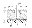
Next, the detailed structure of the
図2は、プラズマダイシングが開始される前の半導体ウェハ6を下部電極3に載置した状態を示す部分模式断面図である。半導体ウェハ6は例えばシリコンを主材質とする半導体基板であり、半導体ウェハ6の表面(図2の下面側)の回路形成面6a(第1の面)には保護シート30が貼着されている。半導体ウェハ6を下部電極3の上面である電極部3aの保持面3gの上に載置した状態では、保護シート30は保持面3gに密着することとなる。
FIG. 2 is a partial schematic cross-sectional view showing a state where the
保護シート30は、ポリイミドなどの絶縁体の樹脂を100μm程度の厚みの膜に形成した絶縁層を含んだ構成となっており、粘着材により半導体ウェハ6の回路形成面6aに剥離可能に貼り付けられる。保護シート30が貼り付けられた半導体ウェハ6を下部電極3に保持させる際には、後述するようにこの絶縁層が半導体ウェハ6を電極部3aの保持面3gによって静電吸着する際の誘電体として機能する。
The
また保護シート30の材質としては、後述のプラズマダイシングにおいて半導体ウェハ6の主材質であるシリコンよりもエッチングされにくい材質が選定されることが好ましい。
Further, as the material of the
また、回路形成面6aの反対側(図2において上側)の表面には、後述するプラズマダイシングにおける分割領域(分割線)を画定するマスクが配置されるマスク配置面6b(第2の面)となっている。このマスクは、後述するようにマスク配置面6bとなる側の表面を例えば機械加工によって研削した後に、レジスト膜31aでパターニングすることにより形成され、これによりプラズマエッチングの対象となる分割領域に相当する部分を除く領域がレジスト膜31aで覆われる。すなわち、半導体ウェハ6のマスク配置面6bにおいて、それぞれの素子形成領域に相当する部分がレジスト膜31aにて覆われ、分割領域に相当する部分にはマスク切欠部31bが配置される。
Further, on the surface opposite to the
また、図2に示すように、下部電極3には保持面3gに開口する吸着孔3eが複数設けられており、吸着孔3eは下部電極3の内部に設けられた吸引孔3cに連通している。図1に示すように、吸引孔3cはガスライン切換バルブ11を介して真空吸着ポンプ12に接続されており、ガスライン切換バルブ11はN2ガスを供給するN2ガス供給部13に接続されている。ガスライン切換バルブ11を切り換えることにより、吸引孔3cを、真空吸着ポンプ12またはN2ガス供給部13に選択的に接続させることが可能となっている。
As shown in FIG. 2, the
具体的には、ガスライン切換バルブ11により真空吸着ポンプ12が選択されて、吸引孔3cが真空吸着ポンプ12と連通された状態において真空吸着ポンプ12を駆動することにより、それぞれの吸着孔3eから真空吸引を行って下部電極3に載置された半導体ウェハ6を真空吸着して保持することができる。従って、それぞれの吸着孔3e、吸引孔3c、及び真空吸着ポンプ12は、下部電極3の保持面3gに開口したそれぞれの吸着孔3eから真空吸引することで、保護シート30を電極部3aの保持面3gに密着させた状態で、半導体ウェハ6を真空吸着により保持する真空吸着手段となっている。
Specifically, the
また、ガスライン切換バルブ11によりN2ガス供給部13が選択されて、吸引孔3cをN2ガス供給部13に接続させることにより、それぞれの吸着孔3eから保護シート30の下面に対してN2ガスを噴出させることができるようになっている。後述するようにこのN2ガスは、保護シート30を保持面3gから強制的に離脱させる目的のブロー用ガスである。
Further, when the N 2
また、図1に示すように、下部電極3には冷却用の冷媒流路3dが設けられており、冷媒流路3dは冷却装置10と接続されている。冷却装置10を駆動することにより、冷媒流路3d内を冷却水などの冷媒が循環し、これによりプラズマ処理時に発生した熱によって昇温した下部電極3や下部電極3上の保護シート30を介して半導体ウェハ6が冷却される。なお、冷媒流路3dおよび冷却装置10は、下部電極3を冷却する冷却手段となっている。
As shown in FIG. 1 , the
また、図1のプラズマ処理装置101において、処理室2に連通して設けられた排気ポート1aには、排気切換バルブ7を介して真空ポンプ8が接続されている。排気切換バルブ7を排気側に切り換えて真空ポンプ8を駆動することにより、真空チャンバ1の処理室2内部が真空排気され、処理空2内を減圧することが可能となっている。また、処理室2は圧力センサ28(図1において図示省略、図4参照)を備えており、この圧力センサ28の圧力計測結果に基づいて、後述する制御装置33(図4参照)によって真空ポンプ8が制御されることにより、処理室2内を所望の圧力に減圧することが可能とされている。なお、このような所望の圧力に減圧するための真空ポンプ8の制御は、例えば、真空ポンプ8として可変容量型のものを用いて真空ポンプ8自体の真空排気能力を直接的に制御すること、あるいは、開度調整弁(バタフライ弁等)を真空排気経路に設け、その開度を制御することで間接的に真空排気能力を制御することにより行うことができる。なお、真空ポンプ8及び排気切換バルブ7が、処理室2内を所望の圧力に減圧する真空排気装置(減圧手段)となっている。また、排気切換バルブ7を大気開放側に切り換えることにより、排気ポート1aを通して処理空2内には大気が導入され、処理室2内部の圧力を大気圧に復帰させることが可能となっている。
Further, in the
次に上部電極4の詳細構造について説明する。上部電極4は、中央の電極部4aと電極部4aを囲むようにその外周部に固定して設けられた絶縁体からなる環状部材4fを備えている。環状部材4fの内径は下部電極3の電極部4aの外径と略同じとされており、下部電極3の周面よりも外側に広がるような形状で同心配置されており、環状部材4fは、上部電極4の下方中央部に配置された円盤状のガス吹出部4eを保持する機能を担っている。
Next, the detailed structure of the
ガス吹出部4eは、上部電極4と下部電極3の間に形成される放電空間においてプラズマ放電を発生させるためのプラズマ発生用ガスを供給する。ガス吹出部4eは、内部に多数の微細孔を有する多孔質材料を円盤状に加工した部材であり、上部電極4の電極部4aの下面、ガス吹出部4eの上面、および環状部材4fの内周面にて囲まれたガス滞留空間4g内に供給されたプラズマ発生用ガスを、これらの微細孔を介して放電空間内に満遍なく吹き出させて均一な状態で供給することが可能となっている。
The
支持部4b内には、ガス滞留空間4gに連通するガス供給孔4cが設けられており、ガス供給孔4cは、真空チャンバ1の外部に配置されたプラズマ発生用ガス供給装置に接続されている。このプラズマ発生用ガス供給装置は、異なる種類のガスを個別に供給する複数のガス供給部として第1のガス供給部20A、第2のガス供給部20B、第3のガス供給部20C、及び第4のガス供給部20Dと、それぞれのガス供給部20A、20B、20C、20Dより供給されるガスを混合してガス組成を均一な状態とするガス混合部(配管の結合部)19と、このガス混合部19とそれぞれのガス供給部20A、20B、20C、20Dとの間に配置され、ガス混合部19に供給されるそれぞれのガスの供給流量を個別的に調整するガス流量調整部21とを備えている。
A
ガス流量調整部21は、第1のガス供給部20Aより供給されるガス流量を独自に調整する第1の流量制御バルブ23Aとガスの供給を遮断可能な第1の開閉バルブ22Aと、第2のガス供給部20Bより供給されるガス流量を独自に調整する第2の流量制御バルブ23Bとガスの供給を遮断可能な第2の開閉バルブ22Bと、第3のガス供給部20Cより供給されるガス流量を独自に調整する第3の流量制御バルブ23Cとガスの供給を遮断可能な第3の開閉バルブ22Cと、第4のガス供給部20Dより供給されるガス流量を独自に調整する第4の流量制御バルブ23Dとガスの供給を遮断可能な第4の開閉バルブ22Dとを備えており、それぞれのバルブの開度制御及び開閉制御は、後述する制御装置33により行われる。
The gas flow
本第1実施形態のプラズマ処理装置101においては、例えば、第1のガス供給部20Aより六フッ化硫黄ガス(SF6)が供給可能であり、第2のガス供給部20Bよりヘリウム(He)が供給可能であり、第3のガス供給部20Cより酸素(O2)が供給可能であり、第4のガス供給部20Dより三フッ化メタン(CHF3)が供給可能とされている。このようにプラズマ発生用ガス供給装置が構成されていることにより、それぞれのガス供給部20A、20B、20C、及び20Dより選択された1又は複数のガス供給部より供給されたガスの供給流量をガス流量調整部21にて個別に調整して、所望のガス組成及び流量の混合ガス(あるいは単独のガス)をガス混合部19に供給するとともに、ガス混合部19にて混合されたガス(混合ガス)を、ガス供給孔4c、ガス滞留空間4g、及びガス吹出部4eを通して放電空間内に供給することが可能となっている。
In the
また、それぞれのガスの流量を個別に調整できるというガス流量調整部21の機能を用いて、ガス組成、すなわちガスの供給比率を変更することなく、供給流量のみを変更することで、処理室2内の圧力を制御することができる。具体的には、予め設定された圧力条件と圧力センサ28により検出される処理室2内の圧力に基づいて、制御装置33によりガス流量調整部21を制御することにより、処理室2内の圧力を上記圧力条件に合致するように調整することができる。従って、ガス流量調整部21は処理室2内に供給されるガス組成を調整する機能と、処理室2内の圧力を制御する機能とを併せ持っている。
Further, by using the function of the gas flow
また、図1に示すように、下部電極3は、マッチング回路16を介して高周波電源部17に電気的に接続されている。高周波電源部17を駆動することにより、接地部9に接地された真空チャンバ1と導通した上部電極4と下部電極3の間には高周波電圧が印加される。これにより、処理室2内部では上部電極4と下部電極3との間の放電空間においてプラズマ放電が発生し、処理室2内に供給されたプラズマ発生用ガスがプラズマ状態に移行する。また、マッチング回路16は、このプラズマ発生時において処理室2内のプラズマ放電回路と高周波電源部17のインピーダンスを整合させる機能を有している。なお、本実施形態においては、高周波電源部17とマッチング回路16とが高周波電力印加装置の一例となっている。
In addition, as shown in FIG. 1, the
さらに下部電極3には、RFフィルタ15を介して静電吸着用DC電源部18が接続されている。静電吸着用DC電源部18を駆動することにより、図3(A)のプラズマ処理装置101の模式図に示すように、下部電極3の表面には負電荷(図中「−」にて示す)が蓄積される。そしてこの状態で図3(B)のプラズマ処理装置101の模式図に示すように、高周波電源部17を駆動して処理室2内にプラズマ34(図中点表示部分にて示す)を発生させると、保持面3g上に保護シート30を介して載置された半導体ウェハ6と接地部9とを接続する直流印加回路32が処理室2内のプラズマ34を介して形成される。これにより、下部電極3、RFフィルタ15、静電吸着用DC電源部18、接地部9、プラズマ34、及び半導体ウェハ6を順次結ぶ閉じた回路が形成され、半導体ウェハ6には正電荷(図中「+」にて示す)が蓄積される。
Furthermore, a DC
そして導電体により形成された下部電極3の保持面3gに蓄積された負電荷「−」と、半導体ウェハ6に蓄積された正電荷「+」との間には、誘電体としての絶縁層を含む保護シート30を介してクーロン力が作用し、このクーロン力によって半導体ウェハ6は下部電極3に保持される。このとき、RFフィルタ15は、高周波電源部17の高周波電圧が、静電吸着用DC電源部18に直接印加されることを防止する。なお、静電吸着用DC電源部18の極性は正負逆でもよい。なお、このようにプラズマ処理装置101において、実質的にプラズマの発生に寄与している構成部分をまとめて、プラズマ発生装置ということもできる。
An insulating layer serving as a dielectric is provided between the negative charge “−” accumulated on the holding
また、上記構成において、静電吸着用DC電源部18は、下部電極3に直流電圧を印加することにより、保護シート30で隔てられた半導体ウェハ6と下部電極3の保持面3gとの間に作用するクーロン力を利用して、半導体ウェハ6を静電吸着する静電吸着手段となっている。すなわち、下部電極3に半導体ウェハ6を保持させる保持手段は、保持面3gに開口する複数の吸着孔3eを介して保護シート30を真空吸着する真空吸着手段と、上述の静電吸着手段との2種類を使い分けできるようになっている。
Further, in the above configuration, the electrostatic adsorption DC
また、下部電極3と同様に上部電極4にも冷却用の冷媒流路4dが設けられており、冷媒流路4dは冷却装置10と接続されている。冷却装置10を駆動することにより、冷媒流路4d内を冷却水などの冷媒が循環し、これによりプラズマ処理時に発生した熱によって昇温した上部電極4を冷却することが可能となっている。
Similarly to the
また、処理室2の側面には、処理対象物である半導体ウェハ6の出し入れ用の開口部1bが設けられている(図13参照)。開口部1bの外側には扉開閉装置26によって昇降する扉25が設けられており、扉25を昇降させることにより開口部1bが開閉される。図13は、扉開閉装置26により扉25を下降させて開口部1bを開放した状態で半導体ウェハ6を出し入れする状態を示している。
In addition, an
また、図13に示すように、半導体ウェハ6の出し入れ時には、電極昇降装置24により上部電極4を上昇させてウェハ搬出入位置に位置させて、上部電極4と下部電極3との間に搬送用のスペースを確保する。そしてこの状態で、半導体ウェハ6を吸着保持した吸着ヘッド27を、アーム27aを操作することによって開口部1bを介して処理室2内に進入させる。これにより、下部電極3上への半導体ウェハ6の搬入および処理済みの半導体ウェハ6(半導体装置)の搬出が行われる。
As shown in FIG. 13, when the
(制御系の構成)
次にこのような構成を有するプラズマ処理装置101における制御系の構成について、図4に示す制御系のブロック図を用いて以下に説明する。
(Control system configuration)
Next, the configuration of the control system in the
図4に示すように、制御装置33は、各種のデータや処理プログラムを記憶する記憶部92と、これらのデータや処理プログラムに基づいて、プラズマ処理装置101における各構成部の動作制御を行うことでプラズマ処理の制御を行うプロセス制御部91とを備えている。記憶部92は、プラズマ処理条件81(プラズマ条件または運転条件というような場合であってもよい)や、プラズマ処理の動作プログラム82を記憶しており、プロセス制御部91は、動作プログラム82及びプラズマ処理条件81に基づいてプラズマ処理の制御を行う。操作・入力部94はキーボードなどの入力手段であり、プラズマ処理条件などのデータ入力や操作コマンドの入力を行う。表示部93はディスプレイ装置であり、操作入力時の案内画面などの表示を行う。なお、図示しないが、制御装置33が外部入出力インターフェースを備えて、装置外部との情報の受け渡しが行われるような場合であってもよい。
As shown in FIG. 4, the
ここで、本第1実施形態のプラズマ処理装置101において用いられるプラズマ処理条件について説明する。本第1実施形態において行われるプラズマ処理工程には、後述するように、プラズマダイシング工程(あるいはプラズマエッチング工程)、絶縁膜除去工程、及びマスク除去工程の大きく3つの処理工程がある。また、このようなプラズマダイシング工程においては、後述するように、プラズマエッチングの実施により絶縁膜露呈工程、角部除去工程、及び等方性エッチング工程の3つの処理工程が行われ、このようなそれぞれの処理工程を行うためのプラズマ処理条件81が予め個別に定められている。具体的には、プラズマ処理条件81は、例えば、それぞれのプラズマ発生用ガスのガス組成と、処理室2内の圧力と、上部電極4と下部電極3との間に印加される高周波の周波数(放電周波数)との組み合わせ条件により決定される。
Here, plasma processing conditions used in the
また、本第1実施形態のプラズマ処理装置101においては、上記プラズマエッチングとして、半導体ウェハ6の表面沿いの方向よりも厚み方向に強いエッチング特性(すなわち、当該厚み方向を主方向としたエッチング特性)を有する異方性エッチングと、当該表面沿いの方向と厚み方向との略等しいエッチング特性を有する等方性エッチングという互いにそのエッチング特性が異なる2種類のエッチングが用いられる。具体的には、上記プラズマダイシング工程において、上記絶縁膜露呈工程及び上記角部除去工程は、同じプラズマ処理条件にて異方性エッチングが実施されることにより行われ、上記等方性エッチング工程は、上記異方性エッチングから等方性エッチングに切り替えて実施されることにより行われる。
In the
このようなそれぞれのプラズマ処理条件81の一例を図12のデータテーブルに示す。図12に示すように、上記絶縁膜露呈工程用及び上記角部除去工程用の異方性エッチング用プラズマ処理条件81Aとしては、混合ガスのガス組成(すなわち、それぞれのガスの混合比)がSF6とO2とを10:2の比率として、圧力を100Paとし、そして周波数を60MHzとする組み合わせの条件となる。また、等方性エッチング用プラズマ処理条件81Bとしては、ガス組成がSF6とHeとを10:30の比率として、圧力を500Paとし、そして周波数を13.56MHzとする組み合わせの条件となっている。また、プラズマダイシング処理における上述以外の条件としては、上部電極4と下部電極3との間の電極間距離Dの条件があり、例えば電極間距離Dとして5〜50mmの範囲で最適と考えられる値(電極間距離D1とする)が、プラズマ処理条件81A及び81Bとして設定される。
An example of each of these plasma processing conditions 81 is shown in the data table of FIG. As shown in FIG. 12, as the anisotropic etching plasma processing conditions 81A for the insulating film exposing step and the corner portion removing step, the gas composition of the mixed gas (that is, the mixing ratio of each gas) is SF. The condition is a combination of 6 and O 2 at a ratio of 10: 2, a pressure of 100 Pa, and a frequency of 60 MHz. The plasma processing condition 81B for isotropic etching is a combination of gas composition of SF 6 and He at a ratio of 10:30, a pressure of 500 Pa, and a frequency of 13.56 MHz. . Moreover, as conditions other than the above in the plasma dicing process, there is a condition of an interelectrode distance D between the
また、絶縁膜除去処理用のプラズマ処理条件81Cとしては、例えば、後述するように、絶縁膜としてシリコン酸化膜(SiO2)が用いられるような場合には、ガス組成がCHF3を20の比率として、圧力を50Paとし、そして周波数を13.56MHzとする組み合わせの条件となっている。さらに、マスク除去処理用のプラズマ処理条件81Dとしては、ガス組成がO2を20の比率として、圧力を50Paとし、そして周波数を13.56MHzとする組み合わせの条件となっている。また、このマスク除去処理用のプラズマ処理条件81Dには、その他、例えば電極間距離Dが50〜100mmの範囲内で最適と考えられる値(電極間距離D2とする)が設定されている。また、それぞれのプラズマ処理条件81には、処理実施時間の条件が含まれている。 Further, as the plasma processing condition 81C for the insulating film removal processing, for example, as described later, when a silicon oxide film (SiO 2 ) is used as the insulating film, the gas composition has a CHF 3 ratio of 20. The pressure is 50 Pa and the frequency is 13.56 MHz. Further, the plasma processing conditions 81D for the mask removal processing are a combination of the gas composition with a ratio of O 2 of 20, a pressure of 50 Pa, and a frequency of 13.56 MHz. In addition, in the plasma processing condition 81D for the mask removal processing, a value (referred to as an interelectrode distance D2) that is considered to be optimal when the interelectrode distance D is within a range of 50 to 100 mm, for example, is set. In addition, each plasma processing condition 81 includes a processing execution time condition.
また、上記プラズマダイシング工程における異方性エッチングと等方性エッチングとの切り替え、すなわちエッチング特性の切り替えは、上述のようにガス組成、圧力、及び周波数の組み合わせにより決定されるプラズマ処理条件81Aとプラズマ処理条件81Bとを切り替えることにより行うことが好ましいが、このような条件の切り替えのみに限られるものではない。このような場合に代えて、例えば、ガス組成、圧力、及び周波数のうちのいずれか1つのパラメータのみを切り換えるような場合であっても、エッチング特性の切り換えを行うことができる。このようなエッチング特性の切り換えにおいては、ガス組成が最も有効なパラメータであり、その次に、圧力、そして周波数の順序となる。例えば、ガス組成のみを変更することで上記エッチング特性の切り換えを行うような場合にあっては、SF6:O2:Heのガス組成を、10:2:0から10:0:30と変更することで、異方性エッチングから等方性エッチングへの切り替えを行うことができる。また、処理室2内の圧力のみを変更することで上記エッチング特性の切り替えを行うような場合にあっては、圧力を上昇させる(例えば、100Paから500Paとする)ことで、異方性エッチングから等方性エッチングへの切り換えを行うことができる。また、高周波の周波数のみを変更することで上記エッチング特性の切り換えを行うような場合にあっては、周波数を低くする(例えば、60MHzから13.56MHzとする)ことで、異方性エッチングから等方性エッチングへの切り換えを行うことができる。なお、これらのパラメータの他にも、例えば、高周波出力(例えば、500〜3000Wの範囲で設定される)やガス供給流量も一のパラメータとして用いられる。
In addition, switching between anisotropic etching and isotropic etching in the plasma dicing process, that is, switching of etching characteristics, is performed by plasma processing conditions 81A and plasma determined by a combination of gas composition, pressure, and frequency as described above. This is preferably performed by switching the processing condition 81B, but is not limited to switching such a condition. Instead of such a case, for example, even when only one parameter of the gas composition, pressure, and frequency is switched, the etching characteristics can be switched. In such etching characteristics switching, the gas composition is the most effective parameter, followed by pressure and frequency. For example, in the case where the etching characteristics are changed by changing only the gas composition, the gas composition of SF 6 : O 2 : He is changed from 10: 2: 0 to 10: 0: 30. By doing so, switching from anisotropic etching to isotropic etching can be performed. Further, in the case where the etching characteristics are switched by changing only the pressure in the
また、異方性エッチング用のガス組成としては、デポジション(deposition:蒸着又は堆積)しやすい反応生成物を生じるようなガス組成を用いることが好ましい。例えば、異方性エッチング用のガス組成として、酸素を含むガス組成を用いることで、反応生成物としてシリコンのフッ素酸化物(SixFyOz)を生成することができる(ここで、x、y、zは整数である)。このフッ素酸化物は、シリコンよりもエッチングされ難いという特性を有している。このような特性を利用することで、半導体ウェハにおいて、異方性エッチングの実施によりその表面に溝部を形成するとともに、当該形成された溝部の内側面に生成されたフッ素酸化物を付着させて膜を形成することができる(側壁デポジション)。一方、加速されたイオンによる物理的エッチングにより、上記溝部の底面にはフッ素酸化物が付着し難い。これにより、上記溝部の内側面は底面に比べてエッチングされ難くすることができ、その結果として当該エッチングを半導体ウェハの厚み方向に強く行うことが可能となり、より理想に近い異方性エッチングを実現することができる。従って、異方性エッチング用のガス組成としては、異方性エッチングを促進させるようなガス組成、すなわち側壁デポジションを起こし易いガス組成を用いることが好ましい。 Moreover, as a gas composition for anisotropic etching, it is preferable to use a gas composition that generates a reaction product that is easily deposited (deposition: vapor deposition or deposition). For example, by using a gas composition containing oxygen as a gas composition for anisotropic etching, fluorine oxide (Si x F y O z ) of silicon can be generated as a reaction product (where x x , Y and z are integers). This fluorine oxide has a characteristic that it is harder to etch than silicon. By utilizing these characteristics, a groove is formed on the surface of a semiconductor wafer by anisotropic etching, and a fluorine oxide generated on the inner surface of the formed groove is attached to the film. Can be formed (side wall deposition). On the other hand, it is difficult for fluorine oxide to adhere to the bottom surface of the groove due to physical etching with accelerated ions. As a result, the inner surface of the groove portion can be made harder to etch than the bottom surface, and as a result, the etching can be strongly performed in the thickness direction of the semiconductor wafer, realizing a more ideal anisotropic etching. can do. Therefore, as the gas composition for anisotropic etching, it is preferable to use a gas composition that promotes anisotropic etching, that is, a gas composition that easily causes sidewall deposition.
また、このような異方性エッチング用のプラズマ処理条件81A、等方性エッチング用のプラズマ処理条件81B、絶縁膜除去処理用のプラズマ処理条件81C、及びマスク除去処理用のプラズマ処理条件81Dのそれぞれは、制御装置33の記憶部92に記憶されており、動作プログラム82に基づいて、工程毎に必要なプラズマ処理条件81が選択されて、プロセス制御部91により、当該選択されたプラズマ処理条件81に基づいて、プラズマ処理が行われる。
Further, each of the plasma processing conditions 81A for anisotropic etching, the plasma processing conditions 81B for isotropic etching, the plasma processing conditions 81C for insulating film removal processing, and the plasma processing conditions 81D for mask removal processing, respectively. Is stored in the
動作プログラム82に基づいて行われるプラズマ処理においては、図4に示すように、ガス流量調整部21、ガスライン切換バルブ11、高周波電源部17、静電吸着用DC電源部18、排気切換バルブ7、真空ポンプ8、真空吸着ポンプ12、扉開閉装置26、及び電極昇降装置24の各部が、プロセス制御部91により制御される。
In the plasma processing performed based on the
また、圧力センサ28の圧力検出結果に基づいて、プロセス制御部91のよりガス流量調整部21が制御されてそれぞれのガスの供給量の総量が調整されることで、処理室2の内部の圧力を、プラズマ処理条件81に合致させるように制御することができる。
Further, based on the pressure detection result of the
さらに、図4に示すように、制御装置33には、プラズマ処理時間の計測を行う処理時間計測部95が備えられており、プラズマ処理の処理時間の計測を行い、当該計測結果が、例えば、それぞれのプラズマ処理条件81に含まれている処理時間の条件に到達したときに、プロセス制御部91により当該処理を終了させるような制御を行うことが可能となっている。
Furthermore, as shown in FIG. 4, the
次に、本第1実施形態において用いられるプラズマエッチング処理方法の原理について、図5及び図6に示す半導体ウェハ6における分割領域付近の部分拡大模式説明図を用いて以下に説明する。
Next, the principle of the plasma etching method used in the first embodiment will be described below with reference to partially enlarged schematic explanatory views in the vicinity of the divided regions in the
図5は、回路形成面6aに保護シート30が貼着され、マスク配置面6bに分割領域を画定するようにレジスト膜31aが配置された半導体ウェハ6において、マスク配置面6b側よりマスク切欠部31bに相当、すなわち分割領域に相当する部分に対して、プラズマエッチング処理を施している状態を示す図である。また、図5に示すように、本第1実施形態において用いられる半導体ウェハ6は、その回路形成面6aにおいて、絶縁膜の一例であって酸化シリコン(SiO2)により形成されたシリコン酸化膜35が分割領域の相当する部分にも形成されているような半導体ウェハであり、分割領域に相当する部分においてこのようなシリコン酸化膜が形成されていない従来の半導体ウェハとは異なる構成を有している。なお、このように形成されたシリコン酸化膜35側の回路形成面6aに保護シート30が貼着されている。
FIG. 5 shows a mask notch portion from the
図5に示すように、プラズマ中のイオンは、プラズマ処理装置101において発生される電界によって、半導体ウェハ6に対して略垂直に入射し、エッチング加工により形成された溝部の底部(エッチング底部)に当該入射したイオンが到達してエッチングが促進される。このようにエッチング底部に到達したイオン(正電荷を有する)は、半導体材料であるシリコンにより形成されている半導体ウェハ6中の電子と再結合する。すなわち、シリコン材料は導電体としての特性も兼ね備えているため、エッチング底部と半導体ウェハ6の内部との導通により、エッチング底部に到達して正電荷を有するイオンと、半導体ウェハ6中の電子との再結合が行われ、このような導通が行われる限り、エッチング底部には正電荷が蓄積されることはない。
As shown in FIG. 5, ions in the plasma are incident substantially perpendicularly to the
一方、図6に示すように、エッチングが進行して、エッチング底部が除去され、シリコン酸化膜35の表面が露呈された状態とされると、当該露呈されたシリコン酸化膜35と半導体ウェハ6中とは、酸化シリコンが絶縁材料であることにより導通されないため、到達したイオンにより露呈されたシリコン酸化膜35上には正電荷がチャージアップ(帯電)されて正電荷が蓄積されることとなる。このように露呈されたシリコン酸化膜35が正電荷に帯電された状態とされると、次に入射してくるイオンが、正電荷同士の電界により直進性を失い、その軌道が曲げられてしまうこととなる。その結果、図6に示すように、溝部における両隅部分にイオンが到達されることとなり、当該両隅部分においてエッチングが行われ、溝部がその底部において幅方向に急激に拡大されたノッチと呼ばれる形状の切り欠き部が形成される。これが本第1実施形態において用いられるプラズマエッチング処理方法の原理である。
On the other hand, as shown in FIG. 6, when the etching proceeds, the bottom of the etching is removed, and the surface of the
このように溝部の底部においてノッチを形成することで、エッチングされる側である半導体ウェハ6側から見れば、分割された半導体チップの角部の除去、例えば湾曲凸面部であるR(アール)部の形成を行うことができる(角部除去工程)。また、このようなプラズマ処理方法の原理は、図5に示す状態、すなわち、シリコン酸化膜35が露呈されていない状態において、照射されるプラズマ中のイオンがエッチング底部により到達し易いように、異方性エッチングが行われることが好ましく、本第1実施形態においても絶縁膜露呈工程において異方性エッチングを行うものとしている。また、このようなプラズマダイシング処理において、シリコン酸化膜35を露呈させるまでに要する処理時間(すなわち絶縁膜露呈工程の処理時間)と、シリコン酸化膜35が露呈されてから所定の大きさのノッチを形成(すなわち、面取りやR部形成等、角部の除去)するために必要な処理時間(すなわち角部除去工程の処理時間)は、異方性エッチング用のプラズマ処理条件81Aに含まれている。
In this way, by forming a notch at the bottom of the groove portion, when viewed from the side of the
(半導体チップの製造方法)
次に、このような構成を有するプラズマ処理装置101を用いて行われる半導体チップの製造方法およびこの半導体チップの製造方法の過程において実行される半導体ウェハの分割方法(プラズマダイシング処理)について、以下に説明する。また、半導体ウェハの分割方法おける一連の手順を示すフローチャートを図7に示し、さらに、半導体チップの製造方法における一連の処理内容を説明するための模式説明図を図8(A)〜(C)、図9(A)〜(C)、図10(A)〜(C)、及び図11(A)、(B)に示し、これらの図面を主に参照しながら以下に説明を行う。
(Semiconductor chip manufacturing method)
Next, a semiconductor chip manufacturing method performed using the
半導体ウェハ6は円盤形状を有しており、その回路形成面6aには複数の素子形成領域R1が格子状に配列されている。それぞれの素子形成領域R1は、製造される半導体チップの大きさに応じてその大きさが決定されており、例えば方形状の領域として配置されている。このような半導体ウェハ6の部分拡大模式断面図を図8(A)に示す。図8(A)に示すように、互いに隣接する素子形成領域R1の間には、所定の幅寸法を有する大略帯状の領域(すなわちその長手方向に比して十分に小さな幅寸法を有する領域)である分割領域R2が配置されている。この分割領域R2は、半導体ウェハ6の回路形成面6aにおいて略格子状に配列されているとともに、それぞれの素子形成領域R1を画定する領域となっており、1つの素子形成領域R1との関係では、当該素子形成領域R1の外周に配置された枠形状の領域となっている。さらに、この分割領域R2は、プラズマダイシング工程において、それぞれの素子形成領域R1を個別に分割するための分割位置となっている。また、それぞれの素子形成領域R1内には、半導体素子44が形成されている。
The
具体的には、図8(A)に示すように、半導体ウェハ6は、円盤形状を有するシリコン基板45により形成されており、その回路形成面6a全体には、SiO2により形成されたシリコン酸化膜35が形成されている。さらに、回路形成面6aにおけるそれぞれの素子形成領域R1に相当する部分には、半導体素子44が形成されている。半導体素子44は、シリコン基板45(Semiconductor)と、回路形成面6a上に直接的に形成されたシリコン酸化膜35(Oxide)と、このシリコン酸化膜35上に形成された金属膜(Metal)とで構成されるMOS(Metal−Oxide−Semiconductor)構造トランジスタ等のデバイス群を含んでいる。さらに、半導体素子44は、デバイス群を外部の電子装置と電気的に接続する為の接続端子43(ボンディングパッドとも呼ぶ)も備えている。なお、それぞれの半導体素子44の表面には、表面保護膜46(例えば、ポリイミドにて形成される)が形成され、半導体素子44の表面の保護が行われている。接続端子43は表面保護膜35で覆われず外部に露呈している。
Specifically, as shown in FIG. 8A, the
このような半導体ウェハ6に対して、図8(B)に示すように、以降において行われるそれぞれの処理の際に回路形成面6aが損傷を受けることが無いように、回路形成面6aに保護シート30が粘着剤を介して剥離可能に貼着される。なお、保護シート30は、回路形成面6aの全面を覆い且つ半導体ウェハ6から外側にはみ出すことのないよう、半導体ウェハ6の外形形状と同じ形状に整形したものが用いられる。このような形状の保護シート30が用いられることにより、その後の処理、例えばプラズマ処理において、半導体ウェハ6からはみ出した保護シート30がプラズマによって損傷するというダメージの発生を防止することができる。
For such a
次に、図8(C)に示すように、半導体ウェハ6の回路形成面6aの裏面であるマスク配置面6bに、半導体ウェハ6を半導体チップの個片に分割するための分割領域R2を画定するマスクを形成する。具体的には、当該マスクとして例えば樹脂より成るレジスト膜31を半導体ウェハ6のマスク配置面6bの全面を覆うように形成する。その後、図9(A)に示すように、レジスト膜31をフォトリソグラフィによってパターニングして、分割領域R2に相当する部分のみを例えば20μm幅で除去して、マスク切欠部31bを形成する。これにより、半導体ウェハ6のマスク配置面6bには、それぞれの素子形成領域R1に相当する部分をレジスト膜31aによって覆い、かつ、分割領域R2に相当する部分をマスク切欠部31bにより露出させるようなマスクパターンが形成される。この状態のマスク付きの半導体ウェハ6が、後述するプラズマ処理の対象となる。
Next, as shown in FIG. 8C, a division region R2 for dividing the
以下、このマスク付きの半導体ウェハ6に対してプラズマ処理を行うことで、半導体チップの個片へと分割する方法について、図7のフローチャートに沿って、図13から図15に示すプラズマ処理装置101の模式図を参照しながら説明する。なお、プラズマ処理装置101における以降のそれぞれの動作の制御は、制御装置33の記憶部92内に保持されている動作プログラム82に基づいて、プロセス制御部91により各構成部が制御されることにより行われる。
Hereinafter, a
まず、図7のフローチャートのステップS1において、図13に示すように、マスク付きの半導体ウェハ6が処理室2内に搬入される。この搬入動作に際しては、上部電極4を電極昇降装置24によって上昇させた状態で、アーム27aを操作して、吸着ヘッド27にマスクを介して保持された半導体ウェハ6を開口部1bから処理室2内に搬入し、半導体ウェハ6を下部電極3上に保護シート30を介して載置する。
First, in step S1 of the flowchart of FIG. 7, the
次に、真空吸着ポンプ12を駆動してそれぞれの吸着孔3eから真空吸引し、半導体ウェハ6の真空吸着をON状態にするとともに、静電吸着用DC電源部18をON状態にする(ステップS2)。この真空吸着により、処理室内2において保護シート30を下部電極3の保持面3gに密着させた状態で、半導体ウェハ6を下部電極3によって保持する。
Next, the
この後、図14に示すように扉25が閉じられ、電極昇降装置24により上部電極4を下降させる(ステップS3)。このとき、制御装置33において、記憶部92に保持されているそれぞれのプラズマ処理条件81の中から、動作プログラム82に基づいてプロセス制御部91により異方性エッチング用のプラズマ処理条件81Aが選択されて取り出されるとともに、この異方性エッチング用のプラズマ処理条件81Aに含まれる電極間距離Dの条件に基づいて、上部電極4と下部電極3との間の電極間距離Dが例えば5〜50mmの範囲内の所定の条件(すなわち、電極間距離D1)に設定される。
Thereafter, as shown in FIG. 14, the
次いで真空ポンプ8を作動させ、処理室2内の減圧を開始する(ステップS4)。処理室2内が所定の真空度に到達したならば、上記選択された異方性エッチング用プラズマ処理条件81Aに基づいて、ガス流量調整部21により選択されたガスが所定のガス組成かつ所定の流量に調整されて処理室2内に供給される(ステップS5)。具体的には、異方性エッチング用プラズマ処理条件81Aに基づいて、第1の開閉バルブ22Aが開放されて、第1のガス供給部20AからSF6が第1の流量制御バルブ23Aによりその供給流量が調整されてガス混合部19に供給されるとともに、第3の開閉バルブ部22Cが開放されて、第3のガス供給部20CからO2が第3の流量制御バルブ23Cによりその供給流量が調整されてガス混合部19に供給される。なお、このとき、第2の開閉バルブ22B及び第4の開閉バルブ22Dは閉止された状態とされ、He及びCHF3の供給は行われない。また、ガス混合部19において、SF6とO2とが10:2のガス組成となるように混合されて、処理室2内に供給される。
Next, the
そしてガス供給過程において、処理室2内の圧力を圧力センサ28により検出してプラズマ処理条件81Aの中の圧力条件(例えば、100Pa)と比較し、当該検出された圧力が当該圧力条件に示す圧力に到達したことを確認する。すなわち、下部電極3と上部電極4との電極間距離D、処理室2に供給されるガス組成、ならびに処理室2内の圧力が、異方性エッチング用プラズマ処理条件81Aに基づいて設定される。
In the gas supply process, the pressure in the
そして上記条件設定が完了した後、プラズマ処理条件81Aの高周波の周波数(例えば、60MHz)及び出力条件に基づいて、高周波電源部18を駆動して上部電極4と下部電極3との間に、当該条件に合致する高周波電圧を印加し、プラズマ放電を開始する(ステップS6)。これにより、上部電極4と下部電極3との間の放電空間において、供給された混合ガスをプラズマ状態に移行させる。このプラズマ発生により、当該プラズマ中のイオンがマスク側(レジスト膜31a側)から半導体ウェハ6に照射される。このイオンの照射により、半導体ウェハ6の主材質であるシリコン(すなわちシリコン基板45)のうち、レジスト膜31aに覆われていない分割領域R2に相当する部分のみがエッチングされる。
After the above condition setting is completed, the high frequency
これとともに、プラズマによって上部電極4と下部電極3との間の放電空間には直流印加回路32が形成される(図3(A)及び(B)参照)。これにより、下部電極3と半導体ウェハ6との間には静電吸着力が発生し、半導体ウェハ6は下部電極3に静電吸着力により保持される。このため保護シート30は下部電極3の保持面3gに良好に密着し、半導体ウェハ6はプラズマ処理過程において安定して保持されるとともに、下部電極3に備えられた冷却機能によって保護シート30が良好に冷却され、プラズマ放電によって発生する熱によるダメージが防止される。
At the same time, a
また、この異方性エッチングによるプラズマダイシング処理(絶縁膜露呈工程)においては、プラズマ処理条件81Aに基づいて異方性エッチングが行われるため、そのエッチング特性は、半導体ウェハ6の厚み方向に大きくなる。従って、図9(B)に示すように、それぞれのマスク切欠部31bに相当する半導体ウェハ6の表面を、その厚み方向にエッチングを行い、このマスク切欠部31bの幅、すなわち分割領域R2の幅に略相当するような幅の溝部6cが形成される。
Further, in the plasma dicing process (insulating film exposing process) by the anisotropic etching, the anisotropic etching is performed based on the plasma processing condition 81A, so that the etching characteristics increase in the thickness direction of the
また、ステップS7において、この溝部6cの底部であるエッチング底部がエッチングにより除去されて、当該底部よりシリコン酸化膜35の表面が露呈(すなわち絶縁膜の表面が露呈)するまで、例えば、処理時間計測部95により計測された時間が、プラズマ処理条件81Aに含まれるシリコン酸化膜35を露呈させるまでに要する処理時間の条件に到達するまで、ステップS6のプラズマダイシング処理(絶縁膜露呈工程)が行われる。このように溝部6cにおいてシリコン酸化膜35が露呈された状態とされることで、シリコン基板45において、分割領域R2に相当する部分が除去される。
In step S7, for example, the processing time measurement is performed until the etching bottom, which is the bottom of the
ステップS7において、当該所定時間に到達したものと判断された場合には、ステップS8において、ノッチ形成を行うためのプラズマダイシング処理(すなわち、ノッチ形成工程あるいは角部除去工程)として、同じ条件下での異方性エッチングによるプラズマダイシング処理がそのまま継続して行われる。これにより、プラズマ中より溝部6cの底部に向けて照射されたイオンの正電荷が、上記露呈されたシリコン酸化膜35を帯電させ、その結果、次に溝部6c内の入射してくるイオンの軌道が曲げられて、溝部6cの底部においてその幅方向に拡大されるように、分割されたシリコン基板45のエッチングが行われる。その結果、図9(C)に示すように、溝部6cの底部における両隅部分にノッチ42が形成、すなわち、分割されたそれぞれのシリコン基板45におけるシリコン酸化膜35に接する部分の角部が除去されてR(アール)部40aが形成されることとなる。
When it is determined in step S7 that the predetermined time has been reached, in step S8, plasma dicing processing for performing notch formation (that is, notch formation process or corner removal process) is performed under the same conditions. The plasma dicing process by anisotropic etching is continuously performed as it is. As a result, the positive charge of the ions irradiated from the plasma toward the bottom of the
なお、ステップS9において、所定の大きさのノッチ42やR部40aが形成されるまで、例えば、処理時間計測部95により計測された時間が、プラズマ処理条件81Aに含まれる所定の大きさのノッチを形成するために必要な処理時間の条件に到達するまで、ステップS8のノッチ形成のためのプラズマダイシング処理が行われる。
In step S9, for example, the time measured by the processing
ステップS9において、当該処理時間が到達したものと判断された場合には、異方性エッチングによるプラズマダイシング処理(ノッチ形成工程)を終了させるとともに、プロセス制御部91により等方性エッチング用のプラズマ処理条件81Bが選択されて、当該条件に基づいて、ガス流量調整部21により選択されたガスが所定のガス組成かつ所定の流量に調整されて処理室2内に供給される(ステップS10)。具体的には、等方性エッチング用プラズマ処理条件81Bに基づいて、第1の開閉バルブ22Aが開放されて、第1のガス供給部20AからSF6が第1の流量制御バルブ23Aによりその供給流量が調整されてガス混合部19に供給されるとともに、第2の開閉バルブ部22Bが開放されて、第2のガス供給部20BからHeが第2の流量制御バルブ23Bによりその供給流量が調整されてガス混合部19に供給される。なお、このとき、第3の開閉バルブ22C及び第4の開閉バルブ22Dは閉止された状態とされ、O2及びCHF3の供給は行われない。また、ガス混合部19において、SF6とHeとが10:30のガス組成となるように混合されて、処理室2内に供給される。
If it is determined in step S9 that the processing time has been reached, the plasma dicing process (notch forming process) by anisotropic etching is terminated, and the
そしてガス供給過程において、圧力センサ28により検出される処理室2内の圧力がプラズマ処理条件81Bの中の圧力条件(例えば、500Pa)に到達したことを確認する(ステップS10)。なお、下部電極3と上部電極4との電極間距離D1はそのままの状態に保たれる。
In the gas supply process, it is confirmed that the pressure in the
その後、プラズマ処理条件81Bの高周波の周波数(例えば13.56MHz)及び出力条件に基づいて、高周波電源部18を駆動して上部電極4と下部電極3との間に、当該条件に合致する高周波電圧を印加し、プラズマ放電を開始することで、等方性エッチングによるプラズマダイシング処理を開始する(ステップS11)。
After that, based on the high frequency (for example, 13.56 MHz) and the output condition of the plasma processing condition 81B, the high frequency
この等方性エッチングは、半導体ウェハ6の表面沿いの方向のエッチング特性と、厚み方向のエッチング特性とが略同じであるという特徴を有していることにより、プラズマが照射される部分においては、上記それぞれの方向に略均等にエッチングが施されることとなる。ただし実際には、等方性エッチングにおいても厚み方向のエッチング特性が表面沿いの方向のエッチング特性よりもやや強くなる傾向にあるが、上記異方性エッチングとは明らかに異なるエッチング特性を示すことには変わりはない。
This isotropic etching has the characteristics that the etching characteristics in the direction along the surface of the
このように等方性エッチングを用いたプラズマダイシング処理が行われると、図10(A)に示すように、上記異方性エッチングによるプラズマダイシング処理により形成されたそれぞれの溝部6cは、その入口付近(すなわち図示上方付近)において半導体ウェハ6の表面沿いの方向にエッチングが施されることとなる。従って、それぞれの溝部6cは、その幅方向にやや拡大されるように、エッチングが施されることとなる。また、エッチング特性は、それぞれの溝部6cの上部である入口付近程強く、底部へ行くに従って弱くなる傾向にある。従って、このような等方性エッチングを施すことにより、図10(A)に示すように、それぞれの素子形成領域R1のマスク配置面6bにおいて、分割領域R2に接する端部に湾曲凸面部であるR(アール)部40bを形成することができる。すなわち、それぞれの素子形成領域R1のマスク配置面6b側に位置される端部(角部分)及びその矩形状平面の四隅部のそれぞれにR部40bが形成される。
When the plasma dicing process using isotropic etching is performed as described above, as shown in FIG. 10A, each
なお、ステップS12において、それぞれのR部40bが所定の大きさに形成されるまで、例えば、処理時間計測部95により計測された時間が、等方性エッチング用プラズマ処理条件81Bの処理時間の条件を経過するまで、ステップS11の等方性エッチングによるプラズマダイシング処理が行われる。
In step S12, for example, the time measured by the processing
ステップS12において、当該所定時間を経過したものと判断された場合には、等方性エッチングによるプラズマダイシング処理を終了する。それとともに、プロセス制御部91により絶縁膜除去処理用のプラズマ処理条件81Cが選択されて、当該条件に基づいて、ガス流量調整部21により選択されたガスが所定のガス組成かつ所定の流量に調整されて処理室2内に供給される(ステップS13)。具体的には、絶縁膜除去処理用プラズマ処理条件81Cに基づいて、第4の開閉バルブ22Dが開放されて、第4のガス供給部20DからCHF3が第4の流量制御バルブ23Dによりその供給流量が調整されてガス混合部19に供給される。
If it is determined in step S12 that the predetermined time has elapsed, the plasma dicing process by isotropic etching is terminated. At the same time, the plasma control condition 81C for the insulating film removal process is selected by the
そしてガス供給過程において、圧力センサ28により検出される処理室2内の圧力がプラズマ処理条件81Cの中の圧力条件(例えば、50Pa)に到達したことを確認する。なお、下部電極3と上部電極4との電極間距離D1はそのままの状態に保たれる。
In the gas supply process, it is confirmed that the pressure in the
その後、プラズマ処理条件81Cの高周波の周波数(例えば、13.56MHz)及び出力条件に基づいて、高周波電源部18を駆動して上部電極4と下部電極3との間に、当該条件に合致する高周波電圧を印加し、プラズマ放電を開始することで、それぞれの溝部6cにおいて露呈された状態のシリコン酸化膜35を除去するためのプラズマエッチングを開始する(ステップS14、絶縁膜除去工程)。
After that, based on the high frequency (for example, 13.56 MHz) and the output condition of the plasma processing condition 81C, the high frequency
このようなプラズマエッチングが行われることにより、図10(B)に示すように、上記露呈されていたシリコン酸化膜35、すなわち、分割領域R2に相当する部分におけるシリコン酸化膜35に対して積極的にエッチングが行われて、当該部分におけるシリコン酸化膜35が除去される。その結果、半導体ウェハ6において、分割領域R2に相当する部分が完全に除去されて、それぞれの素子形成領域R1が個片に分割され、半導体素子44を含むそれぞれの半導体チップ40が形成されることとなる。なお、このようなプラズマエッチングは、処理時間計測部95により計測された時間が、プラズマ処理条件81Cに含まれる処理時間に到達するまで行われる(ステップS15)。
By performing such plasma etching, as shown in FIG. 10B, the exposed
ステップS15において、当該所定時間に到達したものと判断されると、この絶縁膜除去処理のためのプラズマエッチング処理、すなわち絶縁膜除去工程を終了する。当該処理終了の際には、混合ガスの供給や高周波電圧の印加が停止されることとなる。その後、プラズマアッシング工程(マスク除去工程)に移行するための電極間距離変更をおこなう(ステップS16)。具体的には、プロセス制御部91によりマスク除去処理用のプラズマ処理条件81Dが選択されて、当該条件に基づいて、図15に示すように電極昇降装置24により上部電極4を上昇させて、上部電極4と下部電極3との間の電極間距離を電極間距離D2に設定する。このようなプラズマアッシングによりマスク除去を行う際の電極間距離D2は、上述のプラズマダイシング処理における電極間距離D1よりも広く設定するようにしている。
If it is determined in step S15 that the predetermined time has been reached, the plasma etching process for the insulating film removing process, that is, the insulating film removing process is ended. At the end of the process, the supply of the mixed gas and the application of the high-frequency voltage are stopped. Thereafter, the inter-electrode distance is changed to shift to the plasma ashing process (mask removal process) (step S16). Specifically, a plasma processing condition 81D for mask removal processing is selected by the
その後、プラズマ処理条件81Dに基づいて第3のガス供給部20Cが選択されて当該第3のガス供給部20Cからプラズマアッシング用ガス(例えば、酸素)を、そのガス供給流量を調整しながら供給する(ステップS17)。そしてガス供給過程において処理室2内のガス圧力を検出して上記プラズマ処理条件と比較し、当該圧力が上記条件に示す圧力に到達したことを確認する。
Thereafter, the third gas supply unit 20C is selected based on the plasma processing condition 81D, and plasma ashing gas (for example, oxygen) is supplied from the third gas supply unit 20C while adjusting the gas supply flow rate. (Step S17). Then, in the gas supply process, the gas pressure in the
その後、高周波電源部18を駆動して上部電極4と下部電極3との間に高周波電圧を印加し、プラズマ放電を開始する(ステップS18)。これにより、上部電極4と下部電極3との間の放電空間において、供給されたガスをプラズマ状態に移行させる。このようにして発生したプラズマが、半導体ウェハ6のマスク配置面6b側に作用することにより、有機物よりなるレジスト膜31aはプラズマによってアッシング(灰化)される。
Thereafter, the high frequency
そしてこのアッシングが進行することにより、レジスト膜31aが徐々に消滅し、最終的には、図10(C)に示すように半導体ウェハ6、すなわち個片化されたそれぞれの半導体チップ40のマスク配置面6aからマスクが完全に除去される。このマスク除去工程における高周波電源の出力は、プラズマ処理条件81Dに基づいて、例えば100〜1000Wの範囲で設定された所定の値とされる。そしてマスクが完全に除去された後、プラズマ放電を停止する。
As the ashing progresses, the resist
その後、真空ポンプ8の作動を停止し(ステップS19)、排気切換バルブ7を切り換えて大気開放を行う(ステップS20)。これにより、処理室2内の圧力が大気圧に復帰する。そして真空吸着をOFF状態にするとともに、静電吸着用DC電源をOFFにする(ステップS21)。これにより、それぞれの半導体チップ40の個片に分割され、かつ保護テープ30に保持された状態の半導体ウェハ6の吸着保持が解除される。
Thereafter, the operation of the
さらにその後、プラズマ処理後の半導体ウェハ6の搬出が行われる(ステップS22)。すなわち、吸着孔3eからN2ガスをブローしながら、吸着ヘッド27によって半導体ウェハ6を吸着保持して処理室2の外へ搬出する。これにより、プラズマ処理装置101において、絶縁膜露呈工程、ノッチ形成工程、等方性エッチング工程、絶縁膜除去処理、及びマスク除去工程の各工程を連続して行うプラズマ処理が終了する。
Thereafter, the
そして、保護シート30とともに搬出された半導体ウェハ6は、シート剥離工程に送られ、それぞれの半導体チップ40の回路形成面6aから、保護シート30を剥離する。このシート剥離は、図11(A)及び(B)に示すように、保持用の粘着シート37をそれぞれの半導体チップ40のマスク配置面6bに貼り付けてそれぞれの半導体チップ40を粘着シート37に保持させた後に行われる。これにより半導体チップの製造工程が完了する。
And the
ここで、このように形成された半導体チップ40の外観を示す模式斜視図(一部切り欠き断面あり)を図30に示す。図30に示すように、半導体チップ40においては、その回路形成面6a側のそれぞれの端部(すなわち、四方向全ての端部)において、鋭利であった角部分(あるいは稜線)を除去するように、湾曲凸面部であるR部40aを形成することができる。さらに、それぞれの半導体チップ40において、そのマスク配置面6bのそれぞれの端部(すなわち四方向全ての端部)において、鋭利であった角部分(あるいは稜線)を除去するように、湾曲凸面部であるR部40bを形成することができる。すなわち、半導体チップ40において、全ての角部や稜線を除去することができる。これにより、製造された半導体チップ40において、角部等の欠けによるチッピングの発生を抑制することができ、その抗折強度を向上させることができる。
Here, FIG. 30 shows a schematic perspective view (with a partially cutaway cross section) showing the appearance of the
また、このように形成される半導体チップ40は、例えば、その幅寸法に対して、その厚み寸法が十分に小さいような薄型化された半導体チップであり、このような半導体チップ40の構造を具体的に述べると、半導体チップ40は、略方形状かつ平坦な表面であり半導体素子44が形成された第1の面(回路形成面)40cと、この第1の面40cの反対側に、当該第1の面40cと平行に配置された略方形状かつ平坦な表面である第2の面40dと、この第1の面40c及び第2の面40dの周囲に配置され、第1の面40cの端部と第2の面40dの端部とを接続する接続面40eとを備えている。さらにこの半導体チップ40においては、第1の面40c及び第2の面40dのそれぞれの端部に稜線が形成されることが無いように、接続面40eに上記湾曲凸面部であるそれぞれのR部40a及び40bが含まれて構成されている。従って、製造された半導体ウェハ40において、従来の製造方法により稜線が位置されていた部分を、湾曲凸面部にて構成することができ、その抗折強度を向上させることができる形状とすることができる。なお、上述のように半導体チップ40において、その厚み寸法が幅寸法に対して十分に小さいことを考慮すれば、接続面40eを全て湾曲凸面部にて形成することも可能である。
Further, the
また、図31の模式説明図に示すように、半導体ウェハ6のマスク配置面6bに配置される平面的に略方形状のそれぞれのレジスト膜31aの四隅部分に、凸状湾曲部すなわちR部31cを形成するような場合にあっては、形成される半導体チップ40の形状をさらに滑らかな形状とすることができ好適である。なお、このように形成される半導体チップ40においては、例えば、分割領域R2の幅寸法が5〜20μm程度であり、除去される角部の幅寸法、すなわちR部40a及び40bの径寸法が0.5〜20μm程度であり、さらに除去されるシリコン酸化膜35の幅寸法が50μm以下程度となっている。ただし、「R部」、すなわち「湾曲凸面部」の曲率が限りなく小さくなれば、当該湾曲凸面部は限りなく面取り部(傾斜平面部あるいはテーパ部)に近い形状となるが、僅かでも湾曲された凸面部である限り、このような面取り部は本実施形態の湾曲凸面部に含まれるものである。
Further, as shown in the schematic explanatory view of FIG. 31, convex curved portions, that is,
なお、上記説明においては、半導体チップ40の角部分にノッチ形成によりR部40aが形成されるような場合について説明したが、本第1実施形態の半導体チップの製造方法はこのような場合のみに限定されるものではなく、当該角部分に鋭利な部分が除去された面取り部が形成されるような場合であってもよい。このように面取り部が形成される場合であっても、チッピングの発生を抑制することは可能だからである。
In the above description, the case where the
また、上記説明においては、半導体ウェハ6の主部がシリコンにより形成されたシリコン基板45であるような場合について説明したが、このような場合に代えて、GaAs系の材料により半導体ウェハが形成されているような場合であっても、本第1実施形態によるノッチ形成を同様に行うことができ、同様な効果を得ることができる。ただし、シリコン材料をエッチングするフッ素系のガス(SF6、CF4)に代えて、塩素系ガスが主体となったガスをプラズマ処理用ガスとして用いることが好ましい。なお、このようにGaAs系の材料が用いられるような場合であっても、絶縁膜としてはシリコン酸化膜を用いることができる。
In the above description, the case where the main part of the
また、上記説明においては、絶縁膜露呈工程、ノッチ形成工程、等方性エッチング工程、絶縁膜除去工程、そしてマスク除去工程の順序にて、半導体チップ40が製造されるような場合について説明したが、本実施形態はこのような場合についてのみ限られるものではない。このような場合に代えて、絶縁膜露呈工程、ノッチ形成工程、又は絶縁膜除去工程のそれぞれの工程の実施前、あるいは実施後のいずれかのタイミングにおいて、上記等方性エッチング工程を実施するような場合であってもよい。ただし、絶縁膜露呈工程及びノッチ形成工程は、同じプラズマ処理条件81Aにて実施されるため、両工程は連続して行うことが効率的である。
In the above description, the case where the
上記第1実施形態によれば、以下のような種々の効果を得ることができる。 According to the first embodiment, the following various effects can be obtained.
半導体ウェハ6として、その回路形成面6aにおける分割領域R2に相当する部分に、絶縁膜としてシリコン酸化膜35を配置した半導体ウェハを用い、マスク配置面6bよりプラズマダイシング処理を施すことにより、形成される半導体チップ40の角部分にR部40aを形成することができ、抗折強度を高めることができる半導体チップの製造を実現することができる。
The
具体的には、半導体ウェハ6に対して、プラズマダイシング処理を施すことにより、分割領域R2に相当する部分に溝部6cを形成し、エッチングの進行によりエッチング底部よりシリコン酸化膜35を露呈させる。その後、プラズマダイシング処理を継続することで、上記露呈されたシリコン酸化膜35にプラズマ中のイオンによる正電荷を帯電させることができ、このような帯電により、照射されるイオンの軌跡を曲げて、シリコン酸化膜35に接する半導体チップ40の角部を除去してR部40aの形成を行うことができる。
Specifically, the
このように半導体チップ40においてR部40aが形成されることにより、製造された半導体チップ40におけるチッピングの発生を抑制することができ、その抗折強度が向上された半導体チップを製造することができる。
By forming the
また、上記露呈されたシリコン酸化膜35は、例えばガスの種類を切り換えてプラズマエッチングを施すことで、当該シリコン酸化膜35を積極的にエッチングすることができ、その除去を確実に行うことができる。従って、従来のプラズマダイシング処理が施される半導体ウェハ501においては、分割領域R2に相当する部分に形成されていないシリコン酸化膜35を、本第1実施形態にように分割領域R2に相当する部分に形成するような場合であって、ガスの種類を切り換えてプラズマエッチング処理を施すことで、当該シリコン酸化膜35の除去を行うことができ、半導体ウェハ6をそれぞれの半導体チップ40の個片に確実に分割することができる。
In addition, the exposed
さらに、このようなプラズマダイシングの際に、エッチング特性を等方性エッチングに切り替えて、当該形成された溝部6cの内側側面に対して、半導体ウェハ6の表面沿いの方向にエッチングを施すことで、溝部6cの入口付近において幅方向にエッチングを行うことができる。このようなエッチングを施すことで、半導体チップ40のマスク配置面6b側の端部や角部分に湾曲凸面部であるR部40bを形成することができる。
Furthermore, in such plasma dicing, the etching characteristics are switched to isotropic etching, and the inner side surface of the formed
従って、プラズマダイシング処理により分割された半導体チップ40において、全ての稜線が除去することができ、本来稜線や角部が位置されていた部分に滑らかな湾曲凸面部を形成することができ、抗折強度が向上させることができる。
Therefore, in the
(第2実施形態)
なお、本発明は上記実施形態に限定されるものではなく、その他種々の態様で実施できる。例えば、本発明の第2の実施形態にかかる半導体チップの製造方法について、図16(A)〜(C)、図17(A)〜(C)、図18(A)〜(C)、及び図19(A)、(B)に示す模式説明図を用いて以下に説明する。
(Second Embodiment)
In addition, this invention is not limited to the said embodiment, It can implement with another various aspect. For example, with respect to the semiconductor chip manufacturing method according to the second embodiment of the present invention, FIGS. 16 (A) to (C), FIGS. 17 (A) to (C), FIGS. 18 (A) to (C), and This will be described below with reference to schematic explanatory views shown in FIGS.
本第2実施形態の半導体チップの製造方法は、上記第1実施形態の半導体ウェハ6のように、分割領域R2に相当する部分に形成される絶縁膜として、シリコン酸化膜35を用いるのではなく、当該絶縁膜としてポリイミド(PI)膜を用いる点において、上記第1実施形態とは異なっている。以下、この異なる点についてのみ説明を行う。なお、本第2実施形態の半導体チップの製造方法においても、上記第1実施形態において用いられたプラズマ処理装置101が用いられる点については同様であるため、装置に関する説明については省略するものとする。また、本第2実施形態の半導体チップの製造方法の手順を示すフローチャートは、上記第1実施形態にて用いたフローチャートと同様であるため、その説明は省略するものとする。
The semiconductor chip manufacturing method of the second embodiment does not use the
まず、図16(A)に示すように、半導体ウェハ106の回路形成面106aにおいて、それぞれの素子形成領域R1に相当する部分には、半導体素子144が形成されている。半導体素子144は、シリコン基板45(Semiconductor)と、回路形成面106a上に直接的に形成されたシリコン酸化膜135(Oxide)と、このシリコン酸化膜135上に形成された金属膜(Metal)とで構成されるMOS(Metal−Oxide−Semiconductor)構造トランジスタ等のデバイス群を含んでいる。さらに、半導体素子144は、デバイス群を外部の電子装置と電気的に接続する為の接続端子143(ボンディングパッドとも呼ぶ)も備えている。分割領域R2に相当する部分においては、上記第1実施形態の場合とは異なりシリコン酸化膜135は形成されていない。
First, as shown in FIG. 16A,
また、図16(A)に示すように、半導体ウェハ106の回路形成面106aにおいては、上記形成されているそれぞれの半導体素子144を覆うように表面保護膜としてポリイミド膜146が形成されている。このポリイミド膜146は、回路形成面106aに形成されたそれぞれの半導体素子144を保護する機能を有しており、回路形成面106aにおいて、分割領域R2に相当する部分をも覆うように形成されて配置されている。なお、それぞれの半導体素子144において、それぞれの接続端子143の表面は、ポリイミド膜146にその全面が覆われることなく、電気的な接続のために露出されている。また、半導体ウェハ106本体は、シリコン基板45にて形成されている点においては、上記第1実施形態と同様である。
Further, as shown in FIG. 16A, a
このような半導体ウェハ106に対して、図16(B)に示すように、その回路形成面106a全体を保護するように保護シート30を貼着する。その後、図16(C)及び図17(A)に示すように、半導体ウェハ106のマスク配置面106bに、分割領域R2を画定するようにレジスト膜31a及びマスク切欠部31bによるマスクパターンを形成する。
As shown in FIG. 16B, a
このように形成されたマスク付き半導体ウェハ106に対して、プラズマ処理装置101を用いてプラズマ処理を施す。
Plasma processing is performed on the
具体的には、まず、半導体ウェハ106のマスク配置面106bより、異方性エッチングでもってプラズマダイシング処理を施して、分割領域R2に相当する部分におけるシリコン基板45のエッチングによる除去を行う。これにより、図17(B)に示すように、それぞれの分割領域R2に相当する部分において溝部106cが形成されることとなる。このエッチングの進行とともに、エッチング底部よりポリイミド膜146が露呈することとなる(絶縁膜露呈工程、図7のステップS6)。このように絶縁膜であるポリイミド膜146が露呈されると、プラズマ中のイオンの正電荷により当該露呈されたポリイミド膜146が帯電され、照射されるイオンの軌跡が曲げられることとなる。その結果、図17(C)に示すように、溝部106cの隅部分においてノッチ142の形成が行われ、分割されたシリコン基板45において、ポリイミド膜146に接する角部にR部140aが形成される(ノッチ形成工程、図7のステップS8)。所定の大きさのR部140aが形成されると、この異方性エッチングによるプラズマダイシング処理を終了する。
Specifically, first, plasma dicing is performed from the mask arrangement surface 106b of the
その後、エッチング特性を異方性エッチングから等方性エッチングに切り替えて、等方性エッチングによるプラズマダイシング処理を開始する(等方性エッチング工程、図7のステップS11)。この等方性エッチングを用いたプラズマダイシング処理により、図18(A)に示すように、上記異方性エッチングによるプラズマダイシング処理により形成されたそれぞれの溝部106cは、その入口付近(すなわち図示上方付近)において半導体ウェハ6の表面沿いの方向にエッチングが施され、それぞれの溝部106cは、その幅方向にやや拡大されるようにエッチングが施される。これにより、それぞれの素子形成領域R1のマスク配置面106bにおいて、分割領域R2に接する端部に湾曲凸面部であるR(アール)部140bを形成することができる。すなわち、それぞれの素子形成領域R1のマスク配置面106b側に位置される端部(角部分)及びその矩形状平面の四隅部のそれぞれにR部140bが形成される。
Thereafter, the etching characteristic is switched from anisotropic etching to isotropic etching, and plasma dicing processing by isotropic etching is started (isotropic etching step, step S11 in FIG. 7). By this plasma dicing process using isotropic etching, as shown in FIG. 18A, each groove portion 106c formed by the plasma dicing process by anisotropic etching is in the vicinity of its entrance (that is, in the vicinity of the upper part in the figure). ) etched in the direction along the surface of the
次に、分割領域R2において露呈されたポリイミド膜146の除去、すなわち絶縁膜除去工程を開始する(図7のステップS14)。ただし、本第2実施形態の半導体ウェハ106においては、絶縁膜としてポリイミド膜146が用いられていることより、このポリイミド膜146を積極的にプラズマエッチング可能とするエッチング用ガスが用いられる。このようなエッチング用ガスとしては、例えば、酸素を含むガスが用いられる。なお、プラズマ処理装置101においては、このようにそれぞれの処理において用いられる種類のガスが、それぞれのガス供給部20A、20B、20C、及び20Dに収容されている。このように絶縁膜除去工程が行われることにより、図18(B)に示すように、分割領域R2に相当する部分において上記露呈されたポリイミド膜146が除去される。その結果、半導体ウェハ106は、それぞれの素子形成領域R1の個片に分割され、半導体チップ140の個片が形成されることとなる。
Next, the removal of the
その後、プラズマアッシング(マスク除去工程、図7のステップS18)が施されて、図18(C)に示すように分割されたそれぞれの半導体チップ140におけるマスク配置面106bより、レジスト膜31aが除去される。さらに、図19(A)及び(B)に示すように、マスク配置面106bに粘着シート37を貼り付けるとともに、回路形成面106aより保護シート30を剥離する。これにより半導体チップ140の製造工程が完了する。
Thereafter, plasma ashing (mask removal process, step S18 in FIG. 7) is performed, and the resist
このように、半導体ウェハ106において、表面保護膜であるポリイミド膜146を、分割領域R2に配置された絶縁膜として用いるような場合であっても、プラズマダイシング処理の際に、上記第1実施形態と同様にノッチ形成を行い、回路形成面106a側の端部にR部140aを形成することができるとともに、等方性エッチングを用いてマスク配置面106b側の端部にR部140bを形成することができる。従って、全ての稜線が除去され、滑らかな湾曲凸面部により形成され角部分を有する半導体チップ140を形成することができ、抗折強度を向上させることができる半導体チップを製造することができる。
As described above, in the
(第2実施形態の変形例)
上述においては、表面保護膜として形成されるポリイミド膜146を分割領域R2に配置される絶縁膜として用いるような場合について説明したが、本第2実施形態はこのような場合についてのみに限定されるものではない。このような場合に代えて、例えば、表面保護膜として窒化シリコン(Si3N4)により形成された窒化シリコン膜が用いられるような場合であってもよい。このように窒化シリコン膜が用いられる場合について、本第2実施形態の変形例にかかる半導体チップの製造方法として以下に説明する。また、当該説明にあたって、半導体チップの製造方法に手順を示すフローチャートを図20に示すとともに、ノッチ形成工程及び窒化シリコン膜(絶縁膜)の除去工程が同時に行われている状態を示す模式説明図を図21に示す。
(Modification of the second embodiment)
In the above description, the case where the
まず、図20のフローチャートに示すように、ステップS31における半導体ウェハ206の搬入から、ステップS37における絶縁膜露呈工程の完了までは、図7の上記第1実施形態の手順と同様である。その後、ステップS38において、露呈された窒化シリコン膜246が異方性エッチングにより除去されることとなるが、この窒化シリコン膜246をエッチングするためのガスは、シリコン基板145をエッチングするためのガスである六フッ化硫黄ガス(SF6)と同じガスが用いられる。そのため、このような窒化シリコン膜246が上記絶縁膜として形成された半導体ウェハ206に対するプラズマダイシング処理状態を示す図21の模式説明図において、SF6を用いて分割領域R2に相当する部分のシリコン基板245をエッチングして、形成された溝部206cの底部より窒化シリコン膜246を露呈させると、当該露呈された窒化シリコン膜246に対して正電荷を帯電させて、入射されるイオンの軌道を曲げることでノッチ形成を行いながら、それと同時に当該露呈された窒化シリコン膜246に対してエッチングが施されることとなる。その結果、ノッチ形成のための異方性エッチングによるプラズマダイシング処理を施すことで、上記露呈された窒化シリコン膜246の除去を行うことができる(ノッチ形成及び絶縁膜除去工程)。
First, as shown in the flowchart of FIG. 20, the procedure from the loading of the
このように、ノッチ形成による半導体チップ240へのR部240aの形成と、露呈された窒化シリコン膜246の除去とを同時的に行うためには、所望のノッチを形成するために必要なプラズマ処理時間を考慮して、窒化シリコン膜246に形成厚さを決定することが好ましい。
Thus, in order to simultaneously perform the formation of the R portion 240a on the
なお、図20のフローチャートにおいては、ステップS40からS42にて等方性エッチング工程が行われ、その後、ステップS43からS45にてマスク除去工程が行われ、ステップS46からS49の所定の手順にてプラズマダイシング処理が完了し、それぞれの半導体チップ240が形成される。
In the flowchart of FIG. 20, an isotropic etching process is performed in steps S40 to S42, and then a mask removal process is performed in steps S43 to S45, and plasma is performed in a predetermined procedure of steps S46 to S49. The dicing process is completed, and each
(第3実施形態)
次に、本発明の第3の実施形態にかかる半導体チップの製造方法について、図22に示す手順のフローチャートと、図23(A)〜(C)、図24(A)〜(C)、図25(A)、(B)、及び図26(A)、(B)に示す模式説明図を用いて以下に説明する。本第3実施形態の半導体チップの製造方法においては、上記第1実施形態及び上記第2実施形態とは異なり、絶縁性を有する保護シートを、分割領域R2に配置される絶縁膜として用いて、ノッチ形成等を行うものである。なお、以降においては、この異なる点についてのみ説明を行うものとする。また、本第3実施形態に半導体チップの製造方法は、上記第1実施形態において用いられたプラズマ処理装置101において行うことができる。従って、プラズマ処理装置101の構成等の説明については省略するものとする。
(Third embodiment)
Next, regarding the method for manufacturing a semiconductor chip according to the third embodiment of the present invention, a flowchart of the procedure shown in FIG. 22, and FIGS. 23 (A) to (C), FIGS. 24 (A) to (C), and FIG. This will be described below with reference to schematic diagrams shown in FIGS. 25 (A) and 25 (B) and FIGS. 26 (A) and 26 (B). In the semiconductor chip manufacturing method of the third embodiment, unlike the first embodiment and the second embodiment, an insulating protective sheet is used as an insulating film disposed in the divided region R2. A notch is formed. In the following, only these different points will be described. The semiconductor chip manufacturing method according to the third embodiment can be performed in the
図23(A)に示すように、半導体ウェハ306の回路形成面306aにおいては、それぞれの素子形成領域R1内に半導体素子344が形成されている。半導体素子344は、シリコン基板45と、回路形成面306a上に直接的に形成されたシリコン酸化膜335)と、このシリコン酸化膜335上に形成された金属膜とで構成されるMOS構造トランジスタ等のデバイス群を含んでいる。さらに、半導体素子344は、デバイス群を外部の電子装置と電気的に接続する為の接続端子343も備えている。また、半導体素子344の表面は表面保護膜346により覆われている。接続端子343は表面保護膜335で覆われず外部に露呈している。また、分割領域R2に相当する部分には、シリコン酸化膜335及び表面保護膜346は形成されていない。
As shown in FIG. 23A, on the circuit formation surface 306a of the
まず、図23(B)に示すように、このような半導体ウェハ306の回路形成面306aに保護シートを貼着させて当該表面の保護を行うが、本第3実施形態においては、このような保護シートとして、電気的絶縁性を有する絶縁性保護シート330を用いる。また、このような絶縁性保護シート330が、分割領域R2において配置される絶縁膜の一例となっている。
First, as shown in FIG. 23B, a protective sheet is attached to the circuit forming surface 306a of the
その後、図23(C)に示すように、半導体ウェハ306のマスク配置面306bを覆うようにレジスト膜31を形成し、さらに、図24(A)に示すように、分割領域R2に相当する部分が露出されるようにマスク切欠部31bとレジスト膜31aとにより構成されるマスクパターンを形成する。
Thereafter, as shown in FIG. 23C, a resist
このように形成されたマスク付き半導体ウェハ306に対して、プラズマ処理装置101を用いてプラズマ処理を行う。具体的には、図22に示すステップS51からS55までの所定の手順を行い、その後、図24(B)に示すように、異方性エッチングによるプラズマダイシング処理を行って、分割領域R2に相当する部分の除去を行う(図22のステップS56、S57、保護シート露呈工程)。これにより、半導体ウェハ306は、それぞれの素子形成領域R1の個片へと分割され、それぞれの半導体チップ340の個片が形成されることとなる。
The
また、このように分割領域R2に相当する部分の除去が行われると、分割領域R2において、絶縁性保護シート330の表面が露呈される(すなわち絶縁膜が露呈される)こととなる。このように絶縁性保護シート330が露呈されると、プラズマ中のイオンの正電荷が、当該露呈された絶縁性保護シート330に蓄積され、続いて入射されるイオンの軌跡が曲げられて、図24(C)に示すように、それぞれの半導体チップ340における図示下方側の角部分にノッチ342が形成される、すなわちR部340aが形成される。所望の大きさのR部340aが形成される(図22のステップS58、S59、ノッチ形成工程)と、異方性エッチングによるプラズマダイシング処理を終了する。
Further, when the portion corresponding to the divided region R2 is removed as described above, the surface of the insulating
その後、エッチング特性が異方性エッチングから等方性エッチングへと切り替えられて、等方性エッチング工程が行われる(図22のステップS60〜S62)。この等方性エッチング工程の実施により、図25(A)に示すように、分割されたそれぞれの半導体チップ340のマスク配置面306b側の角部にR部340bが形成される。
Thereafter, the etching characteristics are switched from anisotropic etching to isotropic etching, and an isotropic etching process is performed (steps S60 to S62 in FIG. 22). By performing this isotropic etching step, as shown in FIG. 25A,
その後、図25(B)に示すように、プラズマアッシング(マスク除去工程、図22のステップS63〜S65)が行われて、それぞれのレジスト膜31aが除去され、ステップS66〜S69の所定の手順が行われることで、プラズマダイシングによる半導体チップ340の分割処理が完了する。さらに、図26(A)及び(B)に示すように、半導体ウェハ306のマスク配置面306bに粘着シート37を貼り付けるとともに、回路形成面306aから絶縁性保護シート330を剥離する。これにより、回路形成面306aの角部分にR部340aが形成され、マスク配置面306bの角部分にR部340bが形成されたそれぞれの半導体チップ340が製造されることとなる。
Thereafter, as shown in FIG. 25B, plasma ashing (mask removal process, steps S63 to S65 in FIG. 22) is performed, the respective resist
このようにノッチ形成を行うために、分割領域R2に配置される絶縁膜として、絶縁性保護シート330が用いられるような場合であっても、製造されるそれぞれの半導体チップ340にR部340aを形成することができ、抗折強度が向上された半導体チップを製造することができる。
Even when the insulating
また、上記絶縁膜として、半導体ウェハ306より自由に貼着及び剥離を行うことができる絶縁性保護シート330を用いることで、当該絶縁膜を除去するためのプラズマエッチング処理を行う必要を無くすことができ、効率化された半導体チップの製造方法を提供することができる。
In addition, by using the insulating
なお、上記様々な実施形態のうちの任意の実施形態を適宜組み合わせることにより、それぞれの有する効果を奏するようにすることができる。 It is to be noted that, by appropriately combining arbitrary embodiments of the various embodiments described above, the effects possessed by them can be produced.
本発明の半導体チップの製造方法により製造された半導体チップは、全ての稜線が除去されるように、当該稜線の形成位置に相当する部分に湾曲凸面部が形成されていることにより、その抗折強度を向上させることができる。従って、例えば、個人認証用カードなどの半導体チップを内蔵するICカード等に用いることが特に有効である。このようなICカードは、携帯されることが多く、内部に保持されている情報に重要なものが多いという特徴を有しており、曲げに対する強度が向上された本発明の半導体チップを用いることで、その信頼性を向上させることができるからである。 The semiconductor chip manufactured by the semiconductor chip manufacturing method of the present invention has a curved convex surface portion formed at a portion corresponding to the formation position of the ridge line so that all the ridge lines are removed. Strength can be improved. Therefore, for example, it is particularly effective to be used for an IC card or the like incorporating a semiconductor chip such as a personal authentication card. Such an IC card is often carried and has a feature that there is a lot of important information held inside, and the semiconductor chip of the present invention with improved strength against bending is used. This is because the reliability can be improved.
1 真空チャンバ
2 処理室
3 下部電極
4 上部電極
5A、5B、5C 絶縁部材
6 半導体ウェハ
6a 回路形成面
6b マスク配置面
8 真空ポンプ
17 高周波電源部
18 静電吸着用DC電源部
19 ガス混合部
20A、20B、20C、20D 第1〜第4のガス供給部
21 ガス流量調整部
22A、22B、22C、22D 第1〜第4の開閉バルブ
23A、23B、23C、23D 第1〜第4の流量制御バルブ
28 圧力センサ
30 保護シート
33 制御装置
35 シリコン酸化膜(絶縁膜)
36 イオン
40 半導体チップ
40a R部(回路形成面側)
40b R部(マスク配置面側)
41 エッチング底部
42 ノッチ
43 接続端子
44 半導体素子
81 プラズマ処理条件
82 動作プログラム
91 プロセス制御部
92 記憶部
95 処理時間計測部
101 プラズマ処理装置
DESCRIPTION OF
36
40b R part (mask placement surface side)
41
Claims (21)
上記第1の面における上記分割領域に絶縁膜が配置され、当該第1の面とは反対側の面である第2の面に当該分割領域を画定するためのマスクを形成する工程と、
上記マスクが形成されたマスク付きの半導体ウェハに対して、上記第2の面よりプラズマエッチングを施すことにより、上記分割領域に相当する部分を除去してエッチング底部より上記絶縁膜を露呈させる絶縁膜露呈工程と、
当該絶縁膜露呈工程の後、プラズマ中のイオンにより当該露呈された絶縁膜上に電荷を帯電させた状態にて、上記プラズマエッチングを行うことで、上記各々の素子形成領域において、上記絶縁膜に接する上記第1の面側におけるそれぞれの角部の除去を行う角部除去工程と、
当該角部除去工程の後、当該露呈された絶縁膜を除去して、上記各々の素子形成領域を個々の上記半導体チップに分割する絶縁膜除去工程とを含み、
上記絶縁膜露呈工程、上記角部除去工程、又は上記絶縁膜除去工程の実施前あるいは実施後のいずれかのタイミングにおいて、上記マスクが配置された状態の上記半導体ウェハ若しくは上記個々の半導体チップに対して、等方性プラズマエッチングを実施することを特徴とする半導体チップの製造方法。 Semiconductor elements arranged in a plurality of element forming regions defined by the divided regions are formed on the first surface of the semiconductor wafer, and each of the element forming regions is individually formed in the divided regions with respect to the semiconductor wafer. A method for manufacturing a semiconductor chip including the semiconductor element divided into pieces,
Forming an insulating film in the divided region on the first surface, and forming a mask for defining the divided region on a second surface that is a surface opposite to the first surface ;
An insulating film that exposes the insulating film from an etching bottom by removing a portion corresponding to the divided region by performing plasma etching on the semiconductor wafer with the mask on which the mask is formed from the second surface. An exposure process;
After the insulating film exposure step, the plasma etching is performed in a state where electric charges are charged on the exposed insulating film by ions in the plasma, so that the insulating film is formed in each element forming region. A corner removal step of removing each corner on the first surface side in contact;
After the corner portion removing step, the exposed insulating film is removed, and an insulating film removing step for dividing each element forming region into the individual semiconductor chips,
At any timing before or after the insulating film exposing step, the corner removing step, or the insulating film removing step, the semiconductor wafer or the individual semiconductor chips in a state where the mask is disposed. A method for manufacturing a semiconductor chip, comprising performing isotropic plasma etching.
当該異方性エッチングを継続して行うことで、上記角部除去工程を行い、
上記異方性エッチングから上記等方性エッチングに切り替えて、当該等方性エッチングを実施することにより上記マスクに接する角部の除去を行い、
その後、上記絶縁膜除去工程を行う請求項1又は2に記載の半導体チップの製造方法。 By performing anisotropic plasma etching on the semiconductor wafer, the insulating film exposure step is performed,
By performing the anisotropic etching continuously, the corner removal step is performed,
By switching from the anisotropic etching to the isotropic etching, the isotropic etching is performed to remove the corners in contact with the mask,
3. The method of manufacturing a semiconductor chip according to claim 1, wherein the insulating film removing step is performed thereafter.
当該それぞれの素子形成領域の各々の隅部に相当する部分に、略凸状湾曲部が配置された上記マスクが配置される請求項1から7のいずれか1つに記載の半導体チップの製造方法。 Each of the element formation regions has a substantially rectangular region,
8. The method of manufacturing a semiconductor chip according to claim 1, wherein the mask in which a substantially convex curved portion is arranged is arranged at a portion corresponding to each corner of each element forming region. 9. .
上記第1の面における上記分割領域に絶縁膜が配置され、当該第1の面とは反対側の面である第2の面に当該分割領域を画定するためのマスクを形成する工程と、
上記マスクが形成されたマスク付きの半導体ウェハに対して、上記第2の面よりプラズマエッチングを施すことにより、上記分割領域に相当する部分を除去してエッチング底部より上記絶縁膜を露呈させる絶縁膜露呈工程と、
当該絶縁膜露呈工程の後、プラズマ中のイオンにより上記露呈された絶縁膜上に電荷を帯電させた状態にて、上記プラズマエッチングを行うことで、上記各々の素子形成領域において上記絶縁膜に接する上記第1の面側におけるそれぞれの角部の除去を行いながら、当該露呈された絶縁膜の除去を行い、上記各々の素子形成領域を個々の上記半導体チップに分割する角部及び絶縁膜除去工程とを含み、
上記絶縁膜露呈工程、又は上記角部及び絶縁膜除去工程の実施前あるいは実施後のいずれかのタイミングにおいて、上記マスクが配置された状態の上記半導体ウェハ若しくは上記個々の半導体チップに対して、等方性プラズマエッチングを実施することを特徴とする半導体チップの製造方法。 Semiconductor elements arranged in a plurality of element forming regions defined by the divided regions are formed on the first surface of the semiconductor wafer, and each of the element forming regions is individually formed in the divided regions with respect to the semiconductor wafer. A method for manufacturing a semiconductor chip including the semiconductor element divided into pieces,
Forming an insulating film in the divided region on the first surface, and forming a mask for defining the divided region on a second surface that is a surface opposite to the first surface ;
An insulating film that exposes the insulating film from an etching bottom by removing a portion corresponding to the divided region by performing plasma etching on the semiconductor wafer with the mask on which the mask is formed from the second surface. An exposure process;
After the insulating film exposing step, the plasma etching is performed in a state where electric charges are charged on the exposed insulating film by ions in the plasma, thereby contacting the insulating film in each element formation region. While removing each corner portion on the first surface side, the exposed insulating film is removed, and the corner portion and insulating film removing step for dividing each element formation region into the individual semiconductor chips Including
For the semiconductor wafer or the individual semiconductor chips in a state where the mask is arranged at any timing before or after the insulating film exposing step or the corner and insulating film removing step, etc. A method for manufacturing a semiconductor chip, comprising performing anisotropic plasma etching.
当該異方性エッチングを継続して行うことで、上記角部及び絶縁膜除去工程を行い、
上記異方性エッチングから上記等方性エッチングに切り替えて、当該等方性エッチングを実施することにより上記マスクに接する角部の除去を行う請求項9又は10に記載の半導体チップの製造方法。 By performing anisotropic plasma etching on the semiconductor wafer, the insulating film exposure step is performed,
By performing the anisotropic etching continuously, the corner and insulating film removal step is performed,
The method for manufacturing a semiconductor chip according to claim 9 or 10, wherein a corner portion in contact with the mask is removed by switching from the anisotropic etching to the isotropic etching and performing the isotropic etching.
当該それぞれの素子形成領域の各々の隅部に相当する部分に、略凸状湾曲部が配置された上記マスクが配置される請求項9から14のいずれか1つに記載の半導体チップの製造方法。 Each of the element formation regions has a substantially rectangular region,
The method of manufacturing a semiconductor chip according to claim 9, wherein the mask in which a substantially convex curved portion is arranged is arranged at a portion corresponding to each corner of each element forming region. .
上記第1の面に絶縁性を有する保護シートが貼り付けられ、当該第1の面とは反対側の面である第2の面に上記分割領域を画定するためのマスクを形成する工程と、
上記マスクが形成されたマスク付きの半導体ウェハに対して、上記第2の面よりプラズマエッチングを施すことにより、上記分割領域に相当する部分を除去してエッチング底部より上記絶縁性保護シートを露呈させて、上記各々の素子形成領域を個々の半導体チップとして分割する保護シート露呈工程と、
当該保護シート露呈工程の後、プラズマ中のイオンにより当該露呈された絶縁性保護シート上に電荷を帯電させた状態で、上記プラズマエッチングを行うことで、当該それぞれの半導体チップにおいて上記絶縁性保護シートに接するそれぞれの角部の除去を行う角部除去工程とを含み、
上記保護シート露呈工程、又は上記角部除去工程の実施前あるいは実施後のいずれかのタイミングにおいて、上記マスクが配置された状態の上記半導体ウェハ若しくは上記個々の半導体チップに対して、等方性プラズマエッチングを実施することを特徴とする半導体チップの製造方法。 Semiconductor elements arranged in a plurality of element forming regions defined by the divided regions are formed on the first surface of the semiconductor wafer, and each of the element forming regions is individually formed in the divided regions with respect to the semiconductor wafer. A method for manufacturing a semiconductor chip including the semiconductor element divided into pieces,
Forming an insulating protective sheet on the first surface, and forming a mask for defining the divided region on the second surface, which is the surface opposite to the first surface ;
The semiconductor wafer with a mask on which the mask is formed is subjected to plasma etching from the second surface, thereby removing a portion corresponding to the divided region and exposing the insulating protective sheet from the bottom of the etching. A protective sheet exposing step of dividing each of the element formation regions as individual semiconductor chips,
After the protective sheet exposing step, the insulating protective sheet is formed in each semiconductor chip by performing the plasma etching in a state where electric charges are charged on the exposed insulating protective sheet by ions in the plasma. And a corner removing step for removing each corner contacting the
Isotropic plasma is applied to the semiconductor wafer or the individual semiconductor chips on which the mask is arranged at any timing before or after the protective sheet exposing step or the corner removing step. Etching is performed, The manufacturing method of the semiconductor chip characterized by the above-mentioned.
当該異方性エッチングを継続して行うことで、上記角部除去工程を行い、
その後、上記異方性エッチングから上記等方性エッチングに切り替えて、当該等方性エッチングを実施することにより上記マスクに接する角部の除去を行う請求項16又は17に記載の半導体チップの製造方法。 By performing anisotropic plasma etching on the semiconductor wafer, the protective sheet exposing step is performed,
By performing the anisotropic etching continuously, the corner removal step is performed,
18. The method of manufacturing a semiconductor chip according to claim 16, wherein a corner portion in contact with the mask is removed by switching from the anisotropic etching to the isotropic etching and performing the isotropic etching. .
当該それぞれの素子形成領域の各々の隅部に相当する部分に、略凸状湾曲部が配置された上記マスクが配置される請求項16から20のいずれか1つに記載の半導体チップの製造方法。 Each of the element formation regions has a substantially rectangular region,
21. The method of manufacturing a semiconductor chip according to claim 16, wherein the mask in which a substantially convex curved portion is disposed is disposed in a portion corresponding to each corner of each of the element formation regions. .
Priority Applications (8)
| Application Number | Priority Date | Filing Date | Title |
|---|---|---|---|
| JP2005117221A JP4275095B2 (en) | 2005-04-14 | 2005-04-14 | Manufacturing method of semiconductor chip |
| CNB2006800124366A CN100511642C (en) | 2005-04-14 | 2006-04-11 | Manufacturing method for semiconductor chips, and semiconductor chip |
| KR1020077023264A KR101153616B1 (en) | 2005-04-14 | 2006-04-11 | Manufacturing method for semiconductor chips, and semiconductor chip |
| PCT/JP2006/307996 WO2006112423A1 (en) | 2005-04-14 | 2006-04-11 | Manufacturing method for semiconductor chips, and semiconductor chip |
| US11/918,432 US8012805B2 (en) | 2005-04-14 | 2006-04-11 | Manufacturing method for semiconductor chips, and semiconductor chip |
| EP06731932A EP1875497B1 (en) | 2005-04-14 | 2006-04-11 | Manufacturing method for semiconductor chips |
| AT06731932T ATE514185T1 (en) | 2005-04-14 | 2006-04-11 | PRODUCTION PROCESS FOR SEMICONDUCTOR CHIPS |
| TW095113173A TW200723394A (en) | 2005-04-14 | 2006-04-13 | Manufacturing method for semiconductor chips, and semiconductor chip |
Applications Claiming Priority (1)
| Application Number | Priority Date | Filing Date | Title |
|---|---|---|---|
| JP2005117221A JP4275095B2 (en) | 2005-04-14 | 2005-04-14 | Manufacturing method of semiconductor chip |
Publications (3)
| Publication Number | Publication Date |
|---|---|
| JP2006295066A JP2006295066A (en) | 2006-10-26 |
| JP2006295066A5 JP2006295066A5 (en) | 2007-04-12 |
| JP4275095B2 true JP4275095B2 (en) | 2009-06-10 |
Family
ID=36601160
Family Applications (1)
| Application Number | Title | Priority Date | Filing Date |
|---|---|---|---|
| JP2005117221A Active JP4275095B2 (en) | 2005-04-14 | 2005-04-14 | Manufacturing method of semiconductor chip |
Country Status (7)
| Country | Link |
|---|---|
| US (1) | US8012805B2 (en) |
| EP (1) | EP1875497B1 (en) |
| JP (1) | JP4275095B2 (en) |
| KR (1) | KR101153616B1 (en) |
| CN (1) | CN100511642C (en) |
| TW (1) | TW200723394A (en) |
| WO (1) | WO2006112423A1 (en) |
Families Citing this family (32)
| Publication number | Priority date | Publication date | Assignee | Title |
|---|---|---|---|---|
| TW200633037A (en) * | 2005-01-24 | 2006-09-16 | Matsushita Electric Ind Co Ltd | Manufacturing method for semiconductor chips, and semiconductor chip |
| US7989319B2 (en) * | 2007-08-07 | 2011-08-02 | Semiconductor Components Industries, Llc | Semiconductor die singulation method |
| US8012857B2 (en) * | 2007-08-07 | 2011-09-06 | Semiconductor Components Industries, Llc | Semiconductor die singulation method |
| US7781310B2 (en) | 2007-08-07 | 2010-08-24 | Semiconductor Components Industries, Llc | Semiconductor die singulation method |
| US8859396B2 (en) | 2007-08-07 | 2014-10-14 | Semiconductor Components Industries, Llc | Semiconductor die singulation method |
| CA2672584A1 (en) * | 2009-07-17 | 2011-01-17 | Murray J. Burke | Compression apparatus and method |
| US20110175209A1 (en) * | 2010-01-18 | 2011-07-21 | Seddon Michael J | Method of forming an em protected semiconductor die |
| US8384231B2 (en) | 2010-01-18 | 2013-02-26 | Semiconductor Components Industries, Llc | Method of forming a semiconductor die |
| US9165833B2 (en) * | 2010-01-18 | 2015-10-20 | Semiconductor Components Industries, Llc | Method of forming a semiconductor die |
| TWI505343B (en) * | 2010-01-18 | 2015-10-21 | Semiconductor Components Ind | Semiconductor die singulation method |
| US9299664B2 (en) * | 2010-01-18 | 2016-03-29 | Semiconductor Components Industries, Llc | Method of forming an EM protected semiconductor die |
| US8378458B2 (en) * | 2010-03-22 | 2013-02-19 | Advanced Micro Devices, Inc. | Semiconductor chip with a rounded corner |
| JP6024076B2 (en) | 2011-01-13 | 2016-11-09 | セイコーエプソン株式会社 | Manufacturing method of silicon device |
| US8802545B2 (en) | 2011-03-14 | 2014-08-12 | Plasma-Therm Llc | Method and apparatus for plasma dicing a semi-conductor wafer |
| US8723314B2 (en) | 2012-02-29 | 2014-05-13 | Advanced Micro Devices, Inc. | Semiconductor workpiece with backside metallization and methods of dicing the same |
| JP2014045138A (en) * | 2012-08-28 | 2014-03-13 | Toshiba Corp | Trench formation method and semiconductor device manufacturing method |
| US9553021B2 (en) * | 2012-09-03 | 2017-01-24 | Infineon Technologies Ag | Method for processing a wafer and method for dicing a wafer |
| JP6011965B2 (en) * | 2012-09-19 | 2016-10-25 | パナソニックIpマネジメント株式会社 | Plasma dicing method and plasma dicing apparatus |
| US9136173B2 (en) | 2012-11-07 | 2015-09-15 | Semiconductor Components Industries, Llc | Singulation method for semiconductor die having a layer of material along one major surface |
| US9484260B2 (en) | 2012-11-07 | 2016-11-01 | Semiconductor Components Industries, Llc | Heated carrier substrate semiconductor die singulation method |
| US9418894B2 (en) | 2014-03-21 | 2016-08-16 | Semiconductor Components Industries, Llc | Electronic die singulation method |
| US9728518B2 (en) | 2014-04-01 | 2017-08-08 | Ati Technologies Ulc | Interconnect etch with polymer layer edge protection |
| US9385041B2 (en) | 2014-08-26 | 2016-07-05 | Semiconductor Components Industries, Llc | Method for insulating singulated electronic die |
| JP5862819B1 (en) * | 2014-09-08 | 2016-02-16 | 富士ゼロックス株式会社 | Semiconductor piece manufacturing method and etching condition design method |
| JP6524419B2 (en) * | 2016-02-04 | 2019-06-05 | パナソニックIpマネジメント株式会社 | Method of manufacturing element chip |
| US10366923B2 (en) | 2016-06-02 | 2019-07-30 | Semiconductor Components Industries, Llc | Method of separating electronic devices having a back layer and apparatus |
| JP6524562B2 (en) * | 2017-02-23 | 2019-06-05 | パナソニックIpマネジメント株式会社 | Element chip and method of manufacturing the same |
| US10373869B2 (en) | 2017-05-24 | 2019-08-06 | Semiconductor Components Industries, Llc | Method of separating a back layer on a substrate using exposure to reduced temperature and related apparatus |
| KR102498148B1 (en) * | 2018-09-20 | 2023-02-08 | 삼성전자주식회사 | Method for fabricating a semiconductor device |
| US10818551B2 (en) | 2019-01-09 | 2020-10-27 | Semiconductor Components Industries, Llc | Plasma die singulation systems and related methods |
| GB201917988D0 (en) * | 2019-12-09 | 2020-01-22 | Spts Technologies Ltd | A semiconductor wafer dicing process |
| CN113321180B (en) * | 2021-05-31 | 2023-05-16 | 成都海威华芯科技有限公司 | MEMS filter manufacturing method |
Family Cites Families (10)
| Publication number | Priority date | Publication date | Assignee | Title |
|---|---|---|---|---|
| JPH0215652A (en) * | 1988-07-01 | 1990-01-19 | Mitsubishi Electric Corp | Semiconductor device and manufacture thereof |
| US6448153B2 (en) * | 1996-10-29 | 2002-09-10 | Tru-Si Technologies, Inc. | Thinning and dicing of semiconductor wafers using dry etch, and obtaining semiconductor chips with rounded bottom edges and corners |
| JP4387007B2 (en) * | 1999-10-26 | 2009-12-16 | 株式会社ディスコ | Method for dividing semiconductor wafer |
| JP2002100707A (en) | 2000-09-22 | 2002-04-05 | Matsushita Electric Ind Co Ltd | Semiconductor device and manufacturing method therefor |
| JP3966168B2 (en) | 2002-11-20 | 2007-08-29 | 松下電器産業株式会社 | Manufacturing method of semiconductor device |
| US6897128B2 (en) * | 2002-11-20 | 2005-05-24 | Matsushita Electric Industrial Co., Ltd. | Method of manufacturing semiconductor device, plasma processing apparatus and plasma processing method |
| JP3991872B2 (en) | 2003-01-23 | 2007-10-17 | 松下電器産業株式会社 | Manufacturing method of semiconductor device |
| JP4275096B2 (en) * | 2005-04-14 | 2009-06-10 | パナソニック株式会社 | Manufacturing method of semiconductor chip |
| JP4288252B2 (en) * | 2005-04-19 | 2009-07-01 | パナソニック株式会社 | Manufacturing method of semiconductor chip |
| JP4840174B2 (en) * | 2007-02-08 | 2011-12-21 | パナソニック株式会社 | Manufacturing method of semiconductor chip |
-
2005
- 2005-04-14 JP JP2005117221A patent/JP4275095B2/en active Active
-
2006
- 2006-04-11 WO PCT/JP2006/307996 patent/WO2006112423A1/en active Application Filing
- 2006-04-11 CN CNB2006800124366A patent/CN100511642C/en active Active
- 2006-04-11 KR KR1020077023264A patent/KR101153616B1/en not_active IP Right Cessation
- 2006-04-11 US US11/918,432 patent/US8012805B2/en active Active
- 2006-04-11 EP EP06731932A patent/EP1875497B1/en not_active Not-in-force
- 2006-04-13 TW TW095113173A patent/TW200723394A/en unknown
Also Published As
| Publication number | Publication date |
|---|---|
| US8012805B2 (en) | 2011-09-06 |
| KR101153616B1 (en) | 2012-06-18 |
| JP2006295066A (en) | 2006-10-26 |
| KR20080009077A (en) | 2008-01-24 |
| EP1875497B1 (en) | 2011-06-22 |
| CN101160652A (en) | 2008-04-09 |
| WO2006112423A1 (en) | 2006-10-26 |
| EP1875497A1 (en) | 2008-01-09 |
| US20090057838A1 (en) | 2009-03-05 |
| CN100511642C (en) | 2009-07-08 |
| TW200723394A (en) | 2007-06-16 |
Similar Documents
| Publication | Publication Date | Title |
|---|---|---|
| JP4275095B2 (en) | Manufacturing method of semiconductor chip | |
| JP4275096B2 (en) | Manufacturing method of semiconductor chip | |
| JP4288252B2 (en) | Manufacturing method of semiconductor chip | |
| JP4546483B2 (en) | Manufacturing method of semiconductor chip | |
| JP3991872B2 (en) | Manufacturing method of semiconductor device | |
| JP4013753B2 (en) | Semiconductor wafer cutting method | |
| US9177823B2 (en) | Plasma etching method and plasma etching apparatus | |
| US6235640B1 (en) | Techniques for forming contact holes through to a silicon layer of a substrate | |
| KR101295889B1 (en) | Method for manufacturing semiconductor device | |
| JPH07335570A (en) | Control method of substrate temperature in plasma treatment | |
| JP2006040914A (en) | Method and device for dicing semiconductor wafer | |
| JP2006066663A (en) | Semiconductor package component | |
| JP2006222154A (en) | Method for manufacturing semiconductor device | |
| JP2024048066A (en) | Device wafer processing method |
Legal Events
| Date | Code | Title | Description |
|---|---|---|---|
| RD03 | Notification of appointment of power of attorney |
Free format text: JAPANESE INTERMEDIATE CODE: A7423 Effective date: 20061208 |
|
| A521 | Written amendment |
Free format text: JAPANESE INTERMEDIATE CODE: A523 Effective date: 20070227 |
|
| A621 | Written request for application examination |
Free format text: JAPANESE INTERMEDIATE CODE: A621 Effective date: 20070227 |
|
| A131 | Notification of reasons for refusal |
Free format text: JAPANESE INTERMEDIATE CODE: A131 Effective date: 20081007 |
|
| A521 | Written amendment |
Free format text: JAPANESE INTERMEDIATE CODE: A523 Effective date: 20081202 |
|
| TRDD | Decision of grant or rejection written | ||
| A01 | Written decision to grant a patent or to grant a registration (utility model) |
Free format text: JAPANESE INTERMEDIATE CODE: A01 Effective date: 20090203 |
|
| A01 | Written decision to grant a patent or to grant a registration (utility model) |
Free format text: JAPANESE INTERMEDIATE CODE: A01 |
|
| A61 | First payment of annual fees (during grant procedure) |
Free format text: JAPANESE INTERMEDIATE CODE: A61 Effective date: 20090303 |
|
| R150 | Certificate of patent or registration of utility model |
Ref document number: 4275095 Country of ref document: JP Free format text: JAPANESE INTERMEDIATE CODE: R150 Free format text: JAPANESE INTERMEDIATE CODE: R150 |
|
| FPAY | Renewal fee payment (event date is renewal date of database) |
Free format text: PAYMENT UNTIL: 20120313 Year of fee payment: 3 |
|
| FPAY | Renewal fee payment (event date is renewal date of database) |
Free format text: PAYMENT UNTIL: 20120313 Year of fee payment: 3 |
|
| FPAY | Renewal fee payment (event date is renewal date of database) |
Free format text: PAYMENT UNTIL: 20130313 Year of fee payment: 4 |
|
| FPAY | Renewal fee payment (event date is renewal date of database) |
Free format text: PAYMENT UNTIL: 20130313 Year of fee payment: 4 |
|
| FPAY | Renewal fee payment (event date is renewal date of database) |
Free format text: PAYMENT UNTIL: 20140313 Year of fee payment: 5 |