JP4265762B2 - プラズマ処理装置 - Google Patents
プラズマ処理装置 Download PDFInfo
- Publication number
- JP4265762B2 JP4265762B2 JP2003315481A JP2003315481A JP4265762B2 JP 4265762 B2 JP4265762 B2 JP 4265762B2 JP 2003315481 A JP2003315481 A JP 2003315481A JP 2003315481 A JP2003315481 A JP 2003315481A JP 4265762 B2 JP4265762 B2 JP 4265762B2
- Authority
- JP
- Japan
- Prior art keywords
- antenna
- processing apparatus
- plasma processing
- plasma
- target
- Prior art date
- Legal status (The legal status is an assumption and is not a legal conclusion. Google has not performed a legal analysis and makes no representation as to the accuracy of the status listed.)
- Expired - Fee Related
Links
Images

Landscapes
- Physical Vapour Deposition (AREA)
- Chemical Vapour Deposition (AREA)
- Plasma Technology (AREA)
Description
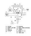
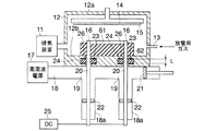
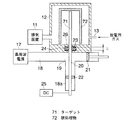
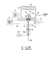
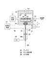
12 真空容器
13 放電用ガス導入機構
14 基板ホルダ
15 被処理基板
16 アンテナ
17 高周波電源
18 矩形導波管
19 導波管・同軸型伝送路変換器
20 内部導体
21 導波管プランジャ
22 導波管プランジャ
23 同軸型共振器
Claims (11)
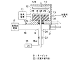
- 排気機構およびガス導入機構を有する真空容器の内部に設けられるアンテナと、このアンテナに電磁波伝送路を介して電磁波を供給する高周波電源とを備え、前記ガス導入機構により前記真空容器の内部に供給されたガスを前記アンテナに供給された前記電磁波による電力により電離してプラズマを生成し、このプラズマによって基板を処理するプラズマ処理装置において、
前記アンテナは、前記真空容器の壁部を貫通して設けられた同軸型伝送路の内部導体を延長して前記真空容器内に突出させた部分として構成され、かつ前記基板に対して垂直な位置関係で配置され、
前記同軸型伝送路における前記アンテナと反対側の端部には同軸型の可動式完全反射終端が設けられ、
前記電磁波は、前記真空容器と前記可動式完全反射終端との間に設置された変換器に供給され、そして、
前記アンテナに対してバイアス電圧を与える電源を備える、
ことを特徴とするプラズマ処理装置。 - 前記基板の処理はスパッタ成膜処理であり、前記アンテナはターゲットとして兼用されることを特徴とする請求項1記載のプラズマ処理装置。
- 前記同軸型伝送路が同一の前記電磁波伝送路に複数個設置され、かつ、前記複数個の同軸型伝送路のそれぞれの内部導体の一部が前記アンテナとして動作することを特徴とする請求項1または2記載のプラズマ処理装置。
- 前記複数個の同軸型伝送路で、前記真空容器の内部に位置するアンテナがターゲット部材で電気的に接続されていることを特徴とする請求項3記載のプラズマ処理装置。
- 前記アンテナはロッド状形態を有することを特徴とする請求項1〜4のいずれか1項に記載のプラズマ処理装置。
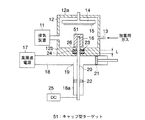
- 前記アンテナは端部に、前記基板に平行な板状ターゲット部を備えることを特徴とする請求項1〜3のいずれか1項に記載のプラズマ処理装置。
- ターゲットとして機能する部分の少なくとも下側領域に誘電体が設けられることを特徴とする請求項4または6記載のプラズマ処理装置。
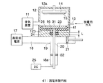
- 前記内部導体および前記アンテナにその軸方向に貫通したガス流路を形成し、前記真空容器の内部空間への放電用ガスの供給に用いることを特徴とする請求項1記載のプラズマ処理装置。
- 前記真空容器の壁部における前記内部導体の貫通部での前記アンテナと前記同軸型伝送路の間には同軸型共振器が設けられることを特徴とする請求項1〜8のいずれか1項に記載のプラズマ処理装置。
- バイアス電圧を与える前記電源は、前記アンテナの材料に応じて直流電源または高周波電源であることを特徴とする請求項1記載のプラズマ処理装置。
- 前記同軸型伝送路に供給される電磁波の周波数は2.45GHzであることを特徴とする請求項1記載のプラズマ処理装置。
Priority Applications (1)
| Application Number | Priority Date | Filing Date | Title |
|---|---|---|---|
| JP2003315481A JP4265762B2 (ja) | 2003-09-08 | 2003-09-08 | プラズマ処理装置 |
Applications Claiming Priority (1)
| Application Number | Priority Date | Filing Date | Title |
|---|---|---|---|
| JP2003315481A JP4265762B2 (ja) | 2003-09-08 | 2003-09-08 | プラズマ処理装置 |
Publications (2)
| Publication Number | Publication Date |
|---|---|
| JP2005082849A JP2005082849A (ja) | 2005-03-31 |
| JP4265762B2 true JP4265762B2 (ja) | 2009-05-20 |
Family
ID=34415739
Family Applications (1)
| Application Number | Title | Priority Date | Filing Date |
|---|---|---|---|
| JP2003315481A Expired - Fee Related JP4265762B2 (ja) | 2003-09-08 | 2003-09-08 | プラズマ処理装置 |
Country Status (1)
| Country | Link |
|---|---|
| JP (1) | JP4265762B2 (ja) |
Families Citing this family (13)
| Publication number | Priority date | Publication date | Assignee | Title |
|---|---|---|---|---|
| KR101064354B1 (ko) | 2006-11-09 | 2011-09-14 | 가부시키가이샤 알박 | 장벽막 형성 방법 |
| US8419854B2 (en) | 2007-04-17 | 2013-04-16 | Ulvac, Inc. | Film-forming apparatus |
| JP2009021220A (ja) * | 2007-06-11 | 2009-01-29 | Tokyo Electron Ltd | プラズマ処理装置、アンテナおよびプラズマ処理装置の使用方法 |
| JP2008305736A (ja) * | 2007-06-11 | 2008-12-18 | Tokyo Electron Ltd | プラズマ処理装置、プラズマ処理装置の使用方法およびプラズマ処理装置のクリーニング方法 |
| US8349156B2 (en) * | 2008-05-14 | 2013-01-08 | Applied Materials, Inc. | Microwave-assisted rotatable PVD |
| KR101730755B1 (ko) * | 2013-03-15 | 2017-04-26 | 도쿄엘렉트론가부시키가이샤 | 마이크로파 공진기 플라즈마 소스에서의 플라즈마 튜닝 로드 |
| JP2015193863A (ja) * | 2014-03-31 | 2015-11-05 | 株式会社Screenホールディングス | スパッタリング装置 |
| JP6167972B2 (ja) * | 2014-03-31 | 2017-07-26 | ブラザー工業株式会社 | 成膜装置 |
| WO2022009536A1 (ja) * | 2020-07-07 | 2022-01-13 | ソニーグループ株式会社 | スパッタリング装置およびスパッタリング成膜方法 |
| CN111826634B (zh) * | 2020-07-27 | 2023-03-31 | 中国科学院半导体研究所 | 一种高均一性半导体膜的生长装置及制备方法 |
| CN115346892A (zh) * | 2021-05-14 | 2022-11-15 | 日扬科技股份有限公司 | 固体结构的加工装置及加工方法 |
| KR20240051940A (ko) * | 2021-09-03 | 2024-04-22 | 도쿄엘렉트론가부시키가이샤 | 플라즈마 처리 장치 및 플라즈마 제어 방법 |
| JP7782870B2 (ja) * | 2024-04-11 | 2025-12-09 | 日本高周波株式会社 | プラズマ発生装置およびプラズマ発生方法 |
-
2003
- 2003-09-08 JP JP2003315481A patent/JP4265762B2/ja not_active Expired - Fee Related
Also Published As
| Publication number | Publication date |
|---|---|
| JP2005082849A (ja) | 2005-03-31 |
Similar Documents
| Publication | Publication Date | Title |
|---|---|---|
| JP5567005B2 (ja) | 回転可能なターゲットを備えたマイクロ波を援用したpvd | |
| US6899054B1 (en) | Device for hybrid plasma processing | |
| US5091049A (en) | High density plasma deposition and etching apparatus | |
| US4610770A (en) | Method and apparatus for sputtering | |
| JP4265762B2 (ja) | プラズマ処理装置 | |
| EP1976346A1 (en) | Apparatus for generating a plasma | |
| CN110382734B (zh) | 溅射装置 | |
| JPH0368773A (ja) | 高密度プラズマ蒸着およびエッチング装置 | |
| WO1990013909A1 (fr) | Installation de gravure a ions reactifs | |
| JP2002280196A (ja) | マイクロ波を利用したプラズマ発生装置 | |
| US20100078315A1 (en) | Microstrip antenna assisted ipvd | |
| US5234565A (en) | Microwave plasma source | |
| JP5582809B2 (ja) | プラズマ発生装置 | |
| JPH11135297A (ja) | プラズマ発生器 | |
| WO2020059273A1 (ja) | プラズマ処理方法およびプラズマ処理装置 | |
| JP3085021B2 (ja) | マイクロ波プラズマ処理装置 | |
| US9368313B1 (en) | Electronic amplifier device | |
| JP2000156374A (ja) | スパッタ処理応用のプラズマ処理装置 | |
| JP4384295B2 (ja) | プラズマ処理装置 | |
| RU2337426C1 (ru) | Релятивистский магнетрон с внешними каналами связи резонаторов | |
| RU2228560C1 (ru) | Релятивистский магнетрон | |
| JP2777657B2 (ja) | プラズマ付着装置 | |
| JPH0647723B2 (ja) | スパッタリング方法及びその装置 | |
| JPH08236448A (ja) | スパッタリング装置及びスパッタリング方法 | |
| JP3208995B2 (ja) | プラズマ処理方法及び装置 |
Legal Events
| Date | Code | Title | Description |
|---|---|---|---|
| A621 | Written request for application examination |
Free format text: JAPANESE INTERMEDIATE CODE: A621 Effective date: 20060825 |
|
| A977 | Report on retrieval |
Free format text: JAPANESE INTERMEDIATE CODE: A971007 Effective date: 20090129 |
|
| TRDD | Decision of grant or rejection written | ||
| A01 | Written decision to grant a patent or to grant a registration (utility model) |
Free format text: JAPANESE INTERMEDIATE CODE: A01 Effective date: 20090210 |
|
| A01 | Written decision to grant a patent or to grant a registration (utility model) |
Free format text: JAPANESE INTERMEDIATE CODE: A01 |
|
| A61 | First payment of annual fees (during grant procedure) |
Free format text: JAPANESE INTERMEDIATE CODE: A61 Effective date: 20090210 |
|
| R150 | Certificate of patent or registration of utility model |
Ref document number: 4265762 Country of ref document: JP Free format text: JAPANESE INTERMEDIATE CODE: R150 Free format text: JAPANESE INTERMEDIATE CODE: R150 |
|
| FPAY | Renewal fee payment (event date is renewal date of database) |
Free format text: PAYMENT UNTIL: 20120227 Year of fee payment: 3 |
|
| FPAY | Renewal fee payment (event date is renewal date of database) |
Free format text: PAYMENT UNTIL: 20130227 Year of fee payment: 4 |
|
| R250 | Receipt of annual fees |
Free format text: JAPANESE INTERMEDIATE CODE: R250 |
|
| R250 | Receipt of annual fees |
Free format text: JAPANESE INTERMEDIATE CODE: R250 |
|
| R250 | Receipt of annual fees |
Free format text: JAPANESE INTERMEDIATE CODE: R250 |
|
| R250 | Receipt of annual fees |
Free format text: JAPANESE INTERMEDIATE CODE: R250 |
|
| R250 | Receipt of annual fees |
Free format text: JAPANESE INTERMEDIATE CODE: R250 |
|
| R250 | Receipt of annual fees |
Free format text: JAPANESE INTERMEDIATE CODE: R250 |
|
| R250 | Receipt of annual fees |
Free format text: JAPANESE INTERMEDIATE CODE: R250 |
|
| R250 | Receipt of annual fees |
Free format text: JAPANESE INTERMEDIATE CODE: R250 |
|
| R250 | Receipt of annual fees |
Free format text: JAPANESE INTERMEDIATE CODE: R250 |
|
| R250 | Receipt of annual fees |
Free format text: JAPANESE INTERMEDIATE CODE: R250 |
|
| R250 | Receipt of annual fees |
Free format text: JAPANESE INTERMEDIATE CODE: R250 |
|
| LAPS | Cancellation because of no payment of annual fees |