JP4265762B2 - Plasma processing equipment - Google Patents
Plasma processing equipment Download PDFInfo
- Publication number
- JP4265762B2 JP4265762B2 JP2003315481A JP2003315481A JP4265762B2 JP 4265762 B2 JP4265762 B2 JP 4265762B2 JP 2003315481 A JP2003315481 A JP 2003315481A JP 2003315481 A JP2003315481 A JP 2003315481A JP 4265762 B2 JP4265762 B2 JP 4265762B2
- Authority
- JP
- Japan
- Prior art keywords
- antenna
- processing apparatus
- plasma processing
- plasma
- target
- Prior art date
- Legal status (The legal status is an assumption and is not a legal conclusion. Google has not performed a legal analysis and makes no representation as to the accuracy of the status listed.)
- Expired - Fee Related
Links
Images

Landscapes
- Physical Vapour Deposition (AREA)
- Chemical Vapour Deposition (AREA)
- Plasma Technology (AREA)
Description
本発明はプラズマ処理装置に関し、特に、マイクロ波領域等の電磁波の電力によってプラズマを生成し高密度プラズマの生成維持を可能とするプラズマ処理装置に関する。 The present invention relates to a plasma processing apparatus, and more particularly to a plasma processing apparatus that generates plasma with electric power of electromagnetic waves in a microwave region or the like and enables generation and maintenance of high-density plasma.
従来のスパッタ成膜装置は、高真空または超高真空に対応できる真空容器を用い、これに動作原理の異なる複数の真空ポンプを付設して真空容器内を高真空または超高真空の状態(分子流領域)になるように排気を行うことができるように構成されている。真空容器の内部には、成膜対象の基板を搭載する基板ホルダが設けられ、基板の成膜面に対向する位置関係でターゲットを配置してスパッタ成膜が行われる。このスパッタ成膜装置を用いて基板上に成膜を行うには、真空ポンプを作動させて真空容器内を高真空または超高真空の状態(分子流領域)まで排気し、その後に所定のガスを所定の圧力まで導入し、直流または高周波等の電力をターゲットに供給して真空容器内にプラズマを生成し、当該プラズマ中のイオンでターゲットをスパッタし、スパッタされたターゲット物質を基板に堆積させる。 A conventional sputter deposition apparatus uses a vacuum vessel that can handle high vacuum or ultra-high vacuum, and a plurality of vacuum pumps with different operating principles are attached to the vacuum vessel, and the inside of the vacuum vessel is in a high vacuum or ultra-high vacuum state (molecular The exhaust gas can be exhausted so as to be in the flow region. A substrate holder on which a substrate to be deposited is mounted is provided inside the vacuum container, and sputtering deposition is performed by placing a target in a positional relationship facing the deposition surface of the substrate. In order to form a film on a substrate using this sputter deposition apparatus, a vacuum pump is operated to evacuate the vacuum container to a high vacuum or ultrahigh vacuum state (molecular flow region), and then a predetermined gas To a predetermined pressure, DC or high frequency power is supplied to the target to generate plasma in the vacuum vessel, the target is sputtered with ions in the plasma, and the sputtered target material is deposited on the substrate. .
上記の一般的なスパッタ成膜装置に対して、従来、ガス流輸送型スパッタ成膜装置が提案されている(特許文献1、非特許文献1等)。ガス流輸送型スパッタ成膜装置では、スパッタ成膜時のガス圧力を比較的高く、かつガス流量を比較的大きく設定し、ガス流がいわゆる粘性流または中間流となる条件下で成膜を行うことを特徴としている。ガス流輸送型スパッタ成膜装置では、従来の一般的なスパッタ成膜装置のような分子流領域での排気を必要としないので、分子流領域で動作するターボ分子ポンプのような高価な真空ポンプを必要とせず、装置コストを安価なものに抑えることができる。なおガス流輸送型スパッタ成膜装置によれば、ガスによる基板冷却を行うことができるので、有機EL(エレクトロ・ルミネセンス)簿膜上やプラスチック等の材料を利用して作られた基板に対しても、特別な基板冷却機構を設けることなしにスパッタによる成膜を行うことができるという利点もある。 In contrast to the above general sputtering film forming apparatus, a gas flow transport type sputtering film forming apparatus has been proposed (Patent Document 1, Non-Patent Document 1, etc.). In the gas flow transport type sputtering film forming apparatus, the film pressure is set at a relatively high gas flow rate and the gas flow rate is set at a relatively large value so that the gas flow is a so-called viscous flow or intermediate flow. It is characterized by that. The gas flow transport type sputter film forming apparatus does not require exhaustion in the molecular flow region unlike the conventional general sputter film forming apparatus, so an expensive vacuum pump such as a turbo molecular pump operating in the molecular flow region. Therefore, the apparatus cost can be kept low. In addition, according to the gas flow transport type sputtering film forming apparatus, since the substrate can be cooled by the gas, the substrate made of a material such as an organic EL (electroluminescence) book film or plastic is used. However, there is also an advantage that film formation by sputtering can be performed without providing a special substrate cooling mechanism.
他方、上記の一般的なスパッタ成膜装置の改良型として、従来、イオン化スパッタ装置が提案されている。イオン化スパッタ装置では、装置構成は基本的には一般的なスパッタ装置と同一であるが、放電圧力を数10Pa程度と従来よりも高め、プラズマ生成のための電力源として高周波電力を用いて高密度のプラズマを生成する。この高密度プラズマを用いることによってターゲットからスパッタによって放出された金属原子をイオン化し、被処理基板上に垂直に入射させることで、従来のスパッタ装置では不可能であった高アスペクト比の穴の底部への成膜を可能としている。 On the other hand, an ionization sputtering apparatus has been proposed as an improved version of the above general sputtering film forming apparatus. In the ionization sputtering apparatus, the apparatus configuration is basically the same as that of a general sputtering apparatus, but the discharge pressure is increased to several tens Pa, which is higher than the conventional one, and high frequency power is used as a power source for plasma generation. The plasma is generated. By using this high-density plasma, the metal atoms released from the target by sputtering are ionized and vertically incident on the substrate to be processed, so that the bottom of the high-aspect-ratio hole that was impossible with conventional sputtering equipment It is possible to form a film.
上記の従来の一般的なスパッタ成膜装置では、成膜前に高真空または超高真空の状態への排気が必要とされ、さらに成膜中には分子流領域でのガス流制御が要求されるので、高真空または超高真空を実現する高価な真空ポンプが必要となり、装置コストが全体として非常に大きくなる。 In the conventional general sputtering film forming apparatus described above, evacuation to a high vacuum or ultra-high vacuum state is required before film formation, and further, gas flow control in the molecular flow region is required during film formation. Therefore, an expensive vacuum pump that realizes a high vacuum or an ultra-high vacuum is required, and the apparatus cost as a whole becomes very large.
プラズマを発生させるための電力として従来では直流電力または13.56MHzに代表される高周波電力を利用していた。通常の放電ではターゲットに対してこのような電力を供給しても、高密度プラズマを発生させることは困難であるため、ターゲットの裏面に設置した磁気回路を用いてターゲットの表面に磁場を発生させ、この磁場の作用でプラズマ密度を高めるいわゆるマグネトロンスパッタ装置が一般的に利用されていた。マグネトロンスパッタ装置においてはプラズマ密度として1×1011cm-3程度のプラズマ密度が得られ、従来のプロセスでは十分な成膜速度が得られていた。しかしながら、放電圧力を高くしてイオン化スパッタによる成膜を行う場合には、十分なプラズマ密度を得るには非常に大きな電力を必要とするという問題があった。 Conventionally, DC power or high-frequency power typified by 13.56 MHz has been used as power for generating plasma. In normal discharge, it is difficult to generate high-density plasma even if such power is supplied to the target. Therefore, a magnetic circuit installed on the back of the target is used to generate a magnetic field on the surface of the target. A so-called magnetron sputtering apparatus that increases the plasma density by the action of this magnetic field has been generally used. In the magnetron sputtering apparatus, a plasma density of about 1 × 10 11 cm −3 was obtained as a plasma density, and a sufficient film formation rate was obtained in the conventional process. However, when the film is formed by ionization sputtering at a high discharge pressure, there is a problem that very large electric power is required to obtain a sufficient plasma density.
一般に、放電圧力が数100Pa程度以下の圧力領域では、放電時の圧力を高くすると高密なプラズマの生成が容易になる。しかしながら、反面において、放電電圧も同時に低下するため、イオンの衝撃によるスパッタの効率は低くなり、結果的に堆積速度の低下をもたらすことになる。また圧力領域が数100Pa以上となると、一般的な放電手法を用いた場合には放電現象そのものが不安定となり、不均一かつ不連続的なアーク放電が発生するため、成膜装置としては成立しなくなる。さらに従来の上記の各スパッタ成膜装置において成膜装置内のガス圧力が高くなると、スパッタによってターゲットから放出された粒子は、成膜装置内のガス分子と頻繁に衝突するため基板まで到着する確率が低くなり、成膜速度の極端な低下を引き起こす。 In general, in a pressure region where the discharge pressure is about several hundred Pa or less, high-density plasma can be easily generated by increasing the pressure during discharge. However, on the other hand, since the discharge voltage also decreases at the same time, the sputtering efficiency due to ion bombardment is lowered, resulting in a decrease in the deposition rate. Also, when the pressure region is several hundred Pa or more, the discharge phenomenon itself becomes unstable when a general discharge method is used, and non-uniform and discontinuous arc discharge occurs. Disappear. Further, when the gas pressure in the film forming apparatus increases in each of the conventional sputter film forming apparatuses described above, the probability that particles emitted from the target by sputtering frequently collide with gas molecules in the film forming apparatus and thus reach the substrate. Lowers and causes an extreme decrease in the deposition rate.
なおた本出願に係る発明者等は、非特許文献2に基づいて、本発明に関連する技術の公表を行っている。非特許文献2に係る予稿集では、マイクロ波放電の有用性に基づき、アンテナをターゲットとし、かつこれに直流バイアスを供給するという構成に基づいてプラズマを成膜装置内に生じさせ、マイクロ波放電を用いたスパッタリング成膜の可能性と成膜結果を論じている。
本発明の課題は、ガス流輸送型スパッタ成膜装置等と同様に高真空または超高真空のための高価な真空ポンプが不要となり、全体としての装置コストが低く、放電圧力を高くしてスパッタリングによる成膜を行う場合において大きな電力を用いることなく十分なプラズマ密度を得ることができ、安定したアーク放電を得ることができ、成膜速度の高く保持できるようにするものである。 The object of the present invention is to eliminate the need for an expensive vacuum pump for high vacuum or ultra-high vacuum as in the gas flow transport type sputtering film forming apparatus, etc., and lower the overall apparatus cost and increase the discharge pressure for sputtering. In the case of forming a film by the above method, a sufficient plasma density can be obtained without using a large electric power, a stable arc discharge can be obtained, and the film forming speed can be kept high.
本発明の主な目的は、上記の課題に鑑み、マイクロ波等の領域の電磁波電力を利用して、従来と同程度または従来よりも高い動作圧力においてターゲット電極のごく近傍に効率良く高密度プラズマを生成することにより、基板上へ高速の成膜を行うことができるスパッタ成膜装置等のごときプラズマ処理装置を提供することにある。 In view of the above problems, the main object of the present invention is to use high-frequency plasma in the vicinity of the target electrode at the same or higher operating pressure than that of the prior art by using electromagnetic power in the microwave region. It is an object of the present invention to provide a plasma processing apparatus such as a sputter film forming apparatus that can form a film on a substrate at a high speed by generating.
本発明の他の目的は、動作圧力を高めることにより高真空または超高真空の排気装置を必要とせず、かつプラズマ生成効率を高めることにより放電用電源の小型化ができ、装置コストの低減も可能なプラズマ処理装置を提供することにある。 Another object of the present invention is that a high-vacuum or ultra-high vacuum exhaust device is not required by increasing the operating pressure, and the discharge power source can be reduced in size by increasing the plasma generation efficiency, thereby reducing the device cost. An object of the present invention is to provide a possible plasma processing apparatus.
本発明に係るプラズマ処理装置は、上記の目的を達成するために、次のように構成される。 In order to achieve the above object, a plasma processing apparatus according to the present invention is configured as follows.
第1のプラズマ処理装置(請求項1に対応):このプラズマ処理装置は、排気機構および放電用ガスのガス導入機構を有する真空容器の内部に設けられるアンテナと、このアンテナに導波管等の電磁波伝送路を介してマイクロ波領域等の電磁波を供給する高周波電源とを備える。ガス導入機構により真空容器の内部に供給された放電用ガスを上記のアンテナに供給された電磁波による電力により電離してプラズマを生成し、このプラズマによって真空容器内に置かれた基板を処理する。上記のアンテナは、真空容器の壁部を貫通して設けられた同軸型伝送路の内部導体を延長して真空容器内に突出させた部分として構成されると共に、基板に対して好ましくは垂直な位置関係となるように配置されている。同軸型伝送路におけるアンテナと反対側の端部には同軸型の可動式完全反射終端が設けられている。電磁波は、真空容器と可動式完全反射終端との間に設置された導波管・同軸型伝送路変換器に供給される。さらに上記のアンテナに対してはバイアス電圧を与える電源を備えている。 First plasma processing apparatus (corresponding to claim 1): This plasma processing apparatus includes an antenna provided inside a vacuum vessel having an exhaust mechanism and a gas introduction mechanism for a discharge gas, and a waveguide or the like provided in the antenna. A high-frequency power source that supplies electromagnetic waves in a microwave region or the like through an electromagnetic wave transmission path. The discharge gas supplied to the inside of the vacuum vessel by the gas introduction mechanism is ionized by the electric power generated by the electromagnetic wave supplied to the antenna to generate plasma, and the substrate placed in the vacuum vessel is processed by the plasma. The antenna is configured as a portion in which an inner conductor of a coaxial transmission line provided through the wall of the vacuum vessel is extended and protruded into the vacuum vessel, and is preferably perpendicular to the substrate. They are arranged in a positional relationship. A coaxial movable complete reflection terminal is provided at the end of the coaxial transmission line opposite to the antenna. The electromagnetic wave is supplied to a waveguide / coaxial transmission line converter installed between the vacuum vessel and the movable complete reflection terminal. Further, the antenna is provided with a power supply for applying a bias voltage.
上記のプラズマ処理装置では、成膜チャンバである真空容器内のガス圧力は代表的に5Pa程度に保持され、この状態で導波管等、および同軸型伝送路を通して高周波電源からアンテナにマイクロ波領域等の電磁波が供給される。高周波の電磁波電力によってアンテナ上に強い電界が発生させられる。これによって真空容器内に導入された放電用ガスが放電状態にされ、プラズマが生成される。 In the above plasma processing apparatus, the gas pressure in the vacuum chamber, which is the film forming chamber, is typically maintained at about 5 Pa, and in this state, the microwave region from the high-frequency power source to the antenna through the waveguide and the coaxial transmission line. Etc. are supplied. A strong electric field is generated on the antenna by the high frequency electromagnetic power. As a result, the discharge gas introduced into the vacuum vessel is discharged, and plasma is generated.
第2のプラズマ処理装置(請求項2に対応)は、上記の構成において、好ましくは、基板の処理はスパッタ成膜処理であり、アンテナはターゲットとして兼用されることで特徴づけられる。この構成によって、アンテナはプラズマ生成用のエネルギを供給する手段であると同時に、基板に堆積させる材料で作ることによりターゲットとして用いることも可能となる。 The second plasma processing apparatus (corresponding to claim 2) is characterized in that, in the above configuration, the processing of the substrate is a sputter film formation processing, and the antenna is also used as a target. With this configuration, the antenna is a means for supplying energy for generating plasma, and at the same time, it can be used as a target by being made of a material deposited on the substrate.
第3のプラズマ処理装置(請求項3に対応)は、上記の構成において、好ましくは、同軸型伝送路が同一の電磁波伝送路(単一の導波管型電磁波伝送路)に複数個設置され、かつ、複数個の同軸型伝送路のそれぞれの内部導体の一部が前述したアンテナとして動作することで特徴づけられる。真空容器内に設置されかつ処理される対象である基板の面積が大きい場合には、1つのアンテナでは、アンテナの径に制限があるために十分に基板の全面に均一な膜を十分に成膜することができない。そこで、例えば円板状の基板の面積の大きさに応じて所要数の複数のアンテナを設ける構造が望ましい。また上記の同軸型伝送路は、上記導波管型電磁波伝送路のE面の中心線上に配置されており、かつ、その間隔が概ね(2n−1)λg/2=2(λg:導波管内におけるマイクロ波の管内波長、n:1以上の整数)である。 In the third plasma processing apparatus (corresponding to claim 3), preferably, a plurality of coaxial transmission lines are installed in the same electromagnetic wave transmission line (single waveguide electromagnetic wave transmission line) in the above configuration. In addition, a part of the inner conductor of each of the plurality of coaxial transmission lines operates as the antenna described above. If the area of the substrate that is to be installed and processed in the vacuum vessel is large, one antenna has a sufficient uniform film over the entire surface of the substrate because the antenna diameter is limited. Can not do it. Therefore, for example, a structure in which a required number of antennas is provided in accordance with the size of the area of the disk-shaped substrate is desirable. The coaxial transmission line is disposed on the center line of the E-plane of the waveguide-type electromagnetic wave transmission line, and the interval is approximately (2n-1) λg / 2 = 2 (λg: waveguide). In-tube wavelength of microwave in tube, n is an integer of 1 or more).
第4のプラズマ処理装置(請求項4に対応)は、上記の構成において、好ましくは、複数個の同軸型伝送路で、真空容器の内部に位置するアンテナがターゲット部材で電気的に接続されていることで特徴づけられる。電気的な接続の仕方は、棒状であっても円板状であってもよい。この構成では、高周波電源から供給される電磁波電力を複数のルートで供給することができるので、各伝送路の負担が軽減される。 In the fourth plasma processing apparatus (corresponding to claim 4), in the above configuration, preferably, a plurality of coaxial transmission lines are used, and an antenna positioned inside the vacuum vessel is electrically connected by a target member. It is characterized by being. The electrical connection method may be rod-shaped or disk-shaped. In this configuration, the electromagnetic wave power supplied from the high-frequency power source can be supplied through a plurality of routes, so that the burden on each transmission path is reduced.
第5のプラズマ処理装置(請求項5に対応)は、上記の構成において、好ましくは、アンテナはロッド状形態を有することで特徴づけられる。ロッド状のアンテナは基板の成膜面に対して好ましくは垂直になるような位置関係で設けられる。真空容器内で突出した状態で設けられるロッド形状のアンテナの長さは、用途に応じて任意に設定される。 A fifth plasma processing apparatus (corresponding to claim 5) is characterized in that, in the above-mentioned configuration, the antenna preferably has a rod-like form. The rod-shaped antenna is provided in a positional relationship that is preferably perpendicular to the film formation surface of the substrate. The length of the rod-shaped antenna provided in a protruding state in the vacuum vessel is arbitrarily set according to the application.
第6のプラズマ処理装置(請求項6に対応)は、上記の構成において、好ましくは、アンテナは端部に板状ターゲット部を備えることを特徴とする。アンテナの先端部分に例えば円板状のターゲット部を別途の構成で設けることが可能である。基板の面積が大きい場合には、基板の成膜面の全面の均一な成膜を可能にするためには円板状ターゲット部を設けることが好ましい。 In the sixth plasma processing apparatus (corresponding to claim 6), in the above configuration, the antenna preferably includes a plate-like target portion at an end portion. For example, a disc-shaped target portion can be provided in a separate configuration at the tip portion of the antenna. When the area of the substrate is large, it is preferable to provide a disk-like target portion in order to allow uniform film formation on the entire film formation surface of the substrate.
第7のプラズマ処理装置(請求項7に対応)は、上記の構成において、好ましくは、ターゲットとして機能する部分の少なくとも下側領域に誘電体が設けられることで特徴づけられる。複数のアンテナを電気的に接続する場合、あるいは円板状ターゲット部をアンテナ先端部に備える場合には、その周囲の特定箇所で効率的にプラズマを生成することが要求される。そこで、望ましくない箇所でのプラズマ発生を抑制するために上記誘電体が当該箇所に配置される。 A seventh plasma processing apparatus (corresponding to claim 7) is characterized in that, in the above configuration, a dielectric is preferably provided in at least a lower region of a portion functioning as a target. When a plurality of antennas are electrically connected, or when a disk-shaped target portion is provided at the tip of the antenna, it is required to efficiently generate plasma at specific locations around the antenna. Therefore, in order to suppress plasma generation at an undesired location, the dielectric is disposed at the location.
第8のプラズマ処理装置(請求項8に対応)は、上記の構成において、好ましくは、内部導体とアンテナにその軸方向に貫通したガス流路を形成し、真空容器の内部空間への放電用ガスの供給に用いることで特徴づけられる。放電ガス圧力は広い範囲にわたることが望ましく、かつガス流が粘性流になることを想定すると、基板に向かって直接的に放電用ガスを吹き付けるような構成をさらに備えることが望ましい。 In the above configuration, the eighth plasma processing apparatus (corresponding to claim 8) preferably forms a gas flow path penetrating in the axial direction through the inner conductor and the antenna, and is used for discharging into the inner space of the vacuum vessel. It is characterized by being used for gas supply. It is desirable that the discharge gas pressure be in a wide range, and assuming that the gas flow becomes a viscous flow, it is desirable to further include a configuration in which the discharge gas is blown directly toward the substrate.
第9のプラズマ処理装置(請求項9に対応)は、上記の構成において、好ましくは、真空容器の壁部における内部導体の貫通部でのアンテナと上記の同軸型伝送路の間には同軸型共振器が設けられることを特徴とする。この構成によってアンテナには、高周波電源から供給された高周波電力に基づいて強い電界強度を生じさせることができる。 In the ninth plasma processing apparatus (corresponding to claim 9), in the above configuration, preferably, a coaxial type is provided between the antenna and the coaxial transmission line in the through portion of the inner conductor in the wall portion of the vacuum vessel. A resonator is provided. With this configuration, a strong electric field strength can be generated in the antenna based on the high frequency power supplied from the high frequency power source.
第10のプラズマ処理装置(請求項10に対応)は、上記の構成において、好ましくは、バイアス電圧を与える電源は、アンテナの材料に応じて直流電源または高周波電源であることで特徴づけられる。アンテナにバイアス電圧を与える電源は、ターゲットとしてのアンテナの材料に応じて決められる。アンテナが金属等の導電性物質である場合には直流電源であり、アンテナが誘電体であるときには高周波電源である。 The tenth plasma processing apparatus (corresponding to claim 10) is characterized in that, in the above configuration, the power supply for applying the bias voltage is a direct current power supply or a high frequency power supply depending on the material of the antenna. The power source for applying a bias voltage to the antenna is determined according to the material of the antenna as a target. When the antenna is a conductive material such as metal, it is a direct current power source, and when the antenna is a dielectric, it is a high frequency power source.
第11のプラズマ処理装置(請求項11に対応)は、上記の構成において、好ましくは、同軸型伝送路に供給される電磁波の周波数は2.45GHzであることを特徴とする。 In the eleventh plasma processing apparatus (corresponding to claim 11), in the above configuration, the frequency of the electromagnetic wave supplied to the coaxial transmission line is preferably 2.45 GHz.
本発明によれば、真空容器内に設置したアンテナにマイクロ波等の電磁波の電力を供給し、放電開始が容易で、かつ電力利用効率に優れたプラズマ生成を実現し、スパッタ成膜を初めとするプラズマを利用した種々の表面処理を簡便かつ安価な装置で可能にするという主たる効果が発揮される。 According to the present invention, power of electromagnetic waves such as microwaves is supplied to an antenna installed in a vacuum vessel, plasma generation that is easy to start discharge and excellent in power utilization efficiency is achieved, The main effect of enabling various surface treatments using plasma to be performed with a simple and inexpensive apparatus is exhibited.
以下に、本発明の好適な実施形態(実施例)を添付図面に基づいて説明する。 DESCRIPTION OF EMBODIMENTS Preferred embodiments (examples) of the present invention will be described below with reference to the accompanying drawings.
本発明に係るプラズマ処理装置の利用目的としては、一般的に、スパッタ成膜装置、プラズマCVD装置、ドライエッチング装置、表面処理装置等を想定している。以下の実施形態の説明では具体的な利用目的としてスパッタ成膜装置を対象とする。しかし、本発明の特徴的構成は、比較的高いプロセス圧力において動作可能である低コストプラズマプロセス装置に適用され、応用目的はこの実施形態に限定されるものではない。 In general, a plasma deposition apparatus, a plasma CVD apparatus, a dry etching apparatus, a surface treatment apparatus, and the like are assumed as usage purposes of the plasma processing apparatus according to the present invention. In the following description of the embodiment, a sputter deposition apparatus is targeted as a specific purpose of use. However, the characteristic configuration of the present invention is applied to a low-cost plasma process apparatus that can operate at a relatively high process pressure, and the application purpose is not limited to this embodiment.
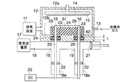
図1は本発明の第1実施形態に係るスパッタ成膜装置の概略的構成を示す。図1に示すスパッタ成膜装置は、排気装置11を備えた放電用真空容器12と、真空容器12内に導入する放電用ガス導入機構13と、真空容器12内の例えば天井部12aに配置される基板ホルダ14とを備えている。また基板ホルダ14には被処理基板15が固定状態で取り付けられている。真空容器12の図1中の下方壁部12bにはプラズマ生成用のアンテナ16が設置されている。アンテナ16を成す部材は全体として長形ロッド状であり、アンテナ16の先端部分は基板15に向かう方向に延びる状態で配置され、突出部分として形成されている。本実施形態では、アンテナ16の材質を被処理基板15上に堆積させる薄膜の材質と同じものとしている。これによってアンテナ16に成膜用ターゲットとしての機能も持たせている。
FIG. 1 shows a schematic configuration of a sputter deposition apparatus according to the first embodiment of the present invention. The sputter film forming apparatus shown in FIG. 1 is disposed on a
さらに図1では、アンテナ16に成膜用ターゲットとしての機能を持たせている。この場合において、アンテナとしての機能を逸脱しない限り、真空容器12の内部空間に突出した部分のみを基板15上に成膜される薄膜の材質と同じものにすることができる。
Further, in FIG. 1, the
高周波電力供給装置は、マイクロ波領域等(通常、300MHz〜30GHz)の高周波を出力する高周波電源17、当該高周波を伝送する矩形導波管18、導波管・同軸型伝送路変換器19、矩形導波管18にほぼ直交する位置関係にある長形の同軸型伝送路(内部導体20とその周囲の外部導体から成る)から構成されている。矩形導波管18の図1中の右側端末部には導波管プランジャ21が配置されている。導波管プランジャ21は、図示しない外部駆動装置によってその位置が適切に移動・調整される。上記同軸型伝送路は、上記の内部導体20とその周囲外側に位置する外部導体の部分(下記の円形導波管部18a)とによって構成される。内部導体20における図1中の上側端部の部分は、上記のごとくアンテナ16となっている。内部導体20におけるアンテナ16と反対側の部分に対応する円形導波管部18aには他の同軸プランジャ22が設けられている。内部導体20は、真空容器12の壁部12bを貫通するように配置されている。真空容器12の壁部12bの貫通部分で、アンテナ16と内部導体20の間には同軸型共振器23が設けられる。同軸型共振器23の内部には誘電体24が充填されている。またプラズマ生成用のアンテナ16には、内部導体20の下端部を介して、バイアス電圧を与えるための直流電源(DC)25が接続されている。
The high frequency power supply apparatus includes a high
次に上記構成を有するスパッタ成膜装置を動作させる手順を示す。 Next, a procedure for operating the sputter film forming apparatus having the above configuration will be described.
図1に示すスパッタ成膜装置を動作させるには、排気装置11を動作させて真空容器12の内部を10-3Pa程度まで排気し、放電用ガス導入機構13によって放電用ガスを導入する。真空容器12内のガス圧力は、放電用ガスの導入流量と排気装置11の排気速度により定まる。本実施形態に係るスパッタ成膜装置における典型的なガス圧力は5Pa程度である。所定のガス流量において所定の放電圧力を維持するために、排気装置11に排気速度を制御する機構を設けることは一般的に行われている。
In order to operate the sputter deposition apparatus shown in FIG. 1, the
次に本実施形態に係るスパッタ成膜装置におけるプラズマ生成機構に関して説明する。高周波電源17から発生した高周波電力(マイクロ波電力等)は、高周波電源17に内蔵される整合器によってインピーダンス整合を行った後に、矩形導波管18の内部をTE10モードで伝搬し、導波管・同軸型伝送路変換器19によってTEMモードに変換され、内部導体20を経てプラズマ生成用アンテナ16に供給される。
Next, the plasma generation mechanism in the sputter deposition apparatus according to this embodiment will be described. The high frequency power ( such as microwave power) generated from the high
矩形導波管18、導波管・同軸型伝送路変換器19からアンテナ16に至る内部導体20との間のインピーダンス整合は、矩形導波管18の端部に設けた導波管プランジャ21と、導波管・同軸型伝送路変換器19を貫通する内部導体20のうちのアンテナ16に対して反対側位置にある端部に設けた同軸型プランジャ22の調整によって行われる。導波管プランジャ21の作用は、導波管・同軸型伝送路変換器19によって矩形導波管18内に発生する定在波の強度を最小にすることである。同軸型プランジャ22の作用は、内部導体20でのマイクロ波電力がアンテナ16の方向にのみ伝搬させるための終端作用を持つと共に、アンテナ16および同軸型共振器23を含む内部導体での定在波比を調節することによりアンテナ16上に強い電界を発生させることにある。
The impedance matching between the
なお本実施形態においては、アンテナ16に対して直流電源25から直流バイアス電圧を供給するように構成しているため、内部導体20と外部導体である円形導波管部18aとは絶縁を行う構造または機能を有している。応用目的によってはアンテナ16を接地電位にする場合もある。この場合には絶縁構造は必要とされない。
In the present embodiment, since the DC bias voltage is supplied from the
次に本実施形態に係るスパッタ成膜装置の動作手順を簡単に説明する。高周波電源17からアンテナ16に供給された高周波電力は、アンテナ16から真空容器12内に放射され、内部に導入された放電用ガスを電離させて放電を生じさせる。この放電によって真空容器12の内部にプラズマが生成される。このとき、アンテナバイアス用直流電源25によりアンテナ16に対して所要の電位を与えることにより、プラズマ中のイオンが電界によって加速され、アンテナ16に衝突してアンテナ表面の金属原子をスパッタする。このスパッタされた金属原子は、被処理基板15の表面に順次に堆積し、被処理基板15の表面に薄膜が堆積され、形成される。
Next, the operation procedure of the sputter deposition apparatus according to this embodiment will be briefly described. The high-frequency power supplied from the high-
なお通常の直流または高周波に基づく放電を利用したスパッタ成膜装置では、ターゲットの表面に強い直流電界が発生し、この電界でイオンが加速されるため、アンテナバイアス用直流電源25は必要としない。一方、本実施形態のようにマイクロ波を用いた放電では、ターゲットであるアンテナ16の表面に発生する直流電圧はプラズマ電位程度であり、アンテナ16をターゲットとしてスパッタするには不十分である。そこで、この実施形態の構成ではスパッタ成膜装置として用いるにはアンテナバイアス用の直流電源25が必須となる。
Note that in a sputtering film forming apparatus using a normal direct current or high frequency discharge, a strong direct current electric field is generated on the surface of the target and ions are accelerated by this electric field, so that the antenna bias direct
上記の構成は装置全体の構成を複雑にするようにも見えるが、次のような大きな効果を有している。 Although the above configuration seems to complicate the configuration of the entire apparatus, it has the following great effects.
従来型のスパッタ成膜装置では、ターゲットに対するイオンの加速電圧は放電電力、放電時のガス種と圧力、真空容器の形状等に依存しており、加速電圧のみを独立に制御することができなかった。本実施形態の構成によれば、アンテナバイアス用直流電源25を動作させない場合のイオン加速電圧は、放電条件によらず0〜20V程度に維持される。この電圧は、ターゲットでのスパッタリング作用が発生する閾値と同程度以下であり、このためターゲットは実質的にスパッタされない。従って本実施形態によれば、イオン加速電圧をプラズマ密度と独立に制御することにより、プラズマ密度を一定としたまま成膜速度を制御することができる、およびイオン加速電圧を固定したまま成膜速度を制御することができる、といったように、成膜条件を自由かつ精密に制御でき、様々な特性を有する薄膜の形成を同一の装置で行うことができる。
In the conventional sputter deposition system, the acceleration voltage of ions with respect to the target depends on the discharge power, the gas type and pressure at the time of discharge, the shape of the vacuum vessel, etc., and the acceleration voltage alone cannot be controlled independently. It was. According to the configuration of the present embodiment, the ion acceleration voltage when the antenna bias
さらに、この特徴的構成の応用として、プラズマCVD、表面処理等のプロセスに適用する際には、アンテナ16のスパッタリングをほぼ無視できるため、アンテナ材料の付着による被処理基板15の表面の汚染を防ぐことができる。
Furthermore, as an application of this characteristic configuration, when applied to processes such as plasma CVD and surface treatment, the sputtering of the
またスパッタ成膜を行う前に、被処理基板15の表面をプラズマ処理して原子層レベルの汚染を除去する必要が生ずる場合がある。従来は、この前処理と成膜を別の真空容器を用いて行っていた。本実施形態の構成を適用すれば、最初にアンテナバイアス直流電源25を動作させずに基板15の表面処理を行い、次に、アンテナバイアス用直流電源25を動作させてスパッタ成膜を行うことが可能となる。従って、従来では2個必要とされた真空容器を1個に減らすことができ、装置の簡便化、低価格化に大きな効果がある。
In addition, it may be necessary to remove the contamination at the atomic layer level by performing plasma treatment on the surface of the substrate to be processed 15 before performing the sputter film formation. Conventionally, this pretreatment and film formation have been performed using separate vacuum vessels. If the configuration of this embodiment is applied, the surface treatment of the
また、図1に示すスパッタ成膜装置におけるプラズマ生成機構において特徴的である点は、導波管・同軸型伝送路変換器19とアンテナ16の間に設けられた同軸型共振器23である。同軸型共振器23の軸方向の長さ“L”は、供給されるマイクロ波の管内波長(λg)の1/2以上であることが望ましい。しかし、外部導体の内径が管内波長(λg)の1/2以上である場合にはこの限りではない。
Further, the plasma generation mechanism in the sputter deposition apparatus shown in FIG. 1 is characterized by a
導波管・同軸型伝送路変換器19から同軸型共振器23に伝搬したマイクロ波は同軸型共振器23内にTEMモードの定在波を生成し、その結果、同軸型共振器23内の電流密度が大きくなる。同軸型共振器23内で電流最大となる点は、同軸型共振器23とアンテナ16の境界部26であり、境界部26からアンテナ16の表面に流れ出す電流によりアンテナ16の表面に強い電界が発生する。
The microwave propagated from the waveguide / coaxial
真空容器12内にプラズマが生成されていない状況から放電を発生させるためには、アンテナ16の表面に強い電界が必要である。特に、ガス圧力が10Pa程度以上の場合には、放電開始に際して特に強い電界が必要となり、通常の方法でマイクロ波を供給するのみでは放電を発生させることは不可能であり、プラズマの生成のために強い電界、すなわち大きい電力が必要となる。
A strong electric field is required on the surface of the
放電開始以前にアンテナ16に大きい電力を供給することは、マイクロ波伝送経路における電力損失による発熱、伝送経路内の強い電界による絶縁破壊とアーク放電の発生、プラズマ発生直後に必要以上の高密度プラズマが生成されることによる装置へのダメージ等、多くの問題点がある。従って、必要最小限の電力で放電を開始できることが、実用的なプラズマプロセス装置にとって重要である。
Supplying large power to the
本実施形態による構成によれば、放電を開始させるための強い電界を生成するための問題点を、簡単な構造の同軸型共振器23を設けることによって解決している。これによって、小型かつ小電力の電源を用いた場合においても、安定してプラズマを生成することができる。
According to the configuration of the present embodiment, the problem for generating a strong electric field for starting discharge is solved by providing the
次に、第1実施形態に示した装置の概略の大きさを説明する。本実施形態の装置は、高周波電源の周波数として工業用周波数として指定されている2.45GHzの利用を想定して設計されている。従って、本実施形体に用いた矩形導波管18は2.45GHz用に設計されたものであり、代表的な寸法としては、E面幅100mm、H面幅50mmである。この矩形導波管18に装着する導波管・同軸型伝送路変換器19の内軸(内部導体20)の直径は、10mm程度であり、アンテナ16すなわちターゲットの直径もこれに従って10mm程度となる。本実施形態においては、同軸型共振器23の軸方向の長さLは20mmとしている。マイクロ波の波長は2.45GHzにおいては約12.2cmであるが、本実施形態における同軸共振器23は、内部に誘電体24としてアルミナ(比誘電率約9)が充填されているため、同軸型共振器23内の波長は約4cmとなる。この値は、前述したλgの1/2とほぼ等しいため、所要の強い電界強度を得るための共振器として動作する。
Next, the approximate size of the apparatus shown in the first embodiment will be described. The apparatus of this embodiment is designed on the assumption that the frequency of the high frequency power supply is 2.45 GHz, which is designated as an industrial frequency. Therefore, the
次に、本実施形態に示す装置をスパッタリング装置として動作させることによって得られる成膜プロセス上の特徴について述べる。本実施形態におけるアンテナ16はその直径がたかだか10mm程度であり、均一性よく成膜できる範囲は、動作圧力およびターゲット・基板間距離にも依存するが、アンテナ直径の数倍程度が限界である。しかしながら、本実施形態を適用した成膜プロセスにおいては、動作圧力を広い範囲で変化させることにより様々な特徴を持った薄膜を形成することができる。
Next, characteristics of the film forming process obtained by operating the apparatus shown in this embodiment as a sputtering apparatus will be described. The
本実施形態においては、アンテナ16の近くのプラズマ密度としては1012cm-3を得ることができ、アンテナ16に直流バイアスをかけることにより、アンテナ16の表面に入射するイオンの電流密度は、従来の平板マグネトロン放電の10倍程度に相当する100mA/cm-3を得ることができる。従って、アンテナ16の材質を成膜したい材料と同一にしてスパッタ用ターゲットとして用いることにより、高密度プラズマによる高イオン電流密度を利用したスパッタ成膜が可能となり、従来と異なる特徴を持つ薄膜を生成することができる。
In the present embodiment, 10 12 cm −3 can be obtained as the plasma density near the
例えば、アンテナ16の材質として金を用いた場合には、放電圧力を5Pa程度以下にすることで金薄膜の高速成膜が可能である。
For example, when gold is used as the material of the
また放電圧力を数10Paとすることにより、スパッタされた金原子がプラズマ中で高い確率でイオン化されるため、基板表面に形成された微細な孔、溝等の構造部の底部への成膜が可能となる。このような成膜手法は、イオン化スパッタ成膜技術として知られているが、従来は大電力の高周波マグネトロン放電または直流マグネトロン放電と高周波放電の組み合わせによる大がかりな装置を必要としている。本実施形態の装置をこのような成膜プロセスに適用することによって、従来よりも簡便かつ安価な装置によって、同等の成膜性能を得ることができる。 Also, by setting the discharge pressure to several tens of Pa, the sputtered gold atoms are ionized with high probability in the plasma, so that the film is formed on the bottom of the structure portion such as fine holes and grooves formed on the substrate surface. It becomes possible. Such a film forming technique is known as an ionized sputtering film forming technique, but conventionally, a large-scale apparatus using a high-power high-frequency magnetron discharge or a combination of a direct-current magnetron discharge and a high-frequency discharge is required. By applying the apparatus of the present embodiment to such a film forming process, the same film forming performance can be obtained with an apparatus that is simpler and less expensive than the conventional apparatus.
放電圧力をさらに高い数100Pa以上の領域とすると、スパッタされた金原子は微粒子となって基板に付着する。数100Pa程度の圧力においては、金原子は気相中での微粒子としての成長速度は遅く、基板に付着した後に、直径数10mm程度の微粒子状の構造を持った薄膜として成長する。さらに高い圧力においては、金原子は気相中で直径数100mm程度の微粒子に成長して基板に付着する。 When the discharge pressure is set to a higher region of several hundred Pa or more, the sputtered gold atoms become fine particles and adhere to the substrate. At a pressure of about several hundred Pa, the growth rate of gold atoms as fine particles in the gas phase is slow, and after growing on the substrate, it grows as a thin film having a fine particle structure with a diameter of about several tens of millimeters. At a higher pressure, gold atoms grow into fine particles having a diameter of about several hundred mm in the gas phase and adhere to the substrate.
上記のような微粒子または微粒子状の薄膜は、様々な波長の光を吸収するセンサ素子、大きな実効表面積による触媒作用の利用等の応用が期待されている。 The fine particles or fine particle-like thin films as described above are expected to be applied to sensor elements that absorb light of various wavelengths and use of catalytic action due to a large effective surface area.
また、本実施形態に係る装置と従来装置との大きな違いとして、従来装置ではプラズマを発生し維持するための外部磁場が必要なことが挙げられる。磁性薄膜を形成する際には、ターゲット材料として鉄、コバルト等の強磁性体を用いるが、従来のマグネトロン放電装置ではターゲットの裏面に磁石を設置するため、磁場がターゲットによって遮蔽されてしまい、プラズマ生成効率が低下する。従来は、この欠点を補うため強力な磁石を用いるが、この場合にも磁場がターゲットの表面近くに集中するため、ターゲットの利用効率が低下するという問題点があった。さらに強力な磁石をターゲット裏面に組み込む作業は、技術的な困難を伴ない、作業ミスによる事故発生の危険性も大きかった。 A significant difference between the apparatus according to the present embodiment and the conventional apparatus is that the conventional apparatus requires an external magnetic field for generating and maintaining plasma. When forming a magnetic thin film, a ferromagnetic material such as iron or cobalt is used as a target material. However, in a conventional magnetron discharge device, a magnet is placed on the back surface of the target, so that the magnetic field is shielded by the target and plasma Production efficiency decreases. Conventionally, a strong magnet is used to compensate for this drawback. However, in this case as well, there is a problem that the use efficiency of the target is lowered because the magnetic field is concentrated near the surface of the target. In addition, the work of incorporating a powerful magnet on the back of the target was accompanied by technical difficulties and a large risk of accidents due to work mistakes.
上記に対して、本実施形態の特徴的構成は、強磁性体ターゲットを用いたスパッタ成膜装置に用いることにより、上記の問題点を解決した磁性薄膜形成装置として用いることができる。 On the other hand, the characteristic configuration of the present embodiment can be used as a magnetic thin film forming apparatus that solves the above problems by using it in a sputter film forming apparatus using a ferromagnetic target.
次に図2を参照して本発明の第2実施形態を説明する。図2において、図1に説明した要素と実質的に同一の要素には同一の符合を付している。第1実施形態に係る装置をスパッタリングによる成膜に応用する場合には、前述したようにアンテナ16の外径が制限されるため、被処理基板15の面積にも制約があり、大面積の基板に成膜することには不適切であった。
Next, a second embodiment of the present invention will be described with reference to FIG. In FIG. 2, elements that are substantially the same as those described in FIG. When the apparatus according to the first embodiment is applied to film formation by sputtering, since the outer diameter of the
この第2実施形態では、全体装置としての構成は基本的に同じであり、さらにこの構成において、第1実施形態で説明したアンテナ16に関する部分と同じ構造の、ターゲットとしての機能を有するアンテナを複数本、例えば3本設置している。成膜速度分布はそれぞれのターゲット単独の場合の重ね合わせとなるため、より大面積の被処理基板15に対して均一性良く成膜することができる。その他の構成は第1実施形態と同じである。
In the second embodiment, the configuration as the entire apparatus is basically the same, and in this configuration, a plurality of antennas having the same structure as the portion related to the
それぞれのアンテナ16は、矩形導波管18の長さ方向に、一定の間隔を置いて設置されている。この構造によって、すべてのアンテナ16をプラズマ生成のために動作させることができる。また、3つのアンテナ16に対する電磁波の供給電力に偏りが出る場合には、導波管プランジャ21の位置を調整することによって修正することができる。
The
第2実施形態によれば、長方形の大面積の基板15に対し均一性の良好な成膜を行うことができる。また成膜中に基板15を移動させることよって走査動作を行わせ、より大面積の矩形基板または円形基板に対する成膜も可能である。
According to the second embodiment, film formation with good uniformity can be performed on a rectangular large-
次に図3を参照して本発明の第3実施形態を説明する。図3において、図1に説明した要素と実質的に同一の要素には同一の符合を付している。この実施形態では、アンテナ16の終端に円板型のターゲット31を別要素としてまたは一体的に設けるようにしている。さらにターゲット31の裏面側に、放電を抑制しかつターゲット31の表面側領域および側面側領域に効率的にプラズマを生成するための誘電体製の円板32を装着した。円板32と、アンテナ16、ターゲット31、真空容器11の内壁面のそれぞれとの接触部は密接させられる。その他の構成は第1実施形態と同じである。
Next, a third embodiment of the present invention will be described with reference to FIG. 3, elements that are substantially the same as the elements described in FIG. In this embodiment, a disc-shaped
第3実施形態によれば、ターゲット31の裏面でのプラズマ生成を抑制することによって電力の利用効率を向上させ、ターゲット31の表面および側面のみに、効率良く高密度なプラズマを生成することができる。その結果、円形の大面積基板15に対して均一性の良好な成膜を行うことが可能になると同時に、基板15の表面以外の部分への堆積物の付着量を減量することができ、ターゲット利用効率の向上が望める。
According to the third embodiment, power generation efficiency can be improved by suppressing plasma generation on the back surface of the
次に図4を参照して本発明の第4実施形態を説明する。第4実施形態は第3実施形態の変形例である。この実施形態においては、アンテナ16の終端に円板型のターゲット31を設けると共に、さらにターゲット31の裏面および側面での放電を抑制してターゲット31の表面に効率的にプラズマを生成するための誘電体製の円板41を装着した。本実施形態によれば、円形の大面積基板15に対し均一性の良好な製膜が可能となる。
Next, a fourth embodiment of the present invention will be described with reference to FIG. The fourth embodiment is a modification of the third embodiment. In this embodiment, a disc-shaped
上記の第3実施形態との違いは、ターゲット31の側面のスパッタリングの有無に関するもののみである。ターゲット31の側面のスパッタリングは、被処理基板15上の成膜速度分布に影響があるため、使用目的に応じて第3実施形態または第4実施形態を選択して使用することができる。
The difference from the third embodiment described above is only related to the presence or absence of sputtering on the side surface of the
図5を参照して本発明の第5実施形態を説明する。この実施形態においてはアンテナ16の終端にキャップ型のターゲット51を装着した。ターゲット51とアンテナ16とは密着させて設置することが望ましい。その他の構成は、第1実施形態と同じである。
A fifth embodiment of the present invention will be described with reference to FIG. In this embodiment, a cap-
本実施形態によれば、プラズマ生成状況に影響を与えずに、ターゲット部分の交換を容易に行うことができる。なお、図5においてはターゲット51の外径をアンテナ16の外径よりも大きくした例を示しているが、アンテナ16の外径を小さくして、ターゲット51の外径を円柱ロッド状の内部導体20の外径と等しくすることも可能である。
According to the present embodiment, the target portion can be easily replaced without affecting the plasma generation state. 5 shows an example in which the outer diameter of the
またターゲット51の材質として誘電体を用いた場合にも、アンテナ16で伝搬される電磁波によってターゲット51の表面にプラズマを生成することが可能である。なお誘電体ターゲットのスパッタリングを行うには、バイアス電圧を与える電源として高周波電源が用いられる。
Even when a dielectric is used as the material of the
図6を参照して本発明の第6実施形態を説明する。本実施形態では、前述したアンテナ16が2箇所に設置され、当該2つのアンテナ16の先端が金属製のターゲット61で接続されている。ターゲット61は棒状であっても、円盤状であっても良い。またターゲット61のうち被処理基板15に対向しない面と真空容器11との間の空間には、第3実施形態または第4実施形態の場合と同様に、誘電体製のブロック62が設置されている。その他の構成は、第1実施形態と実質的に同じである。
A sixth embodiment of the present invention will be described with reference to FIG. In the present embodiment, the
本実施形態によれば、単一のターゲット61に対して2箇所から電磁波を供給することができ、同軸型伝送路に負担を与えずに大きな電力を供給することができ、成膜速度の向上が可能である。またターゲット61上のプラズマ密度分布は、導波管プランジャ21の位置の調整によって制御される。
According to the present embodiment, electromagnetic waves can be supplied from two locations to a
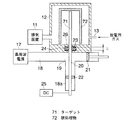
次に図7を参照して本発明の第7実施形態を説明する。本実施形態では、ターゲットであるロッド状の前述のアンテナ16に対して長形のターゲット71を設け、このターゲット71の周辺に、図7に示すように頂部に壁部を有する円筒形の被処理物72を配置するように構成される。これにより、被処理物72の内面に所定の材質の薄膜を形成することができる。ターゲット71の長さは、被処理物72の形状に合わせて自由に設定することができる。その他の構成については、第1実施形態の構成と同じである。
Next, a seventh embodiment of the present invention will be described with reference to FIG. In the present embodiment, a
上記の各実施形態は、本発明に係るプラズマ処理装置をスパッタ成膜装置に応用した例を示したが、次には、CVD、表面改質等の被処理基板の表面処理に応用した実施形態を示す。 Each of the above embodiments has shown an example in which the plasma processing apparatus according to the present invention is applied to a sputtering film forming apparatus. Next, an embodiment in which the plasma processing apparatus is applied to a surface treatment of a substrate to be processed such as CVD or surface modification. Indicates.
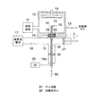
図8に本発明の第8の実施形態を示す。本実施形態においてはアンテナ16および内部導体20の軸方向に貫通したガス流路81を設け、このガス流路81を通して放電用ガス82の供給が行われるように構成している。その他の構成は、第1実施形態の構成と同じである。
FIG. 8 shows an eighth embodiment of the present invention. In the present embodiment, a
本発明で想定している放電用ガスの圧力は広い範囲にわたっているが、第8実施形態においては真空容器11内のガス流が粘性流となるような圧力領域を想定している。粘性流領域における被処理基板上のプロセス速度分布はガスの流れに強く影響される。本実施形態によれば、放電用ガスを被処理基板15に向かって吹き付けることができるので、真空容器11の内壁の形状または他の実施形態におけるガス導入機構13の位置が真空容器11内のガスの流れに対する影響を最小限にとどめることができ、より均一性に優れた表面処理が可能となる。
Although the pressure of the discharge gas assumed in the present invention covers a wide range, the eighth embodiment assumes a pressure region in which the gas flow in the
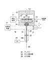
図9に本発明の第9の実施形態を示す。この実施形態は、第8実施形態の変形例である。円盤型のアンテナ91の内部にガス分散空間92を設け、複数個のガス流路93からガスを放出することによって、第8実施形態の特徴を生かしたまま、より大面積の被処理基板15に対して均一性に優れた表面処理を可能としている。
FIG. 9 shows a ninth embodiment of the present invention. This embodiment is a modification of the eighth embodiment. A
上記において、実施形態で説明された構成、形状、大きさおよび配置関係については本発明が理解・実施できる程度に概略的に示したものにすぎず、また数値および各構成要素の組成(材質)については例示にすぎない。従って本発明は上記実施形態に限定されるものではなく、特許請求の範囲に示される技術的思想の範囲を逸脱しない限り様々な形態に変更することができる。 In the above description, the configuration, shape, size, and arrangement relationship described in the embodiments are merely schematically shown to the extent that the present invention can be understood and implemented, and numerical values and compositions (materials) of each component. Is merely an example. Therefore, the present invention is not limited to the above-described embodiments, and various modifications can be made without departing from the scope of the technical idea shown in the claims.
本発明は、基板処理チャンバの内部に容器壁部を通してロッド形状等のアンテナを配置し、このアンテナにマイクロ波等に基づく高周波電力を供給してその周辺領域に強く電界強度を発生させることにより放電用ガスを電離してプラズマを生成し、相対的に高い圧力状態で基板処理を可能にする装置に利用される。 According to the present invention, a rod-shaped antenna is disposed inside a substrate processing chamber through a container wall, and a high-frequency electric power based on a microwave is supplied to the antenna to generate a strong electric field strength in the peripheral region. It is used in an apparatus that ionizes a working gas to generate plasma and enables substrate processing at a relatively high pressure.
11 排気装置
12 真空容器
13 放電用ガス導入機構
14 基板ホルダ
15 被処理基板
16 アンテナ
17 高周波電源
18 矩形導波管
19 導波管・同軸型伝送路変換器
20 内部導体
21 導波管プランジャ
22 導波管プランジャ
23 同軸型共振器
DESCRIPTION OF
Claims (11)
前記アンテナは、前記真空容器の壁部を貫通して設けられた同軸型伝送路の内部導体を延長して前記真空容器内に突出させた部分として構成され、かつ前記基板に対して垂直な位置関係で配置され、
前記同軸型伝送路における前記アンテナと反対側の端部には同軸型の可動式完全反射終端が設けられ、
前記電磁波は、前記真空容器と前記可動式完全反射終端との間に設置された変換器に供給され、そして、
前記アンテナに対してバイアス電圧を与える電源を備える、
ことを特徴とするプラズマ処理装置。 An antenna provided inside a vacuum vessel having an exhaust mechanism and a gas introduction mechanism, and a high-frequency power source for supplying electromagnetic waves to the antenna via an electromagnetic wave transmission path are supplied to the inside of the vacuum vessel by the gas introduction mechanism. In a plasma processing apparatus for generating a plasma by ionizing the generated gas by the electric power generated by the electromagnetic wave supplied to the antenna, and processing the substrate by the plasma,
The antenna is configured as a portion in which an inner conductor of a coaxial transmission line provided through the wall of the vacuum vessel is extended and protruded into the vacuum vessel, and is positioned perpendicular to the substrate Arranged in a relationship,
A coaxial movable complete reflection termination is provided at the end of the coaxial transmission line opposite to the antenna,
The electromagnetic wave is supplied to a transducer installed between the vacuum vessel and the movable fully reflective termination; and
A power supply for applying a bias voltage to the antenna;
A plasma processing apparatus.
Priority Applications (1)
| Application Number | Priority Date | Filing Date | Title |
|---|---|---|---|
| JP2003315481A JP4265762B2 (en) | 2003-09-08 | 2003-09-08 | Plasma processing equipment |
Applications Claiming Priority (1)
| Application Number | Priority Date | Filing Date | Title |
|---|---|---|---|
| JP2003315481A JP4265762B2 (en) | 2003-09-08 | 2003-09-08 | Plasma processing equipment |
Publications (2)
| Publication Number | Publication Date |
|---|---|
| JP2005082849A JP2005082849A (en) | 2005-03-31 |
| JP4265762B2 true JP4265762B2 (en) | 2009-05-20 |
Family
ID=34415739
Family Applications (1)
| Application Number | Title | Priority Date | Filing Date |
|---|---|---|---|
| JP2003315481A Expired - Fee Related JP4265762B2 (en) | 2003-09-08 | 2003-09-08 | Plasma processing equipment |
Country Status (1)
| Country | Link |
|---|---|
| JP (1) | JP4265762B2 (en) |
Families Citing this family (13)
| Publication number | Priority date | Publication date | Assignee | Title |
|---|---|---|---|---|
| KR101064354B1 (en) | 2006-11-09 | 2011-09-14 | 가부시키가이샤 알박 | Barrier Film Formation Method |
| US8419854B2 (en) | 2007-04-17 | 2013-04-16 | Ulvac, Inc. | Film-forming apparatus |
| JP2009021220A (en) * | 2007-06-11 | 2009-01-29 | Tokyo Electron Ltd | Plasma processing apparatus, antenna, and method of using plasma processing apparatus |
| JP2008305736A (en) * | 2007-06-11 | 2008-12-18 | Tokyo Electron Ltd | Plasma processing apparatus, method of using plasma processing apparatus, and method of cleaning plasma processing apparatus |
| US8349156B2 (en) * | 2008-05-14 | 2013-01-08 | Applied Materials, Inc. | Microwave-assisted rotatable PVD |
| KR101730755B1 (en) * | 2013-03-15 | 2017-04-26 | 도쿄엘렉트론가부시키가이샤 | Plasma tuning rods in microwave resonator plasma sources |
| JP2015193863A (en) * | 2014-03-31 | 2015-11-05 | 株式会社Screenホールディングス | sputtering device |
| JP6167972B2 (en) * | 2014-03-31 | 2017-07-26 | ブラザー工業株式会社 | Deposition equipment |
| WO2022009536A1 (en) * | 2020-07-07 | 2022-01-13 | ソニーグループ株式会社 | Sputtering apparatus and sputtering film forming method |
| CN111826634B (en) * | 2020-07-27 | 2023-03-31 | 中国科学院半导体研究所 | Growth device and preparation method of high-uniformity semiconductor film |
| CN115346892A (en) * | 2021-05-14 | 2022-11-15 | 日扬科技股份有限公司 | Processing device and processing method for solid structure |
| KR20240051940A (en) * | 2021-09-03 | 2024-04-22 | 도쿄엘렉트론가부시키가이샤 | Plasma processing device and plasma control method |
| JP7782870B2 (en) * | 2024-04-11 | 2025-12-09 | 日本高周波株式会社 | Plasma generating device and plasma generating method |
-
2003
- 2003-09-08 JP JP2003315481A patent/JP4265762B2/en not_active Expired - Fee Related
Also Published As
| Publication number | Publication date |
|---|---|
| JP2005082849A (en) | 2005-03-31 |
Similar Documents
| Publication | Publication Date | Title |
|---|---|---|
| JP5567005B2 (en) | Microwave-assisted PVD with a rotatable target | |
| US6899054B1 (en) | Device for hybrid plasma processing | |
| US5091049A (en) | High density plasma deposition and etching apparatus | |
| US4610770A (en) | Method and apparatus for sputtering | |
| JP4265762B2 (en) | Plasma processing equipment | |
| EP1976346A1 (en) | Apparatus for generating a plasma | |
| CN110382734B (en) | Sputtering device | |
| JPH0368773A (en) | Dense plasma vapor deposition and etching device | |
| WO1990013909A1 (en) | Reactive ion etching apparatus | |
| JP2002280196A (en) | Plasma generating device using microwave | |
| US20100078315A1 (en) | Microstrip antenna assisted ipvd | |
| US5234565A (en) | Microwave plasma source | |
| JP5582809B2 (en) | Plasma generator | |
| JPH11135297A (en) | Plasma generator | |
| WO2020059273A1 (en) | Plasma processing method and plasma processing apparatus | |
| JP3085021B2 (en) | Microwave plasma processing equipment | |
| US9368313B1 (en) | Electronic amplifier device | |
| JP2000156374A (en) | Plasma processing equipment for sputter processing | |
| JP4384295B2 (en) | Plasma processing equipment | |
| RU2337426C1 (en) | Relativistic magnetron with external channels of resonators communication | |
| RU2228560C1 (en) | Relativistic magnetron | |
| JP2777657B2 (en) | Plasma deposition equipment | |
| JPH0647723B2 (en) | Sputtering method and apparatus | |
| JPH08236448A (en) | Sputtering apparatus and sputtering method | |
| JP3208995B2 (en) | Plasma processing method and apparatus |
Legal Events
| Date | Code | Title | Description |
|---|---|---|---|
| A621 | Written request for application examination |
Free format text: JAPANESE INTERMEDIATE CODE: A621 Effective date: 20060825 |
|
| A977 | Report on retrieval |
Free format text: JAPANESE INTERMEDIATE CODE: A971007 Effective date: 20090129 |
|
| TRDD | Decision of grant or rejection written | ||
| A01 | Written decision to grant a patent or to grant a registration (utility model) |
Free format text: JAPANESE INTERMEDIATE CODE: A01 Effective date: 20090210 |
|
| A01 | Written decision to grant a patent or to grant a registration (utility model) |
Free format text: JAPANESE INTERMEDIATE CODE: A01 |
|
| A61 | First payment of annual fees (during grant procedure) |
Free format text: JAPANESE INTERMEDIATE CODE: A61 Effective date: 20090210 |
|
| R150 | Certificate of patent or registration of utility model |
Ref document number: 4265762 Country of ref document: JP Free format text: JAPANESE INTERMEDIATE CODE: R150 Free format text: JAPANESE INTERMEDIATE CODE: R150 |
|
| FPAY | Renewal fee payment (event date is renewal date of database) |
Free format text: PAYMENT UNTIL: 20120227 Year of fee payment: 3 |
|
| FPAY | Renewal fee payment (event date is renewal date of database) |
Free format text: PAYMENT UNTIL: 20130227 Year of fee payment: 4 |
|
| R250 | Receipt of annual fees |
Free format text: JAPANESE INTERMEDIATE CODE: R250 |
|
| R250 | Receipt of annual fees |
Free format text: JAPANESE INTERMEDIATE CODE: R250 |
|
| R250 | Receipt of annual fees |
Free format text: JAPANESE INTERMEDIATE CODE: R250 |
|
| R250 | Receipt of annual fees |
Free format text: JAPANESE INTERMEDIATE CODE: R250 |
|
| R250 | Receipt of annual fees |
Free format text: JAPANESE INTERMEDIATE CODE: R250 |
|
| R250 | Receipt of annual fees |
Free format text: JAPANESE INTERMEDIATE CODE: R250 |
|
| R250 | Receipt of annual fees |
Free format text: JAPANESE INTERMEDIATE CODE: R250 |
|
| R250 | Receipt of annual fees |
Free format text: JAPANESE INTERMEDIATE CODE: R250 |
|
| R250 | Receipt of annual fees |
Free format text: JAPANESE INTERMEDIATE CODE: R250 |
|
| R250 | Receipt of annual fees |
Free format text: JAPANESE INTERMEDIATE CODE: R250 |
|
| R250 | Receipt of annual fees |
Free format text: JAPANESE INTERMEDIATE CODE: R250 |
|
| LAPS | Cancellation because of no payment of annual fees |