JP4247282B2 - 圧電基板及びその製造方法 - Google Patents
圧電基板及びその製造方法 Download PDFInfo
- Publication number
- JP4247282B2 JP4247282B2 JP2007045045A JP2007045045A JP4247282B2 JP 4247282 B2 JP4247282 B2 JP 4247282B2 JP 2007045045 A JP2007045045 A JP 2007045045A JP 2007045045 A JP2007045045 A JP 2007045045A JP 4247282 B2 JP4247282 B2 JP 4247282B2
- Authority
- JP
- Japan
- Prior art keywords
- film
- piezoelectric substrate
- substrate
- main surface
- base material
- Prior art date
- Legal status (The legal status is an assumption and is not a legal conclusion. Google has not performed a legal analysis and makes no representation as to the accuracy of the status listed.)
- Active
Links
- 239000000758 substrate Substances 0.000 title claims description 124
- 238000004519 manufacturing process Methods 0.000 title claims description 13
- 239000000463 material Substances 0.000 claims description 55
- 238000000034 method Methods 0.000 claims description 19
- VYPSYNLAJGMNEJ-UHFFFAOYSA-N Silicium dioxide Chemical compound O=[Si]=O VYPSYNLAJGMNEJ-UHFFFAOYSA-N 0.000 claims description 10
- GQYHUHYESMUTHG-UHFFFAOYSA-N lithium niobate Chemical compound [Li+].[O-][Nb](=O)=O GQYHUHYESMUTHG-UHFFFAOYSA-N 0.000 claims description 9
- 239000002245 particle Substances 0.000 claims description 9
- 239000002002 slurry Substances 0.000 claims description 8
- 150000001875 compounds Chemical class 0.000 claims description 6
- 229910052710 silicon Inorganic materials 0.000 claims description 6
- XLOMVQKBTHCTTD-UHFFFAOYSA-N Zinc monoxide Chemical compound [Zn]=O XLOMVQKBTHCTTD-UHFFFAOYSA-N 0.000 claims description 5
- 238000000576 coating method Methods 0.000 claims description 5
- WSMQKESQZFQMFW-UHFFFAOYSA-N 5-methyl-pyrazole-3-carboxylic acid Chemical compound CC1=CC(C(O)=O)=NN1 WSMQKESQZFQMFW-UHFFFAOYSA-N 0.000 claims description 4
- 229910052751 metal Inorganic materials 0.000 claims description 4
- 239000002184 metal Substances 0.000 claims description 4
- 239000006104 solid solution Substances 0.000 claims description 4
- 229910052580 B4C Inorganic materials 0.000 claims description 3
- 229910052581 Si3N4 Inorganic materials 0.000 claims description 3
- GWEVSGVZZGPLCZ-UHFFFAOYSA-N Titan oxide Chemical compound O=[Ti]=O GWEVSGVZZGPLCZ-UHFFFAOYSA-N 0.000 claims description 3
- 229910045601 alloy Inorganic materials 0.000 claims description 3
- 239000000956 alloy Substances 0.000 claims description 3
- INAHAJYZKVIDIZ-UHFFFAOYSA-N boron carbide Chemical compound B12B3B4C32B41 INAHAJYZKVIDIZ-UHFFFAOYSA-N 0.000 claims description 3
- PMHQVHHXPFUNSP-UHFFFAOYSA-M copper(1+);methylsulfanylmethane;bromide Chemical compound Br[Cu].CSC PMHQVHHXPFUNSP-UHFFFAOYSA-M 0.000 claims description 3
- 239000013078 crystal Substances 0.000 claims description 3
- PSHMSSXLYVAENJ-UHFFFAOYSA-N dilithium;[oxido(oxoboranyloxy)boranyl]oxy-oxoboranyloxyborinate Chemical compound [Li+].[Li+].O=BOB([O-])OB([O-])OB=O PSHMSSXLYVAENJ-UHFFFAOYSA-N 0.000 claims description 3
- CPLXHLVBOLITMK-UHFFFAOYSA-N magnesium oxide Inorganic materials [Mg]=O CPLXHLVBOLITMK-UHFFFAOYSA-N 0.000 claims description 3
- 239000000395 magnesium oxide Substances 0.000 claims description 3
- AXZKOIWUVFPNLO-UHFFFAOYSA-N magnesium;oxygen(2-) Chemical compound [O-2].[Mg+2] AXZKOIWUVFPNLO-UHFFFAOYSA-N 0.000 claims description 3
- 239000000203 mixture Substances 0.000 claims description 3
- 229910052750 molybdenum Inorganic materials 0.000 claims description 3
- TWNQGVIAIRXVLR-UHFFFAOYSA-N oxo(oxoalumanyloxy)alumane Chemical compound O=[Al]O[Al]=O TWNQGVIAIRXVLR-UHFFFAOYSA-N 0.000 claims description 3
- RVTZCBVAJQQJTK-UHFFFAOYSA-N oxygen(2-);zirconium(4+) Chemical compound [O-2].[O-2].[Zr+4] RVTZCBVAJQQJTK-UHFFFAOYSA-N 0.000 claims description 3
- HBMJWWWQQXIZIP-UHFFFAOYSA-N silicon carbide Chemical compound [Si+]#[C-] HBMJWWWQQXIZIP-UHFFFAOYSA-N 0.000 claims description 3
- 229910010271 silicon carbide Inorganic materials 0.000 claims description 3
- HQVNEWCFYHHQES-UHFFFAOYSA-N silicon nitride Chemical compound N12[Si]34N5[Si]62N3[Si]51N64 HQVNEWCFYHHQES-UHFFFAOYSA-N 0.000 claims description 3
- 229910052814 silicon oxide Inorganic materials 0.000 claims description 3
- 229910052715 tantalum Inorganic materials 0.000 claims description 3
- 229910052719 titanium Inorganic materials 0.000 claims description 3
- 239000010936 titanium Substances 0.000 claims description 3
- OGIDPMRJRNCKJF-UHFFFAOYSA-N titanium oxide Inorganic materials [Ti]=O OGIDPMRJRNCKJF-UHFFFAOYSA-N 0.000 claims description 3
- 229910052721 tungsten Inorganic materials 0.000 claims description 3
- 229910001928 zirconium oxide Inorganic materials 0.000 claims description 3
- 239000011787 zinc oxide Substances 0.000 claims description 2
- 238000002425 crystallisation Methods 0.000 claims 1
- 230000008025 crystallization Effects 0.000 claims 1
- 238000010897 surface acoustic wave method Methods 0.000 description 23
- 230000008859 change Effects 0.000 description 17
- 230000000694 effects Effects 0.000 description 14
- 230000015572 biosynthetic process Effects 0.000 description 7
- 230000007547 defect Effects 0.000 description 7
- 230000008602 contraction Effects 0.000 description 6
- 239000012528 membrane Substances 0.000 description 5
- 229910052782 aluminium Inorganic materials 0.000 description 4
- XAGFODPZIPBFFR-UHFFFAOYSA-N aluminium Chemical compound [Al] XAGFODPZIPBFFR-UHFFFAOYSA-N 0.000 description 4
- 238000005498 polishing Methods 0.000 description 4
- 239000000377 silicon dioxide Substances 0.000 description 4
- XUIMIQQOPSSXEZ-UHFFFAOYSA-N Silicon Chemical compound [Si] XUIMIQQOPSSXEZ-UHFFFAOYSA-N 0.000 description 3
- 230000000052 comparative effect Effects 0.000 description 3
- 238000005336 cracking Methods 0.000 description 3
- 238000000227 grinding Methods 0.000 description 3
- 150000002739 metals Chemical class 0.000 description 3
- 229910052594 sapphire Inorganic materials 0.000 description 3
- 239000010980 sapphire Substances 0.000 description 3
- 239000010703 silicon Substances 0.000 description 3
- XKRFYHLGVUSROY-UHFFFAOYSA-N Argon Chemical compound [Ar] XKRFYHLGVUSROY-UHFFFAOYSA-N 0.000 description 2
- PNEYBMLMFCGWSK-UHFFFAOYSA-N aluminium oxide Inorganic materials [O-2].[O-2].[O-2].[Al+3].[Al+3] PNEYBMLMFCGWSK-UHFFFAOYSA-N 0.000 description 2
- 230000004048 modification Effects 0.000 description 2
- 238000012986 modification Methods 0.000 description 2
- 238000000059 patterning Methods 0.000 description 2
- 239000011347 resin Substances 0.000 description 2
- 229920005989 resin Polymers 0.000 description 2
- 229910004298 SiO 2 Inorganic materials 0.000 description 1
- 239000000853 adhesive Substances 0.000 description 1
- 230000001070 adhesive effect Effects 0.000 description 1
- 229910052786 argon Inorganic materials 0.000 description 1
- 238000004364 calculation method Methods 0.000 description 1
- 239000000919 ceramic Substances 0.000 description 1
- 238000006243 chemical reaction Methods 0.000 description 1
- 238000005229 chemical vapour deposition Methods 0.000 description 1
- 238000004140 cleaning Methods 0.000 description 1
- 239000011248 coating agent Substances 0.000 description 1
- 239000008119 colloidal silica Substances 0.000 description 1
- 238000010586 diagram Methods 0.000 description 1
- KZHJGOXRZJKJNY-UHFFFAOYSA-N dioxosilane;oxo(oxoalumanyloxy)alumane Chemical compound O=[Si]=O.O=[Si]=O.O=[Al]O[Al]=O.O=[Al]O[Al]=O.O=[Al]O[Al]=O KZHJGOXRZJKJNY-UHFFFAOYSA-N 0.000 description 1
- 239000002612 dispersion medium Substances 0.000 description 1
- 238000010292 electrical insulation Methods 0.000 description 1
- 239000011521 glass Substances 0.000 description 1
- 238000010438 heat treatment Methods 0.000 description 1
- 230000006872 improvement Effects 0.000 description 1
- 238000010884 ion-beam technique Methods 0.000 description 1
- 239000007788 liquid Substances 0.000 description 1
- 229910052863 mullite Inorganic materials 0.000 description 1
- 239000003960 organic solvent Substances 0.000 description 1
- 230000003647 oxidation Effects 0.000 description 1
- 238000007254 oxidation reaction Methods 0.000 description 1
- 238000007517 polishing process Methods 0.000 description 1
- 239000000843 powder Substances 0.000 description 1
- 230000008569 process Effects 0.000 description 1
- 239000010453 quartz Substances 0.000 description 1
- 230000009467 reduction Effects 0.000 description 1
- 239000002904 solvent Substances 0.000 description 1
- 230000001629 suppression Effects 0.000 description 1
- 238000004381 surface treatment Methods 0.000 description 1
- 230000000930 thermomechanical effect Effects 0.000 description 1
- XLYOFNOQVPJJNP-UHFFFAOYSA-N water Substances O XLYOFNOQVPJJNP-UHFFFAOYSA-N 0.000 description 1
Images


Landscapes
- Surface Acoustic Wave Elements And Circuit Networks Thereof (AREA)
Description
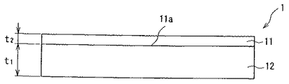
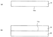
図1は、本発明の実施の形態に係る圧電基板を示す断面図である。図1に示す圧電基板1は、基材11と、基材11の一方の主面上に形成された膜12とから主に構成されている。基材11において、膜12を形成する主面は、鏡面化された主面11aである。
(実施例)
線膨張係数が16.1×10⁻⁶/Kであり、直径4インチ、厚さ0.25mmのタンタル酸リチウム製基板(LT基板)21の一方の主面(裏面)を鏡面化した。なお、鏡面化処理は、コロイダルシリカを用いて研磨機により行った。線膨張係数は、サーモプラス2(株式会社リガク社製)のシステムの熱機械分析装置(TMA−8310)の示差膨張モードにおいて測定した(於工業技術センター)。
図5(a)に示すように、直径4インチ、厚さ約0.5mmのLT基板31の一方の主面(裏面)に直径4インチ、厚さ0.4mmのサファイア基板32を常温接合した。なお、常温接合の際には、LT基板31及びサファイア基板32の接合面をアルゴンイオンビームにより活性化した。次いで、図5(b)に示すように、LT基板31の表面側から研削処理及び/又は研磨処理を行って、LT基板31の厚さを20μmに調整した。
11 基材
11a 主面
12 膜
21 LT基板
22 温度補償膜
23 パターン
24 SAWデバイスチップ
24a くし型電極
Claims (10)
- 10×10-6/K〜20×10-6/Kの線膨張係数を有し、鏡面化された主面を有する基材と、前記主面上に設けられ、前記基材の線膨張係数よりも小さく、−1×10 -6 /K〜10×10 -6 /Kの材料で構成され、5%〜40%の気孔率を有する膜と、を具備することを特徴とする圧電基板。
- 前記膜は、粒子の積層体で構成されていることを特徴とする請求項1記載の圧電基板。
- 前記粒子のサイズが5μm〜300μmであることを特徴とする請求項2記載の圧電基板。
- 前記基材の線膨張係数よりも小さい線膨張係数を有する材料は、Ti、W、Mo、Ta、Si及びこれらの合金、酸化アルミニウム、酸化ケイ素、酸化マグネシウム、酸化ジルコニウム、酸化チタン、炭化ケイ素、炭化ホウ素、窒化アルミニウム、窒化ケイ素及びこれらの化合物の固溶体、並びにこれら金属及び化合物の混合物からなる群より選ばれた少なくとも一つであることを特徴とする請求項1から請求項3のいずれかに記載の圧電基板。
- 前記膜は、0.05mm〜2mmの厚さを有することを特徴とする請求項1から請求項4のいずれかに記載の圧電基板。
- 前記基材は、タンタル酸リチウム、ニオブ酸リチウム、水晶、四ホウ酸リチウム及び酸化亜鉛からなる群より選ばれたもので構成されていることを特徴とする請求項1から請求項5のいずれかに記載の圧電基板。
- 前記基材と前記膜との間にアンダーコートが設けられていることを特徴とする請求項1から請求項6のいずれかに記載の圧電基板。
- 請求項1から請求項7のいずれかに記載の圧電基板と、前記圧電基板の前記鏡面化された主面と反対側の主面上に設けられた素子と、を具備することを特徴とする圧電素子。
- 10×10-6/K〜20×10-6/Kの線膨張係数を有し、鏡面化された主面を有する基材を準備する工程と、前記基材の線膨張係数よりも小さく、−1×10 -6 /K〜10×10 -6 /Kの線膨張係数を有する材料で構成され、5%〜40%の気孔率を有する膜を前記主面上に形成する工程と、を具備することを特徴とする圧電基板の製造方法。
- スラリーを用いたコーティング法により、前記膜を前記基材に形成し、形成した膜を前記基材の支持部材とすることを特徴とする請求項9記載の圧電基板の製造方法。
Priority Applications (3)
| Application Number | Priority Date | Filing Date | Title |
|---|---|---|---|
| JP2007045045A JP4247282B2 (ja) | 2006-07-27 | 2007-02-26 | 圧電基板及びその製造方法 |
| US11/880,168 US7569976B2 (en) | 2006-07-27 | 2007-07-20 | Piezo-electric substrate and manufacturing method of the same |
| EP07014595.8A EP1885062B1 (en) | 2006-07-27 | 2007-07-25 | Piezo-electric substrate and manufacturing method of the same |
Applications Claiming Priority (2)
| Application Number | Priority Date | Filing Date | Title |
|---|---|---|---|
| JP2006204740 | 2006-07-27 | ||
| JP2007045045A JP4247282B2 (ja) | 2006-07-27 | 2007-02-26 | 圧電基板及びその製造方法 |
Related Child Applications (1)
| Application Number | Title | Priority Date | Filing Date |
|---|---|---|---|
| JP2008262370A Division JP4773495B2 (ja) | 2006-07-27 | 2008-10-09 | 圧電素子の製造方法 |
Publications (3)
| Publication Number | Publication Date |
|---|---|
| JP2008054277A JP2008054277A (ja) | 2008-03-06 |
| JP2008054277A5 JP2008054277A5 (ja) | 2008-08-21 |
| JP4247282B2 true JP4247282B2 (ja) | 2009-04-02 |
Family
ID=39237840
Family Applications (1)
| Application Number | Title | Priority Date | Filing Date |
|---|---|---|---|
| JP2007045045A Active JP4247282B2 (ja) | 2006-07-27 | 2007-02-26 | 圧電基板及びその製造方法 |
Country Status (1)
| Country | Link |
|---|---|
| JP (1) | JP4247282B2 (ja) |
Families Citing this family (3)
| Publication number | Priority date | Publication date | Assignee | Title |
|---|---|---|---|---|
| JPWO2010007805A1 (ja) * | 2008-07-17 | 2012-01-05 | 株式会社村田製作所 | 分波器 |
| TW201743176A (zh) * | 2016-05-30 | 2017-12-16 | 日東電工股份有限公司 | 壓電膜 |
| TWI733819B (zh) * | 2016-05-30 | 2021-07-21 | 日商日東電工股份有限公司 | 附透明電極之壓電膜及壓力感測器 |
-
2007
- 2007-02-26 JP JP2007045045A patent/JP4247282B2/ja active Active
Also Published As
| Publication number | Publication date |
|---|---|
| JP2008054277A (ja) | 2008-03-06 |
Similar Documents
| Publication | Publication Date | Title |
|---|---|---|
| US7569976B2 (en) | Piezo-electric substrate and manufacturing method of the same | |
| JP4247281B2 (ja) | 圧電基板及びその製造方法 | |
| EP3490144B1 (en) | Method of producing composite substrate for surface acoustic wave device | |
| JP5833239B2 (ja) | 複合基板、圧電デバイス及び複合基板の製法 | |
| US20100187949A1 (en) | Component with Reduced Temperature Response, and Method for Production | |
| EP2833550B1 (en) | Composite substrate and elastic wave device | |
| JP4723207B2 (ja) | 複合圧電基板 | |
| WO2006120994A1 (ja) | 複合圧電基板 | |
| JP6619327B2 (ja) | 改良型の熱補償形表面弾性波デバイスおよび製造方法 | |
| JP2011087079A (ja) | 弾性表面波素子 | |
| JP4247282B2 (ja) | 圧電基板及びその製造方法 | |
| JP4956569B2 (ja) | 弾性表面波素子 | |
| JP4773494B2 (ja) | 圧電素子の製造方法 | |
| KR100912553B1 (ko) | 압전기판 및 이를 이용한 saw 필터 | |
| JP4773495B2 (ja) | 圧電素子の製造方法 | |
| JP2002151754A (ja) | 圧電体薄膜素子及びその製造方法 | |
| JP2009267665A (ja) | 弾性波素子及びその製造方法 | |
| EP2237417B1 (en) | Elastic wave element and method for manufacturing the same | |
| WO2023017780A1 (ja) | 弾性波装置 | |
| JP2005142902A (ja) | 弾性表面波素子用基板 | |
| JP2008136238A (ja) | 表面波装置及びその製造方法 | |
| JP2009021701A (ja) | 圧電基板の製造方法 | |
| CN116827299A (zh) | 接合基板、弹性波装置及模块 | |
| JP5096695B2 (ja) | 薄膜音響共振器 | |
| JP2009077149A (ja) | 弾性境界波装置 |
Legal Events
| Date | Code | Title | Description |
|---|---|---|---|
| A521 | Request for written amendment filed |
Free format text: JAPANESE INTERMEDIATE CODE: A523 Effective date: 20080703 |
|
| A977 | Report on retrieval |
Free format text: JAPANESE INTERMEDIATE CODE: A971007 Effective date: 20080805 |
|
| A131 | Notification of reasons for refusal |
Free format text: JAPANESE INTERMEDIATE CODE: A131 Effective date: 20080812 |
|
| A521 | Request for written amendment filed |
Free format text: JAPANESE INTERMEDIATE CODE: A523 Effective date: 20081006 |
|
| A131 | Notification of reasons for refusal |
Free format text: JAPANESE INTERMEDIATE CODE: A131 Effective date: 20081104 |
|
| A521 | Request for written amendment filed |
Free format text: JAPANESE INTERMEDIATE CODE: A523 Effective date: 20081110 |
|
| TRDD | Decision of grant or rejection written | ||
| A01 | Written decision to grant a patent or to grant a registration (utility model) |
Free format text: JAPANESE INTERMEDIATE CODE: A01 Effective date: 20090106 |
|
| A01 | Written decision to grant a patent or to grant a registration (utility model) |
Free format text: JAPANESE INTERMEDIATE CODE: A01 |
|
| A61 | First payment of annual fees (during grant procedure) |
Free format text: JAPANESE INTERMEDIATE CODE: A61 Effective date: 20090109 |
|
| R150 | Certificate of patent or registration of utility model |
Ref document number: 4247282 Country of ref document: JP Free format text: JAPANESE INTERMEDIATE CODE: R150 Free format text: JAPANESE INTERMEDIATE CODE: R150 |
|
| FPAY | Renewal fee payment (event date is renewal date of database) |
Free format text: PAYMENT UNTIL: 20120116 Year of fee payment: 3 |
|
| FPAY | Renewal fee payment (event date is renewal date of database) |
Free format text: PAYMENT UNTIL: 20130116 Year of fee payment: 4 |
|
| R250 | Receipt of annual fees |
Free format text: JAPANESE INTERMEDIATE CODE: R250 |
|
| FPAY | Renewal fee payment (event date is renewal date of database) |
Free format text: PAYMENT UNTIL: 20130116 Year of fee payment: 4 |
|
| FPAY | Renewal fee payment (event date is renewal date of database) |
Free format text: PAYMENT UNTIL: 20140116 Year of fee payment: 5 |
|
| R250 | Receipt of annual fees |
Free format text: JAPANESE INTERMEDIATE CODE: R250 |
|
| R250 | Receipt of annual fees |
Free format text: JAPANESE INTERMEDIATE CODE: R250 |
|
| S111 | Request for change of ownership or part of ownership |
Free format text: JAPANESE INTERMEDIATE CODE: R313117 |
|
| S531 | Written request for registration of change of domicile |
Free format text: JAPANESE INTERMEDIATE CODE: R313531 |
|
| R350 | Written notification of registration of transfer |
Free format text: JAPANESE INTERMEDIATE CODE: R350 |
|
| R250 | Receipt of annual fees |
Free format text: JAPANESE INTERMEDIATE CODE: R250 |
|
| R250 | Receipt of annual fees |
Free format text: JAPANESE INTERMEDIATE CODE: R250 |
|
| R250 | Receipt of annual fees |
Free format text: JAPANESE INTERMEDIATE CODE: R250 |
|
| R250 | Receipt of annual fees |
Free format text: JAPANESE INTERMEDIATE CODE: R250 |
|
| R250 | Receipt of annual fees |
Free format text: JAPANESE INTERMEDIATE CODE: R250 |
|
| R250 | Receipt of annual fees |
Free format text: JAPANESE INTERMEDIATE CODE: R250 |
|
| R250 | Receipt of annual fees |
Free format text: JAPANESE INTERMEDIATE CODE: R250 |
|
| R250 | Receipt of annual fees |
Free format text: JAPANESE INTERMEDIATE CODE: R250 |
|
| R250 | Receipt of annual fees |
Free format text: JAPANESE INTERMEDIATE CODE: R250 |
|
| R250 | Receipt of annual fees |
Free format text: JAPANESE INTERMEDIATE CODE: R250 |