JP4244074B2 - Manufacturing method of MONOS type semiconductor nonvolatile memory transistor - Google Patents
Manufacturing method of MONOS type semiconductor nonvolatile memory transistor Download PDFInfo
- Publication number
- JP4244074B2 JP4244074B2 JP06848298A JP6848298A JP4244074B2 JP 4244074 B2 JP4244074 B2 JP 4244074B2 JP 06848298 A JP06848298 A JP 06848298A JP 6848298 A JP6848298 A JP 6848298A JP 4244074 B2 JP4244074 B2 JP 4244074B2
- Authority
- JP
- Japan
- Prior art keywords
- film
- oxide film
- memory
- insulating film
- tunnel insulating
- Prior art date
- Legal status (The legal status is an assumption and is not a legal conclusion. Google has not performed a legal analysis and makes no representation as to the accuracy of the status listed.)
- Expired - Fee Related
Links
Images


Description
【0001】
【発明の属する技術分野】
この発明は、半導体不揮発性メモリトランジスタの製造方法に関し、特にメモリ絶縁膜がトンネル絶縁膜とメモリ窒化膜とトップ酸化膜とからなるいわゆるMONOS(Metal Oxide Nitride Oxide Semiconductor )型と称される半導体不揮発性メモリトランジスタのメモリ特性の向上と信頼性を高める技術に関するものである。
【0002】
【従来の技術】
一般に、MONOS型の半導体不揮発性メモリトランジスタの情報の書き換えは、メモリゲート電極にバイアス電圧を印加することにより、半導体基板からトンネル絶縁膜を通してメモリ窒化膜中およびトンネル絶縁膜とメモリ窒化膜との界面およびメモリ窒化膜とトップ酸化膜との界面に、電子あるいは正孔を注入することにより行なっている。
【0003】
ここで、従来のMONOS型半導体不揮発性メモリトランジスタのNチャネル型トランジスタの構造を、図25に示す模式的な断面図を用いて説明する。
図25に示すように、P型の導電型(第1の導電型)を示す半導体基板1の表面のメモリ素子領域の周辺にフィールド酸化膜2を設け、その半導体基板1のメモリ素子領域上に設けたトンネル絶縁膜31とメモリ窒化膜5とトップ酸化膜6とによってメモリ絶縁膜8を構成し、そのメモリ絶縁膜8上にメモリゲート電極9を設けてMONOS構造を構成している。
【0004】
さらに、半導体基板1のメモリ素子領域には、メモリゲート電極9に自己整合してN型の導電型(第2の導電型)を示す高濃度不純物層からなるソース10とドレイン11を設けている。
そして、この半導体基板1の全面に二酸化シリコン膜を主体とする多層配線用絶縁膜12を設け、その多層配線用絶縁膜12に形成された各コンタクトホール13を介して、ソース10、ドレイン11、および図示していないがメモリゲート電極9にそれぞれ接続する配線14を設けている。
【0005】
このような従来のMONOS型半導体不揮発性メモリトランジスタにおける情報の書き換えは、メモリゲート電極9にバイアス電圧を印加することにより行なう。
すなわち、Nチャネル型のメモリトランジスタの場合には、メモリゲート電極9にプラスのバイアス電圧を印加し、半導体基板1およびソース10とドレイン11を接地することにより、半導体基板1からトンネル絶縁膜31を通してメモリ絶縁膜8に電子を注入し、メモリ窒化膜5中およびトンネル絶縁膜31とメモリ窒化膜5との界面、およびメモリ窒化膜5とトップ酸化膜6との界面に電子を捕獲する。
【0006】
この電子を捕獲したNチャネル型のMONOS型半導体不揮発性メモリトランジスタのしきい値電圧は通常より高くなる。すなわちエンハンスメント動作をする。この場合を書き込み状態と呼ぶ。
【0007】
これとは逆に、メモリゲート電極9を接地し、半導体基板1およびソース10とドレイン11にプラスのバイアス電圧を印加すると、半導体基板1からトンネル絶縁膜31を通してメモリ絶縁膜8に正孔を注入し、メモリ窒化膜5中およびトンネル絶縁膜31とメモリ窒化膜5との界面、およびメモリ窒化膜5とトップ酸化膜6との界面に正孔を捕獲する。
【0008】
この正孔を捕獲したNチャネル型のMONOS型半導体不揮発性メモリトランジスタのしきい値電圧は、通常より低くなる。すなわちディプリーション動作をする。この場合を消去状態と呼ぶ。
このように、MONOS型半導体不揮発性メモリトランジスタは、半導体基板1からトンネル絶縁膜31を介してメモリ絶縁膜8に電子あるいは正孔を注入することにより、書き込み状態あるいは消去状態として情報の書き込みを行なう。
【0009】
なお、Pチャネル型のメモリトランジスタの場合には、バイアス電圧の極性と書き込み状態および消去状態との関係が、上述したNチャネル型のメモリトランジスタの場合と逆になり、正孔を注入したときが書き込み状態で、電子を注入したときが消去状態になる。
いずれにしても、MONOS型半導体不揮発性メモリトランジスタにおける情報の書き換え動作は、トンネル絶縁膜31の膜厚、材料、および膜質に大きく依存する。
【0010】
たとえば、トンネル絶縁膜31の膜厚が厚くなると電子および正孔の半導体基板からの注入効率が低下するため、書き込みスピードの低下と電子および正孔の注入量の低下による捕獲量の低下が生じて情報の書き込みが困難となる。
このため、従来はトンネル絶縁膜31を、シリコン酸化膜を窒化処理することにより形成したシリコン窒化酸化膜によって構成していた。
このシリコン窒化酸化膜の動作を、図26に示すエネルギーバンド図を用いて説明する。
【0011】
図26に示すエネルギーバンド図は、縦方向にエネルギー状態を示し、横方向にMONOS型半導体不揮発性メモリトランジスタのメモリ絶縁膜8の膜構成を示している。
このエネルギーバンド図は、半導体基板1にプラスのバイアス電圧を印加した場合で、Nチャネル型のMONOS型半導体不揮発性メモリトランジスタの消去動作を示しており、膜構成をそのバイアスに応じて傾斜させて示している。
【0012】
メモリ絶縁膜8におけるトンネル絶縁膜31を、破線で示すシリコン酸化膜32で構成する場合には、半導体基板1の正孔に対するシリコン酸化膜32の障壁(図26で下側)は、約3.8eVであり、電子に対するシリコン酸化膜32の障壁(図26で上側)の約3.2eVに比べて高い値を示す。
このため、トンネル絶縁膜31としてシリコン酸化膜32を用いた場合には、一般的に正孔を注入する消去側の書き込みスピードが低下する。
【0013】
このため、消去側のスピードを向上する手段として、メモリ絶縁膜8を構成するトンネル絶縁膜31として、シリコン酸化膜32を窒化処理したシリコン窒化酸化膜を用いることが行なわれている。
すなわち、シリコン酸化膜32に代えて、図26に実線で示すようにシリコン窒化酸化膜3を用いることにより、半導体基板1の正孔に対する障壁(図26で下側)は約3.3eVとなり、シリコン酸化膜32の障壁(約3.8eV)より小さな値となる。この結果、正孔注入効率が向上し、消去動作を速めることができる。
【0014】
しかしながら、メモリ窒化膜5中およびトンネル絶縁膜31とメモリ窒化膜5との界面およびメモリ窒化膜5とトップ酸化膜6との界面に捕獲した正孔から見たトンネル絶縁膜31の障壁も低下するため、正孔が半導体基板1側へ抜けやすくなり、データ保持特性が低下するという問題がある。
Pチャネル型のMONOS型半導体不揮発性メモリトランジスタの場合には、正孔の注入効率が向上することによって、書き込み動作を速めることができるが、捕獲された正孔が半導体基板1側へ抜けやすくなるため、やはりデータ保持特性が低下するという問題がある。
【0015】
【発明が解決しようとする課題】
このように、従来のMONOS型半導体不揮発性メモリトランジスタでも、メモリ絶縁膜を構成するトンネル絶縁膜をシリコン窒化酸化膜にすることにより、消去動作あるいは書き込み動作での正孔の注入効率を向上させ、消去動作あるいは書き込み動作を速くすることはできる。
【0016】
しかしながら、トンネル絶縁膜をシリコン窒化酸化膜にすることにより、消去動作あるいは書き込み動作によって、メモリ絶縁膜のメモリ窒化膜中およびトンネル絶縁膜とメモリ窒化膜との界面、およびメモリ窒化膜とトップ酸化膜との界面に捕獲された正孔から見たトンネル絶縁膜の障壁が低くなり、正孔が半導体基板側へ抜けやすくなるため、データ保持特性が劣化するという問題が生じる。
【0017】
この発明は、このような問題を解決するためになされたものであり、MONOS型半導体不揮発性メモリトランジスタのデータ保持特性を低下させることなく、消去動作あるいは書き込み動作を高速化できるようにすることを目的とする。
そのため、書き換え速度が速くデータ保持特性が良好で、信頼性の高いMONOS型半導体不揮発性メモリトランジスタを容易に製造するの製造方法を提供する。
【0018】
【課題を解決するための手段】
この発明は上記の目的を達成するため、つぎのようなMONOS型半導体不揮発性メモリトランジスタの製造方法を提供する。
【0019】
【0020】
【0021】
すなわち、この発明によるMONOS型半導体不揮発性メモリトランジスタの製造方法は、半導体基板上にトンネル絶縁膜を設け、該トンネル絶縁膜上にメモリ窒化膜を設け、該メモリ窒化膜上にシリコン酸化膜からなるトップ酸化膜を設けて、メモリ絶縁膜とするMONOS型半導体不揮発性メモリトランジスタの製造方法であって、次の各工程を有する。
【0022】
【0023】
【0024】
【0025】
【0026】
【0027】
すなわち、上記半導体基板の表面を一酸化二窒素(N2O)雰囲気中で処理して上記トンネル絶縁膜として機能するシリコン窒化酸化膜を形成する工程と、
それに続いて、上記シリコン窒化酸化膜の表面近傍を酸素雰囲気中で熱処理して、上記メモリ窒化膜側の界面近傍が酸素含有量の多い酸素リッチシリコン窒化酸化膜となるようにする工程と有する。
【0028】
あるいは、上記半導体基板上に酸化処理によりシリコン酸化膜を形成する工程と、
該シリコン酸化膜に窒素イオンを注入した後、酸素を含む窒素雰囲気中で熱処理して、上記半導体基板側の界面近傍では窒素含有量が酸素含有量より多く、上記メモリ窒化膜側の界面近傍では酸素含有量が窒素含有量より多くなるような上記トンネル絶縁膜を形成する工程とを実施するようにしてもよい。
【0029】
または、上記半導体基板上に酸化処理によりシリコン酸化膜を形成する工程と、
該シリコン酸化膜を窒化処理してシリコン窒化酸化膜にし、該シリコン窒化酸化膜の上記メモリ窒化膜側の表面にCVD法により薄膜シリコン酸化膜を形成し、上記トンネル絶縁膜を形成する工程とを実施することもできる。
【0030】
【発明の実施の形態】
以下、この発明の製造方法によって製造するMONOS型半導体不揮発性メモリトランジスタの構造およびその製造方法の最適な実施の形態を図面を用いて詳細に説明する。
【0031】
〔MONOS型半導体不揮発性メモリトランジスタ:図1,図17〕
この発明の製造方法によって製造するMONOS型半導体不揮発性メモリトランジスタの構造を、図1の模式的な断面図を用いて説明する。このMONOS型半導体不揮発性メモリトランジスタは、Nチャネル型半導体装置で示している。
【0032】
図1に示すMONOS型半導体不揮発性メモリトランジスタは、導電型がP型(第1の導電型)の半導体基板1の表面のメモリ素子領域の周辺に、フィールド酸化膜2を設けている。
【0033】
そして、その半導体基板1上にシリコン窒化酸化膜3と酸素リッチシリコン窒化酸化膜4からなるトンネル絶縁膜31を設け、そのトンネル絶縁膜31とその上に設けたメモリ窒化膜5とトップ酸化膜6とによってメモリ絶縁膜8を構成し、その上にメモリゲート電極9を設けている。
【0034】
トンネル絶縁膜31は、酸素と窒素を含むシリコン窒化酸化膜であり、その下層のシリコン窒化酸化膜3はシリコンと酸素と窒素とからなり、窒素の含有量が酸素の含有量より多い絶縁膜である。また、上層の酸素リッチシリコン窒化酸化膜4もシリコンと酸素と窒素とからなり、酸素の含有量が窒素の含有量より多い絶縁膜である。
【0035】
このトンネル絶縁膜31を構成するシリコン窒化酸化膜3と酸素リッチシリコン窒化酸化膜4の具体的な組成比として、X線光電子分光法で求め、
SiOx Ny の組成比として見積もると、
シリコン窒化酸化膜3は、x=0.5、y=0.7 程度、
酸素リッチシリコン窒化酸化膜4は、x=1.1、y=0.3 程度
の組成比の絶縁膜である。
【0036】
さらに、半導体基板1の表面には、メモリゲート電極9に自己整合するように導電型がN型(第2の導電型)の高濃度不純物層からなるソース10とドレイン11を設けている。
そして、全面に二酸化シリコン膜を主体とする多層配線用絶縁膜12を設け、
その多層配線用絶縁膜12に形成された各コンタクトホール13を介してソース10、ドレイン11および図示していないがメモリゲート電極9にそれぞれ接続する配線14を設けている。
【0037】
このMONOS型半導体不揮発性メモリトランジスタは、そのトンネル絶縁膜を、酸素と窒素を含むシリコン窒化酸化膜で構成し、その半導体基板1との界面近傍は窒素含有量が酸素含有量より多いシリコン窒化酸化膜からなり、メモリ窒化膜5との界面近傍のは酸素含有量が窒素含有量より多い酸素リッチシリコン窒化酸化膜からなるようにしたことに特徴がある。
【0038】
これによって、半導体基板の正孔に対するトンネル絶縁膜31の障壁を窒素含有量が多いシリコン窒化酸化膜によって小さくして、メモリ絶縁膜8への正孔注入効率を向上させ、Nチャネル型MONOS型半導体不揮発性メモリトランジスタの消去動作を速くすることができる。
しかし、メモリ窒化膜5中等に捕獲した正孔から見たトンネル絶縁膜31の障壁は、窒素含有量が少ない酸素リッチシリコン窒化酸化膜によって大きいままにして、その正孔が半導体基板側へ抜けにくくしているので、データ保持特性の低下を防止することができる。この作用および効果の詳細は後述する。
【0039】
上述の図1に示したMONOS型半導体不揮発性メモリトランジスタでは、トンネル絶縁膜31の半導体基板1との界面近傍は窒素含有量が酸素含有量より多いシリコン窒化酸化膜3からなり、メモリ窒化膜5との界面近傍は酸素含有量が窒素含有量より多い酸素リッチシリコン窒化酸化膜4からなる。
しかし、この発明によるMONOS型半導体不揮発性メモリトランジスタのトンネル絶縁膜は、この膜構成に限るものではない。
例えば、図17に示すこの発明によるMONOS型半導体不揮発性メモリトランジスタのように、トンネル絶縁膜31を、半導体基板1との界面近傍はシリコン窒化酸化膜3で構成し、メモリ窒化膜5との界面近傍は薄膜シリコン酸化膜41で構成するようにしてもよい。
【0040】
また、上述の例はNチャネル型MONOS型半導体装置の場合の構成を示したが、Pチャネル型半導体装置の場合には、半導体基板1を導電型がN型の半導体基板とし、ソース10およびドレイン11を導電型がP型の高濃度不純物層になるだけであり、その他の構成は図1に示したMONOS型半導体不揮発性メモリトランジスタと同じである。
そして、Pチャネル型MONOS型半導体不揮発性メモリトランジスタの場合は、メモリ絶縁膜8への正孔注入効率を向上させることにより、書き込み動作を速くすることができる。また、メモリ窒化膜5中等に捕獲した正孔が半導体基板側へ抜けにくくして、データ保持特性の低下を防止することができる。
【0041】
〔製造方法の基礎となる例:図1〜図16〕
つぎに、この発明によるMONOS型半導体不揮発性メモリトランジスタの製造方法の基礎となる例を説明する。
まず、図1に示したMONOS型半導体不揮発性メモリトランジスタの製造方法について、図2〜図16と図1によって説明する。図2〜図16は、図1に示したMONOS型半導体不揮発性メモリトランジスタを製造する工程の各段階を順に示す模式的な断面図である。
【0042】
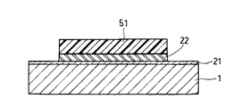
はじめに、図2に示すように、導電型がP型の半導体基板1を酸素と窒素との混合気体中で酸化処理を行ない、厚さ30nmの二酸化シリコン膜からなるパッド酸化膜21を半導体基板1の全面に形成する。
【0043】
つぎに、このパッド酸化膜21上の全面に、ジクロルシラン(SiH2Cl2)とアンモニア(NH3)のガスを用いて、温度740℃でCVD法によって、シリコン窒化膜からなるシリコンナイトライド膜22を、150nm程度の厚さに形成する。
【0044】
そして、図3に示すように、このシリコンナイトライド膜22の全面に感光性材料であるフォトレジスト51を形成し、所定のフォトマスクを用いて露光および現像処理を行ない、メモリ素子領域の周囲のフィールド領域を開口するように、フォトレジスト51をパターンニングする。
【0045】
その後、このフォトレジスト51をエッチングマスクとして、図4に示すように、シリコンナイトライド膜22のフィールド領域の部分をエッチング除去する。このシリコンナイトライド膜22のエッチングは、SF6+CHF3+Heの混合ガスを用いてドライエッチング法により行なう。
そして、エッチングマスクとして用いたフォトレジスト51を除去する。
【0046】
つぎに、半導体基板1およびパッド酸化膜21のメモリ素子領域の周囲のフィールド領域を、シリコンナイトライド膜22を耐酸化マスクにして酸化する。このいわゆる選択酸化処理により、図5に示すようにフィールド領域にフィールド酸化膜2を700nmの厚さで形成する。
この選択酸化処理は、水蒸気酸化雰囲気中で、温度1000℃で酸化処理を行なう。
【0047】
そして、180℃に加熱した熱燐酸(H3PO4)を用いて、シリコンナイトライド膜22を除去し、さらに、フッ酸緩衝液によりパッド酸化膜21をエッチング除去する。図6はこれらの工程によって、シリコンナイトライド膜22とパッド酸化膜21を除去した状態を示す。
【0048】
つぎに、酸素と窒素との混合気体中で酸化処理を行ない、図7に示すように厚さ20nm程度の二酸化シリコン膜からなる犠牲酸化膜23を半導体基板1の全面に形成し、その後、この犠牲酸化膜23をフッ酸緩衝液によりエッチング除去する。
この犠牲酸化膜23の形成と除去は、この後の処理工程で形成するメモリ絶縁膜の信頼性を向上するために行なう。
【0049】
すなわち、前述のように選択酸化処理により素子分離用のフィールド酸化膜2を形成する場合、選択酸化処理中にシリコンナイトライド膜22を構成する窒素と水蒸気雰囲気中の水素とが反応し、アンモニアを形成する。
そのため、パッド酸化膜21と半導体基板1との界面近傍にアンモニアの反応によりシリコン窒化膜が形成され、このシリコン窒化膜が後工程での酸化マスクとして作用し、メモリ絶縁膜の膜厚が不均一となり、信頼性を低下する。この現象を解消するために、犠牲酸化膜23の形成と除去を行なう。
【0050】
つぎに、酸素と窒素との混合気体中で酸化処理を行ない、図8に示すように厚さ2.2nm程度の二酸化シリコン膜からなるシリコン酸化膜24を半導体基板1のメモリ素子領域の全面に形成する。
そして、このシリコン酸化膜24を、温度950℃のアンモニア(NH3)雰囲気中で窒化処理を行ない、図9に示すように半導体基板1のメモリ素子領域の全面にシリコン窒化酸化膜3を形成する。
【0051】
その後、温度900℃の0.2%程度の酸素を含む窒素雰囲気中で、酸化処理を行ない、図10に示すように、シリコン窒化酸化膜3の表面に酸素リッチシリコン窒化酸化膜4を形成し、シリコン窒化酸化膜3と酸素リッチシリコン窒化酸化膜4とからなるトンネル絶縁膜31を形成する。
【0052】
この微量の酸素を含む窒素雰囲気中の処理により、トンネル絶縁膜31は半導体基板1側では酸素含有量より窒素含有量が多いシリコン窒化酸化膜3とし、半導体基板1と接しないトンネル絶縁膜31の上層は窒素含有量の少ない酸素リッチシリコン窒化酸化膜4とすることができる。
【0053】
つぎに図11に示すように、このトンネル絶縁膜31上を含む全面にCVD法により、窒化シリコン膜からなるメモリ窒化膜5を9nm程度の厚さで形成する。このメモリ窒化膜5の形成は、ジクロルシラン(SiH2Cl2)とアンモニア(NH3)のガスを用いて、温度700℃でCVD法によって形成する。
【0054】
さらに、温度950℃の水蒸気酸化雰囲気中で酸化処理を行ない、メモリ窒化膜5を酸化して、このメモリ窒化膜5上に二酸化シリコン膜からなるトップ酸化膜6を形成する。
この酸化処理により、メモリ窒化膜5の膜厚は7nm程度となり、トップ酸化膜6の膜厚は3nm程度となる。
【0055】
そしてさらに、モノシラン(SiH4)のガスを用いて、温度600℃でCVD法によって、多結晶シリコン膜からなるメモリゲート電極材料9bを450nm程度の厚さで全面に形成する。
【0056】
つぎに、全面にフォトレジストを形成した後、所定のフォトマスクを用いて露光および現像処理を行ない、図12に示すようにメモリゲート電極を形成する領域にフォトレジスト52を形成する。
【0057】
その後、このフォトレジスト52をエッチングのマスクとして、メモリゲート電極材料9bである多結晶シリコン膜を、SF6+O2の混合気体をエッチングガスとして用いるドライエッチング法によりエッチングする。
【0058】
ついで、同様にフォトレジスト52をエッチングのマスクとして、トップ酸化膜6とメモリ窒化膜5と酸素リッチシリコン窒化酸化膜4とシリコン窒化酸化膜3とを、CF4+He+CBrF3+O2 の混合気体をエッチングガスとして用いるドライエッチング法によりエッチングする。その後、フォトレジスト52を除去する。
【0059】
その結果、図13に示すように、半導体基板1上に設けたシリコン窒化酸化膜3と酸素リッチシリコン窒化酸化膜4とからなるトンネル絶縁膜31およびメモリ窒化膜5とトップ酸化膜6とによって構成されるメモリ絶縁膜8と、メモリゲート電極9とからなるMONOS構造を構成する。
【0060】
つぎに、メモリゲート電極9をイオン注入のマスクとして用いて、半導体基板1と逆導電型のN型の不純物であるリンを加速エネルギー50keV、イオン注入量3.5×10¹⁵atoms/cm2 程度でイオン注入する。
その結果、同じく図13に示すように、第2導電型のソース10およびドレイン11として半導体基板1にN型の高濃度不純物層を形成する。
【0061】
その後、図14に示すように、全面に二酸化シリコン膜を主体とする多層配線用絶縁膜12を形成する。
そして、N型の高濃度不純物層の活性化と多層配線用絶縁膜12のリフローを兼ねて、窒素雰囲気中で、温度900℃の熱処理を行なう。
さらに、図15に示すように、多層配線用絶縁膜12に接続孔であるコンタクトホールを開口するためのフォトレジスト53を形成する。
【0062】
そして、フォトレジスト53をエッチングマスクにしてコンタクトホール13を図15に示すように設ける。
このコンタクトホール13を形成するためのエッチングは、C2F6+He+CHF3 の混合気体をエッチングガスとして用いるドライエッチング法により行なう。その後、フォトレジスト53を除去する。
【0063】
ついで、図16に示すように、配線材料14bとしてアルミニウムを各コンタクトホール13内を含む全面に設け、その上に配線を形成するためのフォトレジスト54をパターン形成する。
【0064】
その後、フォトエッチング技術を用いて配線材料14bをエッチングする。
このエッチングは、BCl3+CHCl3+Cl2+N2の混合気体をエッチングガスとして用いるドライエッチング法により行ない、図1に示す配線14を形成する。これによって、図1に示したMONOS型半導体不揮発性メモリトランジスタが完成する。
【0065】
つぎに、このMONOS型半導体不揮発性メモリトランジスタの製造方法の他の例を説明する。
以下に述べる他の製造方法において、図2乃至図16によって説明した上述の製造方法と相違するのは、図1に示したMONOS型半導体不揮発性メモリトランジスタのトンネル絶縁膜31を形成する工程だけであり、その他の工程は上述の製造方法と同様であるので、その説明は省略する。
【0066】
この発明の基礎となる他の製造方法によるトンネル絶縁膜の形成工程を、図7から図11を利用して説明する。
図7に示すように半導体基板1上のメモリ素子領域の周辺のフィールド領域にフィールド酸化膜2を形成し、メモリ素子領域に犠牲酸化膜23を形成した後、それを除去する。
【0067】
そして、酸素と窒素との混合気体中で酸化処理を行ない、図8に示すように、膜厚が2.2nm程度の二酸化シリコン膜からなるシリコン酸化膜24を、半導体基板1のメモリ素子領域の全面に形成する。さらに、このシリコン酸化膜24を温度950℃のアンモニア(NH3)雰囲気中で窒化処理を行ない、図9に示すようにシリコン窒化酸化膜3を形成するまでは、前述の製造方法と同様な各工程の処理を行なう。
【0068】
その後、前述の製造方法における酸素を含む窒素雰囲気中での酸化処理に代えて、ランプアニール装置を用いて、温度1000℃の一酸化二窒素(N2O)ガス雰囲気中で、時間20秒の処理を行ない、図10に示すように、シリコン窒化酸化膜3の表面に酸素リッチシリコン窒化酸化膜4を形成する。
それにより、半導体基板1のメモリ素子領域上に、シリコン窒化酸化膜3と酸素リッチシリコン窒化酸化膜4とからなるトンネル絶縁膜31を形成することができる。
【0069】
N2O ガス雰囲気中での処理により、トンネル絶縁膜31は、半導体基板1側では酸素含有量より窒素含有量が多いシリコン窒化酸化膜3であり、半導体基板1と接しないトンネル絶縁膜31の上層は窒素含有量の少ない酸素リッチシリコン窒化酸化膜4とすることができる。
その後、図11に示すように、このトンネル酸化膜31上にメモリ窒化膜5、トップ酸化膜6、およびメモリゲート電極材料9bを順次形成する工程以降は、前述の製造方法の各工程と同じである。
【0070】
〔この発明による製造方法の実施形態〕
つぎに、この発明によるMONOS型半導体不揮発性メモリトランジスタの製造方法の第1の実施形態を、図7,図9および図10を利用して説明する。
図7に示すように、半導体基板1上のメモリ素子領域の周辺のフィールト領域にフィールド酸化膜2を形成し、メモリ素子領域に犠牲酸化膜23を形成した後それを除去する。ここまでは、前述の製造方法と同様な各工程の処理を行なう。
【0071】
そして、犠牲酸化膜23を除去した後、前述の各製造方法の場合のように図8に示したシリコン酸化膜24を形成することなく、直ちにランプアニール装置を用いて、温度1000℃の一酸化二窒素(N2O)ガス雰囲気中で、時間20秒の処理を行い、図9に示すように半導体基板1のメモリ素子領域にシリコン窒化酸化膜3を形成する。
【0072】
その後、連続して同じランプアニール装置を用いて、温度1000℃の酸素雰囲気中で、時間10秒の処理を行ない、図10に示すように、シリコン窒化酸化膜3の表面に酸素リッチシリコン窒化酸化膜4を形成する。
これによって、半導体基板1のメモリ素子領域上に、シリコン窒化酸化膜3と酸素リッチシリコン窒化酸化膜4とからなるトンネル絶縁膜31を形成する。
【0073】
この製造方法によって、トンネル絶縁膜31は、半導体基板1側では酸素含有量より窒素含有量が多いシリコン窒化酸化膜3であり、半導体基板1と接しないトンネル絶縁膜31の上層は窒素含有量の少ない酸素リッチシリコン窒化酸化膜4とすることができる。
これ以後の各工程は、前述の製造方法の各工程と同じである。
【0074】
つぎに、この発明によるMONOS型半導体不揮発性メモリトランジスタの製造方法の第2の実施形態によるトンネル絶縁膜の形成工程を、図8および図10を利用して説明する。
図8に示すように、半導体基板1上のメモリ素子領域の周辺のフィールド領域にフィールド酸化膜2を形成し、その後メモリ素子領域にシリコン酸化膜24を形成するまでは、最初に説明した製造方法と同様な各工程の処理を行なう。
【0075】
そして、図8に示すようにシリコン酸化膜24を形成した後、イオン注入装置を用いて、そのシリコン酸化膜24中に窒素イオンを注入後、酸素を含む窒素雰囲気中で熱処理を行なうことにより、図10に示すようにシリコン窒化酸化膜3の上層を酸素リッチシリコン窒化酸化膜4にしたトンネル絶縁膜31を形成することができる。
【0076】
つぎに、この発明によるMONOS型半導体不揮発性メモリトランジスタの製造方法の第3の実施形態によるトンネル絶縁膜の形成工程を、図17から図20によって説明する。
図7に示したように半導体基板1上のメモリ素子領域の周辺のフィールド領域にフィールド酸化膜2を形成し、メモリ素子領域に犠牲酸化膜23を形成した後、それを除去するまでは、最初に説明した製造方法と同じ各工程を行なう。
【0077】
そして、酸素と窒素との混合気体中で酸化処理を行ない、図18に示すように、二酸化シリコン膜からなるシリコン酸化膜24を、膜厚1.1nm程度に半導体基板1のメモリ素子領域の全面に形成する。この工程も最初に説明した製造方法において、図8によって説明した工程と同様であるが、形成するシリコン酸化膜24の膜厚が、先に説明した製造方法の場合は2.2nm程度であったが、この例の場合にはその約半分の膜厚にする。
【0078】
その後、このシリコン酸化膜24を温度950℃のアンモニア(NH3)雰囲気中で窒化処理を行ない、図19に示すようにシリコン窒化酸化膜3を形成する。このシリコン窒化酸化膜3の膜厚も1.1nm程度になる。
次いで、モノシラン(SiH4)と酸素(O2)とを反応ガスとして用いるCVD法によって、図20に示すように、二酸化シリコン膜からなる薄膜シリコン酸化膜41を、1.2nm程度の厚さでシリコン窒化酸化膜3の全面に形成し、シリコン窒化酸化膜3と薄膜シリコン酸化膜41とからなるトンネル絶縁膜31を形成する。
【0079】
その後、最初の製造方法において図11から図16によって説明した各工程と同様な工程を行うことにより、図17に示したMONOS型半導体不揮発性メモリトランジスタを完成することができる。
【0080】
この製造方法によって作成された、図17のMONOS型半導体不揮発性メモリトランジスタによっても、トンネル絶縁膜31は、半導体基板1側では酸素含有量より窒素含有量が多いシリコン窒化酸化膜3であり、半導体基板1と接しないトンネル絶縁膜31の上層は窒素を含有しない薄膜シリコン酸化膜41となるので、前述の各製造方法によって作られた図1のMONOS型半導体不揮発性メモリトランジスタと同様な効果が得られる。
【0081】
以上の各製造方法の実施形態は、主としてNチャネル型のMONOS型半導体不揮発性メモリトランジスタを製造する場合の例で説明したが、Pチャネル型のMONOS型半導体不揮発性メモリトランジスタを製造する場合には、半導体基板として導電型がN型の半導体基板を使用し、ソースおよびドレインを導電型がP型の高濃度不純物層によって形成するようにすればよい。その他の各工程は上述の各製造方法と同様である。
【0082】
〔この発明の作用効果に係る説明〕
ここで、この発明によって製造したMONOS型半導体不揮発性メモリトランジスタの作用効果を、図21に示すエネルギーバンド図を用いて説明する。
このエネルギーバンド図は、従来例であるトンネル絶縁膜31がシリコン酸化膜32の場合(図中に破線で示す)と、この発明によるトンネル絶縁膜31をシリコン窒化酸化膜3と酸素リッチシリコン窒化酸化膜4で構成した場合(図中に実線で示す)を比較して示してある。
【0083】
図1に示したNチャネル型のMONOS型半導体不揮発性メモリトランジスタでは、消去側のスピードを向上する手法として、トンネル絶縁膜31は、シリコン酸化膜を窒化処理したシリコン窒化酸化膜3を半導体基板1側に設けている。
【0084】
すなわち、図21に示すように、トンネル絶縁膜31の半導体基板1との界面近傍をシリコン窒化酸化膜3とすることにより、半導体基板1の正孔に対する障壁が、破線で示すシリコン酸化膜32の障壁(約3.8eV)より小さな値(約3.3eV)となる。
その結果、正孔注入効率が向上し、消去動作を向上させることができる。
【0085】
さらに、従来は問題となっていた、メモリ窒化膜5中およびトンネル絶縁膜31とメモリ窒化膜5との界面およびメモリ窒化膜5とトップ酸化膜6との界面に捕獲した正孔から見たトンネル絶縁膜31の障壁の低下によるデータ保持特性の低下に関しては、トンネル絶縁膜31のメモリ窒化膜5との界面近傍を酸素リッチシリコン窒化酸化膜4としたことによって解決している。
すなわち、捕獲した正孔から見たトンネル絶縁膜31の障壁は、破線で示すシリコン酸化膜32による障壁と同等な値を示すため、正孔が半導体基板1側へ抜けにくくなって、データ保持特性の低下を防止することができる。
【0086】
また、Pチャネル型のMONOS型半導体不揮発性メモリトランジスタにこの発明を適用した場合には、書き込み効率を向上させ、且つデータ保持特性の低下を防止することができる。
【0087】
すなわち、この発明は、データ保持特性の低下を防ぎながら、消去動作あるいは書き込み動作を速めることができ、MONOS型半導体不揮発性メモリトランジスタの書き換え速度の向上とデータ保持特性の向上を達成することができる。
したがって、信頼性の高い半導体不揮発性素子を提供することができる。
【0088】
つぎに、この本発明による効果を、図22から図24の特性図を用いて説明する。
図22は、本発明の製造方法により作成したMONOS型半導体不揮発性メモリトランジスタと従来の製造方法により作成したMONOS型半導体不揮発性メモリトランジスタの、Nチャネル型トランジスタの場合の情報の書き換え特性を示している。
【0089】
図22の情報の書き換え特性図は、プログラム電圧を7Vとし、横軸にはプログラム時間を対数で示し、縦軸には各プログラム時間におけるしきい値電圧の変化量をΔVthで示しており、電子の注入によるしきい値電圧の上昇動作をプラスで表し、正孔注入によるしきい値電圧の低下動作をマイナスで表している。
ここで、電子の注入によるしきい値電圧の上昇動作を書き込みと呼び、正孔の注入によるしきい値電圧の低下動作を消去と呼ぶ。
【0090】
図22に示すように、トンネル絶縁膜がシリコン酸化膜(図中○印で示す)の場合およびシリコン窒化酸化膜(図中Δ印で示す)の場合の従来例による情報書き換え特性は、トンネル絶縁膜がシリコン酸化膜からなる場合の特性が、特に消去側でのしきい値電圧の変化が遅いという特徴が見られる。
すなわち、情報の書き換え時に消去時間として長時間必要であり、図22で示した例では消去が不可能になっている。
【0091】
この消去時間が長くなるという問題は、先に図26によって説明したように、消去動作が半導体基板からの正孔注入による方法であるため、書き込み時の電子の注入に比較して、半導体基板から見たトンネル絶縁膜の障壁が高く、この障壁を正孔が越える確率が低いために生じる。
【0092】
そのため、他の従来技術では、消去時間を短くするために、トンネル絶縁膜をシリコン窒化酸化膜により構成し、正孔に対する障壁を低下させるという手段がとられている。すなわち、図22に三角点のプロットで示すように、トンネル絶縁膜をシリコン酸化膜からシリコン窒化酸化膜に変えることにより、消去側の特性が向上しており、MONOS型半導体不揮発性メモリトランジスタの情報書き込み動作を高速化できる。
【0093】
トンネル絶縁膜をシリコン窒化酸化膜と酸素リッチシリコン窒化酸化膜とから構成した本発明によるものの特性は、図22に黒丸点のプロットで示すように、従来のシリコン窒化酸化膜でトンネル絶縁膜を形成した場合と同等な書き込み特性を示している。
【0094】
このように、消去側の書き込み特性を向上した場合、従来のシリコン窒化酸化膜のみによるトンネル絶縁膜では、データ保持特性が問題になる。このデータ保持特性の向上効果を図23および図24を用いて説明する。
【0095】
図23と図24は、横軸にはトンネル絶縁膜の条件を、従来のトンネル絶縁膜がシリコン酸化膜の場合とシリコン窒化酸化膜の場合、および本発明による場合を示し、縦軸には、データ保持特性から調べたしきい値電圧の時間に対する傾きであるデータ保持特性の傾き(Decay rate)を示している。
このデータ保持特性の傾きの値が零に近い値であるほど、データ保持特性が良いことを示す。
【0096】
図23は電子を注入した書き込み側の特性を示している。したがって、しきい値電圧は書き込み後、低くなる方向へ時間の経過とともにシフトするため、縦軸のデータ保持特性の傾きはマイナスの値で示している。
【0097】
本発明では、図21のエネルギーバンド図で示したように、窒化処理により膜厚が増加していることと、捕獲した電子から見た障壁もシリコン酸化膜と同等であることから、データ保持特性の傾きが零に近い値を示し、データ保持特性が従来のものと比べて向上している。
【0098】
図24は正孔を注入した消去側の特性を示している。したがって、しきい値電圧は消去後、高くなる方向へ時間の経過とともにシフトするため、縦軸のデータ保持特性の傾きはプラスの値で示している。
【0099】
消去側でも、図21のエネルギーバンド図で示したように、捕獲した正孔から見た障壁が、シリコン窒化酸化膜の場合より大きくなっているため、データ保持特性が向上している。
また、従来のトンネル絶縁膜がシリコン酸化膜の場合には、図22に示したように正孔の注入がほとんどできないため、図24ではシリコン酸化膜の場合のデータを図示していない。
【0100】
このように、消去側の特性を向上するために行なう従来のトンネル絶縁膜をシリコン窒化酸化膜とする構造は、注入した正孔から見たトンネル絶縁膜の障壁も低下し、正孔が半導体基板側へ抜けやすくなり、データ保持特性が劣化するという問題が生じたが、この発明によれば、半導体基板側の障壁は低くして正孔の注入確率を高めて消去特性を向上し、メモリ窒化膜側の障壁は高くして正孔の半導体基板側への抜けを少なくすることによりデータ保持特性を向上する。
Pチャネル型のMONOS型半導体不揮発性メモリトランジスタの場合には、データ保持特性を低下させることなく、書き込み動作を速めることができる。
【0101】
【発明の効果】
以上説明してきたように、この発明の製造方法によれば、データ保持特性が良好で信頼性が高く、且つデータ書き換え速度が速いMONOS型半導体不揮発性メモリトランジスタを、容易に製造することができる。
【図面の簡単な説明】
【図1】 この発明の製造方法によって製造するMONOS型半導体不揮発性メモリトランジスタの完成状態の構造を示す模式的な断面図である。
【図2】 図1に示したMONOS型半導体不揮発性メモリトランジスタの製造方法の一実施形態の最初の数工程を説明するための模式的な断面図である。
【図3】 同じく次の工程を説明するための模式的な断面図である。
【図4】 同じく次の工程を説明するための模式的な断面図である。
【図5】 同じく次の工程を説明するための模式的な断面図である。
【図6】 同じく次の工程を説明するための模式的な断面図である。
【図7】 同じく次の工程を説明するための模式的な断面図である。
【図8】 同じく次の工程を説明するための模式的な断面図である。
【図9】 同じく次の工程を説明するための模式的な断面図である。
【図10】 同じく次の工程を説明するための模式的な断面図である。
【図11】 同じく次の工程を説明するための模式的な断面図である。
【図12】 同じく次の工程を説明するための模式的な断面図である。
【図13】 同じく次の工程を説明するための模式的な断面図である。
【図14】 同じく次の工程を説明するための模式的な断面図である。
【図15】 同じく次の工程を説明するための模式的な断面図である。
【図16】 同じく次の工程を説明するための模式的な断面図である。
【図17】 この発明による他の製造方法で製造されるMONOS型半導体不揮発性メモリトランジスタの完成状態の構造を示す模式的な断面図である。
【図18】 図17に示したMONOS型半導体不揮発性メモリトランジスタの製造方法によってトンネル絶縁膜を形成する最初の工程を説明するための模式的な断面図である。
【図19】 同じく次の工程を説明するための模式的な断面図である。
【図20】 同じく次の工程を説明するための模式的な断面図である。
【図21】 この発明の製造方法によって製造したMONOS型半導体不揮発性メモリトランジスタの作用効果を説明するためのエネルギーバンド図である。
【図22】 この発明の製造方法によって製造したMONOS型半導体不揮発性メモリトランジスタと従来のMONOS型半導体不揮発性メモリトランジスタのプログラム時間としきい値電圧の変化量(ΔVth)の相関特性を示す線図である。
【図23】 この発明の製造方法によって製造したMONOS型半導体不揮発性メモリトランジスタと従来のMONOS型半導体不揮発性メモリトランジスタの書き込み側のデータ保持特性の傾き特性を示す図である。
【図24】 この発明の製造方法によって製造したMONOS型半導体不揮発性メモリトランジスタと従来のMONOS型半導体不揮発性メモリトランジスタの消去側のデータ保持特性の傾き特性を示す図である。
【図25】 従来のMONOS型半導体不揮発性メモリトランジスタの構造を示す模式的な断面図である。
【図26】 従来のMONOS型半導体不揮発性メモリトランジスタのエネルギーバンド図である。
【符号の説明】
1:半導体基板 2:フィールド酸化膜
3:シリコン窒化酸化膜
4:酸素リッチシリコン窒化酸化膜
5:メモリ窒化膜 6:トップ酸化膜
8:メモリ絶縁膜 9:メモリゲート電極
9b:メモリゲート電極材料
10:ソース 11:ドレイン
12:多層配線用絶縁膜
13:コンタクトホール 14:配線
21:パッド酸化膜 22:シリコンナイトライド膜
23:犠牲酸化膜 24,32:シリコン酸化膜
31:トンネル絶縁膜
51,52,53,54:フォトレジスト[0001]
BACKGROUND OF THE INVENTION
The present invention relates to a semiconductor nonvolatile memory transistorTo the manufacturing methodIn particular, the memory characteristics of a semiconductor nonvolatile memory transistor called a MONOS (Metal Oxide Nitride Oxide Semiconductor) type in which the memory insulating film is composed of a tunnel insulating film, a memory nitride film, and a top oxide film are improved and the reliability is improved. It is about technology.
[0002]
[Prior art]
In general, the information in the MONOS type semiconductor nonvolatile memory transistor is rewritten by applying a bias voltage to the memory gate electrode, through the tunnel insulating film from the semiconductor substrate and in the memory nitride film and between the tunnel insulating film and the memory nitride film. In addition, electrons or holes are injected into the interface between the memory nitride film and the top oxide film.
[0003]
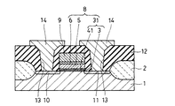
Here, the structure of an N channel type transistor of a conventional MONOS type semiconductor nonvolatile memory transistor will be described with reference to a schematic cross-sectional view shown in FIG.
As shown in FIG. 25, a
[0004]
Further, the memory element region of the
Then, a multilayer
[0005]
Information rewriting in such a conventional MONOS type semiconductor nonvolatile memory transistor is performed by applying a bias voltage to the
That is, in the case of an N-channel type memory transistor, a positive bias voltage is applied to the
[0006]
The threshold voltage of the N-channel MONOS type semiconductor nonvolatile memory transistor that has captured the electrons becomes higher than usual. That is, an enhancement operation is performed. This case is called a write state.
[0007]
On the contrary, when the
[0008]
The threshold voltage of the N-channel MONOS semiconductor nonvolatile memory transistor that captures the holes is lower than usual. That is, a depletion operation is performed. This case is called an erased state.
As described above, the MONOS type semiconductor nonvolatile memory transistor writes information in a writing state or an erasing state by injecting electrons or holes from the
[0009]
In the case of a P-channel memory transistor, the relationship between the polarity of the bias voltage and the writing state and the erasing state is opposite to that of the N-channel memory transistor described above, and holes are injected. When electrons are injected in the written state, the erased state is entered.
In any case, the information rewriting operation in the MONOS type semiconductor nonvolatile memory transistor largely depends on the film thickness, material, and film quality of the
[0010]
For example, when the thickness of the
Therefore, conventionally, the
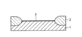
The operation of this silicon oxynitride film will be described with reference to the energy band diagram shown in FIG.
[0011]
The energy band diagram shown in FIG. 26 shows the energy state in the vertical direction and the film configuration of the
This energy band diagram shows an erasing operation of an N-channel MONOS type semiconductor nonvolatile memory transistor when a positive bias voltage is applied to the
[0012]
When the
For this reason, when the
[0013]
Therefore, as a means of improving the speed on the erase side, the memoryInsulation filmA silicon oxynitride film obtained by nitriding the
That is, by using the
[0014]
However, the barrier of
In the case of a P-channel MONOS type semiconductor nonvolatile memory transistor, the hole injection efficiency can be improved to speed up the write operation, but the trapped holes can easily escape to the
[0015]
[Problems to be solved by the invention]
As described above, even in the conventional MONOS type semiconductor nonvolatile memory transistor, by using the silicon nitride oxide film as the tunnel insulating film constituting the memory insulating film, the hole injection efficiency in the erasing operation or the writing operation is improved. The erase operation or the write operation can be speeded up.
[0016]
However, by using a silicon oxynitride film as the tunnel insulating film, the memory nitride film in the memory insulating film and the interface between the tunnel insulating film and the memory nitride film, and the memory nitride film and the top oxide film can be erased or written. The barrier of the tunnel insulating film as viewed from the holes trapped at the interface with the substrate becomes lower, and the holes easily escape to the semiconductor substrate side, which causes a problem that data retention characteristics deteriorate.
[0017]
The present invention has been made to solve such a problem, and it is possible to speed up an erasing operation or a writing operation without deteriorating data retention characteristics of a MONOS type semiconductor nonvolatile memory transistor. Objective.
for that reason, Rewrite speedIs fastData retention characteristicsIs good,reliableMONOS typeSemiconductor non-volatile memory transistorEasy to manufactureA manufacturing method is provided.
[0018]
[Means for Solving the Problems]
In order to achieve the above object, the present invention provides the followingMONOS typeSemiconductor non-volatileManufacturing method of memory transistorI will provide a.
[0019]
[0020]
[0021]
That is,According to this inventionMONOS typeA method for manufacturing a semiconductor nonvolatile memory transistor includes providing a tunnel insulating film on a semiconductor substrate, providing a memory nitride film on the tunnel insulating film, and providing a top oxide film made of a silicon oxide film on the memory nitride film, Memory insulating filmMONOS typeA method for manufacturing a semiconductor nonvolatile memory transistor, comprising the following steps.
[0022]
[0023]
[0024]
[0025]
[0026]
[0027]
That is, the surface of the semiconductor substrate is dinitrogen monoxide (N2O) forming a silicon oxynitride film functioning as the tunnel insulating film by processing in an atmosphere;
Subsequently, the vicinity of the surface of the silicon oxynitride film is heat-treated in an oxygen atmosphere,Memory nitride filmAnd a step of forming an oxygen-rich silicon oxynitride film having a large oxygen content in the vicinity of the side interface.
[0028]
OrForming a silicon oxide film on the semiconductor substrate by an oxidation process;
After nitrogen ions are implanted into the silicon oxide film, heat treatment is performed in a nitrogen atmosphere containing oxygen, so that the nitrogen content is greater than the oxygen content near the interface on the semiconductor substrate side, and near the interface on the memory nitride film side. You may make it implement the process of forming the said tunnel insulating film that oxygen content becomes larger than nitrogen content.
[0029]
Or a step of forming a silicon oxide film on the semiconductor substrate by an oxidation treatment;
Nitriding the silicon oxide film to form a silicon nitride oxide film, forming a thin film silicon oxide film on the surface of the silicon nitride oxide film on the memory nitride film side by a CVD method, and forming the tunnel insulating film; It can also be implemented.
[0030]
DETAILED DESCRIPTION OF THE INVENTION
Hereinafter, this inventionManufactured by the manufacturing methodMONOS type semiconductor nonvolatile memory transistor structure and method of manufacturing the sameWith drawingsThis will be described in detail.
[0031]
[MONOS typeSemiconductor non-volatile memory transistor: FIGS. 1 and 17]
This inventionManufactured by the manufacturing methodMONOS type semiconductor nonvolatile memory transistorStructure ofWill be described with reference to the schematic cross-sectional view of FIG. This MONOS type semiconductor nonvolatile memory transistor is shown as an N-channel type semiconductor device.
[0032]
In the MONOS type semiconductor nonvolatile memory transistor shown in FIG. 1, a
[0033]
A
[0034]
The
[0035]
The specific composition ratio between the
When estimated as the composition ratio of SiOx Ny,
The
The oxygen-rich
An insulating film having a composition ratio of
[0036]
Further, a
Then, an insulating
[0037]
In this MONOS type semiconductor nonvolatile memory transistor, the tunnel insulating film is composed of a silicon oxynitride film containing oxygen and nitrogen, and in the vicinity of the interface with the semiconductor substrate 1IsNitrogen content isConsists of silicon oxynitride film with more oxygen contentNear the interface with the memory nitride film 5Has oxygen contentMore than nitrogen contentOxygen-rich silicon nitride oxide filmThere is a feature in that.
[0038]
As a result, the barrier of the
However, the barrier of the
[0039]
As shown in FIG.MONOS type semiconductor nonvolatile memory transistorThen, the vicinity of the interface between the
However, the tunnel insulating film of the MONOS type semiconductor nonvolatile memory transistor according to the present invention is not limited to this film configuration.
For example, the MONOS type semiconductor nonvolatile memory transistor according to the present invention shown in FIG.likeThe
[0040]
Also, the aboveExampleIs N channel typeMONOS typeIn the case of a P-channel semiconductor device, the
AndPIn the case of a channel type MONOS type semiconductor nonvolatile memory transistor, the write operation can be speeded up by improving the efficiency of hole injection into the
[0041]
[Manufacturing methodBasic example: FIGS. 1 to 16]
Next, a method of manufacturing a MONOS type semiconductor nonvolatile memory transistor according to the present invention will be described.Basic exampleWill be explained.
First, a manufacturing method of the MONOS type semiconductor nonvolatile memory transistor shown in FIG. 1 will be described with reference to FIGS. 2 to 16 are schematic cross-sectional views sequentially showing each stage of the process of manufacturing the MONOS type semiconductor nonvolatile memory transistor shown in FIG.
[0042]
First, as shown in FIG. 2, a
[0043]
Next, dichlorosilane (SiH) is formed on the entire surface of the pad oxide film 21.2Cl2) And ammonia (NH3), A
[0044]
Then, as shown in FIG. 3, a
[0045]
Thereafter, using this
Then, the
[0046]
Next, the field region around the memory element region of the
This selective oxidation treatment is performed at a temperature of 1000 ° C. in a steam oxidation atmosphere.
[0047]
Then, hot phosphoric acid (H3PO4), And the
[0048]
Next, an oxidation process is performed in a mixed gas of oxygen and nitrogen to form a
The formation and removal of the
[0049]
That is, when the
Therefore, a silicon nitride film is formed in the vicinity of the interface between the
[0050]
Next, oxidation treatment is performed in a mixed gas of oxygen and nitrogen, and a
Then, this
[0051]
Thereafter, an oxidation treatment is performed in a nitrogen atmosphere containing about 0.2% oxygen at a temperature of 900 ° C. to form an oxygen-rich silicon
[0052]
By this treatment in a nitrogen atmosphere containing a small amount of oxygen, the
[0053]
Next, as shown in FIG. 11, a
[0054]
Further, oxidation is performed in a steam oxidation atmosphere at a temperature of 950 ° C. to oxidize the
By this oxidation treatment, the thickness of the
[0055]
In addition, monosilane (SiH4), A memory
[0056]
Next, after a photoresist is formed on the entire surface, exposure and development are performed using a predetermined photomask to form a
[0057]
Thereafter, using this
[0058]
Next, similarly, using the
[0059]
As a result, as shown in FIG. 13, the
[0060]
Next, using the
As a result, an N-type high concentration impurity layer is formed on the
[0061]
Thereafter, as shown in FIG. 14, a multilayer
Then, heat treatment at a temperature of 900 ° C. is performed in a nitrogen atmosphere in order to activate the N-type high-concentration impurity layer and to reflow the multilayer
Further, as shown in FIG. 15, a
[0062]
Then, the
Etching to form the
[0063]
Next, as shown in FIG. 16, aluminum is provided as the wiring material 14b on the entire surface including the inside of each
[0064]
Thereafter, the wiring material 14b is etched using a photoetching technique.
This etching is performed using BCl3+ CHCl3+ Cl2+
[0065]
Then thisOther methods for manufacturing a MONOS type semiconductor nonvolatile memory transistorExampleexplain.
Other described belowProduction method2 to 16 described above with reference to FIG.Production methodThe only difference is the step of forming the
[0066]
According to another manufacturing method that forms the basis of the present inventionA tunnel insulating film forming process will be described with reference to FIGS.
As shown in FIG. 7, the periphery of the memory element region on the semiconductor substrate 1Field areaAfter forming the
[0067]
Then, oxidation treatment is performed in a mixed gas of oxygen and nitrogen, and as shown in FIG. 8, a
[0068]
Thereafter, in place of the oxidation treatment in the nitrogen atmosphere containing oxygen in the above-described manufacturing method, a lamp annealing apparatus is used, and a dinitrogen monoxide (N2O) Processing for 20 seconds is performed in a gas atmosphere to form an oxygen-rich
Thereby, the
[0069]
N2By the treatment in the
Thereafter, as shown in FIG. 11, the steps after the step of sequentially forming the
[0070]
[Embodiment of Manufacturing Method According to the Present Invention]
Next,First Embodiment of Manufacturing Method of MONOS Type Semiconductor Nonvolatile Memory Transistor according to the InventionWill be described with reference to FIGS. 7, 9 and 10. FIG.
As shown in FIG. 7, the
[0071]
Then, after the
[0072]
Thereafter, using the same lamp annealing apparatus, a treatment for 10 seconds is performed in an oxygen atmosphere at a temperature of 1000 ° C., and oxygen rich silicon oxynitride is formed on the surface of the
Thus, a
[0073]
In this manufacturing methodThereforeThe
Each process after this is the same as each process of the above-mentioned manufacturing method.
[0074]
Next,Second Embodiment of Manufacturing Method of MONOS Type Semiconductor Nonvolatile Memory Transistor according to the InventionA tunnel insulating film forming step according to FIG. 8 will be described with reference to FIGS.
As shown in FIG. 8, until the
[0075]
Then, after forming the
[0076]
Next,Third Embodiment of Manufacturing Method of MONOS Type Semiconductor Nonvolatile Memory Transistor according to the InventionThe tunnel insulating film formation process byFIG.To FIG.
As shown in FIG. 7, after the
[0077]
Then, oxidation treatment is performed in a mixed gas of oxygen and nitrogen, and as shown in FIG. 18, a
[0078]
Thereafter, the
Next, monosilane (SiH4) And oxygen (O220) as a reactive gas, a thin
[0079]
Then the first manufacturing methodInThe MONOS type semiconductor nonvolatile memory transistor shown in FIG. 17 can be completed by performing the same processes as those described with reference to FIGS.
[0080]
Also in the MONOS type semiconductor nonvolatile memory transistor of FIG. 17 produced by this manufacturing method, the
[0081]
The above embodiments of the manufacturing method have been mainly described with respect to an example of manufacturing an N-channel type MONOS type semiconductor nonvolatile memory transistor, but in the case of manufacturing a P-channel type MONOS type semiconductor nonvolatile memory transistor. The semiconductor substrate may be an N-type semiconductor substrate, and the source and drain may be formed of a high-concentration impurity layer having a P-type conductivity. The other steps are the same as the above-described manufacturing methods.
[0082]
[Explanation related to the effects of the present invention]
Here, in this inventionSo manufacturedThe effect of the MONOS type semiconductor nonvolatile memory transistor will be described with reference to the energy band diagram shown in FIG.
This energy band diagram shows a case where the conventional
[0083]
Figure 1N channel type shownIn the MONOS type semiconductor nonvolatile memory transistor, the
[0084]
That is, as shown in FIG. 21, the vicinity of the interface between the
As a result, the hole injection efficiency is improved, and the erase operation can be improved.
[0085]
Further, the tunnel as viewed from the holes trapped in the
That is, since the barrier of the
[0086]
Also,When the present invention is applied to a P-channel type MONOS type semiconductor nonvolatile memory transistor, it is possible to improve the writing efficiency and prevent the data retention characteristic from deteriorating.
[0087]
That is, the present invention can speed up the erasing operation or the writing operation while preventing the deterioration of the data retention characteristics, and can achieve the improvement of the rewriting speed and the improvement of the data retention characteristics of the MONOS type semiconductor nonvolatile memory transistor. .
Therefore, a highly reliable semiconductor nonvolatile element can be provided.
[0088]
Next, the effect of the present invention will be described with reference to the characteristic diagrams of FIGS.
FIG. 22 shows information rewriting characteristics in the case of an N-channel transistor of a MONOS type semiconductor nonvolatile memory transistor created by the manufacturing method of the present invention and a MONOS type semiconductor nonvolatile memory transistor created by a conventional manufacturing method. Yes.
[0089]
In the information rewrite characteristic chart of FIG. 22, the program voltage is 7 V, the horizontal axis indicates the program time in logarithm, and the vertical axis indicates the amount of change in threshold voltage at each program time by ΔVth. The operation of increasing the threshold voltage due to the injection of hydrogen is represented by plus, and the operation of lowering the threshold voltage due to hole injection is represented by minus.
Here, the operation of increasing the threshold voltage due to electron injection is called writing, and the operation of decreasing the threshold voltage due to hole injection is called erasing.
[0090]
As shown in FIG. 22, the information rewriting characteristics according to the conventional example when the tunnel insulating film is a silicon oxide film (indicated by a circle) and a silicon oxynitride film (indicated by a Δ in the figure) A characteristic in the case where the film is made of a silicon oxide film is characterized in that the change in threshold voltage on the erase side is particularly slow.
That is, a long time is required as an erasing time when rewriting information, and erasing is impossible in the example shown in FIG.
[0091]
As described above with reference to FIG. 26, the problem that the erasing time becomes long is that the erasing operation is a method by hole injection from the semiconductor substrate. This is because the barrier of the tunnel insulating film seen is high and the probability that holes will cross this barrier is low.
[0092]
For this reason, in another conventional technique, in order to shorten the erasing time, the tunnel insulating film is made of a silicon oxynitride film to reduce the barrier against holes. That is, as shown by a plot of triangular points in FIG. 22, the characteristics on the erasing side are improved by changing the tunnel insulating film from the silicon oxide film to the silicon oxynitride film, and the information of the MONOS type semiconductor nonvolatile memory transistor is improved. Write operation can be speeded up.
[0093]
According to the present invention in which the tunnel insulating film is composed of a silicon oxynitride film and an oxygen-rich silicon oxynitride film, the tunnel insulating film is formed of a conventional silicon oxynitride film as shown by a black dot plot in FIG. The same write characteristics as those obtained are shown.
[0094]
As described above, when the erasing side write characteristics are improved, the data retention characteristics become a problem in the conventional tunnel insulating film made of only the silicon oxynitride film. The effect of improving the data retention characteristic will be described with reference to FIGS.
[0095]
23 and 24, the horizontal axis shows the conditions of the tunnel insulating film, the conventional tunnel insulating film is a silicon oxide film and a silicon oxynitride film, and the case according to the present invention, and the vertical axis is The slope of the data retention characteristic (Decay rate), which is the slope of the threshold voltage with respect to time investigated from the data retention characteristic, is shown.
The closer the slope of the data retention characteristic is to zero, the better the data retention characteristic.
[0096]
FIG. 23 shows characteristics on the writing side where electrons are injected. Therefore, since the threshold voltage shifts with time as it decreases after writing, the slope of the data retention characteristic on the vertical axis is indicated by a negative value.
[0097]
In the present invention, as shown in the energy band diagram of FIG. 21, since the film thickness is increased by the nitriding process and the barrier viewed from the captured electrons is equivalent to the silicon oxide film, Shows a value near zero, and the data retention characteristics are improved compared to the conventional one.
[0098]
FIG. 24 shows the characteristics on the erase side where holes are injected. Therefore, since the threshold voltage shifts with time as the time elapses after erasure, the slope of the data retention characteristic on the vertical axis is indicated by a positive value.
[0099]
Even on the erase side, as shown in the energy band diagram of FIG. 21, the barrier viewed from the trapped holes is larger than that of the silicon oxynitride film, so that the data retention characteristics are improved.
Further, when the conventional tunnel insulating film is a silicon oxide film, holes can hardly be injected as shown in FIG. 22, and therefore, data in the case of a silicon oxide film is not shown in FIG.
[0100]
Thus, the structure in which the conventional tunnel insulating film used to improve the characteristics on the erasure side is a silicon oxynitride film reduces the barrier of the tunnel insulating film as seen from the injected holes, and the holes are transferred to the semiconductor substrate. However, according to the present invention, the barrier on the semiconductor substrate side is lowered to increase the probability of hole injection to improve the erasing characteristics, and the memory nitriding The data retention characteristics are improved by increasing the barrier on the film side to reduce the escape of holes to the semiconductor substrate side.
In the case of a P-channel type MONOS type semiconductor nonvolatile memory transistor, the write operation can be speeded up without deteriorating data retention characteristics.
[0101]
【The invention's effect】
As described above, according to the manufacturing method of the present invention, the data retention characteristics are good, the reliability is high, and the data rewriting speed is fast.MONOS typeA semiconductor nonvolatile memory transistor can be easily manufactured.
[Brief description of the drawings]
FIG. 1 of the present inventionMONOS type manufactured by manufacturing methodSemiconductor non-volatile memory transistorCompleted stateIt is typical sectional drawing which shows this structure.
FIG. 2 is shown in FIG.MONOS typeIt is typical sectional drawing for demonstrating the first several process of one Embodiment of the manufacturing method of a semiconductor non-volatile memory transistor.
FIG. 3 is a schematic cross-sectional view for explaining the next step in the same manner.
FIG. 4 is a schematic sectional view for explaining the next step.
FIG. 5 is a schematic cross-sectional view for explaining the next step in the same manner.
FIG. 6 is a schematic sectional view for explaining the next step.
FIG. 7 is a schematic cross-sectional view for explaining the next step in the same manner.
FIG. 8 is a schematic cross-sectional view for explaining the next step in the same manner.
FIG. 9 is a schematic cross-sectional view for explaining the next step in the same manner.
FIG. 10 is a schematic cross-sectional view for explaining the next step in the same manner.
FIG. 11 is a schematic cross-sectional view for explaining the next step in the same manner.
FIG. 12 is a schematic cross-sectional view for explaining the next step in the same manner.
FIG. 13 is a schematic cross-sectional view for explaining the next step in the same manner.
FIG. 14 is a schematic cross-sectional view for explaining the next step in the same manner.
FIG. 15 is a schematic sectional view for explaining the next step in the same manner.
FIG. 16 is a schematic cross-sectional view for explaining the next step in the same manner.
FIG. 17 is according to the present invention.MONOS type manufactured by other manufacturing methodsSemiconductor non-volatile memory transistorCompleted stateIt is typical sectional drawing which shows this structure.
FIG. 18 shows in FIG.MONOS typeIt is typical sectional drawing for demonstrating the first process of forming a tunnel insulating film with the manufacturing method of a semiconductor non-volatile memory transistor.
FIG. 19 is a schematic cross-sectional view for explaining the next step in the same manner.
FIG. 20 is a schematic sectional view for explaining the next step in the same manner.
FIG. 21 shows the present invention.MONOS type manufactured by this manufacturing methodIt is an energy band figure for demonstrating the effect of a semiconductor non-volatile memory transistor.
FIG. 22 shows the present invention.Manufactured by the manufacturing methodFIG. 5 is a diagram showing a correlation characteristic between a program time and a threshold voltage change amount (ΔVth) of a MONOS type semiconductor nonvolatile memory transistor and a conventional MONOS type semiconductor nonvolatile memory transistor.
FIG. 23 shows the present invention.Manufactured by the manufacturing methodIt is a figure which shows the inclination characteristic of the data retention characteristic of the writing side of a MONOS type | mold semiconductor non-volatile memory transistor and the conventional MONOS type | mold semiconductor non-volatile memory transistor.
FIG. 24 shows the present invention.Manufactured by the manufacturing methodIt is a figure which shows the inclination characteristic of the data retention characteristic of the erasing side of a MONOS type | mold semiconductor non-volatile memory transistor and the conventional MONOS type | mold semiconductor non-volatile memory transistor.
FIG. 25 is a schematic cross-sectional view showing the structure of a conventional MONOS type semiconductor nonvolatile memory transistor.
FIG. 26 is an energy band diagram of a conventional MONOS type semiconductor nonvolatile memory transistor.
[Explanation of symbols]
1: Semiconductor substrate 2: Field oxide film
3: Silicon oxynitride film
4: Oxygen-rich silicon oxynitride film
5: Memory nitride film 6: Top oxide film
8: Memory insulating film 9: Memory gate electrode
9b: Memory gate electrode material
10: Source 11: Drain
12: Insulating film for multilayer wiring
13: Contact hole 14: Wiring
21: Pad oxide film 22: Silicon nitride film
23:
31: Tunnel insulating film
51, 52, 53, 54: Photoresist
Claims (3)
前記半導体基板の表面を一酸化二窒素ガス雰囲気中で処理して前記トンネル絶縁膜として機能するシリコン窒化酸化膜を形成する工程と、
該シリコン窒化酸化膜の表面近傍を酸素雰囲気中で熱処理して、前記メモリ窒化膜側の界面近傍が酸素含有量の多い酸素リッチシリコン窒化酸化膜となるようにする工程と、
を有することを特徴とするMONOS型半導体不揮発性メモリトランジスタの製造方法。A MONOS type semiconductor nonvolatile memory in which a tunnel insulating film is provided on a semiconductor substrate, a memory nitride film is provided on the tunnel insulating film, a top oxide film made of a silicon oxide film is provided on the memory nitride film, and a memory insulating film is used. A method for manufacturing a transistor, comprising:
Treating the surface of the semiconductor substrate in a dinitrogen monoxide gas atmosphere to form a silicon oxynitride film functioning as the tunnel insulating film;
Heat treating the vicinity of the surface of the silicon nitride oxide film in an oxygen atmosphere so that the vicinity of the interface on the memory nitride film side becomes an oxygen-rich silicon nitride oxide film having a high oxygen content;
A method for manufacturing a MONOS type semiconductor nonvolatile memory transistor, comprising:
前記半導体基板上に酸化処理によりシリコン酸化膜を形成する工程と、
該シリコン酸化膜に窒素イオンを注入した後、酸素を含む窒素雰囲気中で熱処理して、前記半導体基板側の界面近傍では窒素含有量が酸素含有量より多く、前記メモリ窒化膜側の界面近傍では酸素含有量が窒素含有量より多くなるような前記トンネル絶縁膜を形成する工程と、
を有することを特徴とするMONOS型半導体不揮発性メモリトランジスタの製造方法。A MONOS type semiconductor nonvolatile semiconductor memory device is provided with a tunnel insulating film on a semiconductor substrate, a memory nitride film on the tunnel insulating film, and a top oxide film made of a silicon oxide film on the memory nitride film. A method for manufacturing a memory transistor, comprising:
Forming a silicon oxide film on the semiconductor substrate by oxidation treatment;
After nitrogen ions are implanted into the silicon oxide film, heat treatment is performed in a nitrogen atmosphere containing oxygen, and the nitrogen content is greater than the oxygen content near the interface on the semiconductor substrate side, and near the interface on the memory nitride film side. Forming the tunnel insulating film such that the oxygen content is greater than the nitrogen content;
A method for manufacturing a MONOS type semiconductor nonvolatile memory transistor, comprising:
前記半導体基板上に酸化処理によりシリコン酸化膜を形成する工程と、
該シリコン酸化膜を窒化処理してシリコン窒化酸化膜にし、該シリコン窒化酸化膜の前記メモリ窒化膜側の表面にCVD法により薄膜シリコン酸化膜を形成し、前記トンネル絶縁膜を形成する工程と、
を有することを特徴とするMONOS型半導体不揮発性メモリトランジスタの製造方法。A MONOS type semiconductor nonvolatile semiconductor memory device is provided with a tunnel insulating film on a semiconductor substrate, a memory nitride film on the tunnel insulating film, and a top oxide film made of a silicon oxide film on the memory nitride film. A method for manufacturing a memory transistor, comprising:
Forming a silicon oxide film on the semiconductor substrate by oxidation treatment;
Nitriding the silicon oxide film to form a silicon nitride oxide film, forming a thin film silicon oxide film by a CVD method on the surface of the silicon nitride oxide film on the memory nitride film side, and forming the tunnel insulating film;
A method for manufacturing a MONOS type semiconductor nonvolatile memory transistor, comprising:
Priority Applications (1)
| Application Number | Priority Date | Filing Date | Title |
|---|---|---|---|
| JP06848298A JP4244074B2 (en) | 1997-03-19 | 1998-03-18 | Manufacturing method of MONOS type semiconductor nonvolatile memory transistor |
Applications Claiming Priority (3)
| Application Number | Priority Date | Filing Date | Title |
|---|---|---|---|
| JP6626297 | 1997-03-19 | ||
| JP9-66262 | 1997-03-19 | ||
| JP06848298A JP4244074B2 (en) | 1997-03-19 | 1998-03-18 | Manufacturing method of MONOS type semiconductor nonvolatile memory transistor |
Publications (2)
| Publication Number | Publication Date |
|---|---|
| JPH10321740A JPH10321740A (en) | 1998-12-04 |
| JP4244074B2 true JP4244074B2 (en) | 2009-03-25 |
Family
ID=26407442
Family Applications (1)
| Application Number | Title | Priority Date | Filing Date |
|---|---|---|---|
| JP06848298A Expired - Fee Related JP4244074B2 (en) | 1997-03-19 | 1998-03-18 | Manufacturing method of MONOS type semiconductor nonvolatile memory transistor |
Country Status (1)
| Country | Link |
|---|---|
| JP (1) | JP4244074B2 (en) |
Families Citing this family (12)
| Publication number | Priority date | Publication date | Assignee | Title |
|---|---|---|---|---|
| JP2001093996A (en) | 1999-09-27 | 2001-04-06 | Toshiba Corp | Method of manufacturing semiconductor device |
| JP4923318B2 (en) * | 1999-12-17 | 2012-04-25 | ソニー株式会社 | Nonvolatile semiconductor memory device and operation method thereof |
| KR100386611B1 (en) * | 2000-05-08 | 2003-06-02 | 주식회사 하이닉스반도체 | A array of flash memory cell and method for programming of data thereby and method for erased thereby |
| US6680505B2 (en) | 2001-03-28 | 2004-01-20 | Kabushiki Kaisha Toshiba | Semiconductor storage element |
| KR100395759B1 (en) * | 2001-07-21 | 2003-08-21 | 삼성전자주식회사 | Non-volatile memory device and method of fabricating the same |
| US7057938B2 (en) * | 2002-03-29 | 2006-06-06 | Macronix International Co., Ltd. | Nonvolatile memory cell and operating method |
| JP2004040064A (en) * | 2002-07-01 | 2004-02-05 | Yutaka Hayashi | Nonvolatile memory and method of manufacturing the same |
| JP2006245415A (en) | 2005-03-04 | 2006-09-14 | Sharp Corp | Semiconductor storage device and manufacturing method therefor and portable electronic equipment |
| US7829938B2 (en) * | 2005-07-14 | 2010-11-09 | Micron Technology, Inc. | High density NAND non-volatile memory device |
| JP2007103640A (en) * | 2005-10-04 | 2007-04-19 | Sony Corp | Non-volatile semiconductor memory device |
| JP4997872B2 (en) * | 2006-08-22 | 2012-08-08 | ソニー株式会社 | Nonvolatile semiconductor memory device and manufacturing method thereof |
| WO2009034605A1 (en) * | 2007-09-10 | 2009-03-19 | Renesas Technology Corp. | Nonvolatile semiconductor memory device and method for manufacturing the same |
-
1998
- 1998-03-18 JP JP06848298A patent/JP4244074B2/en not_active Expired - Fee Related
Also Published As
| Publication number | Publication date |
|---|---|
| JPH10321740A (en) | 1998-12-04 |
Similar Documents
| Publication | Publication Date | Title |
|---|---|---|
| JP3312102B2 (en) | Manufacturing method of nonvolatile semiconductor memory device | |
| JPH08228000A (en) | Semiconductor device and manufacture thereof | |
| JP4244074B2 (en) | Manufacturing method of MONOS type semiconductor nonvolatile memory transistor | |
| US6133605A (en) | Semiconductor nonvolatile memory transistor and method of fabricating the same | |
| US6093607A (en) | Method of forming sharp beak of poly by oxygen/fluorine implant to improve erase speed for split-gate flash | |
| JPS5961185A (en) | Manufacture of metal insulator semiconductor field-effect semiconductor device | |
| KR20000069305A (en) | Nonvolatile semiconductor memory device and method of producing the same | |
| JPH04315476A (en) | Method of reducing trap density in oxide film and manufacture of nonvolatile memory cell using same | |
| JPH03257828A (en) | Manufacture of semiconductor device | |
| JP2007142450A (en) | Manufacturing method of nonvolatile semiconductor storage | |
| JP2001148430A (en) | Nonvolatile semiconductor memory | |
| JP2637149B2 (en) | Manufacturing method of nonvolatile semiconductor memory device | |
| JP3924433B2 (en) | Method for manufacturing nonvolatile semiconductor memory device | |
| JPH0888286A (en) | Manufacture of semiconductor memory device | |
| JP3141520B2 (en) | Method for manufacturing nonvolatile memory element | |
| JP2998540B2 (en) | Manufacturing method of nonvolatile semiconductor memory device | |
| JP3283269B2 (en) | Method for manufacturing semiconductor memory device | |
| JP3138538B2 (en) | Semiconductor nonvolatile memory element and method of manufacturing the same | |
| JP3113391B2 (en) | Method for manufacturing semiconductor nonvolatile memory element | |
| JPH098154A (en) | Semiconductor memory device and its manufacture | |
| JPH04246865A (en) | Manufacture of non volatile memory | |
| JP2536866B2 (en) | Method for manufacturing nonvolatile memory element | |
| JPH08293563A (en) | Semiconductor non-volatile memory device and manufacture thereof | |
| JPH09260513A (en) | Semiconductor device and its manufacture | |
| JPH0320088A (en) | Manufacture of semiconductor storage device |
Legal Events
| Date | Code | Title | Description |
|---|---|---|---|
| A521 | Request for written amendment filed |
Free format text: JAPANESE INTERMEDIATE CODE: A523 Effective date: 20050315 |
|
| A621 | Written request for application examination |
Free format text: JAPANESE INTERMEDIATE CODE: A621 Effective date: 20050315 |
|
| A977 | Report on retrieval |
Free format text: JAPANESE INTERMEDIATE CODE: A971007 Effective date: 20080130 |
|
| A131 | Notification of reasons for refusal |
Free format text: JAPANESE INTERMEDIATE CODE: A131 Effective date: 20080722 |
|
| A521 | Request for written amendment filed |
Free format text: JAPANESE INTERMEDIATE CODE: A523 Effective date: 20080922 |
|
| A131 | Notification of reasons for refusal |
Free format text: JAPANESE INTERMEDIATE CODE: A131 Effective date: 20081021 |
|
| A521 | Request for written amendment filed |
Free format text: JAPANESE INTERMEDIATE CODE: A523 Effective date: 20081113 |
|
| TRDD | Decision of grant or rejection written | ||
| A01 | Written decision to grant a patent or to grant a registration (utility model) |
Free format text: JAPANESE INTERMEDIATE CODE: A01 Effective date: 20081224 |
|
| A01 | Written decision to grant a patent or to grant a registration (utility model) |
Free format text: JAPANESE INTERMEDIATE CODE: A01 |
|
| A61 | First payment of annual fees (during grant procedure) |
Free format text: JAPANESE INTERMEDIATE CODE: A61 Effective date: 20081225 |
|
| FPAY | Renewal fee payment (event date is renewal date of database) |
Free format text: PAYMENT UNTIL: 20120116 Year of fee payment: 3 |
|
| FPAY | Renewal fee payment (event date is renewal date of database) |
Free format text: PAYMENT UNTIL: 20140116 Year of fee payment: 5 |
|
| S533 | Written request for registration of change of name |
Free format text: JAPANESE INTERMEDIATE CODE: R313533 |
|
| R350 | Written notification of registration of transfer |
Free format text: JAPANESE INTERMEDIATE CODE: R350 |
|
| LAPS | Cancellation because of no payment of annual fees |