JP4241487B2 - LED driving device, backlight light source device, and color liquid crystal display device - Google Patents
LED driving device, backlight light source device, and color liquid crystal display device Download PDFInfo
- Publication number
- JP4241487B2 JP4241487B2 JP2004124794A JP2004124794A JP4241487B2 JP 4241487 B2 JP4241487 B2 JP 4241487B2 JP 2004124794 A JP2004124794 A JP 2004124794A JP 2004124794 A JP2004124794 A JP 2004124794A JP 4241487 B2 JP4241487 B2 JP 4241487B2
- Authority
- JP
- Japan
- Prior art keywords
- light emitting
- emitting diode
- circuit
- emitting diodes
- transistor
- Prior art date
- Legal status (The legal status is an assumption and is not a legal conclusion. Google has not performed a legal analysis and makes no representation as to the accuracy of the status listed.)
- Expired - Fee Related
Links
Images


Classifications
-
- G—PHYSICS
- G02—OPTICS
- G02F—OPTICAL DEVICES OR ARRANGEMENTS FOR THE CONTROL OF LIGHT BY MODIFICATION OF THE OPTICAL PROPERTIES OF THE MEDIA OF THE ELEMENTS INVOLVED THEREIN; NON-LINEAR OPTICS; FREQUENCY-CHANGING OF LIGHT; OPTICAL LOGIC ELEMENTS; OPTICAL ANALOGUE/DIGITAL CONVERTERS
- G02F1/00—Devices or arrangements for the control of the intensity, colour, phase, polarisation or direction of light arriving from an independent light source, e.g. switching, gating or modulating; Non-linear optics
- G02F1/01—Devices or arrangements for the control of the intensity, colour, phase, polarisation or direction of light arriving from an independent light source, e.g. switching, gating or modulating; Non-linear optics for the control of the intensity, phase, polarisation or colour
- G02F1/13—Devices or arrangements for the control of the intensity, colour, phase, polarisation or direction of light arriving from an independent light source, e.g. switching, gating or modulating; Non-linear optics for the control of the intensity, phase, polarisation or colour based on liquid crystals, e.g. single liquid crystal display cells
- G02F1/133—Constructional arrangements; Operation of liquid crystal cells; Circuit arrangements
-
- G—PHYSICS
- G09—EDUCATION; CRYPTOGRAPHY; DISPLAY; ADVERTISING; SEALS
- G09G—ARRANGEMENTS OR CIRCUITS FOR CONTROL OF INDICATING DEVICES USING STATIC MEANS TO PRESENT VARIABLE INFORMATION
- G09G3/00—Control arrangements or circuits, of interest only in connection with visual indicators other than cathode-ray tubes
- G09G3/20—Control arrangements or circuits, of interest only in connection with visual indicators other than cathode-ray tubes for presentation of an assembly of a number of characters, e.g. a page, by composing the assembly by combination of individual elements arranged in a matrix no fixed position being assigned to or needed to be assigned to the individual characters or partial characters
- G09G3/34—Control arrangements or circuits, of interest only in connection with visual indicators other than cathode-ray tubes for presentation of an assembly of a number of characters, e.g. a page, by composing the assembly by combination of individual elements arranged in a matrix no fixed position being assigned to or needed to be assigned to the individual characters or partial characters by control of light from an independent source
- G09G3/3406—Control of illumination source
-
- G—PHYSICS
- G09—EDUCATION; CRYPTOGRAPHY; DISPLAY; ADVERTISING; SEALS
- G09G—ARRANGEMENTS OR CIRCUITS FOR CONTROL OF INDICATING DEVICES USING STATIC MEANS TO PRESENT VARIABLE INFORMATION
- G09G3/00—Control arrangements or circuits, of interest only in connection with visual indicators other than cathode-ray tubes
- G09G3/20—Control arrangements or circuits, of interest only in connection with visual indicators other than cathode-ray tubes for presentation of an assembly of a number of characters, e.g. a page, by composing the assembly by combination of individual elements arranged in a matrix no fixed position being assigned to or needed to be assigned to the individual characters or partial characters
- G09G3/22—Control arrangements or circuits, of interest only in connection with visual indicators other than cathode-ray tubes for presentation of an assembly of a number of characters, e.g. a page, by composing the assembly by combination of individual elements arranged in a matrix no fixed position being assigned to or needed to be assigned to the individual characters or partial characters using controlled light sources
- G09G3/30—Control arrangements or circuits, of interest only in connection with visual indicators other than cathode-ray tubes for presentation of an assembly of a number of characters, e.g. a page, by composing the assembly by combination of individual elements arranged in a matrix no fixed position being assigned to or needed to be assigned to the individual characters or partial characters using controlled light sources using electroluminescent panels
- G09G3/32—Control arrangements or circuits, of interest only in connection with visual indicators other than cathode-ray tubes for presentation of an assembly of a number of characters, e.g. a page, by composing the assembly by combination of individual elements arranged in a matrix no fixed position being assigned to or needed to be assigned to the individual characters or partial characters using controlled light sources using electroluminescent panels semiconductive, e.g. using light-emitting diodes [LED]
-
- G—PHYSICS
- G09—EDUCATION; CRYPTOGRAPHY; DISPLAY; ADVERTISING; SEALS
- G09G—ARRANGEMENTS OR CIRCUITS FOR CONTROL OF INDICATING DEVICES USING STATIC MEANS TO PRESENT VARIABLE INFORMATION
- G09G3/00—Control arrangements or circuits, of interest only in connection with visual indicators other than cathode-ray tubes
- G09G3/20—Control arrangements or circuits, of interest only in connection with visual indicators other than cathode-ray tubes for presentation of an assembly of a number of characters, e.g. a page, by composing the assembly by combination of individual elements arranged in a matrix no fixed position being assigned to or needed to be assigned to the individual characters or partial characters
- G09G3/34—Control arrangements or circuits, of interest only in connection with visual indicators other than cathode-ray tubes for presentation of an assembly of a number of characters, e.g. a page, by composing the assembly by combination of individual elements arranged in a matrix no fixed position being assigned to or needed to be assigned to the individual characters or partial characters by control of light from an independent source
- G09G3/3406—Control of illumination source
- G09G3/342—Control of illumination source using several illumination sources separately controlled corresponding to different display panel areas, e.g. along one dimension such as lines
-
- H—ELECTRICITY
- H05—ELECTRIC TECHNIQUES NOT OTHERWISE PROVIDED FOR
- H05B—ELECTRIC HEATING; ELECTRIC LIGHT SOURCES NOT OTHERWISE PROVIDED FOR; CIRCUIT ARRANGEMENTS FOR ELECTRIC LIGHT SOURCES, IN GENERAL
- H05B45/00—Circuit arrangements for operating light-emitting diodes [LED]
- H05B45/10—Controlling the intensity of the light
-
- H—ELECTRICITY
- H05—ELECTRIC TECHNIQUES NOT OTHERWISE PROVIDED FOR
- H05B—ELECTRIC HEATING; ELECTRIC LIGHT SOURCES NOT OTHERWISE PROVIDED FOR; CIRCUIT ARRANGEMENTS FOR ELECTRIC LIGHT SOURCES, IN GENERAL
- H05B45/00—Circuit arrangements for operating light-emitting diodes [LED]
- H05B45/20—Controlling the colour of the light
-
- H—ELECTRICITY
- H05—ELECTRIC TECHNIQUES NOT OTHERWISE PROVIDED FOR
- H05B—ELECTRIC HEATING; ELECTRIC LIGHT SOURCES NOT OTHERWISE PROVIDED FOR; CIRCUIT ARRANGEMENTS FOR ELECTRIC LIGHT SOURCES, IN GENERAL
- H05B45/00—Circuit arrangements for operating light-emitting diodes [LED]
- H05B45/30—Driver circuits
- H05B45/37—Converter circuits
- H05B45/3725—Switched mode power supply [SMPS]
-
- H—ELECTRICITY
- H05—ELECTRIC TECHNIQUES NOT OTHERWISE PROVIDED FOR
- H05B—ELECTRIC HEATING; ELECTRIC LIGHT SOURCES NOT OTHERWISE PROVIDED FOR; CIRCUIT ARRANGEMENTS FOR ELECTRIC LIGHT SOURCES, IN GENERAL
- H05B45/00—Circuit arrangements for operating light-emitting diodes [LED]
- H05B45/40—Details of LED load circuits
- H05B45/44—Details of LED load circuits with an active control inside an LED matrix
- H05B45/48—Details of LED load circuits with an active control inside an LED matrix having LEDs organised in strings and incorporating parallel shunting devices
-
- H—ELECTRICITY
- H05—ELECTRIC TECHNIQUES NOT OTHERWISE PROVIDED FOR
- H05B—ELECTRIC HEATING; ELECTRIC LIGHT SOURCES NOT OTHERWISE PROVIDED FOR; CIRCUIT ARRANGEMENTS FOR ELECTRIC LIGHT SOURCES, IN GENERAL
- H05B45/00—Circuit arrangements for operating light-emitting diodes [LED]
- H05B45/50—Circuit arrangements for operating light-emitting diodes [LED] responsive to malfunctions or undesirable behaviour of LEDs; responsive to LED life; Protective circuits
- H05B45/54—Circuit arrangements for operating light-emitting diodes [LED] responsive to malfunctions or undesirable behaviour of LEDs; responsive to LED life; Protective circuits in a series array of LEDs
-
- G—PHYSICS
- G09—EDUCATION; CRYPTOGRAPHY; DISPLAY; ADVERTISING; SEALS
- G09G—ARRANGEMENTS OR CIRCUITS FOR CONTROL OF INDICATING DEVICES USING STATIC MEANS TO PRESENT VARIABLE INFORMATION
- G09G2300/00—Aspects of the constitution of display devices
- G09G2300/04—Structural and physical details of display devices
- G09G2300/0439—Pixel structures
- G09G2300/0452—Details of colour pixel setup, e.g. pixel composed of a red, a blue and two green components
-
- G—PHYSICS
- G09—EDUCATION; CRYPTOGRAPHY; DISPLAY; ADVERTISING; SEALS
- G09G—ARRANGEMENTS OR CIRCUITS FOR CONTROL OF INDICATING DEVICES USING STATIC MEANS TO PRESENT VARIABLE INFORMATION
- G09G2320/00—Control of display operating conditions
- G09G2320/06—Adjustment of display parameters
- G09G2320/0626—Adjustment of display parameters for control of overall brightness
- G09G2320/064—Adjustment of display parameters for control of overall brightness by time modulation of the brightness of the illumination source
-
- G—PHYSICS
- G09—EDUCATION; CRYPTOGRAPHY; DISPLAY; ADVERTISING; SEALS
- G09G—ARRANGEMENTS OR CIRCUITS FOR CONTROL OF INDICATING DEVICES USING STATIC MEANS TO PRESENT VARIABLE INFORMATION
- G09G2330/00—Aspects of power supply; Aspects of display protection and defect management
- G09G2330/08—Fault-tolerant or redundant circuits, or circuits in which repair of defects is prepared
-
- G—PHYSICS
- G09—EDUCATION; CRYPTOGRAPHY; DISPLAY; ADVERTISING; SEALS
- G09G—ARRANGEMENTS OR CIRCUITS FOR CONTROL OF INDICATING DEVICES USING STATIC MEANS TO PRESENT VARIABLE INFORMATION
- G09G2330/00—Aspects of power supply; Aspects of display protection and defect management
- G09G2330/12—Test circuits or failure detection circuits included in a display system, as permanent part thereof
-
- G—PHYSICS
- G09—EDUCATION; CRYPTOGRAPHY; DISPLAY; ADVERTISING; SEALS
- G09G—ARRANGEMENTS OR CIRCUITS FOR CONTROL OF INDICATING DEVICES USING STATIC MEANS TO PRESENT VARIABLE INFORMATION
- G09G2360/00—Aspects of the architecture of display systems
- G09G2360/14—Detecting light within display terminals, e.g. using a single or a plurality of photosensors
- G09G2360/145—Detecting light within display terminals, e.g. using a single or a plurality of photosensors the light originating from the display screen
Description
本発明は、直列接続された発光ダイオード(LED:light emitting diode)をパルス幅変調定電流駆動回路により定電流駆動するようにしたLED駆動装置、このLED駆動装置により駆動されるバックライト光源装置及びカラー液晶表示装置に関する。 The present invention is series-connected light emitting diodes (LED: light emitting diode) LED driving apparatus adapted to constant-current driven by pulse width modulation constant-current driving circuit, a backlight light source device and is driven by the LED driver The present invention relates to a color liquid crystal display device.
近年、液晶TVやプラズマディスプレイ(PDP:Plasma Display Panel)に代表されるようにディスプレイの薄型化が流れとしてあり、中でもモバイル用ディスプレイの多くは液晶系であり、忠実な色の再現性が望まれている。また、液晶パネルのバックライトは蛍光管を使ったCCFL(Cold Cathode Fluorescent Lamp)タイプが主流であるが、環境的に水銀レスが要求されてきており、CCFLに変わる光源として発光ダイオード等が有望視されている。 In recent years, there has been a trend toward thinner displays as represented by LCD TVs and plasma displays (PDPs), and many of the mobile displays are liquid crystal systems, and faithful color reproducibility is desired. ing. In addition, the CCFL (Cold Cathode Fluorescent Lamp) type using a fluorescent tube is the mainstream backlight for liquid crystal panels, but mercury-less has been required environmentally, and light-emitting diodes etc. are promising as a light source to replace CCFL. Has been.
一般的に、発光ダイオードを表示画素に用いたディスプレイでは、発光ダイオードをマトリクスの駆動をするために、各画素に対してX−Yのアドレッシング駆動回路を必要とし、これにより、光らせたい画素の位置にある発光ダイオードを選択(アドレッシング)し、点灯させる時間を変調することにより輝度調整を実施し(パルス幅変調(PWM:Pulse Width Modulation)駆動)、所定の階調性のある表示画面を得ている。このため、駆動用の回路が複雑になりコストが高くなっている(例えば、特許文献1参照)。 Generally, in a display using light emitting diodes as display pixels, in order to drive the light emitting diodes in a matrix, an XY addressing drive circuit is required for each pixel. Select (addressing) the light-emitting diodes in the, and adjust the brightness by modulating the lighting time (pulse width modulation (PWM) drive) to obtain a display screen with a predetermined gradation Yes. This complicates the driving circuit and increases the cost (for example, see Patent Document 1).
ところで、発光ダイオードは、寿命があり、不点灯になるが、個々の素子の壊れ方には、(1)断線してしまうOPENモードによる不良と、(2)短絡してしまうShortモードによる不良と、そのいずれでもなく、(3)光量の低下が発生するモードの3種類に大きくは分類される。 By the way, light-emitting diodes have a lifetime and do not light up, but there are two ways to break down each element: (1) failure due to OPEN mode that causes disconnection and (2) failure due to short mode that causes short circuit. None of them, and (3) a mode in which a decrease in the amount of light occurs is roughly classified into three types.
これらの故障を検出するためには、1つ1つのLED素子を独立した駆動回路で駆動する方法を採用するとともに、個々の素子の動作状態を常にフィードバックするシステムを構築しなければならないので、コストがかさみ、実際の機器では実現が困難であった。 In order to detect these failures, it is necessary to construct a system in which each LED element is driven by an independent drive circuit, and a system that constantly feeds back the operating state of each element must be constructed. It was difficult to realize with actual equipment.
また、発光ダイオードを個別の発光画素に使用した画像表示ディスプレイが存在しているが、その場合のマトリクス型の駆動においても、前述のように、発光ダイオード個々の素子の不良を個別に判断しさらに除去する機能を備えたシステムは、従来、存在していなかった。 In addition, there are image display displays that use light emitting diodes for individual light emitting pixels, but even in matrix-type driving in that case, as described above, it is possible to individually determine the failure of each element of the light emitting diode. A system having a function of removing has not existed conventionally.
発光ダイオードを液晶ディスプレイのバックライトとして使用する場合、個々の発光ダイオードの電力が大きく、個数が比較的少ないため、不良により不点灯箇所が生じると、ムラなどを生じ、見苦しい。また、照明用途のLED駆動装置においては、大電力駆動用のマトリクス駆動LSI等は作成されておらず、現実的にはコスト点で不利であるため、直列接続形式が用いられると考えられるが、直列接続形式では、個々の発光ダイオードの不良が発生し、それが、断線の場合では、一列全てが不点灯となり、著しい色ムラを生じてしまう。 When a light emitting diode is used as a backlight of a liquid crystal display, the power of each light emitting diode is large and the number thereof is relatively small. In addition, in LED driving devices for lighting applications, matrix drive LSIs for high power drive have not been created, and it is actually disadvantageous in terms of cost, so it is considered that a series connection format is used, In the serial connection type, defects of the individual light emitting diodes occur, and in the case of disconnection, all the rows are not lit, resulting in significant color unevenness.
そこで、本発明の目的は、上述の如き従来の実情に鑑み、直列接続された発光ダイオードを定電流駆動するにあたり、発光ダイオードの不良時にその箇所の特定し、不良箇所の素子電流を迂回することのできるLED駆動装置、このLED駆動装置により駆動されるバックライト光源装置及びカラー液晶表示装置を提供することにある。 Therefore, in view of the conventional situation as described above, the object of the present invention is to identify the location when a light emitting diode is defective and to bypass the element current at the defective location when driving the light emitting diode connected in series at a constant current. It is an object of the present invention to provide an LED drive device that can be used , a backlight light source device that is driven by the LED drive device , and a color liquid crystal display device.
本発明の更に他の目的、本発明によって得られる具体的な利点は、以下に説明される実施の形態の説明から一層明らかにされる。 Other objects of the present invention and specific advantages obtained by the present invention will become more apparent from the description of embodiments described below.
本発明は、直列接続された複数の発光ダイオードをパルス幅変調定電流駆動回路により定電流駆動するLED駆動装置であって、上記直列接続された複数の発光ダイオードの各々に並列に接続されたスイッチング素子と、任意の被測定発光ダイオード以外の発光ダイオードに流れる駆動電流をそれぞれスイッチング素子を介してバイパスし、被測定発光ダイオードのみに測定用の駆動電流を流す制御を行う制御回路と、上記被測定発光ダイオードに流れた測定用の駆動電流を検出して、不良箇所の発光ダイオードを特定する検出回路とを備え、上記直列接続された複数の発光ダイオードをパルス幅変調定電流駆動回路により定電流駆動するための主定電流回路と測定用基準定電流回路を上記直列接続された複数の発光ダイオードに切換手段を介して選択的に接続可能としたことを特徴とする。 The present invention, switching to a LED driver for constant current driving a plurality of light emitting diodes connected in series by a pulse width modulation constant-current drive circuit, connected in parallel to each of the plurality of series-connected light emitting diodes a device, and a control circuit for the drive current flowing through the light-emitting diodes other than any of the measured light-emitting diode to bypass through the respective switching elements, performs control to flow a driving current for measurement only to the measured light-emitting diode, the measuring A detection circuit that detects a measurement drive current flowing through the light emitting diode and identifies a light emitting diode at a defective portion, and drives the plurality of light emitting diodes connected in series by a pulse width modulation constant current drive circuit. Switching means for the plurality of light emitting diodes connected in series to the main constant current circuit and the reference constant current circuit for measurement And it is characterized in that a selectively connectable to.
また、本発明は、直列接続された複数の発光ダイオードをパルス幅変調定電流駆動回路により定電流駆動して、表示パネルを背面側から照明するバックライト光源装置であって、上記直列接続された複数の発光ダイオードの各々に並列に接続されたスイッチング素子と、任意の被測定発光ダイオード以外の発光ダイオードに流れる駆動電流をそれぞれスイッチング素子を介してバイパスし、被測定発光ダイオードのみに測定用の駆動電流を流す制御を行う制御回路と、上記被測定発光ダイオードに流れた測定用の駆動電流を検出して、不良箇所の発光ダイオードを特定する検出回路とを備え、上記直列接続された複数の発光ダイオードをパルス幅変調定電流駆動回路により定電流駆動するための主定電流回路と測定用基準定電流回路を上記直列接続された複数の発光ダイオードに切換手段を介して選択的に接続可能としたことを特徴とする。 The present invention also a plurality of light emitting diodes connected in series with constant current drive by a pulse width modulation constant-current driving circuit, a backlight light source device for illuminating the display panel from the back side, which is the series connection A switching element connected in parallel to each of a plurality of light emitting diodes and a drive current flowing through a light emitting diode other than the light emitting diode to be measured are bypassed via the switching elements, and only the light emitting diode to be measured is driven for measurement. A control circuit that controls the flow of current; and a detection circuit that detects a measurement drive current flowing in the light emitting diode to be measured and identifies a light emitting diode at a defective portion, and the plurality of light emitting devices connected in series. The main constant current circuit for driving the diode with the pulse width modulation constant current drive circuit and the reference constant current circuit for measurement are And characterized in that a selectively connectable to a plurality of connected light-emitting diodes via the switching means.
さらに、本発明は、カラーフィルタを備えた透過型のカラー液晶表示パネルと、直列接続された複数の発光ダイオードをパルス幅変調定電流駆動回路により定電流駆動して、上記カラー液晶表示パネルを背面側から照明するバックライト光源装置とからなるカラー液晶表示装置であって、上記バックライト光源装置は、上記直列接続された複数の発光ダイオードの各々に並列に接続されたスイッチング素子と、任意の被測定発光ダイオード以外の発光ダイオードに流れる駆動電流をそれぞれスイッチング素子を介してバイパスし、被測定発光ダイオードのみに測定用の駆動電流を流す制御を行う制御回路と、上記被測定発光ダイオードに流れた測定用の駆動電流を検出して、不良箇所の発光ダイオードを特定する検出回路とを備え、上記直列接続された複数の発光ダイオードをパルス幅変調定電流駆動回路により定電流駆動するための主定電流回路と測定用基準定電流回路を上記直列接続された複数の発光ダイオードに切換手段を介して選択的に接続可能としたことを特徴とする。 Furthermore, the present invention provides a transmissive color liquid crystal display panel provided with a color filter, and a plurality of light emitting diodes connected in series with a constant current drive by a pulse width modulation constant current drive circuit, so that the color liquid crystal display panel is a color liquid crystal display device comprising a backlight light source device for illumination from the side, the backlight light source device, a switching element connected in parallel to each of the plurality of series-connected light emitting diodes, any of the A control circuit that controls the flow of the drive current for measurement only to the light emitting diode to be measured, by bypassing the drive current that flows to the light emitting diode other than the measurement light emitting diode, respectively, and the measurement that has flowed to the light emitting diode to be measured by detecting the driving current of the use, and a detection circuit for identifying the light emitting diode of the defective portion, the series A main constant current circuit and a reference constant current circuit for measurement for driving a plurality of connected light emitting diodes at a constant current by a pulse width modulation constant current driving circuit are selected by switching means to the plurality of light emitting diodes connected in series. It is characterized in that it can be connected .
本発明では、直列接続された複数の素子の各々に並列に接続されたスイッチング素子を介して、任意の被測定発光ダイオード子以外の発光ダイオードに流れる駆動電流をそれぞれバイパスし、被測定発光ダイオードのみに測定用の駆動電流を流す制御を制御回路により行うことによって、上記被測定発光ダイオードに流れた測定用の駆動電流を検出回路により検出して、不良箇所の発光ダイオードを特定することができる。 In the present invention, the drive current flowing through the light emitting diodes other than the light emitting diode elements to be measured is bypassed via the switching elements connected in parallel to each of the plurality of elements connected in series, and only the light emitting diodes to be measured are bypassed. When the control circuit controls the flow of the measurement drive current, the detection drive current flowing in the light emitting diode to be measured can be detected by the detection circuit, and the light emitting diode at the defective portion can be specified.
また、本発明では、上記直列接続された複数の発光ダイオードをパルス幅変調定電流駆動回路により定電流駆動するための主定電流回路と測定用基準定電流回路を上記直列接続された複数の発光ダイオードに切換手段を介して選択的に接続可能としたことにより、測定用基準定電流回路から測定用基準定電流を流して、上記発光ダイオードの不良を検出することができる。 In the present invention, the main constant current circuit for driving the plurality of light emitting diodes connected in series by the pulse width modulation constant current driving circuit and the reference constant current circuit for measurement are the plurality of light emitting elements connected in series. Since the diode can be selectively connected via the switching means, the measurement reference constant current can be supplied from the measurement reference constant current circuit to detect the defect of the light emitting diode.
さらに、上記制御回路により、上記検出回路により特定された不良箇所の素子に並列に接続されている上記トランジスタからなるスイッチング素子を上記パルス幅変調定電流駆動回路によるPWM駆動と同期して動作させて、不良箇所の素子に流れる駆動電流を常時バイパスさせる制御を行うことによって、不良箇所の素子電流をスイッチング素子を介してバイパスすることができる。 Further, the control circuit causes the switching element composed of the transistor connected in parallel to the element at the defective location specified by the detection circuit to operate in synchronization with the PWM drive by the pulse width modulation constant current drive circuit. By performing control to always bypass the drive current flowing through the defective element, the defective element current can be bypassed via the switching element.
以下、本発明の実施の形態について、図面を参照して詳細に説明する。なお、本発明は以下の例に限定されるものではなく、本発明の要旨を逸脱しない範囲で、任意に変更可能であることは言うまでもない。 Hereinafter, embodiments of the present invention will be described in detail with reference to the drawings. Needless to say, the present invention is not limited to the following examples, and can be arbitrarily changed without departing from the gist of the present invention.
本発明は、例えば図1に示すような構成のバックライト方式のカラー液晶表示装置100に適用される。
The present invention is applied to a backlight type color liquid
このカラー液晶表示装置100は、透過型のカラー液晶表示パネル10と、このカラー液晶表示パネル10の背面側に設けられたバックライト光源装置20からなる。
The color liquid
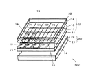
透過型のカラー液晶表示パネル10は、ガラス等の構成された2枚の透明な基板(TFT基板11、対向電極基板12)を互いに対向配置させ、その間隙に例えばツイステッドネマチック(TN)液晶を封入した液晶層13を設けた構成となっている。TFT基板11にはマトリクス状に配置された信号線14と走査線15及びこれらの交点に配置されたスイッチング素子としての薄膜トランジスタ16と画素電極17が形成されている。薄膜トランジスタ16は走査線15により順次選択されると共に、信号線14から供給される映像信号を対応する画素電極17に書き込む。一方、対向電極基板12の内表面には対向電極18及びカラーフィルタ19が形成されている。
In the transmissive color liquid
このカラー液晶表示装置100では、この様な構成の透過型のカラー液晶表示パネル10を2枚の偏光板31,32で挟み、バックライト光源装置20により背面側から白色光を照射した状態で、アクティブマトリクス方式で駆動することによって、所望のフルカラー 映像表示が得られる。
In this color liquid
上記バックライト光源装置20は、光源21と波長選択フィルタ22からなり、上記光源21が出射する光で上記波長選択フィルタ22を介して上記カラー液晶表示パネル10を背面側から照明する。
The backlight
このカラー液晶表示装置100は、例えば図2に電気的なブロック構成を示す駆動回路200により駆動される。
The color liquid
この駆動回路200は、カラー液晶表示パネル10やバックライト光源装置20の駆動電源を供給する電源部110、カラー液晶表示パネル10を駆動するXドライバ回路120及びYドライバ回路130、外部から映像信号が入力端子140を介して供給されるRGBプロセス処理部150、このRGBプロセス処理部150に接続された映像メモリ160及び制御部170、バックライト光源装置20の駆動制御するバックライト駆動制御部180等を備えてなる。
The
この駆動回路200において、入力端子140を介して入力された映像信号は、RGBプロセス処理部150によりクロマ処理等の信号処理がなされ、さらに、コンポジット信号からカラー液晶表示パネル10の駆動に適したRGBセパレート信号に変換されて、制御部170に供給されるとともに、画像メモリ160を介してXドライバ120に供給される。また、制御部170は、上記RGBセパレート信号に応じた所定のタイミングでXドライバ120及びYドライバ回路130を制御して、上記画像メモリ160を介してXドライバ120に供給されるRGBセパレート信号でカラー液晶表示パネル10を駆動することにより、上記RGBセパレート信号に応じた映像を表示する。
In this
ここで、カラーフィルタ19は各画素電極17に対応した複数のセグメントに分割されている。例えば、図3の(A)に示すように3原色である赤色フィルタCFR、緑色フィルタCFG、青色フィルタCFBの3つのセグメント、図3の(B)に示すように3原色(RGB)にシアン(C)を加えた赤色フィルタCFR、シアン色フィルタCFC、緑色フィルタCFG、青色フィルタCFBの4つのセグメント、あるいは、図3の(C)に示すように3原色(RGB)にシアン(C)とイエロー(Y)を加えた赤色フィルタCFR、シアン色フィルタCFC、青色フィルタCFG、イエロー色フィルタCFY、青色フィルタCFBの5つのセグメントに分割されている。
Here, the
ここで、上記バックライト光源装置20には、透過型のカラー液晶表示パネル10を背面に配設された複数の発光ダイオード(LED:light emitting diode)により照射するエリアライト方式の光源21が採用されている。
Here, the backlight
このバックライト光源装置20の光源21における発光ダイオードの配置について説明する。
The arrangement of the light emitting diodes in the
図4は、発光ダイオードの配置例として、単位セル4−1,4−2毎に、赤の発光ダイオード1、緑の発光ダイオード2及び青の発光ダイオード3をそれぞれ2個使用し、合計6個の発光ダイオードを一列に配列した様子を示している。
FIG. 4 shows an example of the arrangement of the light emitting diodes, using two red
この配置例では6個であるが、使用する発光ダイオードの定格、発光効率などにより、混合色をバランスの良い白色光とするために、光出力バランスを整える必要から、各色の個数配分は本例以外のバリエーションがありうる。 In this arrangement example, there are six. However, in order to make the mixed color white light with a good balance according to the rating of the light emitting diode to be used, light emission efficiency, etc., it is necessary to adjust the light output balance. There can be other variations.
図4に示した配置例において、上記単位セル4−1と単位セル4−2は、全く同一の物であり、中央の両端矢印部分で接続されている。また、図5は、上記単位セル4−1及び単位セル4−2が接続された形を電気回路図記号のダイオードマークによって図示したものである。この例の場合、各発光ダイオード、すなわち、赤の発光ダイオード1、緑の発光ダイオード2、青の発光ダイオード3は左から右に電流が流れる方向に極性を合わせて直列接続されている。
In the arrangement example shown in FIG. 4, the unit cell 4-1 and the unit cell 4-2 are exactly the same, and are connected by a double-ended arrow portion at the center. Further, FIG. 5 shows a shape in which the unit cell 4-1 and the unit cell 4-2 are connected by a diode mark of an electric circuit diagram symbol. In this example, each light-emitting diode, that is, red light-emitting
ここで、赤の発光ダイオード1、緑の発光ダイオード2及び青の発光ダイオード3をそれぞれ2個使用し、合計6個の発光ダイオードを一列に配列した単位セル4を各色の発光ダイオードの個数でパターン表記すると図6に示すように(2G 2R 2B)となる。すなわち、(2G 2R 2B)は、緑と赤と青2個ずつ合計6個のパターンを基本単位としていることを示す。そして、図7に示すように、上記基本単位の単位セル4を3つ連続に繋げた場合、記号が3*(2G 2R 2B)で、発光ダイオードの個数でパターン表記すると(6G 6R 6B)で示される。
Here, two red
次に、上記バックライト光源装置20の光源21における実際の発光ダイオードの配置例を図7の表記に基づき説明する。
Next, an actual arrangement example of light emitting diodes in the
光源21には、図8に示すように、前述した発光ダイオードの基本単位(2G 2R 2B)の3倍を1つの中単位(6G 6R 6B)として、垂直に4行、水平に5列、合計で360個の発光ダイオードが配置されている。
As shown in FIG. 8, the
そして、上記360個の発光ダイオード全てに対して、個々のアドレッシングを施すことは容易でないので、このバックライト光源装置20では、図9に示すような駆動構成としている。
Since it is not easy to perform individual addressing on all the 360 light emitting diodes, the backlight
すなわち、n列のそれぞれに対応するRGBのペアg1〜gnは、各列にRGBの各発光ダイオードそれぞれが独立して直列接続されており、DC−DCコンバータ7により定電流が流される構成となっている。
That is, the RGB pairs g1 to gn corresponding to each of the n columns are configured such that each of the RGB light emitting diodes is independently connected in series to each column, and a constant current is passed by the DC-
図10を参照して、定電流をLED直列接続基板m1,m2に流すための具体的な構成例の説明をする。 With reference to FIG. 10, a specific configuration example for flowing a constant current through the LED series connection substrates m1 and m2 will be described.
すなわち、複数の発光ダイオードLED1〜LEDnが直列接続されたLED列40は、一端が検出抵抗(Rc)5を介してDC−DCコンバーター7に接続され、また、他端がFET6を介して接地されている。
That is, the
上記DC−DCコンバーター7は、出力電圧Vccの設定に対して、検出抵抗5による電圧降下を検出して、直列接続されたLED列に所定の定電流ILEDが流れるようにフィードバックループを構成している。この例では、上記検出抵抗5による降下電圧が上記DC−DCコンバーター7内に設けられたサンプルホールド回路を介して帰還される。
The DC-
なお、この例では、定電流を波高値で制御するために、電流検出のフィードバックループにサンプルホールドを備えているが、これはひとつの例であって、他の方法を用いてもよい。 In this example, in order to control the constant current with the peak value, the current detection feedback loop is provided with a sample hold, but this is one example, and other methods may be used.
また、上記バックライト駆動制御部180に備えられたドライバーIC181からFET6のゲートに加えられるmain PWM(Pulse Width Modulation)信号により、LED列40に流れる電流が所定の期間ON−OFFされることにより、発光ダイオードの発光量を増減せしめる構成となっている。
In addition, a current PWM (Pulse Width Modulation) signal applied to the gate of the
すなわち、このバックライト光源装置20では、上記バックライト駆動制御部180に備えられたドライバーIC181から供給されるmain PWM信号によりFET6をスイッチング動作させて、複数の発光ダイオードLED1〜LEDnを直列接続してなるLED列40にDC−DCコンバーター7により供給された駆動電流をOn−OFFすることによって、上記発光ダイオードLED1〜LEDnをパルス幅変調定電流駆動するようになっている。
That is, in the backlight
また、この構成例では、上記LED列40に測定用基準定電流を流すため測定用基準定電流回路であるDC−DCコンバータと、上記DC−DCコンバータ70に接続された検出抵抗(Rref)50と、切換スイッチ60を備え、上記LED列40の一端が上記切換スイッチ60を介して、上記LED列40に駆動電流を流すため主定電流回路である上記DC−DCコンバータ7と、上記LED列40に測定用基準定電流を流すため測定用基準定電流回路であるDC−DCコンバータ70に選択的に接続されるようになっている。
Further, in this configuration example, a DC-DC converter which is a measurement reference constant current circuit for causing a measurement reference constant current to flow through the
さらに、上記発光ダイオードLED1〜LEDnには、各々にスイッチング素子SW1〜SWnが並列に接続されており、、上記直列接続された複数の発光ダイオードLED1〜LEDnに流れる駆動電流を個別に上記スイッチング素子SW1〜SWnを介してバイパスすることができるようになっている。 Further, switching elements SW1 to SWn are connected in parallel to the light emitting diodes LED1 to LEDn, respectively, and the driving currents flowing through the plurality of light emitting diodes LED1 to LEDn connected in series are individually switched to the switching elements SW1. It can be bypassed via SWn.
このように、直列接続された複数の発光ダイオードLED1〜LEDnをパルス幅変調定電流駆動回路により定電流駆動するにあたり、上記直列接続された複数の発光ダイオードLED1〜LEDnに流れる駆動電流を個別にスイッチング素子SW1〜SWnを介してバイパス可能としたことにより、発光ダイオードの個々の不良を検出することができる。 As described above, when the plurality of light emitting diodes LED1 to LEDn connected in series are driven with constant current by the pulse width modulation constant current driving circuit, the drive currents flowing through the plurality of light emitting diodes LED1 to LEDn connected in series are individually switched. By enabling bypassing through the elements SW1 to SWn, individual defects of the light emitting diode can be detected.
ここで、通常の点灯時における駆動電流供給する主定電流回路である上記DC−DCコンバータ7は、比較的電圧が高い多数個の発光ダイオードLED1〜LEDnが直列接続されたLED列40を駆動する関係で、耐圧を必要とし、構成部品形状が大きい。これに対して、上記スイッチング素子SW1〜SWnを使用して、個々の発光ダイオードLED1〜LEDnに基準電流IrefLEDを流す際には、図11に示すように、発光ダイオードを1つだけ点灯させればよいので、電圧は非常に低くてよい。上記DC−DCコンバータ7を非常に低電圧まで動作可能な構成とするのは非効率なので、切換スイッチ60を介して上記LED列40に測定用基準定電流を流すため測定用基準定電流回路であるDC−DCコンバータ70を接続するようにしている。
Here, the DC-
このDC−DCコンバーター70は、出力電圧Vtestの設定に対して、検出抵抗(Rref)50による電圧降下を検出し、所定の定電流(IrefLED)が流れるようにフィードバックループを構成している。
This DC-
また、DC−DCコンバータ70から基準電流IrefLEDを供給する際には、FET6は常時ONとされている。
Further, when the reference current IrefLED is supplied from the DC-
なお、この図10及び図11に示した一群のLED列40は、図9に示したn列のそれぞれに対応するRGBのペアg1〜gnの1列に対している。したがって、同様の回路が、本例では、gn列×3倍(RGB分)必要となる。
The group of
図10及び図11に示した一群のLED列40におけるLED41の個数は、光量バランスの観点で個数は変動するので種々のケースが考えられる。特に、近年、総個数を削減する為に各素子の投入電力を大きくしているため、各素子の輝度特性のばらつきを検出して調整により克服する必要がある。
Since the number of
ここで、上記スイッチング素子SW1〜SWnにはトランジスタを用いることができ、上記トランジスタのベースに供給するスイッチング制御信号により、上記直列接続された複数の発光ダイオードLED1〜LEDnに流れる駆動電流を個別に上記トランジスタからなるスイッチング素子SW1〜SWnを介してバイパスする制御を行うことができる。 Here, transistors can be used for the switching elements SW1 to SWn, and the drive currents flowing through the plurality of light emitting diodes LED1 to LEDn connected in series are individually determined by the switching control signal supplied to the base of the transistors. Bypass control can be performed through the switching elements SW1 to SWn made of transistors.
例えば図12に示す構成では、直列接続された5個の発光ダイオード41A〜41Eに個々に並列にスイッチング素子としてトランジスタ82A〜82Eが接続されており、各トランジスタ82A〜82Eのベース・エミッタ間にはクランプ用のダイオード83A〜83Eが接続され、さらに、各トランジスタ82A〜82Eのベースに結合用コンデンサ84A〜84Eが接続されている。
For example, in the configuration shown in FIG. 12,
直列接続された5個の発光ダイオード41A〜41Eには、上から下に向けて、各々Vfa〜Vfeまでの、個別の電圧降下を有しており、製造ロットに応じてばらつきを持つ。また、直列接続された5個の発光ダイオード41A〜41EはFET6によってPWM駆動されている。
The five light-emitting diodes 41A to 41E connected in series have individual voltage drops from Vfa to Vfe from the top to the bottom, and vary depending on the production lot. The five light emitting diodes 41A to 41E connected in series are PWM driven by the
このような構成の駆動回路において、各トランジスタ82A〜82Eの各ベースには、上記バックライト駆動制御部180に備えられた駆動制御回路182からスイッチング制御信号として結合用コンデンサ84A〜84Eを介してsub_PWM信号a〜eが供給される。上記結合用コンデンサ84A〜84Eに入力されるsub_PWM信号a〜eは、ダイオード83A〜83Eによってトランジスタ82A〜82Eのエミッタ電位がクランプされるため、交流信号として扱うことができる。したがって、直列接続であっても電位を考えずに、トランジスタ82A〜82EのON−OFF駆動ができる。
In the drive circuit having such a configuration, the bases of the
例えば発光ダイオード41Aに並列接続されたトランジスタ82AがONすると、ダイオード41Aのアノード−カソード間はトランジスタ82Aのオン抵抗にて短絡バイパスされ、発光ダイオード41Aの駆動電流の全てがトランジスタ82Aに流れ、発光ダイオード41Aは不点灯となる。
For example, when the
ここで、図12に示した構成例における動作の一例を図13を参照して説明する。 Here, an example of the operation in the configuration example shown in FIG. 12 will be described with reference to FIG.
図13において、(a)〜(b)は縦列接続された5つのトランジスタ82A〜82Eのベースに加えられるsub_PWM信号a〜eの波形を示している。又、t1,t2,t3,t4,t5はその時間軸上のタイミングを示している。
In FIG. 13, (a) to (b) show waveforms of sub_PWM signals a to e applied to the bases of five
今、t1の時点では、sub_PWM信号aのみが低レベルであり、トランジスタ82Aはoffしている。t1時にはトランジスタ82B〜82Eは全てONしており、これにより、発光ダイオード41Aのみが点灯する。
At time t1, only the sub_PWM signal a is at a low level, and the
同様にして、t2の時点には発光ダイオード41B,t3の時点には発光ダイオード41C,t4の時点には発光ダイオード41D,t5の時点には発光ダイオード41Eと順次個別に点灯させることができる。ここでは、5個の縦列接続を例としているが、これは、任意の個数n個の場合も同様である。バイパスする時間をOn−OFFの期間比率の操作により加減すれば、分流する電流の精度があがり、測定時間も確保可能である。
Similarly, the light emitting diode 41B can be turned on individually at the time t2, the
トランジスタ駆動用に使用するsub_PWM信号a〜eは、main_PWM信号と独立して選択することが可能な構成となっているため、自由度が高い。また、sub_PWM信号a〜eの周波数を上げることにより、点灯時間を非常に短くすることができ、素早い点灯が可能である。 The sub_PWM signals a to e used for driving the transistor have a configuration that can be selected independently of the main_PWM signal, and thus have a high degree of freedom. Further, by increasing the frequency of the sub_PWM signals a to e, the lighting time can be shortened very quickly, and quick lighting is possible.
次に、上述の(3)光量の低下が発生するモードのLED不良の検出について説明する。 Next, the detection of LED failure in the above-described (3) mode in which the light amount is reduced will be described.
上述の(3)光量の低下が発生するモードのLED不良は、発光ダイオードの発光量を測定する検出することができる。 The above-mentioned (3) LED failure in the mode in which the light amount is reduced can be detected by measuring the light emission amount of the light emitting diode.
そこで、参照して、バックライト光源装置20における発光ダイオードの発光量を測定するための構成例を図14に示す。
Therefore, referring to FIG. 14, a configuration example for measuring the light emission amount of the light emitting diode in the backlight
このバックライト光源装置20では、上述した一連の説明による動作により、任意個別の発光ダイオードを選択点灯可能である。そこで、上記複数の発光ダイオードが発光した光を受光して光量を検出する光センサを設け、測定用の駆動電流を流す被測定発光ダイオードを順次選択し、上記光センサによる検出出力に基づいて、上記複数の発光ダイオードの発光量のばらつきを測定することができる。
In the backlight
例えば、図14に示す構成例は、直接接続された複数の発光ダイオードLED1〜LEDnから発光された光を受光する光センサであるフォトダイオード185を備える。
For example, the configuration example shown in FIG. 14 includes a
フォトダイオード185の検出出力は演算増幅器186Aにより構成された電流電圧変換回路186を介してA/D変換器187に供給されデジタルデータとしてマイクロプロセッサ188に供給されるようになっている。
The detection output of the
上記マイクロプロセッサ188は、上記直列接続された複数の発光ダイオードLED1〜LEDnに接続されたFET6をスイッチグ制御することによってPWM駆動するためのドライバーIC181及び上記直列接続された複数の発光ダイオードLED1〜LEDnにそれぞれ並列接続されたスイッチング素子SW1〜SWnにスイッチグ制御信号を供給する駆動制御回路182に対し、バス189を介して駆動設定制御信号を与え、上記FET6を常時オンにした状態で、任意の被測定発光ダイオード以外の発光ダイオードに流れる駆動電流をそれぞれスイッチング素子を介してバイパスし、被測定発光ダイオードのみに測定用の駆動電流を流す制御を行い、測定用の駆動電流を流す被測定発光ダイオードを順次選択し、上記光センサによる検出出力に基づいて、上記複数の発光ダイオードの発光量のばらつきを測定する。
The microprocessor 188 includes a
すなわち、上記マイクロプロセッサ188は、任意の発光ダイオードを選択し、その発光ダイオードを非常に短い時間(例えば1μ秒)点灯させ、その値をフォトダイオード185により検出してメモリに記憶する。発光ダイオードが選択されるのは非常にわずかな時間であるので、例えば本例のように、360個の発光ダイオードが有り、個別に1μ秒の時間を要したとしても、合計は360μ秒ということになる。
That is, the microprocessor 188 selects an arbitrary light emitting diode, lights up the light emitting diode for a very short time (for example, 1 μsec), detects the value by the
なお、発光ダイオードを液晶用バックライト光源として使用する場合には、必ずしも、光センサは発光ダイオードの近傍に配置できず、配置上の制約と形状の制約を受ける。この際、形状により、離れたい位置に存在する発光ダイオードは弱く検出され、センサーに近い位置にある発光ダイオードの光は強く検出されるという場合がある。これらは、光学シュミレーションや基準発光ダイオードによる実測等により、補正値データーをメモリテーブルとして用意し、光学センスした光量データーを補正すること等で対応することができる。 When a light emitting diode is used as a backlight light source for a liquid crystal, the optical sensor cannot necessarily be disposed in the vicinity of the light emitting diode, and is subject to arrangement restrictions and shape restrictions. At this time, depending on the shape, there are cases where the light-emitting diodes present at positions desired to be separated are detected weakly, and the light from the light-emitting diodes located near the sensor is detected strongly. These can be dealt with by preparing correction value data as a memory table by optical simulation or actual measurement using a reference light emitting diode, and correcting optically sensed light quantity data.
ここで、発光ダイオードは長時間使用により輝度特性が劣化し発光量が少なくなる特性を有するので、発光量を維持するために駆動電流を徐々に増やすのでは寿命が短くなってしまうが、発光ダイオードの輝度特性についての経時変化を考慮した補正値データをメモリテーブルにようしておき、上記マイクロプロセッサ188により駆動電流を時間とともに減らす制御を行うようにすれば、発光ダイオードの寿命を延ばすことができる。 Here, since the light emitting diode has the characteristic that the luminance characteristic deteriorates and the light emission amount decreases with long-term use, if the drive current is gradually increased in order to maintain the light emission amount, the life is shortened. If the correction value data considering the change with time in the luminance characteristic is stored in a memory table and the microprocessor 188 performs control to reduce the drive current with time, the life of the light emitting diode can be extended. .
この構成例では、任意の発光ダイオードを駆動させ、発光出力データーを測定・記憶・補正することが可能であるので、光量が異常に低下した個別の発光ダイオードの識別が可能である。 In this configuration example, any light emitting diode can be driven to measure, store, and correct the light emission output data, so that it is possible to identify individual light emitting diodes whose light amount is abnormally reduced.
次に、不良モードとして前述した (1)断線してしまうOPENモードによる不良の回避方法について図15乃至図17を参照して説明する。 Next, a method of avoiding a defect in the OPEN mode described above as (1) disconnection will be described with reference to FIGS. 15 to 17.
図15に示す構成例では、上記直列接続された複数の発光ダイオードLED1〜LEDnに流れた駆動電流を検出して、不良箇所の発光ダイオードを特定する検出回路90が次のように設けられている。
In the configuration example shown in FIG. 15, a
すなわち、検出回路90は、上記直列接続された複数の発光ダイオードLED1〜LEDnとPWM駆動用のFET6との接続点が分圧抵抗91,92を介して接地され、また、上記FET6のゲートが分圧抵抗93,94を介して接地されており、上記分圧抵抗91,92の接続中点Pに得られる電圧と、上記分圧抵抗91,92の接続中点Qに得られる電圧をエクスクルーシブORゲート95で比較することにより不良箇所の発光ダイオードを特定する構成となっている。
That is, in the
この検出回路90において、上記FET6はゲートに与えられるmain_PWM信号に応じてスイッチング動作を行っているので、上記直列接続された複数の発光ダイオードLED1〜LEDnが正常な場合は、上記分圧抵抗91,92の接続中点Pに得られる電圧と、上記分圧抵抗91,92の接続中点Qに得られる電圧の変化が逆相になっており、エクスクルーシブORゲート95の出力は、常に論理”1”(Hiレベル)となっている。
In the
そして、上記直列接続された複数の発光ダイオードLED1〜LEDnのどれか1つがOPENした場合、P点の電位は常にLoレベルになるため、エクスクルーシブORゲート95の出力はmain_PWM信号と同様の矩形波になる。
When any one of the plurality of light emitting diodes LED1 to LEDn connected in series is opened, the potential at the point P is always at the Lo level, so that the output of the exclusive OR
上記マイクロプロセッサ188は、この矩形波になることを検出した場合、上記駆動制御回路182を制御して、図16のフローチャートに示す手順に従って、上記直列接続された複数の発光ダイオードLED1〜LEDnにそれぞれ並列接続されたスイッチング素子SW1〜SWnを順次オンさせていくことによって、上記エクスクルーシブORゲート95の出力が論理”1”(Hiレベル)となった時のnが、故障箇所であると特定することができる。
When the microprocessor 188 detects that this rectangular wave is detected, the microprocessor 188 controls the
すなわち、上記マイクロプロセッサ188は、オンにするスイッチング素子SW1〜SWnを示すスイッチ番号nをn=0すなわち全てのスイッチング素子SW1〜SWnをオフ状態とするように初期設定し(ステップS1)、エクスクルーシブORゲート95の出力が常に論理”1”(Hiレベル)となっている正常状態であるか、main_PWM信号と同様の矩形波になっている異常状態であるか判定する(ステップS2)。
That is, the microprocessor 188 initializes the switch number n indicating the switching elements SW1 to SWn to be turned on so that n = 0, that is, all the switching elements SW1 to SWn are turned off (Step S1). It is determined whether the output of the
上記エクスクルーシブORゲート95の出力が正常状態である場合には、スイッチ番号nがn=0すなわち全てのスイッチング素子SW1〜SWnがオフ状態とされているか否かを判定する(ステップS3)。
When the output of the exclusive OR
このステップS3における判定結果がYESすなわち全てのスイッチング素子SW1〜SWnがオフ状態とされている場合には、上記ステップS2に戻ってエクスクルーシブORゲート95の出力を繰り返し判定する。
If the determination result in step S3 is YES, that is, if all the switching elements SW1 to SWn are turned off, the process returns to step S2 to repeatedly determine the output of the exclusive OR
また、上記ステップS2における判定の結果、上記エクスクルーシブORゲート95の出力が異常状態である場合には、番号nをインクリメント(n=n+1)して(ステップS4)、スイッチング素子SWnをオンして(ステップS4)、上記ステップS2に戻ってエクスクルーシブORゲート95の出力を判定する処理を繰り返し行う。
If the result of determination in step S2 is that the output of the exclusive OR
そして、上記ステップS2における判定の結果、上記エクスクルーシブORゲート95の出力が正常状態になると、上記ステップS3に移ってスイッチ番号nがn=0であるか否かの判定を行い、上記エクスクルーシブORゲート95の出力が正常状態になった時点でのスイッチ番号nで示されるスイッチング素子SWnが並列接続されている発光ダイオードLEDnがOPENモードの不良であると特定する(ステップS6)。
As a result of the determination in step S2, when the output of the exclusive OR
そして、上記マイクロプロセッサ188は、今、仮にn=3すなわち3番目の発光ダイオードが故障(OPEN)と特定された場合、図17に示すように、故障個所とされた3番目の発光ダイオード41Cは不良の認識がなされ、この発光ダイオード41Cに並列に接続されているスイッチング素子であるトランジスタ82Cには、上記FET6と同様のメインPWM信号をスイッチング制御信号として与え、並列に同期してON-OFFさせることにより、不良の認識がなされた発光ダイオード41Cに流れる駆動電流を上記トランジスタ82Cを介してバイパスすることができる。
Then, if n = 3, that is, if the third light-emitting diode is specified as a failure (OPEN), the microprocessor 188 determines that the third light-emitting
次に、不良モードとして前述した、 (2)短絡してしまうShortモードによる不良の回避方法について説明する。ショートしてしまった場合、この構成例では、定電流制御の関係で、自動的にDC−DCコンバーター7の出力電圧Vsetがダイオード1個分の電圧低下をして、電気回路としては、正常に働く。また、前述した光学的検出機構を設けた場合は、故障した発光ダイオードを特定することができる。又、ショート不良は、あくまで異常時の状態であるため、経過的に(1)断線してしまうOPENモードに状態が変質・移行することがある。その場合、前述の手法で対処することができる。
Next, a description will be given of a method for avoiding a defect in the short mode, which has been described above as the failure mode. In the case of a short circuit, in this configuration example, the output voltage Vset of the DC-
1,2,3,41,41A〜41E、LED1〜LEDn 発光ダイオード、4−1,4−2 単位セル、5,50 検出抵抗、7,70 DC−DCコンバーター、6 FET、10 カラー液晶表示パネル、11 TFT基板、12 対向電極基板、13 液晶層、14 信号線、15 走査線、16 薄膜トランジスタ、17 画素電極、18 対向電極、19 カラーフィルタ、20 バックライト光源装置、21 光源21、22 波長選択フィルタ、31,32 偏光板、40 LED列、50 切換スイッチ、82A〜82E トランジスタ、83A〜83E ダイオード、84A〜84E コンデンサ、100 カラー液晶表示装置、110 電源部、120 Xドライバ回路、130 Yドライバ回路、140 入力端子140、150 RGBプロセス処理部、160 映像メモリ、170 制御部、180 バックライト駆動制御部、181 ドライバーIC、182 駆動制御回路、185 フォトダイオード、186 電流電圧変換回路、186A 演算増幅器、187 A/D変換器、188 マイクロプロセッサ、200 駆動回路、SW1〜SWn スイッチング素子
1, 2, 3, 41, 41A to 41E, LED1 to LEDn Light emitting diode, 4-1, 4-2 unit cell, 5,50 detection resistor, 7,70 DC-DC converter, 6 FET, 10 color liquid crystal display panel , 11 TFT substrate, 12 Counter electrode substrate, 13 Liquid crystal layer, 14 Signal line, 15 Scan line, 16 Thin film transistor, 17 Pixel electrode, 18 Counter electrode, 19 Color filter, 20 Back light source device, 21
Claims (12)
上記直列接続された複数の発光ダイオードの各々に並列に接続されたスイッチング素子と、
任意の被測定発光ダイオード以外の発光ダイオードに流れる駆動電流をそれぞれスイッチング素子を介してバイパスし、被測定発光ダイオードのみに測定用の駆動電流を流す制御を行う制御回路と、
上記被測定発光ダイオードに流れた測定用の駆動電流を検出して、不良箇所の発光ダイオードを特定する検出回路と
を備え、
上記直列接続された複数の発光ダイオードをパルス幅変調定電流駆動回路により定電流駆動するための主定電流回路と測定用基準定電流回路を上記直列接続された複数の発光ダイオードに切換手段を介して選択的に接続可能としたLED駆動装置。 An LED driving device for driving a plurality of light emitting diodes connected in series with a constant current driving circuit by a pulse width modulation constant current driving circuit,
A switching element connected in parallel to each of the plurality of light emitting diodes connected in series;
A control circuit for performing a control for bypassing a drive current flowing in a light emitting diode other than a light emitting diode to be measured through a switching element, and flowing a driving current for measurement only in the light emitting diode to be measured;
A detection circuit for detecting a measurement drive current flowing in the light emitting diode to be measured and identifying a light emitting diode at a defective portion;
With
A main constant current circuit for driving the plurality of light emitting diodes connected in series by a pulse width modulation constant current driving circuit and a reference constant current circuit for measurement to the plurality of light emitting diodes connected in series via a switching means. LED drive device that can be selectively connected.
上記制御回路は、上記トランジスタのベースに上記コンデンサを介してスイッチング制御信号を供給することにより、上記直列接続された複数の発光ダイオードに流れる駆動電流を個別に上記トランジスタからなるスイッチング素子を介してバイパスする制御を行う請求項2記載のLED駆動装置。 A diode connected between the base and emitter of the transistor, and a capacitor connected to the base of the transistor;
The control circuit supplies a switching control signal to the base of the transistor through the capacitor, thereby bypassing the drive current flowing through the plurality of light emitting diodes connected in series individually through the switching element including the transistor. The LED driving device according to claim 2, wherein control is performed .
上記直列接続された複数の発光ダイオードの各々に並列に接続されたスイッチング素子と、
任意の被測定発光ダイオード以外の発光ダイオードに流れる駆動電流をそれぞれスイッチング素子を介してバイパスし、被測定発光ダイオードのみに測定用の駆動電流を流す制御を行う制御回路と、
上記被測定発光ダイオードに流れた測定用の駆動電流を検出して、不良箇所の発光ダイオードを特定する検出回路と
を備え、
上記直列接続された複数の発光ダイオードをパルス幅変調定電流駆動回路により定電流駆動するための主定電流回路と測定用基準定電流回路を上記直列接続された複数の発光ダイオードに切換手段を介して選択的に接続可能としたバックライト光源装置。 A backlight light source device that illuminates a display panel from the back side by driving a plurality of light emitting diodes connected in series with a constant current by a pulse width modulation constant current driving circuit,
A switching element connected in parallel to each of the plurality of light emitting diodes connected in series;
A control circuit for performing a control for bypassing a drive current flowing in a light emitting diode other than a light emitting diode to be measured through a switching element, and flowing a driving current for measurement only in the light emitting diode to be measured;
A detection circuit for detecting a measurement drive current flowing in the light emitting diode to be measured and identifying a light emitting diode at a defective portion;
With
A main constant current circuit for driving the plurality of light emitting diodes connected in series by a pulse width modulation constant current driving circuit and a reference constant current circuit for measurement to the plurality of light emitting diodes connected in series via a switching means. Backlight light source device that can be selectively connected .
上記制御回路は、上記トランジスタのベースに上記コンデンサを介してスイッチング制御信号を供給することにより、上記直列接続された複数の発光ダイオードに流れる駆動電流を個別に上記トランジスタからなるスイッチング素子を介してバイパスする制御を行う請求項6記載のバックライト光源装置。 A diode connected between the base and emitter of the transistor, and a capacitor connected to the base of the transistor;
The control circuit supplies a switching control signal to the base of the transistor through the capacitor, thereby bypassing the drive current flowing through the plurality of light emitting diodes connected in series individually through the switching element including the transistor. The backlight light source device according to claim 6 which performs control to perform .
上記バックライト光源装置は、上記直列接続された複数の発光ダイオードの各々に並列に接続されたスイッチング素子と、任意の被測定発光ダイオード以外の発光ダイオードに流れる駆動電流をそれぞれスイッチング素子を介してバイパスし、被測定発光ダイオードのみに測定用の駆動電流を流す制御を行う制御回路と、上記被測定発光ダイオードに流れた測定用の駆動電流を検出して、不良箇所の発光ダイオードを特定する検出回路とを備え、上記直列接続された複数の発光ダイオードをパルス幅変調定電流駆動回路により定電流駆動するための主定電流回路と測定用基準定電流回路を上記直列接続された複数の発光ダイオードに切換手段を介して選択的に接続可能としたカラー液晶表示装置。 A transmissive color liquid crystal display panel provided with a color filter and a backlight for illuminating the color liquid crystal display panel from the back side by driving a plurality of light emitting diodes connected in series with a constant current by a pulse width modulation constant current drive circuit A color liquid crystal display device comprising a light source device,
The backlight light source device bypasses a switching element connected in parallel to each of the plurality of light emitting diodes connected in series and a driving current flowing through a light emitting diode other than a light emitting diode to be measured via the switching element. And a control circuit for controlling the measurement drive current to flow only to the light emitting diode to be measured, and a detection circuit for detecting the measurement drive current flowing to the light emitting diode to be measured and identifying the light emitting diode at the defective portion A main constant current circuit for driving the plurality of light emitting diodes connected in series by a pulse width modulation constant current driving circuit and a reference constant current circuit for measurement in the plurality of light emitting diodes connected in series. A color liquid crystal display device which can be selectively connected via a switching means.
上記制御回路は、上記トランジスタのベースに上記コンデンサを介してスイッチング制御信号を供給することにより、上記直列接続された複数の発光ダイオードに流れる駆動電流を個別に上記トランジスタからなるスイッチング素子を介してバイパスする制御を行う請求項10記載のカラー液晶表示装置。 A diode connected between the base and emitter of the transistor, and a capacitor connected to the base of the transistor;
The control circuit supplies a switching control signal to the base of the transistor through the capacitor, thereby bypassing the drive current flowing through the plurality of light emitting diodes connected in series individually through the switching element including the transistor. The color liquid crystal display device according to claim 10, wherein control is performed .
Priority Applications (6)
| Application Number | Priority Date | Filing Date | Title |
|---|---|---|---|
| JP2004124794A JP4241487B2 (en) | 2004-04-20 | 2004-04-20 | LED driving device, backlight light source device, and color liquid crystal display device |
| TW094110107A TWI265465B (en) | 2004-04-20 | 2005-03-30 | Constant current driving device, backlight light source device, and color liquid crystal display device |
| KR1020050029025A KR101146196B1 (en) | 2004-04-20 | 2005-04-07 | Constant current driving device, backlight light source device, and color liquid crystal display device |
| US11/107,124 US7425943B2 (en) | 2004-04-20 | 2005-04-15 | Constant current driving device, backlight light source device, and color liquid crystal display device |
| EP05252411A EP1589519B1 (en) | 2004-04-20 | 2005-04-19 | Constant current driving device, backlight light source device, and color liquid crystal display device |
| CNB2005100660708A CN100397466C (en) | 2004-04-20 | 2005-04-20 | Constant current driving device, backlight light source device, and color liquid crystal display device |
Applications Claiming Priority (1)
| Application Number | Priority Date | Filing Date | Title |
|---|---|---|---|
| JP2004124794A JP4241487B2 (en) | 2004-04-20 | 2004-04-20 | LED driving device, backlight light source device, and color liquid crystal display device |
Publications (2)
| Publication Number | Publication Date |
|---|---|
| JP2005310998A JP2005310998A (en) | 2005-11-04 |
| JP4241487B2 true JP4241487B2 (en) | 2009-03-18 |
Family
ID=34940891
Family Applications (1)
| Application Number | Title | Priority Date | Filing Date |
|---|---|---|---|
| JP2004124794A Expired - Fee Related JP4241487B2 (en) | 2004-04-20 | 2004-04-20 | LED driving device, backlight light source device, and color liquid crystal display device |
Country Status (6)
| Country | Link |
|---|---|
| US (1) | US7425943B2 (en) |
| EP (1) | EP1589519B1 (en) |
| JP (1) | JP4241487B2 (en) |
| KR (1) | KR101146196B1 (en) |
| CN (1) | CN100397466C (en) |
| TW (1) | TWI265465B (en) |
Cited By (1)
| Publication number | Priority date | Publication date | Assignee | Title |
|---|---|---|---|---|
| US9456486B2 (en) | 2010-03-18 | 2016-09-27 | Koninklijke Philips N.V. | Method and apparatus for increasing dimming range of solid state lighting fixtures |
Families Citing this family (163)
| Publication number | Priority date | Publication date | Assignee | Title |
|---|---|---|---|---|
| JP4123183B2 (en) * | 2004-04-20 | 2008-07-23 | ソニー株式会社 | Constant current drive device, backlight light source device, and color liquid crystal display device |
| KR100985859B1 (en) * | 2004-04-27 | 2010-10-08 | 삼성전자주식회사 | Liquid crystal display apparatus and control method thereof |
| US20060288827A1 (en) * | 2005-04-28 | 2006-12-28 | Mitsubishi Heavy Industrial, Ltd. | Method and device for cutting off band-like paper member and controller of the device |
| JP4438599B2 (en) * | 2004-10-26 | 2010-03-24 | 住友電気工業株式会社 | Optical transmitter |
| JP4904783B2 (en) * | 2005-03-24 | 2012-03-28 | ソニー株式会社 | Display device and display method |
| JP5414141B2 (en) * | 2005-04-18 | 2014-02-12 | 株式会社東芝 | Information processing device |
| US20080150439A1 (en) * | 2005-04-29 | 2008-06-26 | O2Micro. Inc. | Serial powering of an light emitting diode string |
| EP1935038B1 (en) * | 2005-09-30 | 2017-07-26 | Seoul Viosys Co., Ltd | Light emitting device having vertically stacked light emitting diodes |
| DE602006021218D1 (en) * | 2005-11-08 | 2011-05-19 | Koninkl Philips Electronics Nv | CIRCUIT ARRANGEMENT AND METHOD FOR CONTROLLING A CIRCUIT ARRANGEMENT |
| KR100985860B1 (en) | 2005-11-08 | 2010-10-08 | 삼성전자주식회사 | Light emitting apparatus and control method thereof |
| US7926300B2 (en) | 2005-11-18 | 2011-04-19 | Cree, Inc. | Adaptive adjustment of light output of solid state lighting panels |
| JP5249773B2 (en) | 2005-11-18 | 2013-07-31 | クリー インコーポレイテッド | Solid state lighting panel with variable voltage boost current source |
| US8514210B2 (en) | 2005-11-18 | 2013-08-20 | Cree, Inc. | Systems and methods for calibrating solid state lighting panels using combined light output measurements |
| TWI433588B (en) | 2005-12-13 | 2014-04-01 | Koninkl Philips Electronics Nv | Led lighting device |
| TWI307970B (en) * | 2005-12-13 | 2009-03-21 | Macroblock Inc | Light-emitting semiconductor device with open-bypass function |
| JP2007165161A (en) * | 2005-12-15 | 2007-06-28 | Sharp Corp | Led illumination device, led backlight device, and image display device |
| CN1988743B (en) * | 2005-12-22 | 2010-09-01 | 乐金显示有限公司 | Device for driving light emitting diode |
| US7800876B2 (en) * | 2006-01-09 | 2010-09-21 | Microsemi Corp. - Analog Mixed Signal Group Ltd. | Fault detection mechanism for LED backlighting |
| CN100521200C (en) * | 2006-01-18 | 2009-07-29 | 聚积科技股份有限公司 | Light emitting semiconductor module with by-path turn-on switch |
| JP2007200577A (en) * | 2006-01-23 | 2007-08-09 | Sharp Corp | Lighting device and liquid crystal display device |
| WO2007095476A2 (en) | 2006-02-10 | 2007-08-23 | Colorlink, Inc. | Multi-functional active matrix liquid crystal displays |
| KR101006381B1 (en) * | 2006-02-22 | 2011-01-10 | 삼성전자주식회사 | Light emitting apparatus and control method thereof |
| TW200737070A (en) * | 2006-02-23 | 2007-10-01 | Powerdsine Ltd | Voltage controlled backlight driver |
| DE102006056057A1 (en) * | 2006-02-28 | 2007-09-06 | Samsung Electro - Mechanics Co., Ltd., Suwon | Drive device for a colored LED backlight |
| KR101243427B1 (en) * | 2006-03-03 | 2013-03-13 | 엘지디스플레이 주식회사 | Apparatus for driving backlight assembly of LCD |
| EP2000007B1 (en) * | 2006-03-21 | 2012-06-27 | Nxp B.V. | Pulse width modulation based led dimmer control |
| US8067970B2 (en) * | 2006-03-31 | 2011-11-29 | Masleid Robert P | Multi-write memory circuit with a data input and a clock input |
| KR100679410B1 (en) * | 2006-04-04 | 2007-02-06 | 엘지.필립스 엘시디 주식회사 | Device for driving light emitting diode |
| JP4922046B2 (en) * | 2006-04-07 | 2012-04-25 | サムソン エルイーディー カンパニーリミテッド. | Backlight unit using LED |
| KR100790715B1 (en) * | 2006-04-07 | 2008-01-02 | 삼성전기주식회사 | Backlight unit using light emitting diode |
| KR100691628B1 (en) * | 2006-04-07 | 2007-03-12 | 삼성전기주식회사 | Apparatus for driving led arrays |
| CN100442335C (en) * | 2006-04-20 | 2008-12-10 | 启耀光电股份有限公司 | Light-emitting device |
| DE102006020839B4 (en) * | 2006-05-04 | 2009-02-19 | Austriamicrosystems Ag | Circuit arrangement and method for controlling at least two light sources |
| JP2007305929A (en) * | 2006-05-15 | 2007-11-22 | Sharp Corp | Led display device and led illumination device |
| US7723926B2 (en) * | 2006-05-15 | 2010-05-25 | Supertex, Inc. | Shunting type PWM dimming circuit for individually controlling brightness of series connected LEDS operated at constant current and method therefor |
| US7969097B2 (en) | 2006-05-31 | 2011-06-28 | Cree, Inc. | Lighting device with color control, and method of lighting |
| JP4961837B2 (en) * | 2006-06-01 | 2012-06-27 | ソニー株式会社 | Light emitting diode element driving device, light source device, display device |
| KR100769445B1 (en) | 2006-06-05 | 2007-10-22 | 삼성에스디아이 주식회사 | Backlight driving system for liquid crystal display device |
| US7768216B2 (en) | 2006-06-28 | 2010-08-03 | Austriamicrosystems Ag | Control circuit and method for controlling light emitting diodes |
| KR20080001050A (en) * | 2006-06-29 | 2008-01-03 | 삼성전기주식회사 | System for driving lcd backlight comprising leds |
| KR100799869B1 (en) * | 2006-06-29 | 2008-01-31 | 삼성전기주식회사 | SYSTEM FOR DRIVING LCD BACKLIGHT COMPRISING LEDs |
| US7973759B2 (en) * | 2006-07-06 | 2011-07-05 | Industrial Technology Research Institute | System and method for driving light emitters of backlight module using current mixing |
| BRPI0717018B1 (en) * | 2006-09-20 | 2018-12-26 | Koninklije Philips N V | light emission element control system |
| WO2008038984A1 (en) * | 2006-09-29 | 2008-04-03 | Seoul Semiconductor Co., Ltd. | Light emitting diode assembly |
| KR101293949B1 (en) * | 2006-10-19 | 2013-08-07 | 삼성디스플레이 주식회사 | Back-light assembly and display apparatus having the same |
| TWI354966B (en) * | 2006-10-19 | 2011-12-21 | Richtek Technology Corp | Backlight control circuit |
| JP5366815B2 (en) * | 2006-11-10 | 2013-12-11 | フィリップス ソリッド−ステート ライティング ソリューションズ インコーポレイテッド | Method and apparatus for controlling LEDs connected in series |
| RU2462842C2 (en) * | 2006-11-10 | 2012-09-27 | Филипс Солид-Стейт Лайтинг Солюшнз, Инк. | Control methods and device of in-series connected light-emitting diodes (led) |
| US9693413B2 (en) | 2006-11-10 | 2017-06-27 | Philips Lighting Holding B.V. | Apparatus for controlling series-connected light emitting diodes |
| WO2008068684A2 (en) * | 2006-12-06 | 2008-06-12 | Nxp B.V. | Optical electrical system in package for led based lighting systems |
| KR101524013B1 (en) * | 2007-01-05 | 2015-05-29 | 필립스 솔리드-스테이트 라이팅 솔루션스, 인크. | Methods and apparatus for simulating resistive loads |
| CN101013559A (en) * | 2007-01-30 | 2007-08-08 | 京东方科技集团股份有限公司 | LED brightness control circuit and backlight of LCD |
| JP5089193B2 (en) * | 2007-02-22 | 2012-12-05 | 株式会社小糸製作所 | Light emitting device |
| TWI356239B (en) * | 2007-02-27 | 2012-01-11 | Chimei Innolux Corp | Liquid crystal display apparatus and image control |
| US7548030B2 (en) * | 2007-03-29 | 2009-06-16 | Microsemi Corp.—Analog Mixed Signal Group Ltd. | Color control for dynamic scanning backlight |
| EP2143303B1 (en) * | 2007-04-02 | 2012-08-08 | Koninklijke Philips Electronics N.V. | Driving light emitting diodes |
| JP5180510B2 (en) * | 2007-04-16 | 2013-04-10 | 長野計器株式会社 | LED display device |
| US8049709B2 (en) | 2007-05-08 | 2011-11-01 | Cree, Inc. | Systems and methods for controlling a solid state lighting panel |
| EP2168118B1 (en) | 2007-06-08 | 2016-11-16 | Koninklijke Philips N.V. | Driving circuit for driving a plurality of light sources arranged in a series configuration |
| KR100859562B1 (en) * | 2007-06-12 | 2008-09-29 | (주)디앤디코퍼레이션 | Multi led string driving circuit and lcd backlight unit using the same |
| JP4781318B2 (en) * | 2007-06-14 | 2011-09-28 | シャープ株式会社 | Liquid crystal display |
| JP6076580B2 (en) * | 2007-06-19 | 2017-02-08 | シリコン・ライン・ゲー・エム・ベー・ハー | Circuit device for controlling light emitting components |
| JP2009004483A (en) * | 2007-06-20 | 2009-01-08 | Sharp Corp | Light-emitting diode drive circuit |
| US8102127B2 (en) | 2007-06-24 | 2012-01-24 | Cirrus Logic, Inc. | Hybrid gas discharge lamp-LED lighting system |
| US7622697B2 (en) * | 2007-06-26 | 2009-11-24 | Microsemi Corp. - Analog Mixed Signal Group Ltd. | Brightness control for dynamic scanning backlight |
| KR100864254B1 (en) | 2007-07-03 | 2008-10-17 | 정강화 | Building sequential flash control circuit and building lighting system with the same |
| TW200926096A (en) * | 2007-08-21 | 2009-06-16 | Koninkl Philips Electronics Nv | Generating first/second light in first/second mode |
| US8847874B2 (en) * | 2007-08-23 | 2014-09-30 | Dell Products L.P. | System and method for sequential driving of information handling system display backlight LED strings |
| WO2009029553A2 (en) | 2007-08-24 | 2009-03-05 | Cirrus Logic, Inc. | Multi-led control |
| US20090058680A1 (en) * | 2007-09-04 | 2009-03-05 | Llewellyn Richard Benn | Traffic Safety Arrow Systems And Methods |
| DE102007042561A1 (en) * | 2007-09-07 | 2009-03-12 | Continental Automotive Gmbh | Detecting and compensating for LED failures in long LED chains |
| KR101493492B1 (en) * | 2007-09-14 | 2015-03-06 | 삼성디스플레이 주식회사 | Backlight unit, liquid crystal display including the same and driving method thereof |
| DE102007044476A1 (en) | 2007-09-18 | 2009-03-19 | Osram Gesellschaft mit beschränkter Haftung | Lighting unit and method for controlling the lighting unit |
| TWI383346B (en) * | 2007-09-28 | 2013-01-21 | Chunghwa Picture Tubes Ltd | A light source driving circuit and controlling method thereof |
| CN102149960B (en) * | 2007-10-09 | 2014-05-07 | 飞利浦固体状态照明技术公司 | Integrated lED-based luminare for general lighting |
| TWI383372B (en) * | 2007-10-12 | 2013-01-21 | Chimei Innolux Corp | Liquid crystal display and method of adjusting luminance of liquid crystal display |
| JP5007650B2 (en) * | 2007-10-16 | 2012-08-22 | ソニー株式会社 | Display device, light amount adjustment method for display device, and electronic device |
| US9814109B2 (en) * | 2007-11-19 | 2017-11-07 | Atmel Corporation | Apparatus and technique for modular electronic display control |
| US8866410B2 (en) | 2007-11-28 | 2014-10-21 | Cree, Inc. | Solid state lighting devices and methods of manufacturing the same |
| EP2220914A2 (en) * | 2007-12-07 | 2010-08-25 | Koninklijke Philips Electronics N.V. | Led lamp power management system and method |
| RU2481751C2 (en) * | 2007-12-07 | 2013-05-10 | Конинклейке Филипс Электроникс Н.В. | System and method to control led lamp colour |
| TW200944702A (en) * | 2008-02-06 | 2009-11-01 | Microsemi Corp | Single LED string lighting |
| JP4609501B2 (en) * | 2008-02-25 | 2011-01-12 | ソニー株式会社 | Light source device and display device |
| JP4995120B2 (en) * | 2008-02-28 | 2012-08-08 | シャープ株式会社 | LIGHTING DEVICE AND DISPLAY DEVICE HAVING THE SAME |
| WO2009110456A1 (en) * | 2008-03-07 | 2009-09-11 | シャープ株式会社 | Lighting device, and display device having the same |
| KR101035988B1 (en) * | 2008-03-10 | 2011-05-23 | 엘지전자 주식회사 | Display device |
| WO2009113055A2 (en) * | 2008-03-13 | 2009-09-17 | Microsemi Corp. - Analog Mixed Signal Group, Ltd. | A color controller for a luminaire |
| TW200941439A (en) * | 2008-03-20 | 2009-10-01 | Au Optronics Corp | A gate driving module and LCD thereof |
| CN101566322B (en) * | 2008-04-21 | 2010-12-15 | 中华映管股份有限公司 | Backlight module |
| TW201004477A (en) * | 2008-06-10 | 2010-01-16 | Microsemi Corp Analog Mixed Si | Color manager for backlight systems operative at multiple current levels |
| JP2009302295A (en) * | 2008-06-13 | 2009-12-24 | Panasonic Electric Works Co Ltd | Light-emitting diode driving device and illumination device for vehicle |
| WO2010004871A1 (en) * | 2008-07-11 | 2010-01-14 | シャープ株式会社 | Backlight drive device, display device using the same, and backlight drive method |
| CN102077373A (en) * | 2008-07-15 | 2011-05-25 | 夏普株式会社 | Light emitting element driving circuit |
| US8843331B2 (en) * | 2008-08-21 | 2014-09-23 | Microsemi Corporation | Light emitting diode fault monitoring |
| US8129916B2 (en) * | 2008-09-26 | 2012-03-06 | Cypress Semiconductor Corporation | Light emitting driver circuit with bypass and method |
| ITMI20081709A1 (en) * | 2008-09-26 | 2010-03-27 | St Microelectronics Srl | CIRCUIT OF PILOT OF A SERIES OF DIODES FOR THE ISSUE OF LIGHT |
| TWM352858U (en) * | 2008-10-07 | 2009-03-11 | Green Solution Technology Inc | LED driving circuit |
| US7994725B2 (en) * | 2008-11-06 | 2011-08-09 | Osram Sylvania Inc. | Floating switch controlling LED array segment |
| US7986107B2 (en) * | 2008-11-06 | 2011-07-26 | Lumenetix, Inc. | Electrical circuit for driving LEDs in dissimilar color string lengths |
| US8174212B2 (en) * | 2008-11-30 | 2012-05-08 | Microsemi Corp.—Analog Mixed Signal Group Ltd. | LED string driver with light intensity responsive to input voltage |
| EP2364059A3 (en) | 2008-12-08 | 2011-11-16 | Delphi Technologies, Inc. | Device with several lamps switched in series |
| TWI453910B (en) * | 2009-02-04 | 2014-09-21 | Sony Corp | Image display device and repair method of short circuit accident |
| US8324830B2 (en) * | 2009-02-19 | 2012-12-04 | Microsemi Corp.—Analog Mixed Signal Group Ltd. | Color management for field-sequential LCD display |
| DE102009025752B4 (en) * | 2009-05-06 | 2011-06-16 | Lear Corp. | Method and circuit arrangement for controlling a load |
| TWI404003B (en) * | 2009-10-09 | 2013-08-01 | Au Optronics Corp | Light-emitting adjustment method and display |
| KR20110049131A (en) * | 2009-11-04 | 2011-05-12 | 삼성전자주식회사 | Display apparatus, back light unit and back light providing method for controlling multiple led strings |
| AU2010318418B2 (en) * | 2009-11-13 | 2013-09-19 | Nichia Corporation | Light-emitting diode drive device and light-emitting diode illumination control method |
| TWI491311B (en) * | 2009-12-30 | 2015-07-01 | Hon Hai Prec Ind Co Ltd | Led lighting system and controlling method thereof |
| DE102010015908B4 (en) * | 2010-03-10 | 2013-10-24 | Lear Corporation Gmbh | Device for controlling an electrical load |
| US8957599B2 (en) | 2010-07-09 | 2015-02-17 | Koninklijke Philips N.V. | Supervision circuit for organic light emitting diode |
| US9173261B2 (en) | 2010-07-30 | 2015-10-27 | Wesley L. Mokry | Secondary-side alternating energy transfer control with inverted reference and LED-derived power supply |
| JP5056921B2 (en) * | 2010-08-24 | 2012-10-24 | カシオ計算機株式会社 | Semiconductor light source device, semiconductor light source control method, and projection device |
| WO2012026216A1 (en) * | 2010-08-27 | 2012-03-01 | シャープ株式会社 | Drive device and light-emitting device |
| JP2012053387A (en) * | 2010-09-03 | 2012-03-15 | Mitsumi Electric Co Ltd | Backlight device, display device equipped with the backlight device, and illuminating device |
| CN101964166A (en) * | 2010-09-13 | 2011-02-02 | 南京通用电器有限公司 | Circuit for detecting dead pixel of LED display screen and method thereof |
| JP2012103538A (en) * | 2010-11-11 | 2012-05-31 | Mitsumi Electric Co Ltd | Backlight device, image display system including the same device, and lighting system |
| TWI589179B (en) | 2010-12-24 | 2017-06-21 | 晶元光電股份有限公司 | Light-emitting device |
| US8823289B2 (en) | 2011-03-24 | 2014-09-02 | Cirrus Logic, Inc. | Color coordination of electronic light sources with dimming and temperature responsiveness |
| US20120306390A1 (en) * | 2011-06-03 | 2012-12-06 | Taiwan Semiconductor Manufacturing Company, Ltd. | Architecture for Supporting Modulized Full Operation Junction Ultra High Voltage (UHV) Light Emitting Diode (LED) Device |
| US20120306391A1 (en) * | 2011-06-03 | 2012-12-06 | Taiwan Semiconductor Manufacturing Company, Ltd. | Modulized Full Operation Junction Ultra High Voltage (UHV) Device |
| JP5162013B1 (en) * | 2011-08-31 | 2013-03-13 | 株式会社東芝 | LIGHT SOURCE DEVICE, DRIVE DEVICE, AND ELECTRONIC DEVICE |
| CN103018613A (en) * | 2011-09-21 | 2013-04-03 | 鸿富锦精密工业(深圳)有限公司 | Line detection module and testing jig provided with same |
| CN103891406B (en) | 2011-11-11 | 2017-06-30 | 飞利浦照明控股有限公司 | Using the blend of colors of the electron light source of the correlation between phase-cut dimmer angle and predetermined black body function |
| JP2013105871A (en) * | 2011-11-14 | 2013-05-30 | Dianjing Science & Technology Co Ltd | Shunt protection module for device connected in series, and method |
| KR20130063863A (en) * | 2011-12-07 | 2013-06-17 | 매그나칩 반도체 유한회사 | Detecting ciurcuit for open of led array and led driver apparatus having the same in |
| US8917026B2 (en) | 2011-12-20 | 2014-12-23 | Lumenetix, Inc. | Linear bypass electrical circuit for driving LED strings |
| JP2013167776A (en) * | 2012-02-16 | 2013-08-29 | Mitsubishi Electric Corp | Projection type video display device |
| US9082304B2 (en) | 2012-05-14 | 2015-07-14 | Llewellyn Richard Benn | Enhanced barrel mounted traffic message board systems and methods |
| JP6030922B2 (en) * | 2012-06-11 | 2016-11-24 | 株式会社小糸製作所 | Light source control device |
| TWI533744B (en) | 2012-06-13 | 2016-05-11 | 友達光電股份有限公司 | Driving circuit of light emitting diode string and driving method thereof |
| DE112012005774T5 (en) * | 2012-06-15 | 2014-10-30 | Vastview Technology Inc. | Method and device for segmenting and driving LED-based lighting units |
| US9204503B1 (en) | 2012-07-03 | 2015-12-01 | Philips International, B.V. | Systems and methods for dimming multiple lighting devices by alternating transfer from a magnetic storage element |
| CN102917508B (en) * | 2012-10-31 | 2014-12-10 | 上海小糸车灯有限公司 | Multi-path constant current LED drive circuit with protection function and circuit board structure thereof |
| US20140152535A1 (en) * | 2012-11-30 | 2014-06-05 | Shenzhen China Star Optoelectronics Technology Co. Ltd | Led backlight driver circuit, lcd device and driving method |
| US9743473B2 (en) | 2013-03-15 | 2017-08-22 | Lumenetix, Inc. | Cascade LED driver and control methods |
| CN103198799B (en) * | 2013-03-20 | 2015-11-25 | 深圳市华星光电技术有限公司 | Backlight drive board and liquid crystal display |
| WO2014153678A1 (en) * | 2013-03-26 | 2014-10-02 | 钰瀚科技股份有限公司 | Device for driving multi-color light emitting diode string |
| JP2015026604A (en) | 2013-06-18 | 2015-02-05 | パナソニックIpマネジメント株式会社 | Semiconductor light source driving device and projection type display device |
| CN103458576A (en) * | 2013-08-22 | 2013-12-18 | 广州视睿电子科技有限公司 | Light-emitting component driving circuit and optical touch screen |
| JP6199721B2 (en) * | 2013-12-06 | 2017-09-20 | 株式会社小糸製作所 | Vehicle lighting |
| JP6235367B2 (en) * | 2014-02-17 | 2017-11-22 | 株式会社小糸製作所 | VEHICLE LAMP, ITS DRIVE DEVICE, AND CONTROL METHOD THEREOF |
| WO2015165925A1 (en) * | 2014-04-30 | 2015-11-05 | Koninklijke Philips N.V. | Led circuit, a lighting arrangement and an led driving method |
| KR101693674B1 (en) * | 2014-05-28 | 2017-01-06 | 주식회사 동부하이텍 | Apparatus of driving a light emitting device and a illumination system including the same |
| CN104540291B (en) * | 2014-12-30 | 2017-12-29 | 广州市珠江灯光科技有限公司 | Light-emitting device and control method |
| GB2541970B (en) | 2015-09-02 | 2020-08-19 | Facebook Tech Llc | Display manufacture |
| GB2544728B (en) | 2015-11-17 | 2020-08-19 | Facebook Tech Llc | Redundancy in inorganic light emitting diode displays |
| GB2549734B (en) | 2016-04-26 | 2020-01-01 | Facebook Tech Llc | A display |
| US10600823B2 (en) | 2015-09-02 | 2020-03-24 | Facebook Technologies, Llc | Assembly of semiconductor devices |
| TWI625532B (en) * | 2017-03-21 | 2018-06-01 | Failure detection system and method | |
| CN107134250A (en) * | 2017-03-30 | 2017-09-05 | 深圳市天微电子股份有限公司 | Emitting diode display device and its light emitting diode display circuit |
| CN110660363A (en) * | 2018-06-29 | 2020-01-07 | 夏普株式会社 | Liquid crystal display device and control method thereof |
| CN108877644A (en) * | 2018-07-20 | 2018-11-23 | 京东方科技集团股份有限公司 | Array substrate and the method for repairing array substrate |
| WO2020045271A1 (en) * | 2018-08-27 | 2020-03-05 | 株式会社小糸製作所 | Lighting circuit and vehicular lamp |
| JP7122628B2 (en) * | 2018-09-28 | 2022-08-22 | パナソニックIpマネジメント株式会社 | Illumination lighting device, lighting device, and lighting fixture |
| US20200219447A1 (en) * | 2019-01-09 | 2020-07-09 | Ignis Innovation Inc. | Image sensor |
| TWI706395B (en) * | 2019-01-25 | 2020-10-01 | 友達光電股份有限公司 | Pixel circuit and detection method thereof |
| CN110136637B (en) * | 2019-05-14 | 2023-05-16 | 京东方科技集团股份有限公司 | Pixel circuit, driving method thereof and display device |
| CN110010089B (en) * | 2019-05-28 | 2021-02-05 | 京东方科技集团股份有限公司 | Backlight driving circuit and driving method, backlight module and display module |
| CN113192457B (en) * | 2019-06-10 | 2022-06-28 | 酷矽半导体科技(上海)有限公司 | Drive circuit, drive chip, display system and display method |
| CN110189689A (en) * | 2019-06-20 | 2019-08-30 | 深圳市艾希亿智能科技有限公司 | LED display control circuit |
| CN110880290B (en) * | 2019-12-07 | 2021-08-27 | 深圳蓝普科技有限公司 | LED display module, LED display screen and control equipment thereof |
| CN112634818B (en) * | 2020-12-23 | 2022-07-29 | 京东方科技集团股份有限公司 | Pixel driving circuit, driving method and display device |
| WO2023057493A1 (en) * | 2021-10-07 | 2023-04-13 | Signify Holding B.V. | Active current shifting for lasers to rebalance lasing current differences |
Family Cites Families (10)
| Publication number | Priority date | Publication date | Assignee | Title |
|---|---|---|---|---|
| JPS52136599A (en) * | 1976-05-11 | 1977-11-15 | Mitsubishi Electric Corp | Display circuit |
| US5825777A (en) * | 1995-05-05 | 1998-10-20 | Creative Integrated Systems, Inc. | Home and small business phone system for operation on a single internal twisted pair line and methodology for operating the same |
| EP0967590A1 (en) * | 1998-06-25 | 1999-12-29 | Hewlett-Packard Company | Optical display device using LEDs and its operating method |
| DE19841490B4 (en) * | 1998-09-10 | 2005-06-30 | Infineon Technologies Ag | Circuit arrangement for protecting a series connection of at least two light-emitting diodes before failure |
| JP2001028461A (en) * | 1999-07-14 | 2001-01-30 | Toa Corp | Current drive-type component drive circuit |
| US6153980A (en) * | 1999-11-04 | 2000-11-28 | Philips Electronics North America Corporation | LED array having an active shunt arrangement |
| JP2002025784A (en) * | 2000-04-28 | 2002-01-25 | Takashi Ishizawa | Led-lighting circuit |
| TWI235349B (en) * | 2001-11-26 | 2005-07-01 | Osram Opto Semiconductors Gmbh | Circuit-arrangement for an LED-array |
| DE10209374A1 (en) * | 2002-03-02 | 2003-07-31 | Rofin Sinar Laser Gmbh | Diode laser arrangement, e.g. for pumping solid state lasers, has series diode lasers with normally high impedance bypass elements for bridging diode lasers with high impedance defects |
| US7800876B2 (en) * | 2006-01-09 | 2010-09-21 | Microsemi Corp. - Analog Mixed Signal Group Ltd. | Fault detection mechanism for LED backlighting |
-
2004
- 2004-04-20 JP JP2004124794A patent/JP4241487B2/en not_active Expired - Fee Related
-
2005
- 2005-03-30 TW TW094110107A patent/TWI265465B/en not_active IP Right Cessation
- 2005-04-07 KR KR1020050029025A patent/KR101146196B1/en not_active IP Right Cessation
- 2005-04-15 US US11/107,124 patent/US7425943B2/en not_active Expired - Fee Related
- 2005-04-19 EP EP05252411A patent/EP1589519B1/en not_active Expired - Fee Related
- 2005-04-20 CN CNB2005100660708A patent/CN100397466C/en not_active Expired - Fee Related
Cited By (2)
| Publication number | Priority date | Publication date | Assignee | Title |
|---|---|---|---|---|
| US9456486B2 (en) | 2010-03-18 | 2016-09-27 | Koninklijke Philips N.V. | Method and apparatus for increasing dimming range of solid state lighting fixtures |
| US9622315B2 (en) | 2010-03-18 | 2017-04-11 | Philips Lighting Holding B.V. | Method and apparatus for increasing dimming range of solid state lighting fixtures |
Also Published As
| Publication number | Publication date |
|---|---|
| JP2005310998A (en) | 2005-11-04 |
| CN1691126A (en) | 2005-11-02 |
| TW200601207A (en) | 2006-01-01 |
| KR101146196B1 (en) | 2012-05-25 |
| US20050231459A1 (en) | 2005-10-20 |
| KR20060045573A (en) | 2006-05-17 |
| US7425943B2 (en) | 2008-09-16 |
| EP1589519A3 (en) | 2009-12-02 |
| CN100397466C (en) | 2008-06-25 |
| EP1589519B1 (en) | 2013-03-06 |
| TWI265465B (en) | 2006-11-01 |
| EP1589519A2 (en) | 2005-10-26 |
Similar Documents
| Publication | Publication Date | Title |
|---|---|---|
| JP4241487B2 (en) | LED driving device, backlight light source device, and color liquid crystal display device | |
| JP4720100B2 (en) | LED driving device, backlight light source device, and color liquid crystal display device | |
| KR101196806B1 (en) | Constant current driver, back light source and color liquid crystal display | |
| JP4720099B2 (en) | Constant current drive device, backlight light source device, and color liquid crystal display device | |
| JP4306657B2 (en) | Light emitting element driving device and display device | |
| JP4182930B2 (en) | Display device and backlight device | |
| US8120600B2 (en) | Light emission control system and image display system | |
| US8035603B2 (en) | Illumination system and liquid crystal display | |
| JP4264558B2 (en) | Backlight device, backlight driving method, and color image display device | |
| CN100530706C (en) | Drive device for back light unit and drive method therefor | |
| JPWO2007063799A1 (en) | Backlight device and liquid crystal display device | |
| JP5542303B2 (en) | Light source system and display device | |
| JP2006164842A (en) | Illumination device, liquid crystal display device, portable terminal device, and their control method | |
| KR100798111B1 (en) | Apparatus of controlling backlight and apparatus of driving backlight comprising the same | |
| KR101733202B1 (en) | Light emitting diode backlight unit and method of driving the same | |
| KR102047732B1 (en) | Backlight unit | |
| KR101461031B1 (en) | Liquid crystal display device and method for driving the same |
Legal Events
| Date | Code | Title | Description |
|---|---|---|---|
| A977 | Report on retrieval |
Free format text: JAPANESE INTERMEDIATE CODE: A971007 Effective date: 20080610 |
|
| A131 | Notification of reasons for refusal |
Free format text: JAPANESE INTERMEDIATE CODE: A131 Effective date: 20080617 |
|
| A521 | Request for written amendment filed |
Free format text: JAPANESE INTERMEDIATE CODE: A523 Effective date: 20080818 |
|
| TRDD | Decision of grant or rejection written | ||
| A01 | Written decision to grant a patent or to grant a registration (utility model) |
Free format text: JAPANESE INTERMEDIATE CODE: A01 Effective date: 20081209 |
|
| A01 | Written decision to grant a patent or to grant a registration (utility model) |
Free format text: JAPANESE INTERMEDIATE CODE: A01 |
|
| A61 | First payment of annual fees (during grant procedure) |
Free format text: JAPANESE INTERMEDIATE CODE: A61 Effective date: 20081222 |
|
| FPAY | Renewal fee payment (event date is renewal date of database) |
Free format text: PAYMENT UNTIL: 20120109 Year of fee payment: 3 |
|
| FPAY | Renewal fee payment (event date is renewal date of database) |
Free format text: PAYMENT UNTIL: 20120109 Year of fee payment: 3 |
|
| FPAY | Renewal fee payment (event date is renewal date of database) |
Free format text: PAYMENT UNTIL: 20130109 Year of fee payment: 4 |
|
| LAPS | Cancellation because of no payment of annual fees |