JP4241430B2 - Piezoelectric oscillator - Google Patents
Piezoelectric oscillator Download PDFInfo
- Publication number
- JP4241430B2 JP4241430B2 JP2004050383A JP2004050383A JP4241430B2 JP 4241430 B2 JP4241430 B2 JP 4241430B2 JP 2004050383 A JP2004050383 A JP 2004050383A JP 2004050383 A JP2004050383 A JP 2004050383A JP 4241430 B2 JP4241430 B2 JP 4241430B2
- Authority
- JP
- Japan
- Prior art keywords
- piezoelectric
- electronic component
- electrode
- piezoelectric vibrator
- mounting board
- Prior art date
- Legal status (The legal status is an assumption and is not a legal conclusion. Google has not performed a legal analysis and makes no representation as to the accuracy of the status listed.)
- Expired - Fee Related
Links
Images


Description
本発明は表面実装用の圧電発振器のパッケージ構造、及びその製造方法の改良に関し、特に圧電振動子と実装基板を柱部材を介して二階建て構造化した従来の圧電発振器の欠点を改善するための技術に関する。 The present invention relates to a package structure of a surface-mount piezoelectric oscillator and an improvement of the manufacturing method thereof, and more particularly to improve the drawbacks of a conventional piezoelectric oscillator in which a piezoelectric vibrator and a mounting board are structured in a two-story structure through pillar members. Regarding technology.
携帯電話機等の移動体通信機器の普及に伴う低価格化、及び小型化の急速な進展により、これらの通信機器に使用される水晶発振器等の圧電発振器に対しても、低価格化、小型化、及び薄型化の要請が高まっている。特に、多品種少量生産される圧電発振器には、生産性の高いバッチ処理によるコストダウンが強く求められている。
このような要請に対応するために、特許第3405330号には、発振回路や温度補償回路を構成する電子部品を搭載する平板状の実装基板上にパッケージ化された圧電振動子を固定した圧電発振器において、圧電振動子底部の四隅に一体化した柱部材を実装基板上の柱部材固定用パターン上に電気的機械的に接続固定した圧電発振器が開示されている。これによれば、占有面積を減縮しつつ、バッチ処理による量産を可能にすることができる。また、実装基板側に予め柱部材を一体化した発振器も提案されている。
しかし、圧電振動子、或いは実装基板に4個の柱部材を予め一体化した発振器にあっては、振動子用絶縁容器、或いは実装基板の構造が複雑化し、製造に手数が掛かるため、圧電発振器の低コスト化に限界が生じるという問題がある。また、柱部材の高さを、実装基板上に搭載する電子部品の高さよりも大きく設定しているため、電子部品上面と圧電振動子底面との間にギャップが形成され、このギャップの分だけ、圧電発振器の高さが増大する、という問題があった。
一方、圧電振動子、実装基板とは独立した構造の柱部材を、これらに後付けする構成とした場合には、部品点数の増大による組付け手数の増大という不具合に加えて、小サイズの柱部材を取付け対象部材の所定位置に高精度に位置決め固定する必要が生じ、生産性の低下、コストアップという不具合をもたらす。
このように従来の柱部材を利用した圧電発振器にあっては、少なくとも4個の専用の柱部材を必要とするため、低価格化、及び小型化が十分に達成されない、という共通の問題が生じていた。
In order to meet such a demand, Japanese Patent No. 3405330 discloses a piezoelectric oscillator in which a packaged piezoelectric vibrator is fixed on a flat mounting board on which electronic components constituting an oscillation circuit and a temperature compensation circuit are mounted. Discloses a piezoelectric oscillator in which pillar members integrated at four corners of a bottom portion of a piezoelectric vibrator are electrically and mechanically connected and fixed on a pillar member fixing pattern on a mounting substrate. According to this, mass production by batch processing can be enabled while reducing the occupied area. There has also been proposed an oscillator in which a pillar member is integrated on the mounting substrate side in advance.
However, in a piezoelectric vibrator or an oscillator in which four pillar members are integrated in advance on a mounting board, the structure of the insulating container for the vibrator or the mounting board becomes complicated and takes time to manufacture. There is a problem in that there is a limit to cost reduction. In addition, since the height of the column member is set larger than the height of the electronic component mounted on the mounting substrate, a gap is formed between the upper surface of the electronic component and the bottom surface of the piezoelectric vibrator. There is a problem that the height of the piezoelectric oscillator increases.
On the other hand, when a pillar member having a structure independent of the piezoelectric vibrator and the mounting board is configured to be retrofitted to these, in addition to the problem of increasing the number of parts due to an increase in the number of parts, a small-sized pillar member Is required to be positioned and fixed at a predetermined position of the member to be attached with high accuracy, resulting in problems such as a decrease in productivity and an increase in cost.
As described above, in the piezoelectric oscillator using the conventional column member, since at least four dedicated column members are required, there is a common problem that cost reduction and downsizing cannot be sufficiently achieved. It was.
本発明は上記に鑑みてなされたものであり、実装基板上に圧電振動子を接続固定した2階建て構造の圧電発振器において、両者の接続に際して格別の柱部材を用いないことにより、部品点数の削減、生産性向上を図って、低価格化、低背化を実現した圧電発振器、及びその製造方法を提供することを目的としている。
また、柱部材を使用する場合であっても、その使用個数を低減して、低価格化を図ることを目的としている。
The present invention has been made in view of the above, and in a two-story structure piezoelectric oscillator in which a piezoelectric vibrator is connected and fixed on a mounting board, a special pillar member is not used for connection between the two, thereby reducing the number of parts. An object of the present invention is to provide a piezoelectric oscillator that achieves reduction in price and height, and a method for manufacturing the same, in order to reduce and improve productivity.
Moreover, even if it is a case where a pillar member is used, it aims at reducing the number of the use and aiming at price reduction.
上記課題を解決するため、本発明は、絶縁容器内に圧電振動素子を収容するとともに絶縁容器外底部に圧電振動素子と導通した底部電極を備えた圧電振動子と、絶縁基板上面にランド及び接合電極を備えた実装基板と、実装基板のランド上に実装される発振回路用電子部品と、を備え、前記電子部品の上方に前記圧電振動子を配置し、前記圧電振動子の底部電極に、前記実装基板の接合電極を、導電性接合材を用いて電気的機械的に接合した圧電発振器であって、前記電子部品の上面によって前記圧電振動子の底面を支持したことを特徴とする。
また本発明は、絶縁容器内に圧電振動素子を収容するとともに絶縁容器外底部に圧電振動素子と導通した底部電極及びランドを備えた圧電振動子と、絶縁基板上面に接合電極を備えた実装基板と、絶縁容器のランドに実装される発振回路用電子部品と、を備え、前記圧電振動子の底部電極に、前記実装基板の接合電極を、導電性接合材を用いて電気的機械的に接合した圧電発振器であって、前記実装基板の上面によって、前記電子部品の下面を支持したことを特徴とする。
また本発明は、前記電子部品上面と圧電振動子底面との間、或いは前記実装基板上面と電子部品下面との間に、夫々緩衝材を介在させたことを特徴とする。
また本発明は、前記緩衝材は、電子部品上面、或いは電子部品下面に塗布される樹脂、或いは実装基板上に塗布されるレジスト膜から構成されることを特徴とする。
また本発明は、圧電振動子が底部にGND端子を備えたものであり、該GND端子を電子部品上面と対面させたことを特徴とする。
また本発明は、実装基板が下面にGND電極を備えたものであり、該GND電極を電子部品下面と対面させたことを特徴とする。
また本発明は、前記電子部品は、発振回路を構成するIC部品であることを特徴とする。
また本発明は、矩形状の絶縁容器内に圧電振動素子を収容するとともに絶縁容器外底部に圧電振動素子と導通した底部電極を有する4つの底部電極を備えた圧電振動子と、絶縁基板上面にランドを備えた実装基板と、前記実装基板のランド上に実装される電子部品と、前記圧電振動子の底部電極のうち前記圧電振動素子と導通した底部電極を含む3つの底部電極と前記実装基板のランドとを電気的に接合する導電性接合材と、を備え、前記電子部品の上方に前記圧電振動子を配置したことを特徴とする。
また本発明は、矩形状の絶縁容器内に圧電振動素子を収容するとともに絶縁容器外底部に圧電振動素子と導通した底部電極を有する4つの底部電極を備えた圧電振動子と、絶縁基板上面にランド及び接合電極を備えた実装基板と、前記実装基板のランド上に実装される電子部品と、前記圧電振動子の底部電極のうち前記圧電振動素子と導通した底部電極を含む3つの底部電極と前記実装基板の接合電極とを電気的に接合する導電性接合材と、を備え、前記電子部品の上方に前記圧電振動子を配置したことを特徴とする。
また本発明は、矩形状の絶縁容器内に圧電振動素子を収容するとともに絶縁容器外底部に圧電振動素子と導通した底部電極を有する4つの底部電極を備えた圧電振動子と、絶縁基板上面にランドを備えた実装基板と、前記実装基板のランド上に実装される電子部品と、前記圧電振動子の底部電極のうち前記圧電振動素子と導通した底部電極を含む3つの底部電極と前記実装基板のランドとを電気的に接合する導電性接合材と、を備え、前記電子部品の上方に前記圧電振動子を配置し、前記電子部品の上面と前記圧電振動子の他の1つの底部電極とが対面するよう前記電子部品を実装基板に搭載し、前記1つの底部電極がGND電極であることを特徴とする。
また本発明は、矩形状の絶縁容器内に圧電振動素子を収容するとともに絶縁容器外底部に圧電振動素子と導通した底部電極を有する4つの底部電極を備えた圧電振動子と、絶縁基板上面にランド及び接合電極を備えた実装基板と、実装基板のランド上に実装される電子部品と、前記圧電振動子の底部電極のうち前記圧電振動素子と導通した底部電極を含む3つの底部電極と前記実装基板の接合電極とを電気的に接合する導電性接合材と、を備え、前記電子部品の上方に前記圧電振動子を配置し、前記電子部品の上面と前記圧電振動子の他の1つの底部電極とが対面するよう前記電子部品を実装基板に搭載し、前記1つの底部電極がGND電極であることを特徴とする。
また本発明は、実装基板が下面にGND電極を備えたものであり、該GND電極を電子部品下面と対面させたことを特徴とする。
また本発明は、前記導電性接合材が金属ブロックであることを特徴とする。
また本発明は、前記電子部品は、発振回路を構成するIC部品であることを特徴とする。
また本発明は、前記電子部品の上面によって前記圧電振動子の底面を支持したことを特徴とする。
To solve the above problems, the present invention includes a piezoelectric vibrator having a bottom electrode which is electrically connected to the piezoelectric vibrating element in the insulating container outer bottom accommodates the piezoelectric vibrating element in the insulating vessel, land and bonded to the insulating substrate top surface a mounting substrate on which e Bei electrodes, and an electronic component oscillating circuit mounted on the mounting board land, comprising a, placing the piezoelectric vibrator above the electronic component, the bottom electrode of the piezoelectric vibrator, junction electrodes of the mounting substrate, an electrically and mechanically bonded to the piezoelectric oscillator using a conductive bonding material, characterized in that the upper surface of the electronic component to support a lower surface of the piezoelectric vibrator.
The present invention is a mounting substrate which example Bei a piezoelectric vibrator having a bottom electrode and a land that is electrically connected to the piezoelectric vibrating element in the insulating container outer bottom accommodates the piezoelectric vibrating element in the insulating vessel, the bonding electrode on an insulating substrate top surface And an electronic component for an oscillation circuit mounted on the land of the insulating container, and electrically and mechanically bonding the bonding electrode of the mounting substrate to the bottom electrode of the piezoelectric vibrator using a conductive bonding material In the piezoelectric oscillator, the lower surface of the electronic component is supported by the upper surface of the mounting substrate.
Further, the present invention is characterized in that a buffer material is interposed between the upper surface of the electronic component and the bottom surface of the piezoelectric vibrator, or between the upper surface of the mounting substrate and the lower surface of the electronic component.
In the invention, it is preferable that the buffer material is formed of a resin applied to the upper surface of the electronic component or the lower surface of the electronic component, or a resist film applied to the mounting substrate.
The present invention has a piezoelectric vibrator comprising a G ND terminal in the bottom, characterized in that the GND terminal is faced with the electronic component top surface.
The present invention, the mounting substrate is at one with the G ND electrode on the lower surface, she characterized in that the GND electrode is faced to the electronic component underside.
In the invention, it is preferable that the electronic component is an IC component constituting an oscillation circuit.
According to another aspect of the present invention, there is provided a piezoelectric vibrator having four bottom electrodes each having a bottom electrode connected to the piezoelectric vibration element on the outer bottom of the insulation container and housed in a rectangular insulating container, A mounting substrate having a land; an electronic component mounted on the land of the mounting substrate; three bottom electrodes including a bottom electrode that is electrically connected to the piezoelectric vibration element among bottom electrodes of the piezoelectric vibrator; and the mounting substrate And a conductive bonding material for electrically bonding the lands to each other, and the piezoelectric vibrator is disposed above the electronic component.
According to another aspect of the present invention, there is provided a piezoelectric vibrator having four bottom electrodes each having a bottom electrode connected to the piezoelectric vibration element on the outer bottom of the insulation container and housed in a rectangular insulating container, A mounting substrate including a land and a bonding electrode; an electronic component mounted on the land of the mounting substrate; and three bottom electrodes including a bottom electrode electrically connected to the piezoelectric vibration element among bottom electrodes of the piezoelectric vibrator; And a conductive bonding material that electrically bonds the bonding electrode of the mounting substrate, and the piezoelectric vibrator is disposed above the electronic component.
According to another aspect of the present invention, there is provided a piezoelectric vibrator having four bottom electrodes each having a bottom electrode connected to the piezoelectric vibration element on the outer bottom of the insulation container and housed in a rectangular insulating container, A mounting substrate having a land; an electronic component mounted on the land of the mounting substrate; three bottom electrodes including a bottom electrode that is electrically connected to the piezoelectric vibration element among bottom electrodes of the piezoelectric vibrator; and the mounting substrate A conductive bonding material for electrically bonding the lands of the electronic component, the piezoelectric vibrator is disposed above the electronic component, and an upper surface of the electronic component and another bottom electrode of the piezoelectric vibrator; The electronic component is mounted on a mounting substrate so that the two face each other, and the one bottom electrode is a GND electrode.
According to another aspect of the present invention, there is provided a piezoelectric vibrator having four bottom electrodes each having a bottom electrode connected to the piezoelectric vibration element on the outer bottom of the insulation container and housed in a rectangular insulating container, A mounting substrate including a land and a bonding electrode; an electronic component mounted on the land of the mounting substrate; three bottom electrodes including a bottom electrode electrically connected to the piezoelectric vibration element among the bottom electrodes of the piezoelectric vibrator; A conductive bonding material that electrically bonds the bonding electrode of the mounting substrate, and the piezoelectric vibrator is disposed above the electronic component, and the upper surface of the electronic component and another one of the piezoelectric vibrators The electronic component is mounted on a mounting substrate so as to face the bottom electrode, and the one bottom electrode is a GND electrode.
According to the present invention, the mounting substrate includes a GND electrode on the lower surface, and the GND electrode faces the lower surface of the electronic component.
In the present invention, the conductive bonding material is a metal block.
In the invention, it is preferable that the electronic component is an IC component constituting an oscillation circuit.
The present invention is characterized in that the bottom surface of the piezoelectric vibrator is supported by the top surface of the electronic component.
本発明によれば、実装基板上に圧電振動子を接続固定するとともに、両者の間にIC部品を配置した圧電発振器において、IC部品の一方の面を圧電振動子底面、或いは実装基板上面にて支持することによって、格別の柱部材を用いずに、或いは柱部材の本数を低減させることにより、部品点数の削減、生産性向上を図って、低価格化、低背化を実現した圧電発振器を提供することができる。 According to the present invention, in the piezoelectric oscillator in which the piezoelectric vibrator is connected and fixed on the mounting substrate and the IC component is disposed between the two, one surface of the IC component is placed on the bottom surface of the piezoelectric vibrator or the upper surface of the mounting substrate. A piezoelectric oscillator that achieves low cost and low profile by reducing the number of parts and improving productivity by supporting it without using special pillar members or by reducing the number of pillar members. Can be provided.
以下、本発明を図面に示した実施の形態により詳細に説明する。
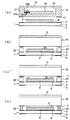
図1(a)及び(b)は本発明の一実施形態に係る表面実装型圧電発振器の斜視図、及び正面図である。図2は実装基板母材上に圧電振動子個片を搭載する状態を示す斜視図である。
この圧電発振器は、絶縁基板2の底部に表面実装用の実装電極5を4個備えると共に、絶縁基板2の平坦な上面に4個の接合電極4とランド6を備えた実装基板1と、発振回路、温度補償回路等を構成する電子部品として実装基板1のランド6上にフリップチップ等によって実装されるIC部品3と、実装基板1の上面に形成した4個の接合電極4と個別に半田接合される4個の底部電極11を下面に備えた圧電振動子10と、を2階建て構造で接合一体化した構成を備えている。
圧電振動子10は、図3(a)に示すように、セラミック容器(絶縁容器)12の上面に形成した凹所13内に水晶振動素子等の圧電振動素子14を収容すると共に、凹所13を金属蓋15にて気密封止した構成を備えている。凹所13内の段差上には2つの内部パッド13aを配置し、この内部パッド13a上に導電性接着剤によって圧電振動素子14を片持ち支持する。各内部パッド13aは、夫々圧電振動素子上の励振電極と導通している。また、各内部パッド13aは、内部導体13bを介して対応する底部電極11と導通している。
このセラミック容器12及び金属蓋15からなるパッケージは、例えば3.2×2.5mmサイズを使用することができ、従ってこのパッケージ内には、f=15MHz以下の周波数帯の発振周波数を有した圧電振動素子を収容可能である。
IC部品3は、例えばワンチップICであり、その底部にはランド6と接続される電極を有すると共に、上面3Aは電極を有しない平坦面となっている。
実装基板1の接合電極4と、圧電振動子10の底部電極11とは、導電性接合材20を用いて電気的機械的に接合一体化されている。導電性接合材20としては、例えば半田等のろう材、又は導電性ペースト等を用いる。従って、本実施形態では、柱部材、金属ブロック等の格別の専用部品を用いていない。
本発明の圧電発振器の他の特徴的な構成は、IC部品3の上面3Aによって圧電振動子10の底面を直接、又は間接的に、機械的に支持した点にある。
なお、ICチップ3の上面3Aと圧電振動子10の下面との間に、シリコン樹脂等から成る緩衝材21を介在させて、ICチップ3の上面とセラミック容器底面との直接の接触を防止するようにしてもよい(図3(c))。このように緩衝材21を介在させることにより、IC部品上に圧電振動子を搭載した際に、IC部品にセラミック容器が直接接触することによって、IC部品がパッケージからの押圧力を強く受けて、圧電発振器の電気的特性が不安定化する虞を回避することができる。
緩衝材21は、IC部品上面3Aの外周縁に沿って線状、環状に配置しても良いし、点状に複数箇所配置しても良い。前者の場合には、集積回路が配置されているIC部品の中央部を回避した位置に圧電振動子からの圧力伝達経路となる緩衝材21が配置されるので、集積回路への衝撃が伝達されにくくなる。このような問題がない場合には、IC部品の上面中央部に緩衝材を配置してもよい。何れにしても緩衝剤21によって、IC部品3に対して衝撃が伝達される経路が限定されるので、集積回路などの要保護部位に対する圧力等による衝撃を効果的に緩和することができる。
Hereinafter, the present invention will be described in detail with reference to embodiments shown in the drawings.
1A and 1B are a perspective view and a front view of a surface mount piezoelectric oscillator according to an embodiment of the present invention. FIG. 2 is a perspective view showing a state where the piezoelectric vibrator pieces are mounted on the mounting substrate base material.
The piezoelectric oscillator includes four
As shown in FIG. 3A, the
The package made of the
The
The
Another characteristic configuration of the piezoelectric oscillator of the present invention is that the bottom surface of the
Note that a
The
本発明の圧電発振器を製造する場合には、まず、複数のセラミック容器12をシート状に連結した構造のセラミック容器母材と、複数の実装基板1をシート状に連結した構造の実装基板母材を、夫々焼成により製造する。各セラミック容器母材は、これを個片に分割してから各凹所13内に対して圧電振動素子14を搭載し、その後金属蓋15による気密封止を行うこととなる。
次いで、実装基板母材1A上の実装基板個片領域上に形成したランド6上にIC部品3をフリップチップ実装し、更に実装基板個片領域上の接合電極4上に各セラミック容器の底部電極11を一対一で対応させつつ、導電性接合材20を介して圧電振動子10を載置する(図2)。
実装基板母材1Aは、実装基板個片が縦横に隣接して接続配置された構成を備えており、4個の実装基板個片が隣接し合う部分には、各実装基板個片の角隅部に配置された接合電極4が集結して配置されている。従って、導電性接合材20を接合電極4に塗布するに際しては、この接合電極が集結した部分に導電性接合材20を一括して塗布してから各実装基板個片上に圧電振動子10を搭載する。その後、導電性接合材が半田の場合には一括してリフローによって半田を硬化させ、導電性接合材が導電性ペーストの場合は加熱硬化させる。最後に、破線で示した切断ラインに沿って、実装基板母材1Aを個片に切断分割して発振器個片を得る。
When manufacturing the piezoelectric oscillator of the present invention, first, a ceramic container base material having a structure in which a plurality of
Next, the
The mounting
図3(a)乃至(c)は上記製造手順を説明する工程図であり、実装基板個片上に圧電振動子個片を搭載する工程を図示説明する。
まず、図3(a)においては、実装基板1のランド6上にIC部品3をフリップチップ等によって実装する。なお、図示の例では、フリップチップのためのバンプは図示省略されている。
次いで、図3(b)において、実装基板1の接合電極4上に導電性接合材20を所要量、所要厚にて配置する。この導電性接合材20はスクリーン印刷等によって塗布することができる。なお、圧電振動子の底部電極11の面上に導電性接合材20を塗布してもよい。
なお、図3(b)のようにIC部品3上に直接圧電振動子10を載置してもよいが、図3(b)’に示すように、必要に応じてIC部品の上面適所に、予めシリコン樹脂等の緩衝材21を固着させておいてもよい。
次いで、図3(c)、図2に示すように電子部品3を覆うように圧電振動子10を実装基板1の上面に位置決め載置する。この際、各導電性接合材20を、圧電振動子10の底部電極11と位置合わせし、その後、導電性接合材20を加熱溶融等によって硬化させることにより、実装基板1に対する圧電振動子10の電気的機械的固定を完了する。
その後、実装基板母材を個片に分割した後に、圧電発振器個片の電気的特性を所定値にするために、IC部品内の回路設定を調整する。この際、IC調整用端子を実装基板個片の底面に露出配置しておくことにより、調整作業を容易化することができる。
このように本発明に係る圧電発振器によれば、格別の柱部材を用いないので、部品点数の増大によるコストアップ、組立手数の増大によるコストアップを解消できる。実装基板1に対する圧電振動子10の支持安定性は、IC部品3と圧電振動子10とを直接、又は間接的に接触させることによって確保できる。また、IC部品3と圧電振動子10との接触部には、必要に応じて接着剤を介在させてもよい。
FIGS. 3A to 3C are process diagrams for explaining the manufacturing procedure described above, and illustrate the process of mounting the piezoelectric vibrator piece on the mounting board piece.
First, in FIG. 3A, the
Next, in FIG. 3B, the
Note that the
Next, as shown in FIGS. 3C and 2, the
Thereafter, after the mounting substrate base material is divided into pieces, the circuit settings in the IC component are adjusted in order to set the electrical characteristics of the piezoelectric oscillator pieces to a predetermined value. At this time, the adjustment work can be facilitated by exposing the IC adjustment terminal to the bottom surface of the mounting board piece.
As described above, according to the piezoelectric oscillator according to the present invention, since no special column member is used, the cost increase due to the increase in the number of parts and the cost increase due to the increase in the number of assembly can be solved. Support stability of the
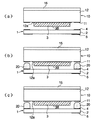
上記実施形態では、実装基板1上に搭載したIC部品3を、圧電振動子10によってサンドイッチした構成を示したが、これとは逆に圧電振動子10の底面に設けたランドにIC部品3を逆さ状態で搭載してから、実装基板上面によってIC部品3の下面3Bを支持するようにサンドイッチすることも可能である。
図4はこのような構成を備えた圧電発振器の製造手順を示す工程図である。
まず、図4(a)においては、圧電振動子10を構成する絶縁容器12下面のランド12aにIC部品3を逆さ向きにフリップチップ実装する。
次いで、図4(b)において、実装基板1の接合電極4上に導電性接合材20を所要量、所要厚にて配置する。この導電性接合材20はスクリーン印刷等によって塗布することができる。なお、より低コスト化、小型化を図る場合は、圧電振動子の底部電極11の面上に導電性接合材20を塗布してもよい。
なお、IC部品3の下面3Bを直接実装基板上面と接触させてもよいが、図3(b)’に示した例と同様に、必要に応じてIC部品の下面適所、或いは実装基板上面適所に、シリコン樹脂等の緩衝材を固着させておいてもよい。緩衝材の塗布位置等については、上記実施形態について述べたことがそのまま当てはまる。
図5は実装基板の上面に緩衝材を配置する例を示す拡大図であり、この例では実装基板1上に設けたレジスト膜25を緩衝材として利用している。この場合、レジスト膜25の下に配線パターン8を一部配線することで、レジスト膜から成る緩衝材の高さを稼ぐことができる。
次いで、図4(c)に示すように電子部品3が実装基板1によって覆われるように実装基板1を圧電振動子の下面に位置決めする。この際、各導電性接合材20を、圧電振動子10の底部電極11と位置あわせし、その後、導電性接合材20を加熱溶融等によって硬化させることにより、実装基板1に対する圧電振動子10の電気的機械的固定を完了する。
その後、実装基板母材を個片に分割した後に、圧電発振器個片の電気的特性を所定値にするために、IC部品内の回路設定を調整する。この際、IC調整用端子を実装基板個片の底面に露出配置しておくことにより、調整作業を容易化することができる。
本実施形態においても、格別の柱部材を用いないので、部品点数の増大によるコストアップ、組立手数の増大によるコストアップを解消できる。
In the above embodiment, the configuration in which the
FIG. 4 is a process diagram showing a manufacturing procedure of a piezoelectric oscillator having such a configuration.
First, in FIG. 4A, the
Next, in FIG. 4B, the
Note that the lower surface 3B of the
FIG. 5 is an enlarged view showing an example in which a buffer material is arranged on the upper surface of the mounting substrate. In this example, the resist film 25 provided on the mounting
Next, the mounting
Thereafter, after the mounting substrate base material is divided into pieces, the circuit settings in the IC component are adjusted in order to set the electrical characteristics of the piezoelectric oscillator pieces to a predetermined value. At this time, the adjustment work can be facilitated by exposing the IC adjustment terminal to the bottom surface of the mounting board piece.
Also in this embodiment, since no special column member is used, the cost increase due to the increase in the number of parts and the cost increase due to the increase in the number of assembly can be solved.
次に、図6(a)は本発明の他の実施形態に係る圧電発振器の構成を示す斜視図、(b)は分解斜視図、(c)は組立状態を示す正面図、(d)は変形例の正面図である。
この実施形態に係る圧電発振器は、実装基板1上面中央部に設けたランド6にIC部品3を搭載するとともに、実装基板の3つの角隅部に配置した接合電極4と圧電振動子1の底面の3つの底部電極11を夫々金属ブロック等からなる導電性接合材30によって電気的機械的に接合している。
本実施形態の特徴的な構成は、IC部品3の上面と圧電振動子10の底面とを接触させ、必要に応じて接着剤によって接合するようにした点にある。つまり、この実施形態では、IC部品3を、圧電振動子10を支持する手段として利用している。
なお、より低コスト化・小型化を図る場合は、金属ブロック等からなる導電性接合材30に代えて、図1に示した半田、導電性ペーストなどから成る導電性接合材20を用いても良い。
なお、ワンチップIC等のIC部品の場合、圧電振動子底面に対して接着剤によって強固に固定すると、IC部品が押圧力を受けて、発振器全体の電気特性を不安定化させることがある。このような虞を回避するためには、IC部品3と圧電振動子底面とを単に接触させるだけとするか、図6(d)のように緩衝材21を介して支持するように構成する。
なお、緩衝材21は、シリコン樹脂をIC部品上面に滴下することにより形成したり、或いはIC部品の下面側にアンダーフィル材を滴下する際に、IC部品の上面縁部に部分的にアンダーフィル材が塗布されるようにして形成してもよい。
この実施形態によれば、4個の柱部材を使用していた従来例に比して、柱部材の個数を削減できるので、低価格化と小型化を実現できる。
Next, FIG. 6A is a perspective view showing a configuration of a piezoelectric oscillator according to another embodiment of the present invention, FIG. 6B is an exploded perspective view, FIG. 6C is a front view showing an assembled state, and FIG. It is a front view of a modification.
In the piezoelectric oscillator according to this embodiment, the
The characteristic configuration of this embodiment is that the upper surface of the
In order to further reduce the cost and size, the
In the case of an IC component such as a one-chip IC, if it is firmly fixed to the bottom surface of the piezoelectric vibrator with an adhesive, the IC component may receive a pressing force and destabilize the electrical characteristics of the entire oscillator. In order to avoid such a possibility, the
The
According to this embodiment, since the number of column members can be reduced as compared with the conventional example in which four column members are used, it is possible to realize a reduction in price and size.
なお、図6に示した圧電発振器において、IC部品の上面に圧電振動子底面のGND電極(GND端子)が対面した構成とすることにより、GND端子がICチップと圧電振動子との間に介在するシールド層として機能するので、圧電振動子の動作が安定するという効果を得ることができる。更に、図6に示した圧電発振器において、実装基板1の実装電極5のうちGND端子上にIC部品を配置すれば、GND端子がIC部品に対しシールド材として機能するという効果を得ることができる。
なお、図6の実施形態において、導電性接合材30を実装基板上に予め一体化された構成としても差し支えない。
本発明は、水晶発振器のみならず、水晶以外の圧電振動子を使用した圧電発振器一般に適用することができる。
In the piezoelectric oscillator shown in FIG. 6, the GND electrode (GND terminal) on the bottom surface of the piezoelectric vibrator faces the top surface of the IC component, so that the GND terminal is interposed between the IC chip and the piezoelectric vibrator. Therefore, an effect that the operation of the piezoelectric vibrator is stabilized can be obtained. Furthermore, in the piezoelectric oscillator shown in FIG. 6, if an IC component is disposed on the GND terminal of the mounting
In the embodiment shown in FIG. 6, the
The present invention can be applied not only to a crystal oscillator but also to a general piezoelectric oscillator using a piezoelectric vibrator other than a crystal.
1 実装基板、2 絶縁基板、3 IC部品、4 接合電極、5 実装電極、6 ランド、10 圧電振動子、11 底部電極、12 セラミック容器(絶縁容器)、13 凹所、14 圧電振動素子、15 金属蓋、20 導電性接合材、21 緩衝材、25 レジスト膜、30 導電性接合材。
DESCRIPTION OF
Claims (14)
前記電子部品の上面によって前記圧電振動子の絶縁容器外底部を支持したことを特徴とする圧電発振器。 A piezoelectric vibrator having a bottom electrode which is electrically connected to the piezoelectric vibrating element in the insulating container outer bottom accommodates the piezoelectric vibrating element in the insulating vessel, a mounting board having a land and a bonding electrode on the upper surface of the insulating substrate, And an electronic component for an oscillation circuit mounted on a land of the mounting substrate, the piezoelectric vibrator is disposed above the electronic component, and a bonding electrode of the mounting substrate is disposed on a bottom electrode of the piezoelectric vibrator. A piezoelectric oscillator that is electrically and mechanically bonded using a conductive bonding material,
A piezoelectric oscillator characterized in that an outer bottom portion of an insulating container of the piezoelectric vibrator is supported by an upper surface of the electronic component.
前記実装基板の上面によって、前記電子部品の下面を支持したことを特徴とする圧電発振器。 A piezoelectric vibrator having a bottom electrode and a land that is electrically connected to the piezoelectric vibrating element in the insulating container outer bottom accommodates the piezoelectric vibrating element in the insulating vessel, a mounting substrate having a bonding electrode on the upper surface of the insulating substrate, And an electronic component for an oscillation circuit mounted on the land of the insulating container, and electrically and mechanically bonding the bonding electrode of the mounting substrate to the bottom electrode of the piezoelectric vibrator using a conductive bonding material A piezoelectric oscillator,
A piezoelectric oscillator comprising a lower surface of the electronic component supported by an upper surface of the mounting substrate.
Priority Applications (1)
| Application Number | Priority Date | Filing Date | Title |
|---|---|---|---|
| JP2004050383A JP4241430B2 (en) | 2004-02-25 | 2004-02-25 | Piezoelectric oscillator |
Applications Claiming Priority (1)
| Application Number | Priority Date | Filing Date | Title |
|---|---|---|---|
| JP2004050383A JP4241430B2 (en) | 2004-02-25 | 2004-02-25 | Piezoelectric oscillator |
Publications (3)
| Publication Number | Publication Date |
|---|---|
| JP2005244512A JP2005244512A (en) | 2005-09-08 |
| JP2005244512A5 JP2005244512A5 (en) | 2006-03-16 |
| JP4241430B2 true JP4241430B2 (en) | 2009-03-18 |
Family
ID=35025777
Family Applications (1)
| Application Number | Title | Priority Date | Filing Date |
|---|---|---|---|
| JP2004050383A Expired - Fee Related JP4241430B2 (en) | 2004-02-25 | 2004-02-25 | Piezoelectric oscillator |
Country Status (1)
| Country | Link |
|---|---|
| JP (1) | JP4241430B2 (en) |
Families Citing this family (1)
| Publication number | Priority date | Publication date | Assignee | Title |
|---|---|---|---|---|
| JP2007281597A (en) * | 2006-04-03 | 2007-10-25 | Epson Toyocom Corp | Piezoelectric device and its manufacturing method |
-
2004
- 2004-02-25 JP JP2004050383A patent/JP4241430B2/en not_active Expired - Fee Related
Also Published As
| Publication number | Publication date |
|---|---|
| JP2005244512A (en) | 2005-09-08 |
Similar Documents
| Publication | Publication Date | Title |
|---|---|---|
| US6762537B1 (en) | Piezoelectric device and method for manufacture thereof | |
| JP2006279872A (en) | Piezoelectric vibrator, manufacturing method therefor, and manufacturing method of piezoelectric oscillator using the piezoelectric vibrator | |
| US7791421B2 (en) | Surface-mounted piezoelectric oscillators | |
| JP2006311380A (en) | Piezoelectric vibrator and piezoelectric oscillator | |
| JP2006074736A (en) | Piezoelectric oscillator and method of manufacturing the same | |
| JP2010050778A (en) | Piezoelectric device | |
| EP1381151B1 (en) | Piezoelectric oscillator and its manufacturing method | |
| JP4241430B2 (en) | Piezoelectric oscillator | |
| JP4576741B2 (en) | Piezoelectric oscillator | |
| JP2013143607A (en) | Crystal oscillator for surface mounting | |
| JP4045807B2 (en) | Piezoelectric oscillator | |
| JP3405330B2 (en) | Piezoelectric oscillator | |
| JP2004135090A (en) | Surface mounted piezoelectric resonator | |
| JP4066770B2 (en) | Piezoelectric oscillator | |
| JP2008141413A (en) | Piezoelectric oscillator, and manufacturing method thereof | |
| JP4172774B2 (en) | Surface mount type piezoelectric oscillator | |
| JP2004147221A (en) | Piezoelectric oscillator | |
| JP2004260598A (en) | Surface mount temperature compensation crystal oscillator | |
| JPH0738334A (en) | Crystal oscillator | |
| WO2022024880A1 (en) | Piezoelectric device | |
| JP2004064651A (en) | Surface-mounted piezoelectric oscillator | |
| JP4645393B2 (en) | Surface mount type piezoelectric oscillator and electronic component unit | |
| KR100506734B1 (en) | multi-mode crystal oscillator | |
| JP5045316B2 (en) | Piezoelectric device | |
| KR100593908B1 (en) | A crystal oscillator |
Legal Events
| Date | Code | Title | Description |
|---|---|---|---|
| A521 | Written amendment |
Free format text: JAPANESE INTERMEDIATE CODE: A523 Effective date: 20060130 |
|
| A621 | Written request for application examination |
Free format text: JAPANESE INTERMEDIATE CODE: A621 Effective date: 20060130 |
|
| A977 | Report on retrieval |
Free format text: JAPANESE INTERMEDIATE CODE: A971007 Effective date: 20080312 |
|
| A131 | Notification of reasons for refusal |
Free format text: JAPANESE INTERMEDIATE CODE: A131 Effective date: 20080513 |
|
| A521 | Written amendment |
Free format text: JAPANESE INTERMEDIATE CODE: A523 Effective date: 20080704 |
|
| TRDD | Decision of grant or rejection written | ||
| A01 | Written decision to grant a patent or to grant a registration (utility model) |
Free format text: JAPANESE INTERMEDIATE CODE: A01 Effective date: 20081209 |
|
| A01 | Written decision to grant a patent or to grant a registration (utility model) |
Free format text: JAPANESE INTERMEDIATE CODE: A01 |
|
| A61 | First payment of annual fees (during grant procedure) |
Free format text: JAPANESE INTERMEDIATE CODE: A61 Effective date: 20081222 |
|
| FPAY | Renewal fee payment (event date is renewal date of database) |
Free format text: PAYMENT UNTIL: 20120109 Year of fee payment: 3 |
|
| R150 | Certificate of patent or registration of utility model |
Ref document number: 4241430 Country of ref document: JP Free format text: JAPANESE INTERMEDIATE CODE: R150 Free format text: JAPANESE INTERMEDIATE CODE: R150 |
|
| FPAY | Renewal fee payment (event date is renewal date of database) |
Free format text: PAYMENT UNTIL: 20120109 Year of fee payment: 3 |
|
| S111 | Request for change of ownership or part of ownership |
Free format text: JAPANESE INTERMEDIATE CODE: R313111 |
|
| FPAY | Renewal fee payment (event date is renewal date of database) |
Free format text: PAYMENT UNTIL: 20120109 Year of fee payment: 3 |
|
| R371 | Transfer withdrawn |
Free format text: JAPANESE INTERMEDIATE CODE: R371 |
|
| FPAY | Renewal fee payment (event date is renewal date of database) |
Free format text: PAYMENT UNTIL: 20120109 Year of fee payment: 3 |
|
| S111 | Request for change of ownership or part of ownership |
Free format text: JAPANESE INTERMEDIATE CODE: R313111 |
|
| FPAY | Renewal fee payment (event date is renewal date of database) |
Free format text: PAYMENT UNTIL: 20120109 Year of fee payment: 3 |
|
| R350 | Written notification of registration of transfer |
Free format text: JAPANESE INTERMEDIATE CODE: R350 |
|
| FPAY | Renewal fee payment (event date is renewal date of database) |
Free format text: PAYMENT UNTIL: 20120109 Year of fee payment: 3 |
|
| FPAY | Renewal fee payment (event date is renewal date of database) |
Free format text: PAYMENT UNTIL: 20130109 Year of fee payment: 4 |
|
| FPAY | Renewal fee payment (event date is renewal date of database) |
Free format text: PAYMENT UNTIL: 20130109 Year of fee payment: 4 |
|
| FPAY | Renewal fee payment (event date is renewal date of database) |
Free format text: PAYMENT UNTIL: 20140109 Year of fee payment: 5 |
|
| S531 | Written request for registration of change of domicile |
Free format text: JAPANESE INTERMEDIATE CODE: R313531 |
|
| R350 | Written notification of registration of transfer |
Free format text: JAPANESE INTERMEDIATE CODE: R350 |
|
| LAPS | Cancellation because of no payment of annual fees |