JP4240917B2 - Scanning circuit - Google Patents
Scanning circuit Download PDFInfo
- Publication number
- JP4240917B2 JP4240917B2 JP2002173077A JP2002173077A JP4240917B2 JP 4240917 B2 JP4240917 B2 JP 4240917B2 JP 2002173077 A JP2002173077 A JP 2002173077A JP 2002173077 A JP2002173077 A JP 2002173077A JP 4240917 B2 JP4240917 B2 JP 4240917B2
- Authority
- JP
- Japan
- Prior art keywords
- signal
- scanning
- flip
- vertical scanning
- input
- Prior art date
- Legal status (The legal status is an assumption and is not a legal conclusion. Google has not performed a legal analysis and makes no representation as to the accuracy of the status listed.)
- Expired - Fee Related
Links
Images


Classifications
-
- H—ELECTRICITY
- H04—ELECTRIC COMMUNICATION TECHNIQUE
- H04N—PICTORIAL COMMUNICATION, e.g. TELEVISION
- H04N25/00—Circuitry of solid-state image sensors [SSIS]; Control thereof
-
- H—ELECTRICITY
- H04—ELECTRIC COMMUNICATION TECHNIQUE
- H04N—PICTORIAL COMMUNICATION, e.g. TELEVISION
- H04N25/00—Circuitry of solid-state image sensors [SSIS]; Control thereof
- H04N25/40—Extracting pixel data from image sensors by controlling scanning circuits, e.g. by modifying the number of pixels sampled or to be sampled
- H04N25/44—Extracting pixel data from image sensors by controlling scanning circuits, e.g. by modifying the number of pixels sampled or to be sampled by partially reading an SSIS array
- H04N25/441—Extracting pixel data from image sensors by controlling scanning circuits, e.g. by modifying the number of pixels sampled or to be sampled by partially reading an SSIS array by reading contiguous pixels from selected rows or columns of the array, e.g. interlaced scanning
-
- H—ELECTRICITY
- H04—ELECTRIC COMMUNICATION TECHNIQUE
- H04N—PICTORIAL COMMUNICATION, e.g. TELEVISION
- H04N25/00—Circuitry of solid-state image sensors [SSIS]; Control thereof
- H04N25/40—Extracting pixel data from image sensors by controlling scanning circuits, e.g. by modifying the number of pixels sampled or to be sampled
- H04N25/46—Extracting pixel data from image sensors by controlling scanning circuits, e.g. by modifying the number of pixels sampled or to be sampled by combining or binning pixels
-
- H—ELECTRICITY
- H04—ELECTRIC COMMUNICATION TECHNIQUE
- H04N—PICTORIAL COMMUNICATION, e.g. TELEVISION
- H04N25/00—Circuitry of solid-state image sensors [SSIS]; Control thereof
- H04N25/70—SSIS architectures; Circuits associated therewith
- H04N25/71—Charge-coupled device [CCD] sensors; Charge-transfer registers specially adapted for CCD sensors
- H04N25/745—Circuitry for generating timing or clock signals
-
- H—ELECTRICITY
- H04—ELECTRIC COMMUNICATION TECHNIQUE
- H04N—PICTORIAL COMMUNICATION, e.g. TELEVISION
- H04N3/00—Scanning details of television systems; Combination thereof with generation of supply voltages
- H04N3/10—Scanning details of television systems; Combination thereof with generation of supply voltages by means not exclusively optical-mechanical
- H04N3/14—Scanning details of television systems; Combination thereof with generation of supply voltages by means not exclusively optical-mechanical by means of electrically scanned solid-state devices
- H04N3/15—Scanning details of television systems; Combination thereof with generation of supply voltages by means not exclusively optical-mechanical by means of electrically scanned solid-state devices for picture signal generation
- H04N3/155—Control of the image-sensor operation, e.g. image processing within the image-sensor
Description
【0001】
【発明の属する技術分野】
本発明は、走査回路に関するものであり、特に、間引き走査が可能な走査回路に関するものである。
【0002】
【従来の技術】
画像読み取り装置においては、例えば1行おきにあるいは1列おきに画素のデータを読み出すというように間引き走査を行うことによってフレームレートを向上させる場合がある。
【0003】
【発明が解決しようとする課題】
従来は、シフトレジスタの必要な段の出力のみを有効にすることによって間引き走査を実現していた。このため、間引き走査において、全ての素子を走査する場合と同じ走査レートを実現しようとすると、シフトレジスタに与える走査パルスとして全ての素子を走査する場合に比べて高い周波数のパルスが必要になるという問題があった。
【0004】
そこで、本発明は、間引き走査において、全ての素子を走査する場合よりも走査パルスの周波数を高くすることなく、全ての素子を走査する場合と同じ走査レートを実現することができるようにした走査回路を提供することを目的とする。
【0005】
【課題を解決するための手段】
上記の目的を達成するため、本発明では、複数のフリップフロップで構成されたシフトレジスタを備えており、前記シフトレジスタの各段の出力に基づいて対応する素子を走査する走査回路であって、前記各フリップフロップは走査信号を受け入れるための入力端子を備え、前記フリップフロップは間引き走査に応じた複数のグループに分類されており、走査回路はさらにグループ毎にフリップフロップの入力端子へ異なる走査信号の入力を行う複数の入力回路を有し、これら複数のグループのうち少なくとも一つのグループに属するフリップフロップの入力端子には、走査期間中に前記入力回路を介して入力端子にパルス状の走査信号とDCバイアス信号との何れかが選択的に供給される。
【0006】
この構成により、間引き走査を行わない素子に対応するグループに属するフリップフロップにはその入力端子にパルス状の走査信号を供給し、一方、間引き走査を行う素子に対応するグループに属するフリップフロップにはその入力端子にDCバイアス信号を供給してアクティブ状態とすることによって、間引き走査を行うことができる。そして、走査パルスの周波数を高めることなく、全ての素子を走査する場合と同じ走査レートで間引き走査を行うことができる。
【0011】
【発明の実施の形態】
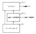
以下に本発明の実施形態を図面を参照しながら説明する。図1は本発明の走査回路を搭載した画像読み取り装置のブロック図である。図1において、10_1はX−Yアドレス型エリアセンサ、20はタイミングジェネレータ、30_1は走査モード切り替え部である。
【0012】
X−Yアドレス型エリアセンサ10_1は、そのブロック図を図2に示すように、光電変換素子を有する画素G(1、1)、G(1、2)、…、G(1、n)、G(2、1)、G(2、2)、…、G(2、n)、…、G(m、1)、G(m、2)、…、G(m、n)がマトリクス状に配置されて成るセンシング部1、センシング部1を垂直走査する垂直走査回路2_1、及び、センシング部1を水平走査する水平走査回路3_1を備えている。尚、m、nはそれぞれ正の整数である。
【0013】
センシング部1は、m本の垂直走査ラインL_1、L_2、…、L_m、n本の信号ラインS_1、S_2、…、S_n、n本の水平走査ラインC_1、C_2、…、C_n、n個のMOS型トランジスタT_1、T_2、…、T_n、及び、読み出しラインOUTを備えており、pを1≦p≦mの整数、qを1≦q≦nの整数とすると、画素G(p、q)は垂直走査ラインL_p及び信号ラインS_qに接続されている。また、各信号ラインS_qはトランジスタT_qのドレインーソース間を介して読み出しラインOUTに共通に接続されている。さらに、トランジスタT_qのゲートは水平走査ラインC_qに接続されている。
【0014】
センシング部1では、垂直走査ラインL_pがローレベルの直流電圧で駆動されると、画素G(p、1)、G(p、2)、…、G(p、n)のデータがそれぞれ信号ラインS_1、S_2、…、S_nに送出される。また、水平走査ラインC_qがローレベルの直流電圧で駆動されると、トランジスタT_qがONして信号ラインS_q上のデータが読み出しラインOUTから出力される。
【0015】
垂直走査回路2_1には、垂直走査スタート信号φVSがタイミングジェネレータ20から供給されるとともに、6種類の垂直走査信号φV1_1、φV1_2、φV1_3、φV2_1、φV2_2、φV2_3、及び、信号CNT1、CNT2、CNT3が走査モード切り替え部30_1から供給されている。
【0016】
水平走査回路3_1には、水平走査スタート信号φHSがタイミングジェネレータ20から供給されるとともに、6種類の水平走査信号φH1_1、φH1_2、φH1_3、φH2_1、φH2_2、φH2_3、及び、信号CNT1、CNT2、CNT3が走査モード切り替え部30_1から供給されている。
【0017】
垂直走査回路2_1の回路構成を図3に示す。図3において、211_1、211_2、…はフリップフロップ、212_1、212_2、…はNANDゲート、213_1、213_2、…はインバータである。尚、これらのフリップフロップ、NANDゲート、インバータをm個ずつ備えている。
【0018】
フリップフロップ211_1、211_2、…は、ストローブ信号がアクティブである間は入力がそのまま出力に素通しとなり、ストローブ信号がインアクティブになると、その直前の入力状態を保持したまま出力するタイプのラッチである。尚、このタイプのラッチはGラッチ型と呼ばれている。そして、フリップフロップ211_1、211_2、…は直列に接続されており、シフトレジスタを構成している。
【0019】
フリップフロップ211_1には垂直走査スタート信号φVSが入力されている。フリップフロップ211_2、211_3、…、211_mにはそれぞれフリップフロップ211_1、211_2、…、211_(m−1)の出力が入力されている。
【0020】
NANDゲート212_1、212_5、212_9、…の一方の入力端子には信号CNT1が入力されており、NANDゲート212_1、212_5、212_9、…の他方の入力端子にはそれぞれフリップフロップ211_1、211_5、211_9、…の出力が入力されている。
【0021】
NANDゲート212_2、212_4、212_6、…の一方の入力端子には信号CNT2が入力されており、NANDゲート212_2、212_4、212_6、…の他方の入力端子にはそれぞれフリップフロップ211_2、211_4、211_6、…の出力が入力されている。
【0022】
NANDゲート212_3、212_7、212_11、…の一方の入力端子には信号CNT3が入力されており、NANDゲート212_3、212_7、212_11、…の他方の入力端子にはそれぞれフリップフロップ211_3、211_7、211_11、…の出力が入力されている。
【0023】
NANDゲート212_pの出力はインバータ213_pに入力されている。インバータ213_pの出力によってセンシング部1の垂直走査ラインL_pが駆動される。
【0024】
各フリップフロップ211_1、211_2、…、211_mは、図4に示すように、アナログスイッチ2111、インバータ2112、アナログスイッチ2113、インバータ2114、2115、アナログスイッチ2116、インバータ2117、及び、アナログスイッチ2118を備えている。
【0025】
各フリップフロップ211_pに入力される信号はアナログスイッチ2111を介してインバータ2112に入力される。インバータ2112の出力はアナログスイッチ2113を介してインバータ2114に入力されるとともに、インバータ2115に入力される。インバータ2115の出力はアナログスイッチ2116を介してインバータ2112に入力される。インバータ2114の出力はセンシング部11の垂直走査ラインL_pを駆動するとともに、インバータ2117に入力される。インバータ2117の出力はアナログスイッチ2118を介してインバータ2114に入力される。
【0026】
フリップフロップ211_1、211_5、211_9、…では、アナログスイッチ2111は、垂直走査信号φV1_1でON/OFFが切り替えられ、垂直走査信号φV1_1がハイレベルであるときにON、垂直走査信号φV1_1がローレベルであるときにOFFとなる。
【0027】
フリップフロップ211_1、211_5、211_9、…では、アナログスイッチ2116は、垂直走査信号φV1_1の反転信号φV1_1’でON/OFFが切り替えられ、垂直走査信号φV1_1がハイレベルであるときにOFF、垂直走査信号φV1_1がローレベルであるときにONとなる。
【0028】
フリップフロップ211_1、211_5、211_9、…では、アナログスイッチ2113は、垂直走査信号φV2_1でON/OFFが切り替えられ、垂直走査信号φV2_1がハイレベルであるときにON、垂直走査信号φV2_1がローレベルであるときにOFFとなる。
【0029】
フリップフロップ211_1、211_5、211_9、…では、アナログスイッチ2118は、垂直走査信号φV2_1の反転信号φV2_1’でON/OFFが切り替えられ、垂直走査信号φV2_1がハイレベルであるときにOFF、垂直走査信号φV2_1がローレベルであるときにONとなる。
【0030】
フリップフロップ211_2、211_4、211_6、…では、アナログスイッチ2111は、垂直走査信号φV1_2でON/OFFが切り替えられ、垂直走査信号φV1_2がハイレベルであるときにON、垂直走査信号φV1_2がローレベルであるときにOFFとなる。
【0031】
フリップフロップ211_2、211_4、211_6、…では、アナログスイッチ2116は、垂直走査信号φV1_2の反転信号φV1_2’でON/OFFが切り替えられ、垂直走査信号φV1_2がハイレベルであるときにOFF、垂直走査信号φV1_2がローレベルであるときにONとなる。
【0032】
フリップフロップ211_2、211_4、211_6、…では、アナログスイッチ2113は、垂直走査信号φV2_2でON/OFFが切り替えられ、垂直走査信号φV2_2がハイレベルであるときにON、垂直走査信号φV2_2がローレベルであるときにOFFとなる。
【0033】
フリップフロップ211_2、211_4、211_6、…では、アナログスイッチ2118は、垂直走査信号φV2_2の反転信号φV2_2’でON/OFFが切り替えられ、垂直走査信号φV2_2がハイレベルであるときにOFF、垂直走査信号φV2_2がローレベルであるときにONとなる。
【0034】
フリップフロップ211_3、211_7、211_11、…では、アナログスイッチ2111は、垂直走査信号φV1_3でON/OFFが切り替えられ、垂直走査信号φV1_3がハイレベルであるときにON、垂直走査信号φV1_3がローレベルであるときにOFFとなる。
【0035】
フリップフロップ211_3、211_7、211_11、…では、アナログスイッチ2116は、垂直走査信号φV1_3の反転信号φV1_3’でON/OFFが切り替えられ、垂直走査信号φV1_3がハイレベルであるときにOFF、垂直走査信号φV1_3がローレベルであるときにONとなる。
【0036】
フリップフロップ211_3、211_7、211_11、…では、アナログスイッチ2113は、垂直走査信号φV2_3でON/OFFが切り替えられ、垂直走査信号φV2_3がハイレベルであるときにON、垂直走査信号φV2_3がローレベルであるときにOFFとなる。
【0037】
フリップフロップ211_3、211_7、211_11、…では、アナログスイッチ2118は、垂直走査信号φV2_3の反転信号φV2_3’でON/OFFが切り替えられ、垂直走査信号φV2_3がハイレベルであるときにOFF、垂直走査信号φV2_3がローレベルであるときにONとなる。
【0038】
水平走査回路3_1の回路構成は、図5に示すように、垂直走査回路2_1において垂直走査スタート信号φVS、垂直走査信号φV1_1、φV1_2、φV1_3、φV2_1、φV2_2、φV2_3をそれぞれ水平走査スタート信号φHS、水平走査信号φH1_1、φH1_2、φH1_3、φH2_1、φH2_2、φH2_3に置き換えたものである。そして、水平走査回路3_1を構成するインバータ213_qの出力によってセンシング部1の水平走査ラインC_qが駆動される。
【0039】
但し、水平走査回路3_1においては、各フリップフロップ211_1、211_2、…、211_mが、図6に示すように、垂直走査回路2_1における各フリップフロップ211_1、211_2、…、211_mの構成からインバータ2115、アナログスイッチ2116、インバータ2117、及び、アナログスイッチ2118を削除した構成となっている。これは、垂直走査信号に比して水平走査信号の周波数が高いので、インバータ2115、アナログスイッチ2116、インバータ2117、及び、アナログスイッチ2118がなくても動作上問題とならないからである。
【0040】
タイミングジェネレータ20は、図7のタイミングチャートに示す垂直走査スタート信号φVS、第1の垂直走査信号φV1、第2の垂直走査信号φV2、水平走査スタート信号φHS、第1の水平走査信号φH1、及び、第2の水平走査信号φH2を生成する。尚、図7においてVBは垂直ブランキング期間を、HBは水平ブランキング期間を、DRはデータの読み出し期間をそれぞれ表している。
【0041】
垂直走査スタート信号φVSでは、垂直ブランキング期間VBの直後の水平ブランキング期間HBに1つのパルスが立つ。第1の垂直走査信号φV1及び第2の垂直走査信号φV2では、各水平ブランキング期間HBで1つのパルスが立つ。尚、垂直走査スタート信号φVSに立つパルスはローレベルであり、また、第1の垂直走査信号φV1及び第2の垂直走査信号φV2に立つパルスはハイレベルである。
【0042】
水平走査スタート信号φHSには各水平ブランキング期間HBが終了する直前にパルスが1つ立ち、第1の水平走査信号φH1及び第2の水平走査信号φH2には所定の周期でパルスが常時発生している。水平ブランキング期間HB内で水平走査スタート信号HSにパルスが立ってから水平ブランキング期間HBの終わりまでには第1、第2の水平走査信号H1、H2にはそれぞれ1個のパルスが立っている。尚、水平走査スタート信号φHSに立つパルスはローレベルであり、また、第1の水平走査信号φH1及び第2の水平走査信号φH2に立つパルスはハイレベルである。
【0043】
走査モード切り替え部30_1の構成を図8に示す。走査モード切り替え部30_1は、セレクタ311、312、313、314、315、316、317、318、及び、制御回路319を備えている。走査モード切り替え部30_1には、タイミングジェネレータ20から出力される第1の垂直走査信号φV1、第2の垂直走査信号φV2、第1の水平走査信号φH1、及び、第2の水平走査信号φH2が入力されている。
【0044】
セレクタ311及び312は、第1の垂直走査信号φV1とハイレベルの直流電圧VDDとのうち、制御回路319から指示される方を選択して出力する。セレクタ313及び314は、第2の垂直走査信号φV2とハイレベルの直流電圧VDDとのうち、制御回路319から指示される方を選択して出力する。
【0045】
セレクタ315及び316は、第1の水平走査信号φH1とハイレベルの直流電圧VDDとのうち、制御回路319から指示される方を選択して出力する。セレクタ317及び318は、第2の水平走査信号φH2とハイレベルの直流電圧VDDとのうち、制御回路319から指示される方を選択して出力する。
【0046】
走査モード切り替え部30_1からは、第1の垂直走査信号φV1が垂直走査信号φV1_1として、セレクタ311から出力される信号がφV1_2として、セレクタ312から出力される信号がφV1_3として、第2の垂直走査信号φV2が垂直走査信号φV2_1として、セレクタ313から出力される信号がφV2_2として、セレクタ314から出力される信号がφV2_3として、それぞれ出力される。
【0047】
走査モード切り替え部30_1からは、第1の水平走査信号φH1が水平走査信号φH1_1として、セレクタ315から出力される信号がφH1_2として、セレクタ316から出力される信号がφH1_3として、第2の水平走査信号φH2が水平走査信号φH2_1として、セレクタ317から出力される信号がφH2_2として、セレクタ318から出力される信号がφH2_3として、それぞれ出力される。
【0048】
制御回路319は、走査モード指定信号によって第1の走査モードが指定されている場合には、セレクタ311及び312によって第1の垂直走査信号φV1が、セレクタ313及び314によって第2の垂直走査信号φV2が、セレクタ315及び316によって第1の水平走査信号φH1が、セレクタ317及び318によって第2の水平走査信号φH2がそれぞれ選択されるように、セレクタ311、312、313、314、315、316、317、及び、318を制御する。また、制御回路319は信号CNT1、CNT2、及び、CNT3を生成して出力しており、走査モード指定信号によって第1の走査モードが指定されている場合には、信号CNT1、CNT2、及び、CNT3をハイレベルにする。
【0049】
また、制御回路319は、走査モード指定信号によって第2の走査モードが指定されている場合には、セレクタ311によってハイレベルの直流電圧VDDが、セレクタ312によって第1の垂直走査信号φV1が、セレクタ313によってハイレベルの直流電圧VDDが、セレクタ314によって第2の垂直走査信号φV2が、セレクタ3105によってハイレベルの直流電圧VDDが、セレクタ316によって第1の水平走査信号φH1が、セレクタ317によってハイレベルの直流電圧VDDが、セレクタ318によって第2の水平走査信号φH2がそれぞれ選択されるように、セレクタ311、312、313、314、315、316、317、及び318を制御する。また、制御回路319は、走査モード指定信号によって第2の走査モードが指定されている場合には、信号CNT1をハイレベル、信号CNT2をローレベル、信号CNT3をハイレベルにする。
【0050】
さらに、制御回路319は、走査モード指定信号によって第3の走査モードが指定されている場合には、セレクタ311、312、313、314、315、316、317、及び、318によってハイレベルの直流電圧VDDが選択されるように、セレクタ311、312、313、314、315、316、317、及び318を制御する。また、制御回路319は、走査モード指定信号によって第3の走査モードが指定されている場合には、信号CNT1をハイレベル、信号CNT2及びCNT3をローレベルにする。
【0051】
以上の各部の構成により、第1の走査モードにおける垂直走査スタート信号φVS、垂直走査信号φV1_1、φV1_2、φV1_3、φV2_1、φV2_2、φV2_3のタイミングチャートは図9の(a)に示すようになり、センシング部1の全ての行の画素が1行目から順番に走査される。一方、第1の走査モードにおける水平走査スタート信号φHS、水平走査信号φH1_1、φH1_2、φH1_3、φH2_1、φH2_2、φH2_3のタイミングチャートは図10の(a)に示すようになり、センシング部1の全ての列の画素が1列目から順番に走査される。したがって、第1の走査モードでは、センシング部1の全ての画素が読み出される。
【0052】
また、第2の走査モードにおける垂直走査スタート信号φVS、垂直走査信号φV1_1、φV1_2、φV1_3、φV2_1、φV2_2、φV2_3のタイミングチャートは図9の(b)に示すようになり、センシング部1の画素が1行目の画素、3行目の画素、5行目の画素、…の順に走査される。一方、第2の走査モードにおける水平走査スタート信号φHS、水平走査信号φH1_1、φH1_2、φH1_3、φH2_1、φH2_2、φH2_3のタイミング チャートは図10の(b)に示すようになり、センシング部1の画素が1列目の画素、3列目の画素、5列目の画素、…の順に走査される。したがって、第2の走査モードでは、センシング部1の奇数行目の画素であって、且つ、奇数列目の画素である画素が読み出される。
【0053】
また、第3の走査モードにおける垂直走査スタート信号φVS、垂直走査信号φV1_1、φV1_2、φV1_3、φV2_1、φV2_2、φV2_3のタイミングチャートは図9の(c)に示すようになり、センシング部1の画素が1行目の画素、5行目の画素、9行目の画素、…の順に走査される。一方、第3の走査モードにおける水平走査スタート信号φHS、水平走査信号φH1_1、φH1_2、φH1_3、φH2_1、φH2_2、φH2_3のタイミング チャートは図10の(c)に示すようになり、センシング部1の画素が1列目の画素、5列目の画素、9列目の画素、…の順に走査される。したがって、第3の走査モードでは、センシング部1の(4x−3)行目の画素であって、且つ、(4y−3)列目の画素である画素が読み出される。尚、x、yは正の整数であ る。
【0054】
このように、第1実施形態では、間引き走査が可能となっているが、走査回路をGラッチ型のフリップフロップで構成するとともに、フリップフロップにストローブ信号(データを取り込むための信号)を与えるための配線を複数設けておき、各フリップフロップに対応するいずれか1つの配線でストローブ信号を与えるようにしているので、間引きを行わない画素に対応するフリップフロップにストローブ信号を与える配線には走査パルスを印加し、一方、間引きを行いたい画素に対応するフリップフロップにストローブ信号を与える配線には走査パルスを印加する代わりにアクティブとなる直流電圧を印加することによって間引きを行うことができ、また、間引き走査において、全ての素子を走査する場合よりも走査パルスの周波数を高くすることなく、全ての素子を走査する場合と同じ走査レートを実現することができる。
【0055】
図11は本発明の走査回路を搭載した別の画像読み取り装置のブロック図である。図11において、10_2はX−Yアドレス型エリアセンサ、20はタイミングジェネレータ、30_2は走査モード切り替え部である。尚、タイミングジェネレータ20については、上記第1実施形態のものと同一であるので、説明を省略する。
【0056】
X−Yアドレス型エリアセンサ10_2は、そのブロック図を図12に示すように、センシング部1、センシング部1を垂直走査する垂直走査回路2_2、及び、センシング部1を水平走査する水平走査回路3_2を備えている。尚、センシング部1については、上記第1実施形態のものと同一であるので、説明を省略する。
【0057】
垂直走査回路2_2には、垂直走査スタート信号φVS、第1の垂直走査信号φV1、及び、第2の垂直走査信号φV2がタイミングジェネレータ20から供給されるとともに、信号SEL_A、SEL_B、SEL_1、SEL_2、及び、SEL_3が走査モード切り替え部30_2から供給されている。
【0058】
水平走査回路3_2には、水平走査スタート信号φHS、第1の水平走査信号φH1、及び、第2の水平走査信号φH2がタイミングジェネレータ20から供給されるとともに、信号SEL_A、SEL_B、SEL_1、SEL_2、及び、SEL_3が走査モード切り替え部30_2から供給されている。
【0059】
垂直走査回路2_2の回路構成を図13に示す。図13において、221_1、221_2、…、222_1、222_2、…、223_1、223_2、…はフリップフロップ、224_1、224_2、…は4つ入力端子を備えたセレクタ、225_1、225_2、225_3は2つの入力端子を備えたセレクタである。
【0060】
フリップフロップ221_1、221_2、…は直列に接続されており、シフトレジスタを構成している。フリップフロップ222_1、222_2、…は直列に接続されており、シフトレジスタを構成している。フリップフロップ223_1、223_2、…は直列に接続されており、シフトレジスタを構成している。
【0061】
各フリップフロップ221_1、221_2、…は、Gラッチ型のフリップフロップであり、図14に示すように、アナログスイッチ2211、インバータ2212、2213、2214、アナログスイッチ2215、及び、NANDゲート2216を備えている。フリップフロップ221_1では、セレクタ225_1から出力される信号がアナログスイッチ2211を介してインバータ2212に入力されている。フリップフロップ221_1を除くフリップフロップ221_pでは、フリップフロップ221_(p−1)のインバータ2213の出力がアナログスイッチ2211を介してインバータ2212に入力されている。インバータ2212の出力はインバータ2213に入力されている。インバータ2213の出力はインバータ2214に入力されているとともに、アナログスイッチ2215を介してインバータ2212に入力されている。
【0062】
kを正の整数とすると、フリップフロップ211_(2k−1)では、アナログスイッチ2211が第1の垂直走査信号φV1で、アナログスイッチ2215が第1の垂直走査信号φV1を反転させた信号φV1’でそれぞれON/OFFが切り替えられ、第1の垂直走査信号φV1がハイレベルであるときにはアナログスイッチ2211がON、アナログスイッチ2215がOFFとなり、第1の垂直走査信号φV1がローレベルであるときにはアナログスイッチ2211がOFF、アナログスイッチ2215がONとなる。
【0063】
また、フリップフロップ211_2kでは、アナログスイッチ2211が第2の垂直走査信号φV2で、アナログスイッチ2215が第2の垂直走査信号φV2を反転させた信号φV2’でそれぞれON/OFFが切り替えられ、第2の垂直走査信号φV2がハイレベルであるときにはアナログスイッチ2211がON、アナログスイッチ2215がOFFとなり、第2の垂直走査信号φV2がローレベルであるときにはアナログスイッチ2211がOFF、アナログスイッチ2215がONとなる。
【0064】
フリップフロップ221_1では、NANDゲート2215の一方の入力端子にインバータ2214の出力が入力されており、他方の入力端子に垂直走査スタート信号φVSを反転させた信号φVSR0が入力されている。フリップフロップ221_1を除くフリップフロップ221_pでは、NANDゲート2215の一方の入力端子にインバータ2214の出力が入力されており、他方の入力端子にフリップフロップ221_(p−1)のインバータ2214の出力が入力されている。
【0065】
フリップフロップ222_1、222_2、…、及び、223_1、223_2もフリップフロップ221_1、221_2、…と同じ構成である。但し、フリップフロップ222_1では、セレクタ225_2から出力される信号がアナログスイッチ2211を介してインバータ2212に入力されている。また、フリップフロップ223_1では、セレクタ225_3から出力される信号がアナログスイッチ2211を介してインバータ2212に入力されている。
【0066】
セレクタ224_1、224_5、224_9、…、すなわち、セレクタ224_(4k−3)では、第1の入力端子にフリップフロップ221_(4k−3)のNANDゲート2216の出力が、第2の入力端子にフリップフロップ222_(2k−1)のNANDゲート2216の出力が、第3の入力端子にフリップフロップ223_kのNANDゲート2216の出力が、第4の入力端子にハイレベルの直流電圧VDDが入力されている。
【0067】
セレクタ224_2、224_4、224_6、…、すなわち、セレクタ224_2kでは、第1の入力端子にフリップフロップ221_2kのNANDゲート2216の出力が、第2の入力端子、第3の入力端子、及び、第4の入力端子にハイレベルの直流電圧VDDが入力されている。
【0068】
セレクタ224_3、224_7、224_11、…、すなわち、セレクタ224_(4k−1)では、第1の入力端子にフリップフロップ221_(4k−1)のNANDゲート2216の出力が、第2の入力端子にフリップフロップ222_2kのNANDゲート2216の出力が、第3の入力端子及び第4の入力端子にハイレベルの直流電圧VDDが入力されている。
【0069】
セレクタ224_pは信号SEL_A及びSEL_Bに基づいて4つの入力の中からいずれか1つを選択して出力する。具体的には、セレクタ224_pは、信号SEL_A、SEL_Bが共にローレベルであるときには、第1の入力端子に入力されている信号を出力し、信号SEL_Aがハイレベル、信号SEL_Bがローレベルであるときには、第2の入力端子に入力されている信号を出力し、信号SEL_Aがローレベル、信号SEL_Bがハイレベルであるときには、第3の入力端子に入力されている信号を出力し、信号SEL_A、SEL_Bが共にハイレベルであるときには、第4の入力端子に入力されている信号を出力するようになっている。そして、セレクタ224_pの出力によってセンシング部1の垂直走査ラインL_pが駆動される。
【0070】
セレクタ225_1、225_2、及び、225_3では、第1の入力端子に第1の垂直走査スタート信号φVSが、第2の入力端子にハイレベルの直流電圧VDDがそれぞれ入力されている。セレクタ225_1、225_2、225_3はそれぞれ信号SEL_1、SEL_2、SEL_3に基づいて2つの入力のうちのいずれか1つを選択して出力する。具体的には、セレクタ225_1、225_2、225_3は、それぞれ信号SEL_1、SEL_2、SEL_3がハイレベルであるときには、第1の入力端子に入力されている信号、すなわち、垂直走査スタート信号φVSを出力し、一方、それぞれ信号SEL_1、SEL_2、SEL_3がローレベルであるときには、第2の入力端子に入力されている信号、すなわち、ハイレベルの直流電圧VDDを出力する。
【0071】
水平走査回路3_2の回路構成は、図15に示すように、垂直走査回路2_2において垂直走査スタート信号φVS、第1の垂直走査信号φV1、第2の垂直走査信号φV2をそれぞれ水平走査スタート信号φHS、第1の水平走査信号φH1、第2の水平走査信号φH2に置き換えたものである。そして、水平走査回路3_2を構成するセレクタ224_qの出力によってセンシング部1の水平走査ラインC_qが駆動される。
【0072】
但し、水平走査回路3_2においては、各フリップフロップ221_1、221_2、…、222_1、222_2、…、223_1、223_2、…が、図16に示すように、垂直走査回路2_1における各フリップフロップ221_1、221_2、…、222_1、222_2、…、223_1、223_2、…の構成からアナログスイッチ2215を削除した構成となっている。これは、垂直走査信号に比して水平走査信号の周波数が高いので、アナログスイッチ2215がなくても動作上問題とならないからである。
【0073】
走査モード切り替え部30_2の構成を図17に示す。走査モード切り替え部30_2は、セレクタ321、322、323、324、325、及び、制御回路326を備えている。セレクタ321、322、323、324、及び、325は、制御回路326からの信号に基づいてハイレベルの直流電圧VDDとローレベルの直流電圧VSSとの一方を選択して出力する。
【0074】
走査モード切り替え部30_2からは、セレクタ321から出力される信号が信号SEL_Aとして、セレクタ322から出力される信号が信号SEL_Bとして、セレクタ323から出力される信号が信号SEL_1として、セレクタ324から出力される信号が信号SEL_2として、セレクタ325から出力される信号が信号SEL_3として、それぞれ出力される。
【0075】
制御回路326は、走査モード指定信号によって第1の走査モードが指定されている場合には、セレクタ321及び322によってローレベルの直流電圧VSSが、セレクタ323によってハイレベルの直流電圧VDDが、セレクタ324及び325によってローレベルの直流電圧VSSがそれぞれ選択されるように、セレクタ321、322、323、324、及び、325を制御する。
【0076】
また、制御回路326は、走査モード指定信号によって第2の走査モードが指定されている場合には、セレクタ321によってハイレベルの直流電圧VDDが、セレクタ322によってローレベルの直流電圧VSSが、セレクタ323によってローレベルの直流電圧VSSが、セレクタ324によってハイレベルの直流電圧VDDが、セレクタ325によってローレベルの直流電圧VSSがそれぞれ選択されるように、セレクタ321、322、323、324、及び、325を制御する。
【0077】
さらに、制御回路326は、走査モード指定信号によって第3の走査モードが指定されている場合には、セレクタ321によってローレベルの直流電圧VSSが、セレクタ322によってハイレベルの直流電圧VDDが、セレクタ323及び324によってローレベルの直流電圧VSSが、セレクタ325によってハイレベルの直流電圧VDDがそれぞれ選択されるように、セレクタ321、322、323、324、及び、325を制御する。
【0078】
以上の各部の構成により、第1の走査モードでは、垂直走査スタート信号φVS、第1の垂直走査信号φV1、第2の垂直走査信号φV2に対するセンシング部1の垂直走査ラインL_1、L_2、…の駆動信号のタイミングチャートは図18の(a)に示すようになり、センシング部1の全ての行の画素が1行目から順番に走査される。また、第1の走査モードでは、水平走査スタート信号φHS、第1の水平走査信号φH1、第2の水平走査信号φH2のタイミングチャートは図19の(a)に示すようになり、センシング部1の全ての列の画素が1列目から順番に走査される。したがって、第1の走査モードでは、センシング部1の全ての画素が読み出される。
【0079】
第2の走査モードでは、垂直走査スタート信号φVS、第1の垂直走査信号φV1、第2の垂直走査信号φV2に対するセンシング部1の垂直走査ラインL_1、L_2、…の駆動信号のタイミングチャートは図18の(b)に示すようになり、センシング部1の画素が1行目の画素、3行目の画素、5行目の画素、…の順に走査される。また、第2の走査モードでは、水平走査スタート信号φHS、第1の水平走査信号φH1、第2の水平走査信号φH2のタイミングチャートは図19の(b)に示すようになり、センシング部1の画素が1列目の画素、3列目の画素、5列目の画素、…の順に走査される。したがって、第2の走査モードでは、センシング部1の奇数行目の画素であって、且つ、奇数列目の画素である画素が読み出される。
【0080】
第3の走査モードでは、垂直走査スタート信号φVS、第1の垂直走査信号φV1、第2の垂直走査信号φV2に対するセンシング部1の垂直走査ラインL_1、L_2、…の駆動信号のタイミングチャートは図18の(c)に示すようになり、センシング部1の画素が1行目の画素、5行目の画素、9行目の画素、…の順に走査される。また、第3の走査モードでは、水平走査スタート信号φHS、第1の水平走査信号φH1、第2の水平走査信号φH2のタイミングチャートは図19の(c)に示すようになり、センシング部1の画素が1列目の画素、5列目の画素、9列目の画素、…の順に走査される。したがって、第3の走査モードでは、センシング部1の(4x−3)行目の画素であって、且つ、(4y−3)列目の画素である画素が読み出される。尚、x、yは正の整数である。
【0081】
このように、第2実施形態では、間引き走査が可能となっているが、段数が異なるシフトレジスタを複数設けておき、これらのいずれを用いて走査を行うかを切り替えることによって間引き走査を実現しているので、間引き走査において、全ての素子を走査する場合よりも走査パルスの周波数を高くすることなく、全ての素子を走査する場合と同じ走査レートを実現することができる。さらに、第2実施形態では、第1実施形態と比べた場合、同じ走査パルス周波数で2倍のフレームレートを実現している。別の見方をすれば、同じフレームレートを実現すればよいのであれば、第1実施形態よりも走査パルス周波数を1/2に下げることができる。
【0082】
図20は本発明の走査回路を搭載した、さらに別の画像読み取り装置のブロック図である。図20において、10_3はX−Yアドレス型エリアセンサ、20はタイミングジェネレータ、30_3は走査モード切り替え部である。尚、タイミングジェネレータ20については、上記第1実施形態のものと同一であるので、説明を省略する。
【0083】
X−Yアドレス型エリアセンサ10_3は、そのブロック図を図21に示すように、センシング部1、センシング部1を垂直走査する垂直走査回路2_3、及び、センシング部1を水平走査する水平走査回路3_3を備えている。尚、センシング部1については、上記第1実施形態のものと同一であるので、説明を省略する。
【0084】
垂直走査回路2_3には、垂直走査スタート信号φVSがタイミングジェネレータ20から供給されるとともに、4種類の垂直走査信号φV1_1、φV1_2、φV1_3、φV2_1、及び、信号SEL_1、SEL_2、SEL_3が走査モード切り替え部30_3から供給されている。
【0085】
水平走査回路3_3には、水平走査スタート信号φHSがタイミングジェネレータ20から供給されるとともに、4種類の水平走査信号φH1_1、φH1_2、φH1_3、φH2_1、及び、信号SEL_1、SEL_2、SEL_3が走査モード切り替え部30_3から供給されている。
【0086】
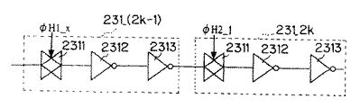
垂直走査回路2_3の回路構成を図22に示す。図22において、231_1、231_2、…はフリップフロップ、232_1、232_2、…はインバータ、233_1、233_2、…、234_1、234_2、…、235_1、235_2、…はANDゲート、236_1、236_2、…、237_1、237_2、…、238_1、238_2、…はアナログスイッチ、239_1、239_2、…はインバータである。
【0087】
フリップフロップ231_1、231_2、…はGラッチ型のフリップフロップである。そして、フリップフロップ231_1、231_2、…は直列に接続されており、シフトレジスタを構成している。
【0088】
フリップフロップ231_1には垂直走査スタート信号φVSが入力されている。フリップフロップ231_1を除くフリップフロップ231_pでは、フリップフロップ231_(p−1)の出力が入力されている。また、フリップフロップ231_pの出力はインバータ232_pに入力されている。
【0089】
ANDゲート233_1、234_1、及び、235_1では、一方の入力端子に垂直走査スタート信号φVSを反転させた信号φVSR0が入力されており、他方の入力端子にインバータ232_1の出力が入力されている。ANDゲート233_1を除くANDゲート233_pでは、一方の入力端子にインバータ232_(p−1)の出力が入力されており、他方の入力端子には、インバータ232_pの出力が入力されている。
【0090】
kを正の整数とすると、ANDゲート234_1を除くANDゲート234_(4k−3)では、一方の入力端子にインバータ232_(4k−5)の出力が入力されており、他方の入力端子にインバータ232_(4k−3)の出力が入力されている。ANDゲート235_1を除くANDゲート235_(4k−3)では、一方の入力端子にインバータ232_(4k−7)の出力が入力されており、他方の入力端子にインバータ232_(4k−3)の出力が入力されている。
【0091】
ANDゲート234_2k及び235_2kでは、一方の入力端子にローレベルの直流電圧VSSが入力されており、他方の入力端子にインバータ232_2kの出力が入力されている。
【0092】
ANDゲート234_(4k−1)では、一方の入力端子にインバータ232_(4k−3)の出力が入力されており、他方の入力端子にインバータ232_(4k−1)の出力が入力されている。ANDゲート235_(4k−1)では、一方の入力端子にローレベルの直流電圧VSSが入力されており、他方の入力端子にインバータ232_(4k−1)の出力が入力されている。
【0093】
ANDゲート233_p、234_p、235_pの出力はそれぞれアナログスイッチ236_p、237_p、238_pを介してインバータ239_pに共通に入力されている。インバータ239_pの出力によってセンシング部1の垂直走査ラインL_pが駆動される。
【0094】
アナログスイッチ236_p、237_p、238_pはそれぞれ信号SEL_1、SEL_2、SEL_3によってON/OFFが切り替えられる。具体的には、信号SEL_1、SEL_2、SEL_3がハイレベルであるときには、それぞれアナログスイッチ236_p、237_p、238_pがONとなり、一方、信号SEL_1、SEL_2、SEL_3がローレベルであるときには、それぞれアナログスイッチ236_p、237_p、238_pがOFFとなる。
【0095】
各フリップフロップ231_pは、図23に示すように、アナログスイッチ2311、インバータ2312、2313、及び、アナログスイッチ2314を備えている。各フリップフロップ231_pに入力される信号はアナログスイッチ2311を介してインバータ2312に入力される。インバータ2312の出力はインバータ2313に入力される。インバータ2313の出力はアナログスイッチ2314を介してインバータ2312に入力される。そして、インバータ2313の出力がフリップフロップ231_pの出力となる。
【0096】
フリップフロップ231_(8k−1)では、アナログスイッチ2311については垂直走査信号φV1_1で、アナログスイッチ2314については垂直走査信号φV1_1を反転させた信号φV1_1’でそれぞれON/OFFが切り替えられ、垂直走査信号φV1_1がハイレベルであるときにアナログスイッチ2311がON、アナログスイッチ2314がOFFとなり、垂直走査信号φV1_1がローレベルであるときには、アナログスイッチ2311がOFF、アナログスイッチ2314がONとなる。
【0097】
フリップフロップ231_(4k−1)では、アナログスイッチ2311については垂直走査信号φV1_2で、アナログスイッチ2314については垂直走査信号φV1_2を反転させた信号φV1_2’でそれぞれON/OFFが切り替えられ、垂直走査信号φV1_2がハイレベルであるときにアナログスイッチ2311がON、アナログスイッチ2314がOFFとなり、垂直走査信号φV1_2がローレベルであるときには、アナログスイッチ2311がOFF、アナログスイッチ2314がONとなる。
【0098】
フリップフロップ231_(8k−3)では、アナログスイッチ2311については垂直走査信号φV1_3で、アナログスイッチ2314については垂直走査信号φV1_3を反転させた信号φV1_3’でそれぞれON/OFFが切り替えられ、垂直走査信号φV1_3がハイレベルであるときにアナログスイッチ2311がON、アナログスイッチ2314がOFFとなり、垂直走査信号φV1_3がローレベルであるときには、アナログスイッチ2311がOFF、アナログスイッチ2314がONとなる。
【0099】
フリップフロップ231_2kでは、アナログスイッチ2311については垂直走査信号φV2_1で、アナログスイッチ2314については垂直走査信号φV2_1を反転させた信号φV2_1’でそれぞれON/OFFが切り替えられ、垂直走査信号φV2_1がハイレベルであるときにアナログスイッチ2311がON、アナログスイッチ2314がOFFとなり、垂直走査信号φV2_1がローレベルであるときには、アナログスイッチ2311がOFF、アナログスイッチ2314がONとなる。
【0100】
水平走査回路3_3の回路構成は、図24に示すように、垂直走査回路2_3において垂直走査スタート信号φVS、垂直走査信号φV1_1、φV1_2、φV1_3、φV2_1をそれぞれ水平走査スタート信号φHS、垂直走査信号φH1_1、φH1_2、φH1_3、φH2_1に置き換えたものである。そして、水平走査回路3_3を構成するインバータ239_qの出力によってセンシング部1の水平走査ラインC_qが駆動される。
【0101】
但し、水平走査回路3_3においては、各フリップフロップ231_1、231_2、…、231_mが、図25に示すように、垂直走査回路2_3における各フリップフロップ231_1、231_2、…、231_mの構成からアナログスイッチ2314を削除した構成となっている。これは、垂直走査信号に比して水平走査信号の周波数が高いので、アナログスイッチ2314がなくても動作上問題とならないからである。
【0102】
走査モード切り替え部30_3の構成を図26に示す。走査モード切り替え部30_3は、セレクタ331、332、333、334、335、336、及び、制御回路337を備えている。走査モード切り替え部30_3には、タイミングジェネレータ20から出力される第1の垂直走査信号φV1、第2の垂直走査信号φV2、第1の水平走査信号φH1、第2の水平走査信号φH2、及び、ハイレベルの直流電圧VDDが入力されている。
【0103】
セレクタ331は、第1の垂直走査信号φV1と第2の垂直走査信号φV2とハイレベルの直流電圧VDDとのうち、制御回路337から指示されるものを選択して出力する。セレクタ332は、第1の垂直走査信号φV1と第2の垂直走査信号φV2とのうち、制御回路337から指示される方を選択して出力する。セレクタ333は、第2の垂直走査信号φV2とハイレベルの直流電圧VDDとのうち、制御回路337から指示される方を選択して出力する。
【0104】
セレクタ334は、第1の水平走査信号φH1と第2の水平走査信号φH2とハイレベルの直流電圧VDDとのうち、制御回路337から指示されるものを選択して出力する。セレクタ335は、第1の水平走査信号φH1と第2の水平走査信号φH2とのうち、制御回路337から指示される方を選択して出力する。セレクタ336は、第2の水平走査信号φH2とハイレベルの直流電圧VDDとのうち、制御回路337から指示される方を選択して出力する。
【0105】
走査モード切り替え部30_3からは、第1の垂直走査信号φV1が信号φV1_1として、セレクタ331から出力される信号が信号φV1_2として、セレクタ332から出力される信号が信号φV1_3として、セレクタ333から出力される信号が信号φV2_1として、それぞれ出力される。
【0106】
走査モード切り替え部30_3からは、第1の水平走査信号φH1が信号φH1_1として、セレクタ331から出力される信号が信号φH1_2として、セレクタ332から出力される信号が信号φH1_3として、セレクタ333から出力される信号が信号φH2_1として、それぞれ出力される。
【0107】
制御回路337は、走査モード指定信号によって第1の走査モードが指定されている場合には、セレクタ331及び332によって第1の垂直走査信号φV1が、セレクタ333によって第2の垂直走査信号φV2が、セレクタ334及び335によって第1の水平走査信号φH1が、セレクタ336によって第2の水平走査信号φH2がそれぞれ選択されるように、セレクタ331、332、333、334、335、及び、336を制御する。また、制御回路319は、信号SEL_1、SEL_2、及び、SEL_3を生成して出力しており、走査モード指定信号によって第1の走査モードが指定されている場合には、信号SEL_1をハイレベル、信号SEL_2及びSEL_3をローレベルにする。
【0108】
また、制御回路337は、走査モード指定信号によって第2の走査モードが指定されている場合には、セレクタ331によって第2の垂直走査信号φV2が、セレクタ332によって第1の垂直走査信号φV1が、セレクタ333によってハイレベルの直流電圧VDDが、セレクタ334によって第2の水平走査信号φH2が、セレクタ335によって第1の水平走査信号φH1が、セレクタ336によってハイレベルの直流電圧VDDがそれぞれ選択されるように、セレクタ331、332、333、334、335、及び、336を制御する。また、制御回路337は、走査モード指定信号によって第2の走査モードが指定されている場合には、信号SEL_1をローレベル、信号SEL_2をハイレベル、信号SEL_3をローレベルにする。
【0109】
さらに、制御回路337は、走査モード指定信号によって第3の走査モードが指定されている場合には、セレクタ331によってハイレベルの直流電圧VDDが、セレクタ332によって第2の垂直走査信号φV2が、セレクタ333によってハイレベルの直流電圧VDDが、セレクタ334によってハイレベルの直流電圧VDDが、セレクタ335によって第2の水平走査信号φH2が、セレクタ336によってハイレベルの直流電圧VDDがそれぞれ選択されるように、セレクタ331、332、333、334、335、及び、336を制御する。また、制御回路337は、走査モード指定信号によって第3の走査モードが指定されている場合には、信号SEL_1及びSEL_2をローレベル、信号SEL_3をハイレベルにする。
【0110】
以上の各部の構成により、第1の走査モードにおける垂直走査スタート信号φVS、垂直走査信号φV1_1、φV1_2、φV1_3、φV2_1のタイミングチャートは図27の(a)に示すようになるとともに、信号SEL_1がハイレベル、信号SEL_2及びSEL_3がローレベルであるので、センシング部1の全ての行の画素が1行目から順番に走査される。一方、第1の走査モードにおける水平走査スタート信号φHS、水平走査信号φH1_1、φH1_2、φH1_3、φH2_1、φH2_2、φH2_3のタイミングチャートは図28の(a)に示すようになるとともに、信号SEL_1がハイレベル、信号SEL_2及びSEL_3がローレベルであるので、センシング部1の全ての列の画素が1列目から順番に走査される。したがって、第1の走査モードでは、センシング部1の全ての画素が読み出される。
【0111】
また、第2の走査モードにおける垂直走査スタート信号φVS、垂直走査信号φV1_1、φV1_2、φV1_3、φV2_1のタイミングチャートは図27の(b)に示すようになるとともに、信号SEL_1及びSEL_3がローレベル、信号SEL_2がハイレベルであるので、センシング部1の画素が1行目の画素、3行目の画素、5行目の画素、…の順に走査される。一方、第2の走査モードにおける水平走査スタート信号φHS、垂直走査信号φH1_1、φH1_2、φH1_3、φH2_1のタイミングチャートは図28の(b)に示すようになるとともに、信号SEL_1及びSEL_3がローレベル、信号SEL_2がハイレベルであるので、センシング部1の画素が1列目の画素、3列目の画素、5列目の画素、…の順に走査される。したがって、第2の走査モードでは、センシング部1の奇数行目の画素であって、且つ、奇数列目の画素である画素が読み出される。
【0112】
また、第3の走査モードにおける垂直走査スタート信号φVS、垂直走査信号φV1_1、φV1_2、φV1_3、φV2_1のタイミングチャートは図27の(c)に示すようになるとともに、信号SEL_1及びSEL_2がローレベル、信号SEL_3がハイレベルであるので、センシング部1の画素が1行目の画素、5行目の画素、9行目の画素、…の順に走査される。一方、第3の走査モードにおける水平走査スタート信号φHS、垂直走査信号φH1_1、φH1_2、φH1_3、φH2_1のタイミングチャートは図28の(c)に示すようになるとともに、信号SEL_1及びSEL_2がローレベル、信号SEL_3がハイレベルであるので、センシング部1の画素が1列目の画素、5列目の画素、9列目の画素、…の順に走査される。したがって、第3の走査モードでは、センシング部1の(4x−3)行目の画素であって、且つ、(4y−3)列目の画素である画素が読み出される。
【0113】
このように、第3実施形態では、間引き走査が可能となっているが、走査回路をGラッチ型のフリップフロップで構成するとともに、フリップフロップにストローブ信号(データを取り込むための信号)を与えるための配線を複数設けておき、各フリップフロップに対応するいずれか1つの配線でストローブ信号を与えるようにしているので、間引きを行わない画素に対応するフリップフロップにストローブ信号を与える配線には走査パルスを印加し、一方、間引きを行いたい画素に対応するフリップフロップにストローブ信号を与える配線には走査パルスを印加する代わりにアクティブとなる直流電圧を印加することによって間引きを行うことができ、また、間引き走査において、全ての素子を走査する場合よりも走査パルスの周波数を高くすることなく、全ての素子を走査する場合と同じ走査レートを実現することができる。さらに、第3実施形態では、第1実施形態と比べた場合、同じ走査パルス周波数で2倍のフレームレートを実現している。別の見方をすれば、同じフレームレートを実現すればよいのであれば、第1実施形態よりも走査パルス周波数を1/2に下げることができる。
【0114】
ここで、上記の各実施形態におけるセンシング部1の画素G(x、y)の構成について説明する。画素G(x、y)の回路構成例を図29に示す。尚、x、yは正の整数である。
【0115】
アノードがグランドGNDに接続されたフォトダイオードPDのカソードには、pチャネルのMOS型トランジスタT1のドレインが接続されている。トランジスタT1のソースには、pチャネルのMOS型トランジスタT2のゲート及びドレインとpチャネルのMOS型トランジスタT3のゲートが接続されている。トランジスタT1のゲートは信号φS1で駆動される。トランジスタT2のソースには信号φVPSが入力されている。
【0116】
トランジスタT3のソースには、pチャネルのMOS型トランジスタT4のゲート、pチャネルのMOS型トランジスタT5のソース、及び、一端に直流電圧VDDが印加されたコンデンサCの他端が接続されている。トランジスタT3のドレインはグランドGNDに接続されている。
【0117】
トランジスタT4のソースはpチャネルのMOS型トランジスタT6のドレインに接続されている。トランジスタT4のドレインはグランドGNDに接続されている。トランジスタT5のゲートは信号φRSTで駆動される。トランジスタT5のドレインには直流電圧VDDよりも低く、直流電圧VDDにほぼ等しい値の直流電圧RSBが印加されている。トランジスタT6のソースは信号ラインS_yに接続されている。トランジスタT6のゲートは垂直走査ラインL_xに接続されている。
【0118】
まず、撮像を行うときの動作について説明する。尚、全画素を読み出すモードに設定されている場合を例に挙げて説明する。信号φS1は撮像動作の間は常にローレベルであり、トランジスタT1がONの状態である。また、信号φRSTはハイレベルであり、トランジスタT5がOFFの状態である。さらに、信号φVPSがトランジスタT2がサブスレッショルド領域で動作するような低い値の直流電圧となっている。
【0119】
フォトダイオードPDには入射光量に応じた電流が発生し、MOS型トランジスタのサブスレッショルド特性により、トランジスタT2及びT3のゲートに光電流を自然対数的に変換した値の電圧が発生する。この電圧に応じた電流がコンデンサCを介してMOSトランジスタT3のドレインに流れ、コンデンサCが充電される。したがって、トランジスタT4のゲート電圧がフォトダイオードPDの入射光量の積分値に対して自然対数的に比例した電圧となる。
【0120】
そして、垂直走査ラインL_xを駆動する信号φV_xがローレベルになると、トランジスタT6がONになり、トランジスタT4がソースフォロワとして動作し、信号ラインS_yにフォトダイオードPDの入射光量の積分値に対して自然対数的に比例した電圧が現れる。
【0121】
このように、この例では、各画素が積分機能付き対数変換型の構成となっているが、積分機能がないものであっても構わないし、また、対数変換型でなくても構わない。
【0122】
次に、画素の感度ばらつきを検出するときの動作について、図30に示すタイミングチャートを用いて説明する。尚、全画素を読み出すモードに設定されている場合を例に挙げて説明する。まず、垂直走査ラインL_xを駆動する信号φV_xがローレベルになって画素値が読み出された後、信号φS1をハイレベルにしてトランジスタT1をOFFにして、リセット動作が始まる。
【0123】
このとき、トランジスタT2のソース側より正の電荷が流れ込み、トランジスタT2のゲート及びドレイン、並びに、トランジスタT3のゲートに蓄積された負の電荷が再結合され、トランジスタT2のゲート及びドレインのポテンシャルがある程度まで上昇する。
【0124】
しかし、トランジスタT2のゲート及びドレインのポテンシャルがある程度まで上昇すると、そのリセット速度が遅くなる。特に、明るい被写体が急に暗くなった場合にこの傾向が顕著となる。そこで、次に、トランジスタT2のソースに与える信号φVPSを撮像時の値よりも高い直流電圧にする。このように、トランジスタT2のソース電圧を高くすることで、トランジスタT2のソース側から流入する正の電荷の量が増加し、トランジスタT2のゲート及びドレイン、並びに、トランジスタT3のゲートに蓄積された負の電荷が速やかに再結合される。
【0125】
よって、トランジスタT2のゲート及びドレインのポテンシャルがさらに高くなる。そして、トランジスタT2のソースに与える信号φVPSを撮像時の低電圧に戻すことによって、トランジスタT2のポテンシャル状態を元の状態に戻す。このように、トランジスタT2のポテンシャル状態を元の状態にリセットした後、まず、信号φRSTにローレベルのパルスを立ててトランジスタT5をONにして、コンデンサCとトランジスタT4のゲートとの接続点の電圧を初期化する。
【0126】
そして、コンデンサCとトランジスタT4のゲートとの接続点の電圧が、リセットされたトランジスタT2のゲート電圧に応じたものとなると、垂直走査ラインL_xを駆動する信号φV_xがローレベルにしてトランジスタT6をONさせることによって、トランジスタT2、T3の特性のばらつきに起因する各画素の感度ばらつきを表す出力電流が信号ラインS_yから流れる。
【0127】
このとき、トランジスタT4がソースフォロワとして動作するため、信号ラインS_yにはノイズ信号が電圧信号として現れる。その後、再び、信号RSTにローレベルのパルスを立ててトランジスタT5をONさせて、コンデンサCとトランジスタT4のゲートとの接続点の電圧をリセットした後、信号φS1をローレベルにしてトランジスタT1をONにして撮像動作を行える状態にする。
【0128】
尚、2×2画素を1ユニットとして読み出す場合には信号φS1を後出する信号φS4に、4×4画素を1ユニットとして読み出す場合には信号φS1を後出する信号φS16それぞれに置き換えればよい。
【0129】
画素間の第1の回路構成を図31に示す。尚、図31はセンシング部1の4×4の16画素を示している。各画素G(x、y)のフォトダイオードPDのカソードにはpチャネルのMOS型トランジスタT7(x、y)のドレインが接続されている。
【0130】
トランジスタT7(2x−1、2y−1)、T7(2x−1、2y)、T7(2x、2y−1)、及び、T7(2x、2y)のソースはpチャネルのMOS型トランジスタT8(x、y)のドレインに共通に接続されている。トランジスタT7(x、y)のゲートは信号φA4で駆動される。トランジスタT8(x、y)のソースは画素G(2x−1、2y−1)のトランジスタT1とトランジスタT2との接続点に接続されている。トランジスタT8(x、y)のゲートは信号φS4で駆動される。
【0131】
また、トランジスタT7(2x−1、2y−1)、T7(2x−1、2y)、T7(2x、2y−1)、及び、T7(2x、2y)のソースはpチャネルのMOS型トランジスタT9(x、y)のドレインに共通に接続されている。トランジスタT9(2x−1、2y−1)、T9(2x−1、2y)、T9(2x、2y−1)、及び、T9(2x、2y)のソースはpチャネルのMOS型トランジスタT10(x、y)のドレインに共通に接続されている。トランジスタT9(x、y)のゲートは信号φA16で駆動される。トランジスタT10(x、y)のソースは画素G(4x−3、4y−3)のトランジスタT1とトランジスタT2との接続点に接続されている。トランジスタT10(x、y)のゲートは信号φS16で駆動される。
【0132】
そして、第1の走査モードである場合、すなわち、全画素が読み出される場合には、信号φS1として信号φPDDA(フォトダイオードPDをディスエーブル状態にする必要がある際にハイレベルとなる信号)が使用され、信号φS4、φS16、φA4、φA16はそれぞれハイレベルになる。これにより、トランジスタT7(x、y)、T8(x、y)、T9(x、y)、及び、T10(x、y)は常時OFF、トランジスタT1が読み出し時にはONとなるので、各画素G(x、y)における光電流が別個に読み出される。
【0133】
また、第2の走査モードである場合、すなわち、奇数行目の画素であって、且つ、奇数列目の画素である画素が読み出される場合には、信号φS4として信号φPDDAが使用され、信号φS1、φS16、φA16はそれぞれハイレベルになり、信号φA4はローレベルになる。これにより、トランジスタT1、T9(x、y)、及び、T10(x、y)が常時OFF、トランジスタT7(x、y)が常時ON、トランジスタT8(x、y)が読み出し時にはONとなるので、画素G(2x−1、2x−1)、G(2x−1、2x)、G(2x、2x−1)、及び、G(2x、2x)の4画素(2×2の4画素)における光電流がG(2x−1、2x−1)において加算されて読み出される。
【0134】
さらに、第3の走査モードである場合、すなわち、(4x−3)行目の画素であって、且つ、(4y−3)列目の画素である画素が読み出される場合には、信号φS16として信号φPDDAが使用され、信号φS1、φS4はそれぞれハイレベルになり、信号φA4、φA16はそれぞれローレベルになる。これにより、トランジスタT1及びT8(x、y)が常時OFF、トランジスタT7(x、y)及びT9(x、y)が常時ON、トランジスタT10(x、y)が読み出し時にはONとなるので、画素G(2w−1、2w−1)、G(2w−1、2w)、G(2w−1、2w+1)、G(2w−1、2w+2)、G(2w、2w−1)、G(2w、2w)、G(2w、2w+1)、G(2w、2w+2)、G(2w+1、2w−1)、G(2w+1、2w)、G(2w+1、2w+1)、G(2w+1、2w+2)、G(2w+2、2w−1)、G(2w+2、2w)、G(2w+2、2w+1)、及び、G(2w+2、2w+2)の16画素(4×4の16画素)における光電流がG(2w−1、2w−1)において加算されて読み出される。尚、wは奇数である。
【0135】
画素間の第2の回路構成を図32に示す。尚、図32はセンシング部1の4×4の16画素を示している。各画素G(x、y)のフォトダイオードPDのカソードにはpチャネルのMOS型トランジスタT11(x、y)のドレイン、及び、pチャネルのMOS型トランジスタT12(x、y)のドレインが接続されている。
【0136】
トランジスタT11(2x−1、2y−1)、T11(2x−1、2y)、T11(2x、2y−1)、及び、T11(2x、2y)のソースは画素G(2x−1、2y−1)のトランジスタT1とトランジスタT2との接続点に共通に接続されている。トランジスタT11(x、y)のゲートは信号φS4で駆動される。
【0137】
トランジスタT12(2w−1、2w−1)、T12(2w−1、2w)、T12(2w−1、2w+1)、T12(2w−1、2w+2)、T12(2w、2w−1)、T12(2w、2w)、T12(2w、2w+1)、T12(2w、2w+2)、T12(2w+1、2w−1)、T12(2w+1、2w)、T12(2w+1、2w+1)、T12(2w+1、2w+2)、T12(2w+2、2w−1)、T12(2w+2、2w)、T12(2w+2、2w+1)、及び、T12(2w+2、2w+2)のソースは画素G(2w−1、2w−1)のトランジスタT1とトランジスタT2との接続点に共通に接続されている。トランジスタT12(x、y)のゲートは信号φS16で駆動される。尚、wは奇数である。
【0138】
そして、第1の走査モードである場合、すなわち、全画素が読み出される場合には、信号φS1として信号φPDDA(フォトダイオードPDをディスエーブル状態にする必要がある際にハイレベルとなる信号)が使用され、信号φS4、φS16はそれぞれハイレベルになる。これにより、トランジスタT11(x、y)及びT12(x、y)は常時OFF、トランジスタT1が読み出し時にはONとなるので、各画素G(x、y)における光電流が別個に読み出される。
【0139】
また、第2の走査モードである場合、すなわち、奇数行目の画素であって、且つ、奇数列目の画素である画素が読み出される場合には、信号φS4として信号φPDDAが使用され、信号φS1、φS16はそれぞれハイレベルになる。これにより、トランジスタT1及びT12(x、y)が常時OFF、トランジスタT11(x、y)が読み出し時にはONとなるので、画素G(2x−1、2x−1)、G(2x−1、2x)、G(2x、2x−1)、及び、G(2x、2x)の4画素(2×2の4画素)における光電流がG(2x−1、2x−1)において加算されて読み出される。
【0140】
さらに、第3の走査モードである場合、すなわち、(4x−3)行目の画素であって、且つ、(4x−3)列目の画素である画素が読み出される場合には、信号φS16として信号φPDDAが使用され、信号φS1、φS4はそれぞれハイレベルになる。これにより、トランジスタT1及びT11(x、y)が常時OFF、トランジスタT12(x、y)が読み出し時にはONとなるので、画素G(2w−1、2w−1)、G(2w−1、2w)、G(2w−1、2w+1)、G(2w−1、2w+2)、G(2w、2w−1)、G(2w、2w)、G(2w、2w+1)、G(2w、2w+2)、G(2w+1、2w−1)、G(2w+1、2w)、G(2w+1、2w+1)、G(2w+1、2w+2)、G(2w+2、2w−1)、G(2w+2、2w)、G(2w+2、2w+1)、及び、G(2w+2、2w+2)の16画素(4×4の16画素)における光電流がG(2w−1、2w−1)において加算されて読み出される。尚、wは奇数である。
【0141】
画素間の第3の回路構成を図33に示す。尚、図33はセンシング部1の4×4の16画素を示している。各画素G(x、y)のフォトダイオードPDのカソードには、pチャネルのMOS型トランジスタT13(x、y)のドレイン、及び、pチャネルのMOS型トランジスタT14(x、y)のドレインが接続されている。また、各画素G(x、y)のトランジスタT1とトランジスタT2との接続点には、pチャネルのMOS型トランジスタT15(x、y)のソース、及び、pチャネルのMOS型トランジスタT16(x、y)のソースが接続されている。
【0142】
トランジスタT13(2x−1、2y−1)、T13(2x−1、2y)、T13(2x、2y−1)、及び、T13(2x、2y)のソース、トランジスタT15(2x−1、2y−1)、T15(2x−1、2y)、T15(2x、2y−1)、及び、T15(2x、2y)のドレインが共通に接続されている。トランジスタT13(x、y)のゲートは信号φS4で駆動される。トランジスタT15(2x−1、2y−1)のゲートは信号φB4で駆動される。トランジスタT15(2x−1、2y)、T15(2x、2y−1)、及び、T15(2x、2y)のゲートにはハイレベルの直流電圧VDDが印加されており、トランジスタT15(2x−1、2y)、T15(2x、2y−1)、及び、T15(2x、2y)は走査モードに関係なく常にOFFである。
【0143】
トランジスタT14(2w−1、2w−1)、T14(2w−1、2w)、T14(2w−1、2w+1)、T14(2w−1、2w+2)、T14(2w、2w−1)、T14(2w、2w)、T14(2w、2w+1)、T14(2w、2w+2)、T14(2w+1、2w−1)、T14(2w+1、2w)、T14(2w+1、2w+1)、T14(2w+1、2w+2)、T14(2w+2、2w−1)、T14(2w+2、2w)、T14(2w+2、2w+1)、及び、T14(2w+2、2w+2)のソース、トランジスタT16(2w−1、2w−1)、T16(2w−1、2w)、T16(2w−1、2w+1)、T16(2w−1、2w+2)、T16(2w、2w−1)、T16(2w、2w)、T16(2w、2w+1)、T16(2w、2w+2)、T16(2w+1、2w−1)、T16(2w+1、2w)、T16(2w+1、2w+1)、T16(2w+1、2w+2)、T16(2w+2、2w−1)、T16(2w+2、2w)、T16(2w+2、2w+1)、及び、T16(2w+2、2w+2)
のドレインが共通に接続されている。尚、wは奇数である。トランジスタT14(x、y)のゲートは信号φS16で駆動される。トランジスタT16(4x−3、4y−3)のゲートは信号φB16で駆動される。トランジスタT16(4x−3、4y−3)以外のトランジスタT16(x、y)のゲートにはハイレベルの直流電圧VDDが印加されており、トランジスタT16(4x−3、4y−3)以外のトランジスタT16(x、y)は走査モードに関係なく常にOFFである。
【0144】
そして、第1の走査モードである場合、すなわち、全画素が読み出される場合には、信号φS1として信号φPDDA(フォトダイオードPDをディスエーブル状態にする必要がある際にハイレベルとなる信号)が使用され、信号φS4、φS16、φB4、φB16はそれぞれハイレベルになる。これにより、トランジスタT13(x、y)、T14(x、y)、T15(x、y)、及び、T16(x、y)は常時OFF、トランジスタT1が読み出し時にはONとなるので、各画素G(x、y)における光電流が別個に読み出される。
【0145】
また、第2の走査モードである場合、すなわち、奇数行目の画素であって、且つ、奇数列目の画素である画素が読み出される場合には、信号φS4として信号φPDDAが使用され、信号φS1、φS16、φB16はそれぞれハイレベルになり、信号φB4はローレベルになる。これにより、トランジスタT1、T15(x、y)、及び、T16(x、y)が常時OFF、トランジスタT15(x、y)が常時ON、トランジスタT13(x、y)が読み出し時にはONとなるので、画素G(2x−1、2x−1)、G(2x−1、2x)、G(2x、2x−1)、及び、G(2x、2x)の4画素(2×2の4画素)における光電流がG(2x−1、2x−1)において加算されて読み出される。
【0146】
さらに、第3の走査モードである場合、すなわち、(4x−3)行目の画素であって、且つ、(4y−3)列目の画素である画素が読み出される場合には、信号φS16として信号φPDDAが使用され、信号φS1、φS4、φB4はそれぞれハイレベルになり、信号φB16はローレベルになる。これにより、トランジスタT1、T13(x、y)、及び、T15(x、y)が常時OFF、トランジスタT16(x、y)が常時ON、トランジスタT14(x、y)が読み出し時にはONとなるので、画素G(2w−1、2w−1)、G(2w−1、2w)、G(2w−1、2w+1)、G(2w−1、2w+2)、G(2w、2w−1)、G(2w、2w)、G(2w、2w+1)、G(2w、2w+2)、G(2w+1、2w−1)、G(2w+1、2w)、G(2w+1、2w+1)、G(2w+1、2w+2)、G(2w+2、2w−1)、G(2w+2、2w)、G(2w+2、2w+1)、及び、G(2w+2、2w+2)の16画素(4×4の16画素)における光電流がG(2w−1、2w−1)において加算されて読み出される。尚、wは奇数である。
【0147】
このように、上述した画素間の各回路構成によれば、間引き走査を行う際には、走査する画素における光電流と走査を間引く画素における光電流とを加算するようになっているので、間引き走査を行った際に感度が低下するという問題を防止することができる。
【0148】
ここで、図32、図33の各回路構成では、図31の回路構成に比べて、トランジスタの数が多くなるが、回路の対称性が向上し、実際にマスクレイアウトを作成する際に非常に簡便になるという利点がある。さらに、図33の回路構成では、画素間でのフォトダイオードの寄生容量を同一にすることができるので、全画素を読み出す場合における低照度感度のばらつきの発生を抑制することができる。
【0149】
尚、上記実施形態は画像読み取り装置における走査回路に本発明を適用した例を挙げて説明したが、本発明は画像読み取り装置だけに限らず、表示装置の走査回路など、他の走査回路にも適用可能である。
【0150】
【発明の効果】
以上説明したように、本発明によれば、間引き走査を行わない素子に対応するグループに属するフリップフロップにはその入力端子にパルス状 の走査信号を供給し、一方、間引き走査を行う素子に対応するグループに属するフリップフロップにはその入力端子にDCバイアス信号を供給してアクティブ状 態とすることによって間引きを行うことができ、また、間引き走査において、全ての素子を走査する場合よりも走査パルスの周波数を高くすることなく、全ての 素子を走査する場合と同じ走査レートを実現することができる。
【図面の簡単な説明】
【図1】 本発明の走査回路を搭載した画像読み取り装置のブロック図である。
【図2】 図1におけるX−Yアドレス型エリアセンサのブロック図である。
【図3】 図2における垂直走査回路の回路図である。
【図4】 図3におけるフリップフロップの回路図である。
【図5】 図2における水平走査回路の回路図である。
【図6】 図5におけるフリップフロップの回路図である。
【図7】 図1におけるタイミングジェネレータで生成される各信号のタイミングチャートである。
【図8】 図1における走査モード切り替え部のブロック図である。
【図9】 図2における垂直走査回路に入力される各信号のタイミングチャートである。
【図10】 図2における水平走査回路に入力される各信号のタイミングチャートである。
【図11】 本発明の走査回路を搭載した別の画像読み取り装置のブロック図である。
【図12】 図11におけるX−Yアドレス型エリアセンサのブロック図である。
【図13】 図12における垂直走査回路の回路図である。
【図14】 図13におけるフリップフロップの回路図である。
【図15】 図12における水平走査回路の回路図である。
【図16】 図15におけるフリップフロップの回路図である。
【図17】 図11における走査モード切り替え部のブロック図である。
【図18】 図12における垂直走査回路に入力される各信号のタイミングチャートである。
【図19】 図12における水平走査回路に入力される各信号のタイミングチャートである。
【図20】 本発明の走査回路を搭載したさらに別の画像読み取り装置のブロック図である。
【図21】 図20におけるX−Yアドレス型エリアセンサのブロック図である。
【図22】 図21における垂直走査回路の回路図である。
【図23】 図22におけるフリップフロップの回路図である。
【図24】 図21における水平走査回路の回路図である。
【図25】 図24におけるフリップフロップの回路図である。
【図26】 図20における走査モード切り替え部のブロック図である。
【図27】 図21における垂直走査回路に入力される各信号のタイミングチャートである。
【図28】 図21における水平走査回路に入力される各信号のタイミングチャートである。
【図29】 図2、図12、及び、図21のセンシング部を構成する画素の回路図である。
【図30】 画素の感度ばらつきを検出するときの各信号のタイミングチャートである。
【図31】 画素間の第1の回路構成を示す図である。
【図32】 画素間の第2の回路構成を示す図である。
【図33】 画素間の第3の回路構成を示す図である。
【符号の説明】
1 センシング部
2_1、2_2、2_3 垂直走査回路
3_1、3_2、3_3 水平走査回路
10_1、10_2、10_3 X−Yアドレス型エリアセンサ
20 タイミングジェネレータ
30_1、30_2、30_3 走査モード切り替え部[0001]
BACKGROUND OF THE INVENTION
The present invention relates to a scanning circuit, and more particularly to a scanning circuit capable of thinning scanning.
[0002]
[Prior art]
In an image reading apparatus, the frame rate may be improved by performing thinning scanning such as reading out pixel data every other row or every other column, for example.
[0003]
[Problems to be solved by the invention]
Conventionally, thinning-out scanning is realized by enabling only the output of a necessary stage of the shift register. For this reason, in the thinning scanning, if it is intended to realize the same scanning rate as when scanning all the elements, a pulse having a higher frequency is required as a scanning pulse to be supplied to the shift register than when scanning all the elements. There was a problem.
[0004]
Therefore, the present invention provides a scan that can achieve the same scanning rate as when scanning all the elements without increasing the frequency of the scanning pulse in the thinning scanning, compared with when scanning all the elements. An object is to provide a circuit.
[0005]
[Means for Solving the Problems]
In order to achieve the above object, the present invention includes a shift register including a plurality of flip-flops, and a scanning circuit that scans a corresponding element based on an output of each stage of the shift register, Each flip-flop has an input terminal for receiving a scanning signal, and the flip-flop According to thinning scan Divided into multiple groups, The scanning circuit further includes a plurality of input circuits for inputting different scanning signals to the input terminals of the flip-flops for each group, A flip-flop belonging to at least one of the plurality of groups Input terminal In , During the scanning period Via the input circuit Either the pulsed scanning signal or the DC bias signal is selectively supplied to the input terminal.
[0006]
With this configuration, a flip-flop belonging to a group corresponding to an element that does not perform decimation scanning is supplied with a pulsed scanning signal at its input terminal, while a flip-flop belonging to a group corresponding to an element that performs decimation scanning is supplied to Thinning scanning can be performed by supplying a DC bias signal to the input terminal to make it active. Then, thinning scanning can be performed at the same scanning rate as when all elements are scanned without increasing the frequency of the scanning pulse.
[0011]
DETAILED DESCRIPTION OF THE INVENTION
Embodiments of the present invention will be described below with reference to the drawings. FIG. 1 is a block diagram of an image reading apparatus equipped with a scanning circuit of the present invention. In FIG. 1, 10_1 is an XY address type area sensor, 20 is a timing generator, and 30_1 is a scanning mode switching unit.
[0012]
As shown in the block diagram of FIG. 2, the XY address type area sensor 10_1 includes pixels G (1, 1), G (1, 2),..., G (1, n), which have photoelectric conversion elements. G (2, 1), G (2, 2), ..., G (2, n), ..., G (m, 1), G (m, 2), ..., G (m, n) are in a matrix. Are provided with a
[0013]
The
[0014]
In the
[0015]
A vertical scanning start signal φVS is supplied from the
[0016]
A horizontal scanning start signal φHS is supplied from the
[0017]
FIG. 3 shows a circuit configuration of the vertical scanning circuit 2_1. 3, 211_1, 211_2, ... are flip-flops, 212_1, 212_2, ... are NAND gates, 213_1, 213_2, ... are inverters. Note that m flip-flops, NAND gates, and inverters are provided.
[0018]
The flip-flops 211_1, 211_2,... Are latches of the type in which the input is directly passed to the output as long as the strobe signal is active, and is output while maintaining the previous input state when the strobe signal becomes inactive. This type of latch is called a G latch type. The flip-flops 211_1, 211_2,... Are connected in series to form a shift register.
[0019]
The vertical scanning start signal φVS is input to the flip-flop 211_1. The outputs of the flip-flops 211_1, 211_2,..., 211_ (m−1) are input to the flip-flops 211_2, 211_3,.
[0020]
The signal CNT1 is input to one input terminal of the NAND gates 212_1, 212_5, 212_9,..., And flip-flops 211_1, 211_5, 211_9,... Are input to the other input terminals of the NAND gates 212_1, 212_5, 212_9,. Is output.
[0021]
A signal CNT2 is input to one input terminal of the NAND gates 212_2, 212_4, 212_6,..., And flip-flops 211_2, 211_4, 211_6,... Are input to the other input terminals of the NAND gates 212_2, 212_4, 212_6,. Is output.
[0022]
A signal CNT3 is input to one input terminal of the NAND gates 212_3, 212_7, 212_11,..., And flip-flops 211_3, 211_7, 211_11,... Are input to the other input terminals of the NAND gates 212_3, 212_7, 212_11,. Is output.
[0023]
The output of the NAND gate 212_p is input to the inverter 213_p. The vertical scanning line L_p of the
[0024]
Each of the flip-flops 211_1, 211_2,..., 211_m includes an
[0025]
A signal input to each flip-flop 211_p is input to the
[0026]
In the flip-flops 211_1, 211_5, 211_9,..., The
[0027]
In the flip-flops 211_1, 211_5, 211_9,..., The
[0028]
In the flip-flops 211_1, 211_5, 211_9,..., The
[0029]
In the flip-flops 211_1, 211_5, 211_9,..., The
[0030]
In the flip-flops 211_2, 211_4, 211_6,..., The
[0031]
In the flip-flops 211_2, 211_4, 211_6,..., The
[0032]
In the flip-flops 211_2, 211_4, 211_6,..., The
[0033]
In the flip-flops 211_2, 211_4, 211_6,..., The
[0034]
In the flip-flops 211_3, 211_7, 211_11,..., The
[0035]
In the flip-flops 211_3, 211_7, 211_11,..., The
[0036]
In the flip-flops 211_3, 211_7, 211_11,..., The
[0037]
In the flip-flops 211_3, 211_7, 211_11,..., The
[0038]
As shown in FIG. 5, the horizontal scanning circuit 3_1 has a vertical scanning start signal φVS, vertical scanning signals φV1_1, φV1_2, φV1_3, φV2_1, φV2_2, and φV2_3 in the horizontal scanning start signal φHS, as shown in FIG. Horizontal The scanning signals φH1_1, φH1_2, φH1_3, φH2_1, φH2_2, and φH2_3 are replaced. And the horizontal scanning line C_q of the
[0039]
However, in the horizontal scanning circuit 3_1, each of the flip-flops 211_1, 211_2,..., 211_m has an
[0040]
The
[0041]
In the vertical scanning start signal φVS, one pulse is set in the horizontal blanking period HB immediately after the vertical blanking period VB. In the first vertical scanning signal φV1 and the second vertical scanning signal φV2, one pulse is generated in each horizontal blanking period HB. Note that a pulse standing at the vertical scanning start signal φVS is at a low level, and a pulse standing at the first vertical scanning signal φV1 and the second vertical scanning signal φV2 is at a high level.
[0042]
The horizontal scanning start signal φHS has one pulse immediately before the end of each horizontal blanking period HB, and the first horizontal scanning signal φH1 and the second horizontal scanning signal φH2 always generate pulses at a predetermined cycle. ing. Within the horizontal blanking period HB, one pulse is set for each of the first and second horizontal scanning signals H1 and H2 from when the pulse is set for the horizontal scanning start signal HS until the end of the horizontal blanking period HB. Yes. Note that a pulse standing at the horizontal scanning start signal φHS is at a low level, and a pulse standing at the first horizontal scanning signal φH1 and the second horizontal scanning signal φH2 is at a high level.
[0043]
The configuration of the scanning mode switching unit 30_1 is shown in FIG. The scanning mode switching unit 30_1 includes
[0044]
The
[0045]
The
[0046]
From the scanning mode switching unit 30_1, the first vertical scanning signal φV1 is set as the vertical scanning signal φV1_1, the signal output from the
[0047]
From the scanning mode switching unit 30_1, the first horizontal scanning signal φH1 is set as the horizontal scanning signal φH1_1, the signal output from the
[0048]
When the first scanning mode is designated by the scanning mode designation signal, the
[0049]
In addition, when the second scanning mode is designated by the scanning mode designation signal, the
[0050]
Further, when the third scanning mode is designated by the scanning mode designation signal, the
[0051]
With the above-described configuration, the timing chart of the vertical scanning start signal φVS, vertical scanning signals φV1_1, φV1_2, φV1_3, φV2_1, φV2_2, and φV2_3 in the first scanning mode is as shown in FIG. The pixels in all rows of the
[0052]
Further, the timing chart of the vertical scanning start signal φVS, vertical scanning signals φV1_1, φV1_2, φV1_3, φV2_1, φV2_2, and φV2_3 in the second scanning mode is as shown in FIG. Scanning is performed in the order of pixels on the first row, pixels on the third row, pixels on the fifth row,. On the other hand, the horizontal scanning start signal φHS in the second scanning mode, Horizontal The timing chart of the scanning signals φH1_1, φH1_2, φH1_3, φH2_1, φH2_2, and φH2_3 is as shown in FIG. 10B. The pixels of the
[0053]
Further, the timing chart of the vertical scanning start signal φVS, vertical scanning signals φV1_1, φV1_2, φV1_3, φV2_1, φV2_2, and φV2_3 in the third scanning mode is as shown in FIG. Scanning is performed in the order of pixels on the first row, pixels on the fifth row, pixels on the ninth row,. On the other hand, the horizontal scanning start signal φHS in the third scanning mode, Horizontal The timing chart of the scanning signals φH1_1, φH1_2, φH1_3, φH2_1, φH2_2, and φH2_3 is as shown in FIG. 10C. The pixels of the
[0054]
As described above, in the first embodiment, thinning-out scanning is possible, but the scanning circuit is configured by a G latch type flip-flop, and a strobe signal (signal for capturing data) is given to the flip-flop. Since a strobe signal is provided by any one of the wirings corresponding to each flip-flop, a scanning pulse is applied to the wiring that provides the strobe signal to the flip-flop corresponding to the pixel that is not thinned out. On the other hand, thinning can be performed by applying an active DC voltage instead of applying a scanning pulse to a wiring that applies a strobe signal to a flip-flop corresponding to a pixel to be thinned, In thinning scanning, the scanning pulse frequency is higher than when scanning all elements. Without, it is possible to realize the same scan rate as when scanning all elements.
[0055]
FIG. 11 is a block diagram of another image reading apparatus equipped with the scanning circuit of the present invention. In FIG. 11, 10_2 is an XY address type area sensor, 20 is a timing generator, and 30_2 is a scanning mode switching unit. Since the
[0056]
As shown in a block diagram of the XY address type area sensor 10_2 in FIG. 12, the
[0057]
The vertical scanning circuit 2_2 is supplied with a vertical scanning start signal φVS, a first vertical scanning signal φV1, and a second vertical scanning signal φV2 from the
[0058]
The horizontal scanning circuit 3_2 is supplied with a horizontal scanning start signal φHS, a first horizontal scanning signal φH1, and a second horizontal scanning signal φH2 from the
[0059]
FIG. 13 shows a circuit configuration of the vertical scanning circuit 2_2. 13, 221_1, 221_2, ..., 222_1, 222_2, ..., 223_1, 223_2, ... are flip-flops, 224_1, 224_2, ... are selectors having four input terminals, and 225_1, 225_2, 225_3 are two input terminals. It is a selector provided with.
[0060]
The flip-flops 221_1, 221_2,... Are connected in series and constitute a shift register. The flip-flops 222_1, 222_2,... Are connected in series and constitute a shift register. The flip-flops 223_1, 223_2,... Are connected in series and constitute a shift register.
[0061]
Each of the flip-flops 221_1, 221_2,... Is a G latch type flip-flop, and includes an
[0062]
When k is a positive integer, in the flip-flop 211_ (2k−1), the
[0063]
In the flip-flop 211_2k, the
[0064]
In the flip-flop 221_1, the output of the
[0065]
The flip-flops 222_1, 222_2,... And 223_1, 223_2 also have the same configuration as the flip-flops 221_1, 221_2,. However, in the flip-flop 222_1, a signal output from the selector 225_2 is input to the
[0066]
In the selectors 224_1, 224_5, 224_9,..., That is, the selector 224_ (4k-3), the output of the
[0067]
In the selector 224_2, 224_4, 224_6,..., That is, the selector 224_2k, the output of the
[0068]
In the selectors 224_3, 224_7, 224_11,..., That is, the selector 224_ (4k−1), the output of the
[0069]
The selector 224_p selects and outputs one of the four inputs based on the signals SEL_A and SEL_B. Specifically, the selector 224_p outputs a signal input to the first input terminal when both the signals SEL_A and SEL_B are at a low level, and when the signal SEL_A is at a high level and the signal SEL_B is at a low level. When the signal input to the second input terminal is output and the signal SEL_A is at the low level and the signal SEL_B is at the high level, the signal input to the third input terminal is output and the signals SEL_A and SEL_B are output. When both are at the high level, the signal input to the fourth input terminal is output. Then, the vertical scanning line L_p of the
[0070]
In the selectors 225_1, 225_2, and 225_3, the first vertical scanning start signal φVS is input to the first input terminal, and the high-level DC voltage VDD is input to the second input terminal. The selectors 225_1, 225_2, and 225_3 select and output one of the two inputs based on the signals SEL_1, SEL_2, and SEL_3, respectively. Specifically, the selectors 225_1, 225_2, and 225_3 output the signal input to the first input terminal, that is, the vertical scanning start signal φVS, when the signals SEL_1, SEL_2, and SEL_3 are at a high level, On the other hand, when the signals SEL_1, SEL_2, and SEL_3 are at a low level, a signal input to the second input terminal, that is, a high-level DC voltage VDD is output.
[0071]
As shown in FIG. 15, the horizontal scanning circuit 3_2 has a circuit configuration in which a vertical scanning start signal φVS, a first vertical scanning signal φV1, and a second vertical scanning signal φV2 are respectively converted into a horizontal scanning start signal φHS, The first horizontal scanning signal φH1 and the second horizontal scanning signal φH2 are replaced. Then, the horizontal scanning line C_q of the
[0072]
However, in the horizontal scanning circuit 3_2, the flip-flops 221_1, 221_2, ..., 222_1, 222_2, ..., 223_1, 223_2, ... are connected to the flip-flops 221_1, 221_2, ... in the vertical scanning circuit 2_1 as shown in FIG. .., 222_1, 222_2,... 223_1, 223_2,. This is because, since the frequency of the horizontal scanning signal is higher than that of the vertical scanning signal, there is no problem in operation even if the
[0073]
The configuration of the scanning mode switching unit 30_2 is shown in FIG. The scanning mode switching unit 30_2 includes
[0074]
From the scanning mode switching unit 30_2, the signal output from the
[0075]
When the first scanning mode is designated by the scanning mode designation signal, the
[0076]
In addition, when the second scanning mode is designated by the scanning mode designation signal, the
[0077]
Further, when the third scanning mode is designated by the scanning mode designation signal, the
[0078]
With the configuration of each unit described above, in the first scanning mode, the vertical scanning lines L_1, L_2,... Of the
[0079]
In the second scanning mode, the timing chart of the driving signals of the vertical scanning lines L_1, L_2,... Of the
[0080]
In the third scanning mode, a timing chart of driving signals of the vertical scanning lines L_1, L_2,... Of the
[0081]
Thus, in the second embodiment, thinning scanning is possible, but thinning scanning is realized by providing a plurality of shift registers having different numbers of stages and switching which of these is used for scanning. Therefore, in the thinning-out scanning, the same scanning rate as in the case of scanning all the elements can be realized without increasing the frequency of the scanning pulse as compared with the case of scanning all the elements. Furthermore, in the second embodiment, the frame rate is doubled at the same scanning pulse frequency as compared with the first embodiment. From another point of view, the scanning pulse frequency can be reduced to ½ that of the first embodiment as long as the same frame rate is realized.
[0082]
FIG. 20 is a block diagram of still another image reading apparatus equipped with the scanning circuit of the present invention. In FIG. 20, 10_3 is an XY address type area sensor, 20 is a timing generator, and 30_3 is a scanning mode switching unit. Since the
[0083]
As shown in a block diagram of the XY address type area sensor 10_3 in FIG. 21, the
[0084]
A vertical scanning start signal φVS is supplied from the
[0085]
A horizontal scanning start signal φHS is supplied from the
[0086]
FIG. 22 shows a circuit configuration of the vertical scanning circuit 2_3. 22, 231_1, 231_2, ... are flip-flops, 232_1, 232_2, ... are inverters, 233_1, 233_2, ..., 234_1, 234_2, ..., 235_1, 235_2, ... are AND gates, 236_1, 236_2, ..., 237_1, 237_2, ..., 238_1, 238_2, ... are analog switches, 239_1, 239_2, ... are inverters.
[0087]
The flip-flops 231_1, 231_2,... Are G latch type flip-flops. The flip-flops 231_1, 231_2,... Are connected in series to form a shift register.
[0088]
A vertical scanning start signal φVS is input to the flip-flop 231_1. In the flip-flop 231_p excluding the flip-flop 231_1, the output of the flip-flop 231_ (p-1) is input. The output of the flip-flop 231_p is input to the inverter 232_p.
[0089]
In the AND gates 233_1, 234_1, and 235_1, the signal φVSR0 obtained by inverting the vertical scanning start signal φVS is input to one input terminal, and the output of the inverter 232_1 is input to the other input terminal. In the AND gate 233_p excluding the AND gate 233_1, the output of the inverter 232_ (p-1) is input to one input terminal, and the output of the inverter 232_p is input to the other input terminal.
[0090]
When k is a positive integer, the output of the inverter 232_ (4k-5) is input to one input terminal of the AND gate 234_ (4k-3) excluding the AND gate 234_1, and the inverter 232_ is input to the other input terminal. The output of (4k-3) is input. In the AND gate 235_ (4k-3) excluding the AND gate 235_1, the output of the inverter 232_ (4k-7) is input to one input terminal, and the output of the inverter 232_ (4k-3) is input to the other input terminal. Have been entered.
[0091]
In the AND gates 234_2k and 235_2k, the low-level DC voltage VSS is input to one input terminal, and the output of the inverter 232_2k is input to the other input terminal.
[0092]
In the AND gate 234_ (4k-1), the output of the inverter 232_ (4k-3) is input to one input terminal, and the output of the inverter 232_ (4k-1) is input to the other input terminal. In the AND gate 235_ (4k−1), the low-level DC voltage VSS is input to one input terminal, and the output of the inverter 232_ (4k−1) is input to the other input terminal.
[0093]
The outputs of the AND gates 233_p, 234_p, and 235_p are commonly input to the inverter 239_p through the analog switches 236_p, 237_p, and 238_p, respectively. The vertical scanning line L_p of the
[0094]
The analog switches 236_p, 237_p, and 238_p are switched ON / OFF by signals SEL_1, SEL_2, and SEL_3, respectively. Specifically, when the signals SEL_1, SEL_2, and SEL_3 are at a high level, the analog switches 236_p, 237_p, and 238_p are ON, respectively, while when the signals SEL_1, SEL_2, and SEL_3 are at a low level, the analog switches 236_p, 237_p and 238_p are turned OFF.
[0095]
Each flip-flop 231_p includes an
[0096]
In the flip-flop 231_ (8k−1), the
[0097]
In the flip-flop 231_ (4k−1), the
[0098]
In the flip-flop 231_ (8k-3), the
[0099]
In the flip-flop 231_2k, the
[0100]
As shown in FIG. 24, the horizontal scanning circuit 3_3 includes a vertical scanning start signal φVS, vertical scanning signals φV1_1, φV1_2, φV1_3, and φV2_1 as a horizontal scanning start signal φHS, a vertical scanning signal φH1_1, and a vertical scanning signal φH1_1, respectively. These are replaced with φH1_2, φH1_3, and φH2_1. Then, the horizontal scanning line C_q of the
[0101]
However, in the horizontal scanning circuit 3_3, the flip-flops 231_1, 231_2,..., 231_m are connected to the analog switches 2314 from the configuration of the flip-flops 231_1, 231_2,. The configuration is deleted. This is because, since the frequency of the horizontal scanning signal is higher than that of the vertical scanning signal, there is no problem in operation even if the
[0102]
The configuration of the scanning mode switching unit 30_3 is shown in FIG. The scanning mode switching unit 30_3 includes
[0103]
The
[0104]
The
[0105]
From the scanning mode switching unit 30_3, the first vertical scanning signal φV1 is output from the selector 333 as the signal φV1_1, the signal output from the
[0106]
From the scanning mode switching unit 30_3, the first horizontal scanning signal φH1 is output from the selector 333 as the signal φH1_1, the signal output from the
[0107]
When the first scanning mode is designated by the scanning mode designation signal, the
[0108]
Further, when the second scanning mode is designated by the scanning mode designation signal, the
[0109]
Further, when the third scanning mode is designated by the scanning mode designation signal, the
[0110]
With the above configuration, the timing chart of the vertical scanning start signal φVS, vertical scanning signals φV1_1, φV1_2, φV1_3, and φV2_1 in the first scanning mode is as shown in FIG. 27A, and the signal SEL_1 is high. Since the level and the signals SEL_2 and SEL_3 are at the low level, the pixels in all the rows of the
[0111]
In addition, the timing chart of the vertical scanning start signal φVS, vertical scanning signals φV1_1, φV1_2, φV1_3, and φV2_1 in the second scanning mode is as shown in FIG. 27B, and the signals SEL_1 and SEL_3 are at the low level. Since SEL_2 is at the high level, the pixels of the
[0112]
In addition, the timing chart of the vertical scanning start signal φVS, vertical scanning signals φV1_1, φV1_2, φV1_3, and φV2_1 in the third scanning mode is as shown in FIG. 27C, and the signals SEL_1 and SEL_2 are at the low level. Since SEL_3 is at the high level, the pixels of the
[0113]
As described above, in the third embodiment, thinning scanning is possible, but the scanning circuit is constituted by a G latch type flip-flop, and a strobe signal (signal for capturing data) is given to the flip-flop. Since a strobe signal is provided by any one of the wirings corresponding to each flip-flop, a scanning pulse is applied to the wiring that provides the strobe signal to the flip-flop corresponding to the pixel that is not thinned out. On the other hand, thinning can be performed by applying an active DC voltage instead of applying a scanning pulse to a wiring that applies a strobe signal to a flip-flop corresponding to a pixel to be thinned, In thinning scanning, the scanning pulse frequency is higher than when scanning all elements. Without, it is possible to realize the same scan rate as when scanning all elements. Furthermore, in the third embodiment, the frame rate is doubled at the same scanning pulse frequency as compared with the first embodiment. From another point of view, the scanning pulse frequency can be reduced to ½ that of the first embodiment as long as the same frame rate is realized.
[0114]
Here, the configuration of the pixel G (x, y) of the
[0115]
The drain of the p-channel MOS transistor T1 is connected to the cathode of the photodiode PD whose anode is connected to the ground GND. The source of the transistor T1 is connected to the gate and drain of a p-channel MOS transistor T2 and the gate of a p-channel MOS transistor T3. The gate of the transistor T1 is driven by a signal φS1. The signal φVPS is input to the source of the transistor T2.
[0116]
The source of the transistor T3 is connected to the gate of the p-channel MOS transistor T4, the source of the p-channel MOS transistor T5, and the other end of the capacitor C to which the DC voltage VDD is applied at one end. The drain of the transistor T3 is connected to the ground GND.
[0117]
The source of the transistor T4 is connected to the drain of the p-channel MOS transistor T6. The drain of the transistor T4 is connected to the ground GND. The gate of the transistor T5 is driven by the signal φRST. A DC voltage RSB lower than the DC voltage VDD and substantially equal to the DC voltage VDD is applied to the drain of the transistor T5. The source of the transistor T6 is connected to the signal line S_y. The gate of the transistor T6 is connected to the vertical scanning line L_x.
[0118]
First, an operation when imaging is described. A case where the mode for reading all pixels is set will be described as an example. The signal φS1 is always at a low level during the imaging operation, and the transistor T1 is in an ON state. Further, the signal φRST is at a high level, and the transistor T5 is in an OFF state. Further, the signal φVPS is a low DC voltage that allows the transistor T2 to operate in the subthreshold region.
[0119]
A current corresponding to the amount of incident light is generated in the photodiode PD, and due to the subthreshold characteristics of the MOS transistor, a voltage having a value obtained by natural logarithmic conversion of the photocurrent is generated at the gates of the transistors T2 and T3. A current corresponding to this voltage flows to the drain of the MOS transistor T3 via the capacitor C, and the capacitor C is charged. Therefore, the gate voltage of the transistor T4 becomes a voltage that is naturally logarithmically proportional to the integral value of the incident light amount of the photodiode PD.
[0120]
When the signal φV_x for driving the vertical scanning line L_x becomes a low level, the transistor T6 is turned on, the transistor T4 operates as a source follower, and the signal line S_y has a natural value relative to the integral value of the incident light amount of the photodiode PD. A logarithmically proportional voltage appears.
[0121]
As described above, in this example, each pixel has a logarithmic conversion type configuration with an integration function, but may have no integration function or may not have a logarithmic conversion type.
[0122]
Next, an operation for detecting pixel sensitivity variation will be described with reference to a timing chart shown in FIG. A case where the mode for reading all pixels is set will be described as an example. First, after the signal φV_x for driving the vertical scanning line L_x becomes a low level and the pixel value is read, the signal φS1 is set to a high level, the transistor T1 is turned off, and the reset operation starts.
[0123]
At this time, positive charges flow from the source side of the transistor T2, the negative charges accumulated in the gate and drain of the transistor T2 and the gate of the transistor T3 are recombined, and the potential of the gate and drain of the transistor T2 has a certain level. To rise.
[0124]
However, when the potential of the gate and drain of the transistor T2 rises to a certain extent, the reset speed becomes slow. This tendency is particularly noticeable when a bright subject suddenly becomes dark. Therefore, next, the signal φVPS given to the source of the transistor T2 is set to a DC voltage higher than the value at the time of imaging. In this way, by increasing the source voltage of the transistor T2, the amount of positive charge flowing from the source side of the transistor T2 increases, and the negative charge accumulated in the gate and drain of the transistor T2 and the gate of the transistor T3 is increased. The charges are recombined quickly.
[0125]
Therefore, the gate and drain potentials of the transistor T2 are further increased. Then, the signal φVPS given to the source of the transistor T2 is returned to the low voltage at the time of imaging to return the potential state of the transistor T2 to the original state. After resetting the potential state of the transistor T2 to the original state in this way, first, a low level pulse is set to the signal φRST to turn on the transistor T5, and the voltage at the connection point between the capacitor C and the gate of the transistor T4. Is initialized.
[0126]
When the voltage at the connection point between the capacitor C and the gate of the transistor T4 corresponds to the reset gate voltage of the transistor T2, the signal φV_x for driving the vertical scanning line L_x is set to the low level to turn on the transistor T6. As a result, an output current representing sensitivity variation of each pixel due to variation in characteristics of the transistors T2 and T3 flows from the signal line S_y.
[0127]
At this time, since the transistor T4 operates as a source follower, a noise signal appears as a voltage signal in the signal line S_y. After that, a low level pulse is set again to the signal RST to turn on the transistor T5, reset the voltage at the connection point between the capacitor C and the gate of the transistor T4, and then turn the signal φS1 to the low level to turn on the transistor T1. Thus, the imaging operation can be performed.
[0128]
When reading 2 × 2 pixels as one unit, the signal φS1 may be replaced with a signal φS4, and when reading 4 × 4 pixels as a unit, the signal φS1 may be replaced with a signal φS16.
[0129]
A first circuit configuration between pixels is shown in FIG. FIG. 31
[0130]
The sources of the transistors T7 (2x-1, 2y-1), T7 (2x-1, 2y), T7 (2x, 2y-1), and T7 (2x, 2y) are p-channel MOS transistors T8 (x , Y) are commonly connected to the drains. The gate of the transistor T7 (x, y) is driven by the signal φA4. The source of the transistor T8 (x, y) is connected to the connection point between the transistor T1 and the transistor T2 of the pixel G (2x-1, 2y-1). The gate of the transistor T8 (x, y) is driven by the signal φS4.
[0131]
The sources of the transistors T7 (2x-1, 2y-1), T7 (2x-1, 2y), T7 (2x, 2y-1), and T7 (2x, 2y) are p-channel MOS transistors T9. Commonly connected to the drains of (x, y). The sources of the transistors T9 (2x-1, 2y-1), T9 (2x-1, 2y), T9 (2x, 2y-1), and T9 (2x, 2y) are p-channel MOS transistors T10 (x , Y) are commonly connected to the drains. The gate of the transistor T9 (x, y) is driven by the signal φA16. The source of the transistor T10 (x, y) is connected to the connection point between the transistor T1 and the transistor T2 of the pixel G (4x-3, 4y-3). The gate of the transistor T10 (x, y) is driven by a signal φS16.
[0132]
In the first scanning mode, that is, when all the pixels are read out, the signal φPD1 (the signal that goes high when the photodiode PD needs to be disabled) is used as the signal φS1. Then, the signals φS4, φS16, φA4, and φA16 become high level. As a result, the transistors T7 (x, y), T8 (x, y), T9 (x, y), and T10 (x, y) are always OFF, and the transistor T1 is ON when reading out. The photocurrent at (x, y) is read out separately.
[0133]
In the second scanning mode, that is, when pixels in the odd-numbered rows and pixels in the odd-numbered columns are read, the signal φPDDA is used as the signal φS4, and the signal φS1 , ΦS16, φA16 are each at a high level, and the signal φA4 is at a low level. As a result, the transistors T1, T9 (x, y) and T10 (x, y) are always OFF, the transistor T7 (x, y) is always ON, and the transistor T8 (x, y) is ON when reading. , Pixels G (2x-1, 2x-1), G (2x-1, 2x), G (2x, 2x-1), and G (2x, 2x) 4 pixels (
[0134]
Further, in the case of the third scanning mode, that is, when the pixel in the (4x-3) th row and the pixel in the (4y-3) th column is read out, the signal φS16 is used. The signal φPDDA is used, the signals φS1 and φS4 are each at a high level, and the signals φA4 and φA16 are each at a low level. Accordingly, the transistors T1 and T8 (x, y) are always off, the transistors T7 (x, y) and T9 (x, y) are always on, and the transistor T10 (x, y) is on when reading out. G (2w-1, 2w-1), G (2w-1, 2w), G (2w-1, 2w + 1), G (2w-1, 2w + 2), G (2w, 2w-1), G (2w 2w), G (2w, 2w + 1), G (2w, 2w + 2), G (2w + 1, 2w-1), G (2w + 1, 2w), G (2w + 1, 2w + 1), G (2w + 1, 2w + 2), G ( 2w + 2, 2w-1), G (2w + 2, 2w), G (2w + 2, 2w + 1), and G (2w + 2, 2w + 2) in 16 pixels (4 × 4 16 pixels) have a photocurrent of G (2w-1, 2w-1) is added and read . W is an odd number.
[0135]
A second circuit configuration between the pixels is shown in FIG. FIG. 32
[0136]
The sources of the transistors T11 (2x-1, 2y-1), T11 (2x-1, 2y), T11 (2x, 2y-1), and T11 (2x, 2y) are pixels G (2x-1, 2y-). 1) is commonly connected to a connection point between the transistor T1 and the transistor T2. The gate of the transistor T11 (x, y) is driven by the signal φS4.
[0137]
Transistors T12 (2w-1, 2w-1), T12 (2w-1, 2w), T12 (2w-1, 2w + 1), T12 (2w-1, 2w + 2), T12 (2w, 2w-1), T12 ( 2w, 2w), T12 (2w, 2w + 1), T12 (2w, 2w + 2), T12 (2w + 1, 2w-1), T12 (2w + 1, 2w), T12 (2w + 1, 2w + 1), T12 (2w + 1, 2w + 2), T12 The sources of (2w + 2, 2w-1), T12 (2w + 2, 2w), T12 (2w + 2, 2w + 1), and T12 (2w + 2, 2w + 2) are the transistors T1 and T2 of the pixel G (2w-1, 2w-1). Are commonly connected to the connection point. The gate of the transistor T12 (x, y) is driven by the signal φS16. W is an odd number.
[0138]
In the first scanning mode, that is, when all the pixels are read out, the signal φPD1 (the signal that goes high when the photodiode PD needs to be disabled) is used as the signal φS1. Then, the signals φS4 and φS16 are each set to the high level. Thereby, the transistors T11 (x, y) and T12 (x, y) are always OFF, and the transistor T1 is ON when reading out, so that the photocurrent in each pixel G (x, y) is read out separately.
[0139]
In the second scanning mode, that is, when pixels in the odd-numbered rows and pixels in the odd-numbered columns are read, the signal φPDDA is used as the signal φS4, and the signal φS1 , ΦS16 become high level. As a result, the transistors T1 and T12 (x, y) are always OFF, and the transistor T11 (x, y) is ON when reading, so that the pixels G (2x-1, 2x-1), G (2x-1, 2x) ), G (2x, 2x-1), and G (2x, 2x) in 4 pixels (2x2 pixels) are added and read out in G (2x-1, 2x-1). .
[0140]
Further, in the case of the third scanning mode, that is, when a pixel that is a pixel in the (4x-3) th row and a pixel in the (4x-3) th column is read out, the signal φS16 is used. The signal φPDDA is used, and the signals φS1 and φS4 are each set to a high level. As a result, the transistors T1 and T11 (x, y) are always OFF, and the transistor T12 (x, y) is ON during reading, so that the pixels G (2w-1, 2w-1) and G (2w-1, 2w) ), G (2w-1, 2w + 1), G (2w-1, 2w + 2), G (2w, 2w-1), G (2w, 2w), G (2w, 2w + 1), G (2w, 2w + 2), G (2w + 1, 2w-1), G (2w + 1, 2w), G (2w + 1, 2w + 1), G (2w + 1, 2w + 2), G (2w + 2, 2w-1), G (2w + 2, 2w), G (2w + 2, 2w + 1) and G (2w + 2, 2w + 2) in 16 pixels (4 × 4 16 pixels) are added and read out in G (2w−1, 2w−1). W is an odd number.
[0141]
FIG. 33 shows a third circuit configuration between the pixels. FIG. 33
[0142]
The sources of transistors T13 (2x-1, 2y-1), T13 (2x-1, 2y), T13 (2x, 2y-1), and T13 (2x, 2y), transistor T15 (2x-1, 2y-) 1), drains of T15 (2x-1, 2y), T15 (2x, 2y-1), and T15 (2x, 2y) are connected in common. The gate of the transistor T13 (x, y) is driven by the signal φS4. The gate of the transistor T15 (2x-1, 2y-1) is driven by a signal φB4. A high level DC voltage VDD is applied to the gates of the transistors T15 (2x-1, 2y), T15 (2x, 2y-1), and T15 (2x, 2y), and the transistor T15 (2x-1, 2y), T15 (2x, 2y-1), and T15 (2x, 2y) are always OFF regardless of the scanning mode.
[0143]
Transistors T14 (2w-1, 2w-1), T14 (2w-1, 2w), T14 (2w-1, 2w + 1), T14 (2w-1, 2w + 2), T14 (2w, 2w-1), T14 ( 2w, 2w), T14 (2w, 2w + 1), T14 (2w, 2w + 2), T14 (2w + 1, 2w-1), T14 (2w + 1, 2w), T14 (2w + 1, 2w + 1), T14 (2w + 1, 2w + 2), T14 (2w + 2, 2w-1), T14 (2w + 2, 2w + 1), T14 (2w + 2, 2w + 1) and the source of T14 (2w + 2, 2w + 2), transistors T16 (2w-1, 2w-1), T16 (2w-1) 2w), T16 (2w-1, 2w + 1), T16 (2w-1, 2w + 2), T16 (2w, 2w-1), T16 (2w, 2w), T16 (2w, 2) +1), T16 (2w + 1, 2w-1), T16 (2w + 1, 2w-1), T16 (2w + 1, 2w + 1), T16 (2w + 1, 2w + 2), T16 (2w + 2, 2w-1), T16 (2w + 2, 2w), T16 (2w + 2, 2w + 1), and T16 (2w + 2, 2w + 2)
Are connected in common. W is an odd number. The gate of the transistor T14 (x, y) is driven by the signal φS16. The gate of the transistor T16 (4x-3, 4y-3) is driven by a signal φB16. The high-level DC voltage VDD is applied to the gates of the transistors T16 (x, y) other than the transistor T16 (4x-3, 4y-3), and the transistors other than the transistor T16 (4x-3, 4y-3). T16 (x, y) is always OFF regardless of the scanning mode.
[0144]
In the first scanning mode, that is, when all the pixels are read out, the signal φPD1 (the signal that goes high when the photodiode PD needs to be disabled) is used as the signal φS1. Then, the signals φS4, φS16, φB4, and φB16 become high level. As a result, the transistors T13 (x, y), T14 (x, y), T15 (x, y), and T16 (x, y) are always OFF, and the transistor T1 is ON when reading out. The photocurrent at (x, y) is read out separately.
[0145]
In the second scanning mode, that is, when pixels in the odd-numbered rows and pixels in the odd-numbered columns are read, the signal φPDDA is used as the signal φS4, and the signal φS1 , ΦS16, φB16 are at a high level, and the signal φB4 is at a low level. As a result, the transistors T1, T15 (x, y) and T16 (x, y) are always OFF, the transistor T15 (x, y) is always ON, and the transistor T13 (x, y) is ON when reading. , Pixels G (2x-1, 2x-1), G (2x-1, 2x), G (2x, 2x-1), and G (2x, 2x) 4 pixels (
[0146]
Further, in the case of the third scanning mode, that is, when the pixel in the (4x-3) th row and the pixel in the (4y-3) th column is read out, the signal φS16 is used. The signal φPDDA is used, the signals φS1, φS4, and φB4 are each at a high level, and the signal φB16 is at a low level. As a result, the transistors T1, T13 (x, y) and T15 (x, y) are always OFF, the transistor T16 (x, y) is always ON, and the transistor T14 (x, y) is ON when reading. , Pixels G (2w-1, 2w-1), G (2w-1, 2w), G (2w-1, 2w + 1), G (2w-1, 2w + 2), G (2w, 2w-1), G (2w, 2w), G (2w, 2w + 1), G (2w, 2w + 2), G (2w + 1, 2w-1), G (2w + 1, 2w), G (2w + 1, 2w + 1), G (2w + 1, 2w + 2), The photocurrent in 16 pixels (4 × 4 16 pixels) of G (2w + 2, 2w−1), G (2w + 2, 2w), G (2w + 2, 2w + 1), and G (2w + 2, 2w + 2) is G (2w− 1, 2w-1) is added and read It is issued. W is an odd number.
[0147]
As described above, according to each circuit configuration between the pixels described above, when thinning scanning is performed, the photocurrent in the pixel to be scanned and the photocurrent in the pixel from which scanning is thinned are added. It is possible to prevent a problem that the sensitivity is lowered when scanning is performed.
[0148]
Here, in each circuit configuration of FIG. 32 and FIG. 33, the number of transistors is larger than the circuit configuration of FIG. 31, but the symmetry of the circuit is improved, and it is very difficult to actually create a mask layout. There is an advantage that it becomes simple. Furthermore, in the circuit configuration of FIG. 33, the parasitic capacitance of the photodiodes between the pixels can be made the same, so that it is possible to suppress the occurrence of variations in the low illuminance sensitivity when all the pixels are read out.
[0149]
Although the above embodiment has been described with reference to an example in which the present invention is applied to a scanning circuit in an image reading device, the present invention is not limited to the image reading device, but may be applied to other scanning circuits such as a scanning circuit of a display device. Applicable.
[0150]
【The invention's effect】
As explained above, according to the present invention, ,while A flip-flop belonging to a group corresponding to an element not subjected to thinning scanning is supplied with a pulsed scanning signal to its input terminal, while a flip-flop belonging to a group corresponding to an element performing thinning scanning is supplied to its input terminal. Thinning can be performed by supplying a DC bias signal to the active state, and all elements can be thinned out without increasing the frequency of the scan pulse compared to scanning all elements. The same scanning rate as when scanning can be realized.
[Brief description of the drawings]
FIG. 1 is a block diagram of an image reading apparatus equipped with a scanning circuit of the present invention.
2 is a block diagram of an XY address type area sensor in FIG. 1. FIG.
3 is a circuit diagram of the vertical scanning circuit in FIG. 2. FIG.
4 is a circuit diagram of the flip-flop in FIG. 3;
5 is a circuit diagram of the horizontal scanning circuit in FIG. 2. FIG.
6 is a circuit diagram of the flip-flop in FIG. 5. FIG.
7 is a timing chart of each signal generated by the timing generator in FIG. 1. FIG.
FIG. 8 is a block diagram of a scanning mode switching unit in FIG.
FIG. 9 is a timing chart of signals input to the vertical scanning circuit in FIG.
10 is a timing chart of each signal input to the horizontal scanning circuit in FIG. 2. FIG.
FIG. 11 is a block diagram of another image reading apparatus equipped with the scanning circuit of the present invention.
12 is a block diagram of the XY address type area sensor in FIG. 11. FIG.
13 is a circuit diagram of the vertical scanning circuit in FIG. 12. FIG.
14 is a circuit diagram of the flip-flop in FIG.
15 is a circuit diagram of the horizontal scanning circuit in FIG. 12. FIG.
16 is a circuit diagram of the flip-flop in FIG.
17 is a block diagram of a scanning mode switching unit in FIG.
FIG. 18 is a timing chart of signals input to the vertical scanning circuit in FIG.
FIG. 19 is a timing chart of signals input to the horizontal scanning circuit in FIG.
FIG. 20 is a block diagram of still another image reading apparatus equipped with the scanning circuit of the present invention.
FIG. 21 is a block diagram of the XY address type area sensor in FIG. 20;
22 is a circuit diagram of the vertical scanning circuit in FIG. 21. FIG.
23 is a circuit diagram of the flip-flop in FIG.
24 is a circuit diagram of the horizontal scanning circuit in FIG. 21. FIG.
25 is a circuit diagram of the flip-flop in FIG. 24. FIG.
26 is a block diagram of a scanning mode switching unit in FIG.
27 is a timing chart of signals input to the vertical scanning circuit in FIG.
28 is a timing chart of signals input to the horizontal scanning circuit in FIG.
29 is a circuit diagram of a pixel constituting the sensing unit of FIGS. 2, 12, and 21. FIG.
FIG. 30 is a timing chart of each signal when detecting variation in sensitivity of pixels.
FIG. 31 is a diagram illustrating a first circuit configuration between pixels.
FIG. 32 is a diagram illustrating a second circuit configuration between pixels.
FIG. 33 is a diagram illustrating a third circuit configuration between pixels.
[Explanation of symbols]
1 Sensing part
2_1, 2_2, 2_3 vertical scanning circuit
3_1, 3_2, 3_3 horizontal scanning circuit
10_1, 10_2, 10_3 XY address type area sensor
20 Timing generator
30_1, 30_2, 30_3 Scanning mode switching unit
Claims (1)
Priority Applications (2)
| Application Number | Priority Date | Filing Date | Title |
|---|---|---|---|
| JP2002173077A JP4240917B2 (en) | 2002-06-13 | 2002-06-13 | Scanning circuit |
| US10/457,222 US20030231253A1 (en) | 2002-06-13 | 2003-06-09 | Image-sensing apparatus |
Applications Claiming Priority (1)
| Application Number | Priority Date | Filing Date | Title |
|---|---|---|---|
| JP2002173077A JP4240917B2 (en) | 2002-06-13 | 2002-06-13 | Scanning circuit |
Publications (2)
| Publication Number | Publication Date |
|---|---|
| JP2004023282A JP2004023282A (en) | 2004-01-22 |
| JP4240917B2 true JP4240917B2 (en) | 2009-03-18 |
Family
ID=29727893
Family Applications (1)
| Application Number | Title | Priority Date | Filing Date |
|---|---|---|---|
| JP2002173077A Expired - Fee Related JP4240917B2 (en) | 2002-06-13 | 2002-06-13 | Scanning circuit |
Country Status (2)
| Country | Link |
|---|---|
| US (1) | US20030231253A1 (en) |
| JP (1) | JP4240917B2 (en) |
Cited By (1)
| Publication number | Priority date | Publication date | Assignee | Title |
|---|---|---|---|---|
| WO2013015108A1 (en) | 2011-07-27 | 2013-01-31 | Ntn株式会社 | Sealed roller bearing |
Families Citing this family (7)
| Publication number | Priority date | Publication date | Assignee | Title |
|---|---|---|---|---|
| US7528872B2 (en) * | 2003-08-04 | 2009-05-05 | Olympus Corporation | Image apparatus, driving method, and camera |
| JP2005130382A (en) * | 2003-10-27 | 2005-05-19 | Matsushita Electric Ind Co Ltd | Solid state imaging device |
| JP4371797B2 (en) * | 2003-12-12 | 2009-11-25 | コニカミノルタホールディングス株式会社 | Solid-state imaging device |
| JP4026597B2 (en) * | 2004-01-19 | 2007-12-26 | セイコーエプソン株式会社 | Shift register having skip function, and display driver device, display device, and electronic device using the same |
| JP4692196B2 (en) * | 2005-10-04 | 2011-06-01 | ソニー株式会社 | Solid-state imaging device, driving method of solid-state imaging device, and imaging device |
| JP5115467B2 (en) * | 2008-12-18 | 2013-01-09 | 株式会社Jvcケンウッド | Solid-state imaging device and driving method thereof |
| JP2013098656A (en) * | 2011-10-28 | 2013-05-20 | Canon Inc | Scanning circuit, solid state imaging apparatus and camera |
Family Cites Families (6)
| Publication number | Priority date | Publication date | Assignee | Title |
|---|---|---|---|---|
| US5909247A (en) * | 1995-12-05 | 1999-06-01 | Olympus Optical Co., Ltd. | Solid-state image pickup apparatus |
| JP4229481B2 (en) * | 1996-07-31 | 2009-02-25 | オリンパス株式会社 | Imaging display system |
| GB2332585B (en) * | 1997-12-18 | 2000-09-27 | Simage Oy | Device for imaging radiation |
| US6956605B1 (en) * | 1998-08-05 | 2005-10-18 | Canon Kabushiki Kaisha | Image pickup apparatus |
| EP1014709A3 (en) * | 1998-12-24 | 2000-12-13 | Fuji Photo Film Co., Ltd. | Radiation image read-out method and apparatus |
| US7071980B2 (en) * | 2000-07-27 | 2006-07-04 | Canon Kabushiki Kaisha | Image sensing apparatus |
-
2002
- 2002-06-13 JP JP2002173077A patent/JP4240917B2/en not_active Expired - Fee Related
-
2003
- 2003-06-09 US US10/457,222 patent/US20030231253A1/en not_active Abandoned
Cited By (1)
| Publication number | Priority date | Publication date | Assignee | Title |
|---|---|---|---|---|
| WO2013015108A1 (en) | 2011-07-27 | 2013-01-31 | Ntn株式会社 | Sealed roller bearing |
Also Published As
| Publication number | Publication date |
|---|---|
| JP2004023282A (en) | 2004-01-22 |
| US20030231253A1 (en) | 2003-12-18 |
Similar Documents
| Publication | Publication Date | Title |
|---|---|---|
| US6947088B2 (en) | Image pickup apparatus having a common amplifier | |
| US5955753A (en) | Solid-state image pickup apparatus and image pickup apparatus | |
| US6369853B1 (en) | Intra-pixel frame storage element, array, and electronic shutter method suitable for electronic still camera applications | |
| JP3512152B2 (en) | Amplification type solid-state imaging device and driving method thereof | |
| JP3554224B2 (en) | Photoelectric conversion device | |
| JPH11103418A (en) | Photoelectric converting device | |
| JP2002077733A (en) | Solid-state image pickup device | |
| JP2002077737A (en) | Image sensor | |
| JPH0417509B2 (en) | ||
| JPS6161586B2 (en) | ||
| EP3439290A1 (en) | Image capturing element and image capturing device | |
| JPH0946597A (en) | Solid-state image pickup device and driving method therefor | |
| JP4240917B2 (en) | Scanning circuit | |
| US7718945B2 (en) | Solid state imaging device including photodetecting section, row selecting section for changing the electric charge accumulating time of each row, and signal processing section | |
| KR100595801B1 (en) | Solid state image pickup device, driving method therefor and camera | |
| JP3578648B2 (en) | Amplification type solid-state imaging device and driving method thereof | |
| JP2000188723A (en) | Image processor | |
| JPH09168117A (en) | Solid state image pickup element | |
| JP2006050403A (en) | Solid-state imaging device | |
| JP2001036059A (en) | Solid-stage image pickup device | |
| JP4345145B2 (en) | Solid-state imaging device | |
| JP4054624B2 (en) | Solid-state imaging device and signal readout method thereof | |
| JP6643656B2 (en) | Solid-state imaging device | |
| JP4312358B2 (en) | Image sensor | |
| JP2003333428A (en) | Photoelectric conversion device |
Legal Events
| Date | Code | Title | Description |
|---|---|---|---|
| A621 | Written request for application examination |
Free format text: JAPANESE INTERMEDIATE CODE: A621 Effective date: 20050325 |
|
| A711 | Notification of change in applicant |
Free format text: JAPANESE INTERMEDIATE CODE: A712 Effective date: 20050325 |
|
| A131 | Notification of reasons for refusal |
Free format text: JAPANESE INTERMEDIATE CODE: A131 Effective date: 20080507 |
|
| A521 | Request for written amendment filed |
Free format text: JAPANESE INTERMEDIATE CODE: A523 Effective date: 20080703 |
|
| TRDD | Decision of grant or rejection written | ||
| A01 | Written decision to grant a patent or to grant a registration (utility model) |
Free format text: JAPANESE INTERMEDIATE CODE: A01 Effective date: 20081209 |
|
| A01 | Written decision to grant a patent or to grant a registration (utility model) |
Free format text: JAPANESE INTERMEDIATE CODE: A01 |
|
| A61 | First payment of annual fees (during grant procedure) |
Free format text: JAPANESE INTERMEDIATE CODE: A61 Effective date: 20081222 |
|
| FPAY | Renewal fee payment (event date is renewal date of database) |
Free format text: PAYMENT UNTIL: 20120109 Year of fee payment: 3 |
|
| R150 | Certificate of patent or registration of utility model |
Free format text: JAPANESE INTERMEDIATE CODE: R150 |
|
| FPAY | Renewal fee payment (event date is renewal date of database) |
Free format text: PAYMENT UNTIL: 20130109 Year of fee payment: 4 |
|
| S531 | Written request for registration of change of domicile |
Free format text: JAPANESE INTERMEDIATE CODE: R313531 |
|
| S533 | Written request for registration of change of name |
Free format text: JAPANESE INTERMEDIATE CODE: R313533 |
|
| R350 | Written notification of registration of transfer |
Free format text: JAPANESE INTERMEDIATE CODE: R350 |
|
| LAPS | Cancellation because of no payment of annual fees |