JP4239508B2 - Light emitting element - Google Patents
Light emitting element Download PDFInfo
- Publication number
- JP4239508B2 JP4239508B2 JP2002225268A JP2002225268A JP4239508B2 JP 4239508 B2 JP4239508 B2 JP 4239508B2 JP 2002225268 A JP2002225268 A JP 2002225268A JP 2002225268 A JP2002225268 A JP 2002225268A JP 4239508 B2 JP4239508 B2 JP 4239508B2
- Authority
- JP
- Japan
- Prior art keywords
- electrode
- nitride semiconductor
- type nitride
- light emitting
- light
- Prior art date
- Legal status (The legal status is an assumption and is not a legal conclusion. Google has not performed a legal analysis and makes no representation as to the accuracy of the status listed.)
- Expired - Fee Related
Links
Images


Description
【0001】
【発明の属する技術分野】
本発明は、窒化物半導体(InXAlYGa1-X-YN、0≦X、0≦Y、X+Y≦1)を層構造に含む発光素子に係わり、特に発光効率を飛躍的に向上させた窒化物半導体発光素子に関する。
【0002】
【従来の技術】
窒化物半導体を層構造に含む窒化物半導体発光素子は高輝度純緑色発光LED、青色発光LEDとして、フルカラーLEDディスプレイ、交通信号灯、バックライトなど、様々な分野で広く利用されている。
【0003】
これらのLEDは、一般に、サファイアなどの基板上に、目的に応じた種々のn型窒化物半導体乃至p型窒化物半導体が積層された構造となっている。さらに、p型窒化物半導体上にはp電極が配置され、n型窒化物半導体上にはn電極が配置されている。
【0004】
【発明が解決しようとする課題】
しかしながら、省エネなどに伴い、発光出力の低下を伴わずに消費電力の低減を可能とするLEDが望まれている現在において、上記の構成では十分とは言えず、さらなる改良が求められている。
【0005】
すなわち、上記した従来のLEDは、発光領域にて発光した光が各種半導体または基板を介してLEDの上面および側面から出射される。より詳細には、発光領域から出射された光の一部は、あらゆる界面、すなわち基板と半導体との界面、半導体と半導体の界面、あるいは半導体と電極との界面で反射してしまう。そして、このような行程を複数回繰り返しても各々の部材に吸収されずに残った光が、LEDから出射される。
【0006】
ここで、LEDは、電流を均一に流すために、p型窒化物半導体の略全面にp電極を備える構成が主流であるが、光の一部が全面に設けられたp電極自体に吸収されてしまうという問題があった。これにより、発光領域からの光の一部が無駄になり、LED外部に光を効率よく取り出すことができなかった。さらにこれに伴い、LEDを長寿命化することが困難となってしまうという問題もあった。
【0007】
また一般に、Agは高反射材料であり上記のp電極に主として用いることで容易に取り出し効率を改善することが出来るが、接触抵抗を安定して低くすることは難しく、消費電力を十分低くすることが出来ない。またAgは容易にプラスイオンとなり、イオンマイグレーションを起こすことが知られており十分な信頼性に確保することが難しい。
【0008】
本発明はこのような問題を解決するために成されたものであり、特にp電極を特定の構成とすることにより、発光素子における光の取り出し効率をさらに向上させ、寿命の長い発光素子を提供することを目的とする。
【0009】
【課題を解決するための手段】
本発明の発光素子は、n型窒化物半導体とp型窒化物半導体を少なくとも有し、p型窒化物半導体の所定の一部にp電極を備える発光素子である。特に、p電極は、前記p型窒化物半導体に対して第2の部材よりも接触抵抗が低い第1の部材と、発光素子の光に対して第1の部材よりも反射率の高い第2の部材から少なくとも構成されており、
前記第1の部材は、前記p型窒化物半導体が露出した開口部を有し、前記第2の部材はAgであり、前記開口部内のみに充填されており、前記第1の部材上面に配置されていないことを特徴とする。これにより、発光素子からの光を第1の部材又は第2の部材により反射させ、発光素子の側面あるは鉛直方向から効率よく光を取り出すことができる。また、第2の部材をAgとすることで、効率の良い光反射を得ることができ、結果として発光素子の発光効率を向上させることができる。また、p電極は、Agよりも接触抵抗の低い第1の部材を有するので、実際に発光素子を駆動する際に、電流が主に第1の部材に集中する。これによりAgの移動、すなわちイオンマイグレーションを抑制し、信頼性を向上することができる。
【0010】
また、前記第1の部材は、複数の開口部を有するメッシュ形状であり、前記メッシュ形状の開口部内に前記第2の部材が充填されており、前記第2の部材は前記第1の部材に取り囲まれていることが好ましい。これにより、複数の開口部に第2の部材が充填されるので、第2の部材をより均等に配置することができる。
【0011】
また、第1の部材は、Ni、Au、Rh、Ir、Pd、から選択された少なくとも1つの元素を含むことが好ましい。これにより、オーミック接触を容易に得ることができる。
【0012】
また、n型窒化物半導体とp型窒化物半導体を少なくとも有し、前記p型窒化物半導体の所定の一部にp電極を備える発光素子において、前記p電極は、Ni、Au、Rh、Ir、Pdから選択された少なくとも1つの元素を含む構成である第1の部材と、前記発光素子の光に対して第1の部材よりも反射率の高いAgである第2の部材から少なくとも構成され、前記第1の部材は、前記p型窒化物半導体が露出した開口部を複数有するメッシュ形状であり、前記第2の部材は、前記第1の部材に取り囲まれるように前記メッシュ形状の開口部内に充填されていることを特徴とする。
さらにまた、前記n型窒化物半導体に設けられたn電極を、前記p電極と同一面側に備え、前記第1の部材と前記p型窒化物半導体との接触面積は、前記p電極の形成面側から見て、前記n電極から離れるに従って徐々に大きくすることもできる。
あるいは、前記n型窒化物半導体に設けられたn電極を、前記p電極と対向する面側に備え、前記n電極直上に位置する部位近傍における前記第1の部材と前記p型窒化物半導体との接触面積は、他の部位における前記第1の部材と前記p型窒化物半導体との接触面積よりも小さくすることもできる。
【0013】
【発明の実施の形態】
本実施の形態では、発光素子としてLED(Light Emitting Diode)を用いた例について説明する。本発明に係るLEDを構成する各半導体層としては種々の窒化物半導体を用いることができる。例えば、有機金属気相成長法(MOCVD)、ハイドライド気相成長法(HVPE)などによりInXAlYGa1-X-YN(但し、0≦X、0≦Y、X+Y≦1)からなる半導体を好適に用いることができる。また、その層構造としては、公知の層構造を用いることができる。例えば、MIS接合、PIN接合やPN接合を有したホモ構造、シングルヘテロ構造あるいはダブルへテロ構造のものが挙げられる。また、特定の層を超格子構造としたり、活性層を量子効果が生ずる薄膜に形成させた単一量子井戸構造や多重量子井戸構造とすることもできる。さらに、発光素子の所定の位置に公知の種々の蛍光体を配置させ、発光素子からの光を所望の光に変換することもできる。
【0014】
またLEDは、一般的には、特定の基板上に各半導体層を成長させて形成されるが、その際、基板に絶縁性基板を用いその絶縁性基板を最終的に取り除かない場合、通常、p電極およびn電極はいずれもLEDの同一面側に形成されることになる。この場合、フェイスアップ実装すなわち半導体側を視認側に配置し発光された光を半導体側から取り出すことも可能であるし、フェイスダウン実装すなわち基板側を視認側に配置し発光された光を基板側から取り出すことも可能である。もちろん、初めから絶縁性基板を用いず、あるいは最終的に絶縁性基板を取り除くことにより、p電極とn電極が半導体層構造を介して対向するように配置された構成とすることもできる。
【0015】
以下、本発明の実施の形態を図面に基づいて説明する。ただし、以下に示す実施の形態は、本発明の技術思想を具体化するためのLEDを例示するものであって、本発明のLEDを以下のものに特定するものではない。さらに、各図面が示す部材の大きさや位置関係などは、説明を明確にするため誇張していることがある。
(実施の形態1)
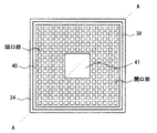
図1、2に基づいて、実施の形態1のLEDについて説明する。ここでは、図に示すように同一面側にp電極およびn電極を配置したLEDについて説明する。図1は、本実施の形態のLEDを電極形成面側から見た概略図である。また、図2は、本実施の形態のLEDの層構成を示す模式的断面図であり、図1のA−A部における断面を表す。
【0016】
図2に示すように、本実施の形態の発光素子は、例えば、サファイア基板11上にGaNバッファ層12、ノンドープGaN層13、n型コンタクト層となるSiドープGaN層14、n型クラッド層となるSiドープGaN層15、活性層となるInGaN層16、p型クラッド層となるMgドープAlGaN層17、p型コンタクト層となるMgドープGaN層18が、順次積層された層構造を有する。さらに、MgドープGaN層18、MgドープAlGaN層17、InGaN層16、SiドープGaN層15、SiドープGaN層14が部分的にエッチング等により除去され、SiドープGaN層14の露出面にn電極19が形成され、MgドープGaN層18の上面の略全面にp電極20が設けられている。なお、本実施の形態では、「特許請求の範囲」に記載するn型窒化物半導体がn型コンタクト層となるSiドープGaN層14に対応し、p型窒化物半導体がp型コンタクト層となるMgドープGaN層18に対応する。
【0017】
また、本実施の形態では、p電極20上のn電極19から離れた位置にワイヤーを接続するためのパッド部21が部分的に形成され、n電極19上及びパッド部21上の開口部を除き、各電極及び各半導体を覆うように絶縁膜(図示せず)が設けられている。なお、n電極19は、n電極自体にワイヤーを接続するためのパッド部を含む構成とする。
【0018】
ここで、p電極20は、第1の部材20aであるRhと、第2の部材20bであるAgより構成される。本実施の形態では、図1に示すように、第1の部材20aがメッシュ形状であり、かつ第2の部材20bがメッシュ形状の開口部内及び第1の部材20a上面に形成されている。メッシュ形状の第1の部材20aは、p型コンタクト層であるMgドープGaN層18の上面の略全域に渡って形成されている。必然的に、第1の部材20aの開口部に充填されている第2の部材20bも、p型コンタクト層であるMgドープGaN層18の上面の略全域に渡って形成されることになる。
【0019】
このように、第1の部材20aの開口部に第2の部材20bが充填されることにより、第2の部材20bがイオンマイグレーションし易い部材である場合に、第2の部材20bのイオンマイグレーションを軽減することができる。イオンマイグレーションは電極の+側から−側(p側からn側)に向けて生じる現象であり、p電極として例えばAgのみを用いると、実際にLEDを駆動した際に、Agがプラスイオン化し、n電極方向にAg自体が移動してしまう(この現象を「イオンマイグレーション」という)。具体的には、LED上面(電極形成面側)から見ると、p電極であるAgがp型窒化物半導体上をn電極方向に移動し、最悪の場合には、n電極が形成されるn型窒化物半導体上に落下したり、またはp型窒化物半導体及びn型窒化物半導体に渡ってLED側面に付着し、リークを誘発する可能性があった。
【0020】
しかしながら、本件発明のように、第2の部材20bであるAgよりも接触抵抗が低く電流が流れやすい第1の部材20aであるRhをメッシュ形状にすることにより、電流は主にRhとp型窒化物半導体の接触面を通り道とするので、Agのイオンマイグレーションが効果的に軽減されることになる。
【0021】
さらに、Agは窒化物半導体が放出可能な波長の大部分において非常に高い反射率を有する部材であるので、第1の部材20aの開口部に第2の部材20bであるAgを充填することにより、p電極16全域に渡り高い反射効率を得ることができる。このように構成することにより、発光素子全体として光の取り出し効率が向上する。
【0022】
さらに、第2の部材としてAg等の反射率の高い部材を用い、接触抵抗の低い第1の部材にオーミックアニール(オーミック接触のための熱処理)を施す際は、本実施の形態のように、第1の部材の開口部内および上面に第2の部材を形成することが好ましい。すなわち、一般に、Ag等の反射率の高い部材は熱処理を行うとその反射率が低下してしまう傾向がある。しかしながら、まずp型半導体に接触抵抗の低い第1の部材を形成しオーミックアニールを施した後に、さらに第1の部材の開口部内および上面に第2の部材を配置することにより、第2の部材に熱の影響を与えることなくp電極を形成することができる。
【0023】
また、本実施の形態のように、第2の部材20bを、第1の部材20aの開口部内だけでなく、第1の部材20a上面にも配置させることにより、p型コンタクト層となるMgドープGaN層18全体により均一に電流を拡散させることができる。すなわち、第2の部材20bは第1の部材20aよりも接触抵抗が高く電流が流れにくいので、p電極に流れ込む電流はp型コンタクト層とp電極の接触面全体に拡散する。その結果、LED全体により均一に電流が流れることになり、発光効率が向上すると考えられる。
【0024】
本実施の形態では、メッシュ形状の開口部をp電極全体に均等に配置した構成としたが本発明はこれに限定されない。例えば、LED全体により均一に電流が流れるように、接触抵抗の低い部材とp型コンタクト層との接触面積を、電極形成面側から見て、n電極から離れるに従って徐々に大きくなるように構成しても良い。すなわち、開口部の形状、大きさ、配置位置などは設計者側で任意に設定することができる。
【0025】
一方、第2の部材20bを、第1の部材20a上面に配置させずに第1の部材20aの開口部内のみに配置させることもできる。すなわち、p電極全体に渡って存在するメッシュ形状開口部それぞれにおいて、第1の部材20aが第2の部材20bを取り囲む形状とすることができるので、第2の部材20bのイオンマイグレーションをより効果的に軽減することができる。この場合、第1の部材20aが、第2の部材20bのイオンマイグレーションを阻止する壁となると考えられる。また、p電極形成面側から見て、p電極の周縁に位置するRhを内部に比して高く形成し、その内部にAgを充填することにより、Agのイオンマイグレーションを効果的に防止することもできる。
(実施の形態2)
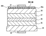
図3、4に基づいて、実施の形態2のLEDについて説明する。ここでは、図に示すようにp電極およびn電極が対向して配置されたLEDについて説明する。図3は、本実施の形態のLEDをp電極形成面側から見た概略図である。また、図4は、本実施の形態のLEDの層構成を示す模式的断面図であり、図3のA−A部における断面を表す。
【0026】
図4に示すように、本実施の形態の発光素子は、例えば、n型コンタクト層となるSiドープGaN層34、n型クラッド層となるSiドープGaN層35、活性層となるInGaN36、p型クラッド層となるMgドープAlGaN層37、p型コンタクト層となるMgドープGaN層38が、順次積層された層構造を有する。さらに、SiドープGaN層34にn電極39が形成され、MgドープGaN層38の略全面にp電極40が設けられている。なお、本実施の形態では、「特許請求の範囲」に記載するn型窒化物半導体がn型コンタクト層となるSiドープGaN層34に対応し、p型窒化物半導体がp型コンタクト層となるMgドープGaN層38に対応する。
【0027】
また、本実施の形態では、p電極形成面側から見て、p電極40上の略中央にワイヤーを接続するためのパッド部41が部分的に形成され、n電極39上及びパッド部41上の開口部を除き、各電極及び各半導体を覆うように絶縁膜(図示せず)が設けられている。なお、本実施の形態では、n電極39がワイヤーを接続するためのパッド部(図示せず)を含む構成とする。
【0028】
さらに、p電極40は、実施の形態1と同様に、第1の部材40aであるRhと、第2の部材40bであるAgより構成され、その構成は図3に示すように、第1の部材40aがメッシュ形状であり、かつ第2の部材40bがメッシュ形状の開口部内及び第1の部材40a上面に形成されている。メッシュ形状の第1の部材40aは、p型コンタクト層であるMgドープGaN層38の上面の略全域に渡って形成されている。必然的に、第1の部材40aの開口部に充填されている第2の部材40bも、p型コンタクト層であるMgドープGaN層38の上面の略全域に渡って形成されることになる。
【0029】
このように構成することで、実施の形態1と同様の効果を得ることができる。特に、本実施の形態のように各電極を対向するように配置する場合は、p電極側を実装基板に実装し、n電極側を視認側とすることが好ましい。これにより、n電極側を実装基板に実装しp電極側を視認側とする場合に比して、光の取り出し効率をより向上させることができる。
【0030】
また、本実施の形態のように、各電極を対向して配置させる場合は、接触抵抗が低い部材とp型窒化物半導体との接触面積を、p電極全体として不均一にすることができる。例えば、n電極直上に位置する部位近傍(図3ではp電極直下の部位近傍に相当する)におけるp型窒化物半導体との接触面積を他の部位に比較して小さくすることが好ましい。このように構成することにより、p電極とn電極を直線で結んだ部位近傍のみに電流を集中させずに、発光素子に流れる電流をより均一に全体に拡散させることができる。
【0031】
また、ここではp電極に部分的にパッド部を設ける構成としたが、p電極におけるパット部は必ずしも必要ない。すなわち、例えば、サファイア基板上に種々の半導体を成長させた後そのサファイア基板を除去する際、p電極に導電性接続部材である半田等を用いて金属基板を張り合わせた後にサファイア基板が除去される。これは、金属基板をp電極側に張り付けることによりある程度の厚みを確保し、サファイア基板を除去し易いようにするためである。このために、張り合わせられた金属基板を有する発光素子は、その金属基板自体がパッド部に相当することになる。なお、金属基板を構成する部材は特に限定されるものではないが、例えばCuとWの合金、AlとCuの合金等を用いることができる。
(実施の形態3)
特に図示はしないが、第1の部材と第2の部材の位置関係を逆転させる以外は、実施の形態1と同様に作製する。なお、本実施の形態においては、第2の部材であるAgを第1の部材であるRhで完全に覆う構成とすることがより好ましい。これにより、第2の部材であるAgのマイグレーションをさらに軽減させることができる。
(実施の形態4)
特に図示はしないが、第1の部材と第2の部材の位置関係を逆転させる以外は、実施の形態2と同様に作製する。このようにしても実施の形態2と同様に、光の取り出し効率を効果的に向上させることができる。なお、本実施の形態においては、第2の部材であるAgを第1の部材であるRhで完全に覆う構成とすることがより好ましい。これにより、第2の部材であるAgのマイグレーションをさらに軽減させることができる。
【0032】
実施の形態1〜4においては、第1の部材又は第2の部材の形状をメッシュ形状として説明したが、本発明は開口部を有していればよくメッシュ形状に限定されないことは言うまでもない。それ以外の形状としては、例えば、一方の部材を単にドット状に配置し、他の部材を少なくともドット間に充填することもできる。さらに、p電極は少なくとも第1の部材と第2の部材を備えていればよい。すなわち、本件発明の作用効果を阻害しないのであれば、さらに第3の部材、第4の部材等をp電極の構成に備えることもできる。
【0033】
【発明の効果】
以上説明した通り、本発明に係わる発光素子によれば、p電極における光の吸収を最小限に抑えることができる。これにより、光の取り出し効率を大幅に向上させることができる。また、マイグレーションを起こしやすいAg等の部材をp電極として用いても、そのマイグレーションを効果的に軽減することができる。
【図面の簡単な説明】
【図1】実施の形態1のLEDをp電極形成面側から見た平面図である。
【図2】図1のA−A部における断面図である。
【図3】実施の形態2のLEDをp電極形成面側から見た平面図である。
【図4】図3のA−A部における断面図である。
【符号の説明】
11・・・サファイア基板
12・・・GaNバッファ層
13・・・ノンドープGaN層
14、34・・・SiドープGaN層
15、35・・・SiドープGaN層
16、36・・・InGaN層
17、37・・・MgドープAlGaN層
18、38・・・MgドープGaN層
19、39・・・n電極
20、40・・・p電極
20a、40a・・・第1の部材
20b、40b・・・第2の部材
21、41・・・パッド[0001]
BACKGROUND OF THE INVENTION
The present invention relates to a light-emitting element including a nitride semiconductor (In X Al Y Ga 1-XY N, 0 ≦ X, 0 ≦ Y, X + Y ≦ 1) in a layer structure, and particularly, the light emission efficiency is dramatically improved. The present invention relates to a nitride semiconductor light emitting device.
[0002]
[Prior art]
Nitride semiconductor light-emitting elements including a nitride semiconductor in a layer structure are widely used in various fields such as high-luminance pure green light-emitting LEDs and blue light-emitting LEDs, such as full-color LED displays, traffic signal lights, and backlights.
[0003]
These LEDs generally have a structure in which various n-type nitride semiconductors or p-type nitride semiconductors according to purposes are stacked on a substrate such as sapphire. Furthermore, a p-electrode is disposed on the p-type nitride semiconductor, and an n-electrode is disposed on the n-type nitride semiconductor.
[0004]
[Problems to be solved by the invention]
However, with the current demand for LEDs capable of reducing power consumption without reducing light emission output due to energy saving or the like, the above configuration is not sufficient, and further improvement is required.
[0005]
That is, in the conventional LED described above, light emitted from the light emitting region is emitted from the upper surface and side surfaces of the LED via various semiconductors or substrates. More specifically, part of the light emitted from the light emitting region is reflected at every interface, that is, the interface between the substrate and the semiconductor, the interface between the semiconductor and the semiconductor, or the interface between the semiconductor and the electrode. And even if such a process is repeated a plurality of times, the light remaining without being absorbed by each member is emitted from the LED.
[0006]
Here, in order to make an electric current flow uniformly, the LED is mainly configured to have a p-electrode on substantially the entire surface of the p-type nitride semiconductor, but part of light is absorbed by the p-electrode itself provided on the entire surface. There was a problem that. As a result, part of the light from the light emitting region is wasted, and light cannot be efficiently extracted outside the LED. In addition to this, there is a problem that it is difficult to extend the life of the LED.
[0007]
In general, Ag is a highly reflective material and can be easily taken out by using it mainly for the p-electrode. However, it is difficult to stably reduce the contact resistance, and the power consumption should be sufficiently reduced. I can not. In addition, Ag is easily converted to positive ions and causes ion migration, and it is difficult to ensure sufficient reliability.
[0008]
The present invention has been made to solve such problems, and in particular, by providing a p-electrode with a specific configuration, the light extraction efficiency of the light-emitting element is further improved, and a light-emitting element with a long lifetime is provided. The purpose is to do.
[0009]
[Means for Solving the Problems]
The light emitting device of the present invention is a light emitting device having at least an n-type nitride semiconductor and a p-type nitride semiconductor, and having a p-electrode on a predetermined part of the p-type nitride semiconductor. In particular, the p-electrode has a first member having a contact resistance lower than that of the second member with respect to the p-type nitride semiconductor, and a second member having a reflectance higher than that of the first member with respect to light of the light emitting element. It is comprised at least from the member of,
The first member has an opening in which the p-type nitride semiconductor is exposed, before Symbol second member is Ag, is filled only in the opening, the first member upper surface It is not arranged . Thereby, the light from the light emitting element can be reflected by the first member or the second member, and the light can be efficiently extracted from the side surface or the vertical direction of the light emitting element. Further, by making the second member Ag, efficient light reflection can be obtained, and as a result, the light emission efficiency of the light emitting element can be improved. Further, since the p-electrode has the first member having a contact resistance lower than that of Ag, when the light emitting element is actually driven, current is mainly concentrated on the first member. Thereby, the movement of Ag, that is, ion migration can be suppressed and the reliability can be improved.
[0010]
Further, the first member is a mesh shape having a plurality of openings, it said and said second member into the opening of the mesh shape is filled, the second member to said first member Preferably they are surrounded . Thereby, since the 2nd member is filled into a plurality of openings, the 2nd member can be arranged more evenly.
[0011]
The first member preferably includes at least one element selected from Ni, Au, Rh, Ir, and Pd. Thereby, ohmic contact can be obtained easily.
[0012]
Further, in a light emitting device having at least an n-type nitride semiconductor and a p-type nitride semiconductor and including a p-electrode on a predetermined part of the p-type nitride semiconductor, the p-electrode includes Ni, Au, Rh, Ir , At least one element including at least one element selected from Pd , and a second member that is Ag having higher reflectivity than the first member with respect to the light of the light emitting element. , the first member is a mesh shape having a plurality of openings in which the p-type nitride semiconductor is exposed, before Symbol the second member, the opening of the mesh shape as surrounded by the first member It is characterized by being filled in the part.
Furthermore, an n-electrode provided on the n-type nitride semiconductor is provided on the same surface side as the p-electrode, and a contact area between the first member and the p-type nitride semiconductor is determined by the formation of the p-electrode. When viewed from the surface side, it can be gradually increased as the distance from the n-electrode increases.
Alternatively, the n-type electrode provided on the n-type nitride semiconductor is provided on the side facing the p-electrode, and the first member and the p-type nitride semiconductor in the vicinity of a portion located immediately above the n-electrode The contact area can be made smaller than the contact area between the first member and the p-type nitride semiconductor at other sites.
[0013]
DETAILED DESCRIPTION OF THE INVENTION
In this embodiment, an example in which an LED (Light Emitting Diode) is used as a light emitting element will be described. As each semiconductor layer constituting the LED according to the present invention, various nitride semiconductors can be used. For example, metal organic chemical vapor deposition (MOCVD), hydride vapor phase epitaxy (HVPE) In X Al Y Ga 1-XY N ( where, 0 ≦ X, 0 ≦ Y , X + Y ≦ 1) such as by a made of a semiconductor It can be used suitably. As the layer structure, a known layer structure can be used. For example, a homostructure, a single heterostructure, or a double heterostructure having a MIS junction, a PIN junction, or a PN junction can be used. In addition, a specific layer may have a superlattice structure, or a single quantum well structure or a multiple quantum well structure in which an active layer is formed in a thin film that produces a quantum effect. Furthermore, various known phosphors can be disposed at predetermined positions of the light emitting element, and light from the light emitting element can be converted into desired light.
[0014]
Further, the LED is generally formed by growing each semiconductor layer on a specific substrate. At that time, when an insulating substrate is used as the substrate and the insulating substrate is not finally removed, usually, Both the p electrode and the n electrode are formed on the same surface side of the LED. In this case, it is possible to take out the emitted light from the semiconductor side with the face-up mounting, i.e. the semiconductor side placed on the viewing side, or with the face-down mounting, i.e. the board side placed on the viewing side, It is also possible to take it out from. Of course, it is also possible to adopt a configuration in which the p-electrode and the n-electrode are arranged to face each other with the semiconductor layer structure by not using the insulating substrate from the beginning or finally removing the insulating substrate.
[0015]
Hereinafter, embodiments of the present invention will be described with reference to the drawings. However, the embodiment described below exemplifies an LED for embodying the technical idea of the present invention, and does not specify the LED of the present invention as follows. Further, the size and positional relationship of the members shown in each drawing may be exaggerated for clarity of explanation.
(Embodiment 1)
The LED according to the first embodiment will be described with reference to FIGS. Here, as shown in the figure, an LED in which a p-electrode and an n-electrode are arranged on the same surface side will be described. FIG. 1 is a schematic view of the LED of the present embodiment as viewed from the electrode forming surface side. FIG. 2 is a schematic cross-sectional view showing the layer structure of the LED of the present embodiment, and represents a cross section taken along the line AA of FIG.
[0016]
As shown in FIG. 2, the light emitting device of this embodiment includes, for example, a
[0017]
In the present embodiment, a
[0018]
Here, the p-
[0019]
In this way, when the
[0020]
However, as in the present invention, by making Rh, which is the
[0021]
Furthermore, since Ag is a member having a very high reflectance in most of the wavelengths that can be emitted by the nitride semiconductor, the opening of the
[0022]
Furthermore, when a member having high reflectance such as Ag is used as the second member and ohmic annealing (heat treatment for ohmic contact) is performed on the first member having low contact resistance, as in the present embodiment, It is preferable to form the second member in the opening of the first member and on the upper surface. That is, generally, a member having a high reflectance such as Ag tends to have a reduced reflectance when heat-treated. However, after the first member having a low contact resistance is first formed on the p-type semiconductor and subjected to ohmic annealing, the second member is further disposed in the opening and on the upper surface of the first member, whereby the second member The p-electrode can be formed without affecting the heat.
[0023]
Further, as in the present embodiment, the
[0024]
In the present embodiment, the mesh-shaped openings are arranged uniformly over the entire p-electrode, but the present invention is not limited to this. For example, the contact area between the low contact resistance member and the p-type contact layer is configured to gradually increase as the distance from the n-electrode is viewed from the electrode forming surface side so that current flows uniformly through the entire LED. May be. That is, the shape, size, arrangement position, and the like of the opening can be arbitrarily set on the designer side.
[0025]
On the other hand, the
(Embodiment 2)
The LED according to the second embodiment will be described with reference to FIGS. Here, an LED in which a p-electrode and an n-electrode are arranged to face each other as shown in the drawing will be described. FIG. 3 is a schematic view of the LED of the present embodiment as viewed from the p-electrode formation surface side. FIG. 4 is a schematic cross-sectional view showing the layer structure of the LED of the present embodiment, and shows a cross section taken along the line AA of FIG.
[0026]
As shown in FIG. 4, the light emitting device of the present embodiment includes, for example, a Si-doped
[0027]
In the present embodiment, as viewed from the p-electrode forming surface side, a
[0028]
Further, the p-
[0029]
By configuring in this way, the same effect as in the first embodiment can be obtained. In particular, when the electrodes are arranged to face each other as in the present embodiment, it is preferable that the p electrode side is mounted on the mounting substrate and the n electrode side is the viewing side. Thereby, compared with the case where the n electrode side is mounted on the mounting substrate and the p electrode side is the viewing side, the light extraction efficiency can be further improved.
[0030]
Further, when the electrodes are arranged to face each other as in the present embodiment, the contact area between the member having low contact resistance and the p-type nitride semiconductor can be made non-uniform for the entire p electrode. For example, it is preferable to reduce the contact area with the p-type nitride semiconductor in the vicinity of the portion located immediately above the n electrode (corresponding to the vicinity of the portion immediately below the p electrode in FIG. 3) compared to other portions. By configuring in this way, the current flowing through the light emitting element can be more uniformly diffused without concentrating the current only in the vicinity of the portion where the p electrode and the n electrode are connected by a straight line.
[0031]
Here, the pad portion is partially provided on the p electrode, but the pad portion on the p electrode is not necessarily required. That is, for example, when various semiconductors are grown on a sapphire substrate and then the sapphire substrate is removed, the sapphire substrate is removed after bonding the metal substrate to the p-electrode using solder or the like as a conductive connecting member. . This is to secure a certain thickness by sticking the metal substrate to the p-electrode side and to facilitate removal of the sapphire substrate. For this reason, in the light emitting element having the bonded metal substrate, the metal substrate itself corresponds to the pad portion. In addition, although the member which comprises a metal substrate is not specifically limited, For example, the alloy of Cu and W, the alloy of Al and Cu, etc. can be used.
(Embodiment 3)
Although not shown in the drawing, it is manufactured in the same manner as in Embodiment 1 except that the positional relationship between the first member and the second member is reversed. In the present embodiment, it is more preferable that Ag as the second member is completely covered with Rh as the first member. Thereby, the migration of Ag as the second member can be further reduced.
(Embodiment 4)
Although not shown in the drawing, it is manufactured in the same manner as in Embodiment 2 except that the positional relationship between the first member and the second member is reversed. Even in this case, similarly to the second embodiment, the light extraction efficiency can be effectively improved. In the present embodiment, it is more preferable that Ag as the second member is completely covered with Rh as the first member. Thereby, the migration of Ag as the second member can be further reduced.
[0032]
In Embodiment 1-4, although the shape of the 1st member or the 2nd member was demonstrated as a mesh shape, it cannot be overemphasized that this invention should just have an opening part and is not limited to a mesh shape. As other shapes, for example, one member can be simply arranged in a dot shape, and the other member can be filled at least between the dots. Further, the p-electrode only needs to include at least a first member and a second member. That is, as long as the effects of the present invention are not hindered, the third member, the fourth member, and the like can be further provided in the configuration of the p-electrode.
[0033]
【The invention's effect】
As described above, according to the light emitting device of the present invention, light absorption at the p-electrode can be minimized. Thereby, the light extraction efficiency can be significantly improved. Further, even when a member such as Ag that easily causes migration is used as the p-electrode, the migration can be effectively reduced.
[Brief description of the drawings]
FIG. 1 is a plan view of an LED according to a first embodiment when viewed from a p-electrode formation surface side.
FIG. 2 is a cross-sectional view taken along a line AA in FIG.
FIG. 3 is a plan view of the LED according to the second embodiment as viewed from the p-electrode formation surface side.
4 is a cross-sectional view taken along a line AA in FIG.
[Explanation of symbols]
11 ...
Claims (6)
前記p電極は、前記p型窒化物半導体に対して第2の部材よりも接触抵抗が低い第1の部材と、前記発光素子の光に対して第1の部材よりも反射率の高い第2の部材から少なくとも構成され、
前記第1の部材は、前記p型窒化物半導体が露出した開口部を有し、
前記第2の部材はAgであり、前記開口部内のみに充填されており、前記第1の部材上面に配置されていないことを特徴とする発光素子。In a light emitting device having at least an n-type nitride semiconductor and a p-type nitride semiconductor, and having a p-electrode on a predetermined part of the p-type nitride semiconductor,
The p-electrode includes a first member having a lower contact resistance than the second member with respect to the p-type nitride semiconductor, and a second member having a higher reflectance than the first member with respect to the light of the light emitting element. Consisting of at least members of
The first member has an opening from which the p-type nitride semiconductor is exposed,
Before Stories second member is Ag, is filled only in the opening, the light emitting device characterized by not disposed in the first member upper surface.
前記p電極は、Ni、Au、Rh、Ir、Pdから選択された少なくとも1つの元素を含む構成である第1の部材と、前記発光素子の光に対して第1の部材よりも反射率の高いAgである第2の部材から少なくとも構成され、
前記第1の部材は、前記p型窒化物半導体が露出した開口部を複数有するメッシュ形状であり、
前記第2の部材は、前記第1の部材に取り囲まれるように前記メッシュ形状の開口部内に充填されていることを特徴とする発光素子。In a light emitting device having at least an n-type nitride semiconductor and a p-type nitride semiconductor, and having a p-electrode on a predetermined part of the p-type nitride semiconductor,
The p-electrode has a first member configured to include at least one element selected from Ni, Au, Rh, Ir, and Pd, and has a reflectance higher than that of the first member with respect to the light of the light-emitting element. Composed of at least a second member that is high Ag,
The first member has a mesh shape having a plurality of openings from which the p-type nitride semiconductor is exposed ,
Before SL and the second member, the light emitting element characterized in that it is filled in the opening of the mesh shape as surrounded by the first member.
前記第1の部材と前記p型窒化物半導体との接触面積は、前記p電極の形成面側から見て、前記n電極から離れるに従って徐々に大きくなっていることを特徴とする請求項1〜4のいずれか一に記載の発光素子。 An n electrode provided on the n-type nitride semiconductor is provided on the same side as the p electrode,
2. The contact area between the first member and the p-type nitride semiconductor is gradually increased as the distance from the n electrode is increased as viewed from the p electrode forming surface side . 5. The light emitting device according to any one of 4.
前記n電極直上に位置する部位近傍における前記第1の部材と前記p型窒化物半導体との接触面積は、他の部位における前記第1の部材と前記p型窒化物半導体との接触面積よりも小さいことを特徴とする請求項1〜4のいずれか一に記載の発光素子。 An n electrode provided on the n-type nitride semiconductor is provided on the surface facing the p electrode,
The contact area between the first member and the p-type nitride semiconductor in the vicinity of the part located immediately above the n electrode is larger than the contact area between the first member and the p-type nitride semiconductor in the other part. the light emitting device according to any one of claims 1 to 4, characterized in that small.
Priority Applications (1)
| Application Number | Priority Date | Filing Date | Title |
|---|---|---|---|
| JP2002225268A JP4239508B2 (en) | 2002-08-01 | 2002-08-01 | Light emitting element |
Applications Claiming Priority (1)
| Application Number | Priority Date | Filing Date | Title |
|---|---|---|---|
| JP2002225268A JP4239508B2 (en) | 2002-08-01 | 2002-08-01 | Light emitting element |
Publications (3)
| Publication Number | Publication Date |
|---|---|
| JP2004071655A JP2004071655A (en) | 2004-03-04 |
| JP2004071655A5 JP2004071655A5 (en) | 2005-10-27 |
| JP4239508B2 true JP4239508B2 (en) | 2009-03-18 |
Family
ID=32012990
Family Applications (1)
| Application Number | Title | Priority Date | Filing Date |
|---|---|---|---|
| JP2002225268A Expired - Fee Related JP4239508B2 (en) | 2002-08-01 | 2002-08-01 | Light emitting element |
Country Status (1)
| Country | Link |
|---|---|
| JP (1) | JP4239508B2 (en) |
Families Citing this family (25)
| Publication number | Priority date | Publication date | Assignee | Title |
|---|---|---|---|---|
| KR100799857B1 (en) * | 2003-10-27 | 2008-01-31 | 삼성전기주식회사 | Electrode structure and semiconductor light-emitting device provided with the same |
| KR100586949B1 (en) * | 2004-01-19 | 2006-06-07 | 삼성전기주식회사 | Flip chip type nitride semiconductor light emitting diode |
| JP2006066868A (en) | 2004-03-23 | 2006-03-09 | Toyoda Gosei Co Ltd | Solid-state component and solid-state component device |
| KR100631840B1 (en) * | 2004-06-03 | 2006-10-09 | 삼성전기주식회사 | Nitride semiconductor light emitting device for flip chip |
| KR100576870B1 (en) | 2004-08-11 | 2006-05-10 | 삼성전기주식회사 | Nitride semiconductor light emitting diode and method of producing the same |
| US7291865B2 (en) | 2004-09-29 | 2007-11-06 | Toyoda Gosei Co., Ltd. | Light-emitting semiconductor device |
| JP4622426B2 (en) * | 2004-09-29 | 2011-02-02 | 豊田合成株式会社 | Semiconductor light emitting device |
| US7436066B2 (en) | 2004-10-19 | 2008-10-14 | Nichia Corporation | Semiconductor element |
| KR100601992B1 (en) * | 2005-02-16 | 2006-07-18 | 삼성전기주식회사 | Reflective electrode and compound semiconductor light emitting device including the same |
| JP4967243B2 (en) * | 2005-03-08 | 2012-07-04 | 三菱化学株式会社 | GaN-based light emitting diode and light emitting device |
| CN100369279C (en) * | 2005-05-27 | 2008-02-13 | 中国科学院物理研究所 | Bridge N-electrode type gallium nitride base large tube core LED and preparation method |
| JP2007027540A (en) * | 2005-07-20 | 2007-02-01 | Matsushita Electric Ind Co Ltd | Semiconductor light-emitting device and illuminator using same |
| JP2007027539A (en) * | 2005-07-20 | 2007-02-01 | Matsushita Electric Ind Co Ltd | Semiconductor light-emitting device and illuminator using same |
| US7439548B2 (en) * | 2006-08-11 | 2008-10-21 | Bridgelux, Inc | Surface mountable chip |
| US7714340B2 (en) * | 2006-09-06 | 2010-05-11 | Palo Alto Research Center Incorporated | Nitride light-emitting device |
| JP5176334B2 (en) * | 2007-02-01 | 2013-04-03 | 日亜化学工業株式会社 | Semiconductor light emitting device |
| JP2009238931A (en) * | 2008-03-26 | 2009-10-15 | Panasonic Electric Works Co Ltd | Semiconductor light-emitting element and manufacturing method therefor, and luminaire using the element |
| JP5361569B2 (en) * | 2008-06-26 | 2013-12-04 | 京セラ株式会社 | Semiconductor light emitting device and manufacturing method thereof |
| JP5197186B2 (en) | 2008-06-30 | 2013-05-15 | 株式会社東芝 | Semiconductor light emitting device |
| US8536595B2 (en) | 2010-08-31 | 2013-09-17 | Micron Technology, Inc. | Solid state lighting devices with low contact resistance and methods of manufacturing |
| JP2012186195A (en) | 2011-03-03 | 2012-09-27 | Toshiba Corp | Semiconductor light-emitting element and method of manufacturing the same |
| JP5321656B2 (en) * | 2011-08-05 | 2013-10-23 | 三菱化学株式会社 | GaN-based light emitting diode and light emitting device |
| DE102012107384A1 (en) | 2012-08-10 | 2014-02-13 | Osram Opto Semiconductors Gmbh | Optoelectronic semiconductor component and method for producing a mirror region on a semiconductor body |
| JP2013062535A (en) * | 2012-12-18 | 2013-04-04 | Toshiba Corp | Semiconductor light-emitting device and method of manufacturing the same |
| DE102019103638A1 (en) * | 2019-02-13 | 2020-08-13 | OSRAM Opto Semiconductors Gesellschaft mit beschränkter Haftung | OPTOELECTRONIC SEMICONDUCTOR COMPONENT WITH SECTIONS OF A CONDUCTIVE LAYER AND A METHOD FOR MANUFACTURING AN OPTOELECTRONIC SEMICONDUCTOR COMPONENT |
-
2002
- 2002-08-01 JP JP2002225268A patent/JP4239508B2/en not_active Expired - Fee Related
Also Published As
| Publication number | Publication date |
|---|---|
| JP2004071655A (en) | 2004-03-04 |
Similar Documents
| Publication | Publication Date | Title |
|---|---|---|
| JP4239508B2 (en) | Light emitting element | |
| KR100838197B1 (en) | Light emitting diode with improved current spreading performance | |
| KR101064053B1 (en) | Light emitting device and manufacturing method | |
| KR101064006B1 (en) | Light emitting element | |
| JP4564726B2 (en) | Contact system for large area and small area semiconductor light emitting flip chip devices | |
| US8581295B2 (en) | Semiconductor light-emitting diode | |
| EP2221873B1 (en) | Light emitting device | |
| KR100999726B1 (en) | Light emitting device and method for fabricating the same | |
| KR101276053B1 (en) | Semiconductor light emitting device and light emitting apparatus | |
| JP5816243B2 (en) | Light emitting device and light emitting device package | |
| US9450017B2 (en) | Semiconductor light emitting device and method of fabricating the same | |
| US20110095332A1 (en) | Light emitting device, light emitting device package, and lighting system | |
| US11430934B2 (en) | Light-emitting diode device | |
| US20230253528A1 (en) | Solid state lighting devices with improved current spreading and light extraction and associated methods | |
| KR101114047B1 (en) | Light emitting device and method for fabricating the same | |
| JP2013254939A (en) | Light emitting element and light emitting element package | |
| KR100992728B1 (en) | Light emitting device and method for fabricating the same | |
| US20100230703A1 (en) | Light emitting device fabrication method thereof, and light emitting apparatus | |
| KR102234117B1 (en) | Light emitting device and lighting system | |
| KR101231477B1 (en) | Light emitting device | |
| KR101710889B1 (en) | Light Emitting Device | |
| KR100661715B1 (en) | light emitting diode having island-type interlayer and manufacturing method thereof | |
| KR101633814B1 (en) | light emitting device | |
| KR20120065704A (en) | Light emitting diode and method for fabricating the light emitting device | |
| KR20170017630A (en) | Light emitting device and light emitting device package |
Legal Events
| Date | Code | Title | Description |
|---|---|---|---|
| A521 | Request for written amendment filed |
Free format text: JAPANESE INTERMEDIATE CODE: A523 Effective date: 20050729 |
|
| A621 | Written request for application examination |
Free format text: JAPANESE INTERMEDIATE CODE: A621 Effective date: 20050729 |
|
| A977 | Report on retrieval |
Free format text: JAPANESE INTERMEDIATE CODE: A971007 Effective date: 20080623 |
|
| A131 | Notification of reasons for refusal |
Free format text: JAPANESE INTERMEDIATE CODE: A131 Effective date: 20080701 |
|
| A521 | Request for written amendment filed |
Free format text: JAPANESE INTERMEDIATE CODE: A821 Effective date: 20080811 |
|
| RD02 | Notification of acceptance of power of attorney |
Free format text: JAPANESE INTERMEDIATE CODE: A7422 Effective date: 20080811 |
|
| A521 | Request for written amendment filed |
Free format text: JAPANESE INTERMEDIATE CODE: A523 Effective date: 20080901 |
|
| TRDD | Decision of grant or rejection written | ||
| A01 | Written decision to grant a patent or to grant a registration (utility model) |
Free format text: JAPANESE INTERMEDIATE CODE: A01 Effective date: 20081202 |
|
| A01 | Written decision to grant a patent or to grant a registration (utility model) |
Free format text: JAPANESE INTERMEDIATE CODE: A01 |
|
| A61 | First payment of annual fees (during grant procedure) |
Free format text: JAPANESE INTERMEDIATE CODE: A61 Effective date: 20081215 |
|
| FPAY | Renewal fee payment (event date is renewal date of database) |
Free format text: PAYMENT UNTIL: 20120109 Year of fee payment: 3 |
|
| R150 | Certificate of patent or registration of utility model |
Ref document number: 4239508 Country of ref document: JP Free format text: JAPANESE INTERMEDIATE CODE: R150 Free format text: JAPANESE INTERMEDIATE CODE: R150 |
|
| FPAY | Renewal fee payment (event date is renewal date of database) |
Free format text: PAYMENT UNTIL: 20120109 Year of fee payment: 3 |
|
| FPAY | Renewal fee payment (event date is renewal date of database) |
Free format text: PAYMENT UNTIL: 20120109 Year of fee payment: 3 |
|
| FPAY | Renewal fee payment (event date is renewal date of database) |
Free format text: PAYMENT UNTIL: 20120109 Year of fee payment: 3 |
|
| FPAY | Renewal fee payment (event date is renewal date of database) |
Free format text: PAYMENT UNTIL: 20130109 Year of fee payment: 4 |
|
| R250 | Receipt of annual fees |
Free format text: JAPANESE INTERMEDIATE CODE: R250 |
|
| FPAY | Renewal fee payment (event date is renewal date of database) |
Free format text: PAYMENT UNTIL: 20130109 Year of fee payment: 4 |
|
| FPAY | Renewal fee payment (event date is renewal date of database) |
Free format text: PAYMENT UNTIL: 20140109 Year of fee payment: 5 |
|
| R250 | Receipt of annual fees |
Free format text: JAPANESE INTERMEDIATE CODE: R250 |
|
| R250 | Receipt of annual fees |
Free format text: JAPANESE INTERMEDIATE CODE: R250 |
|
| R250 | Receipt of annual fees |
Free format text: JAPANESE INTERMEDIATE CODE: R250 |
|
| R250 | Receipt of annual fees |
Free format text: JAPANESE INTERMEDIATE CODE: R250 |
|
| R250 | Receipt of annual fees |
Free format text: JAPANESE INTERMEDIATE CODE: R250 |
|
| R250 | Receipt of annual fees |
Free format text: JAPANESE INTERMEDIATE CODE: R250 |
|
| R250 | Receipt of annual fees |
Free format text: JAPANESE INTERMEDIATE CODE: R250 |
|
| R250 | Receipt of annual fees |
Free format text: JAPANESE INTERMEDIATE CODE: R250 |
|
| R250 | Receipt of annual fees |
Free format text: JAPANESE INTERMEDIATE CODE: R250 |
|
| LAPS | Cancellation because of no payment of annual fees |