JP4225183B2 - Manufacturing method of semiconductor device - Google Patents
Manufacturing method of semiconductor device Download PDFInfo
- Publication number
- JP4225183B2 JP4225183B2 JP2003375319A JP2003375319A JP4225183B2 JP 4225183 B2 JP4225183 B2 JP 4225183B2 JP 2003375319 A JP2003375319 A JP 2003375319A JP 2003375319 A JP2003375319 A JP 2003375319A JP 4225183 B2 JP4225183 B2 JP 4225183B2
- Authority
- JP
- Japan
- Prior art keywords
- solvent
- containing resin
- resin
- manufacturing
- heating
- Prior art date
- Legal status (The legal status is an assumption and is not a legal conclusion. Google has not performed a legal analysis and makes no representation as to the accuracy of the status listed.)
- Expired - Fee Related
Links
Images


Classifications
-
- H—ELECTRICITY
- H01—ELECTRIC ELEMENTS
- H01L—SEMICONDUCTOR DEVICES NOT COVERED BY CLASS H10
- H01L2224/00—Indexing scheme for arrangements for connecting or disconnecting semiconductor or solid-state bodies and methods related thereto as covered by H01L24/00
- H01L2224/01—Means for bonding being attached to, or being formed on, the surface to be connected, e.g. chip-to-package, die-attach, "first-level" interconnects; Manufacturing methods related thereto
- H01L2224/26—Layer connectors, e.g. plate connectors, solder or adhesive layers; Manufacturing methods related thereto
- H01L2224/2612—Auxiliary members for layer connectors, e.g. spacers
-
- H—ELECTRICITY
- H01—ELECTRIC ELEMENTS
- H01L—SEMICONDUCTOR DEVICES NOT COVERED BY CLASS H10
- H01L2224/00—Indexing scheme for arrangements for connecting or disconnecting semiconductor or solid-state bodies and methods related thereto as covered by H01L24/00
- H01L2224/01—Means for bonding being attached to, or being formed on, the surface to be connected, e.g. chip-to-package, die-attach, "first-level" interconnects; Manufacturing methods related thereto
- H01L2224/26—Layer connectors, e.g. plate connectors, solder or adhesive layers; Manufacturing methods related thereto
- H01L2224/31—Structure, shape, material or disposition of the layer connectors after the connecting process
- H01L2224/32—Structure, shape, material or disposition of the layer connectors after the connecting process of an individual layer connector
- H01L2224/321—Disposition
- H01L2224/32151—Disposition the layer connector connecting between a semiconductor or solid-state body and an item not being a semiconductor or solid-state body, e.g. chip-to-substrate, chip-to-passive
- H01L2224/32221—Disposition the layer connector connecting between a semiconductor or solid-state body and an item not being a semiconductor or solid-state body, e.g. chip-to-substrate, chip-to-passive the body and the item being stacked
- H01L2224/32245—Disposition the layer connector connecting between a semiconductor or solid-state body and an item not being a semiconductor or solid-state body, e.g. chip-to-substrate, chip-to-passive the body and the item being stacked the item being metallic
-
- H—ELECTRICITY
- H01—ELECTRIC ELEMENTS
- H01L—SEMICONDUCTOR DEVICES NOT COVERED BY CLASS H10
- H01L2224/00—Indexing scheme for arrangements for connecting or disconnecting semiconductor or solid-state bodies and methods related thereto as covered by H01L24/00
- H01L2224/01—Means for bonding being attached to, or being formed on, the surface to be connected, e.g. chip-to-package, die-attach, "first-level" interconnects; Manufacturing methods related thereto
- H01L2224/42—Wire connectors; Manufacturing methods related thereto
- H01L2224/47—Structure, shape, material or disposition of the wire connectors after the connecting process
- H01L2224/48—Structure, shape, material or disposition of the wire connectors after the connecting process of an individual wire connector
- H01L2224/481—Disposition
- H01L2224/48151—Connecting between a semiconductor or solid-state body and an item not being a semiconductor or solid-state body, e.g. chip-to-substrate, chip-to-passive
- H01L2224/48221—Connecting between a semiconductor or solid-state body and an item not being a semiconductor or solid-state body, e.g. chip-to-substrate, chip-to-passive the body and the item being stacked
- H01L2224/48245—Connecting between a semiconductor or solid-state body and an item not being a semiconductor or solid-state body, e.g. chip-to-substrate, chip-to-passive the body and the item being stacked the item being metallic
- H01L2224/48247—Connecting between a semiconductor or solid-state body and an item not being a semiconductor or solid-state body, e.g. chip-to-substrate, chip-to-passive the body and the item being stacked the item being metallic connecting the wire to a bond pad of the item
-
- H—ELECTRICITY
- H01—ELECTRIC ELEMENTS
- H01L—SEMICONDUCTOR DEVICES NOT COVERED BY CLASS H10
- H01L2224/00—Indexing scheme for arrangements for connecting or disconnecting semiconductor or solid-state bodies and methods related thereto as covered by H01L24/00
- H01L2224/73—Means for bonding being of different types provided for in two or more of groups H01L2224/10, H01L2224/18, H01L2224/26, H01L2224/34, H01L2224/42, H01L2224/50, H01L2224/63, H01L2224/71
- H01L2224/732—Location after the connecting process
- H01L2224/73251—Location after the connecting process on different surfaces
- H01L2224/73265—Layer and wire connectors
-
- H—ELECTRICITY
- H01—ELECTRIC ELEMENTS
- H01L—SEMICONDUCTOR DEVICES NOT COVERED BY CLASS H10
- H01L2224/00—Indexing scheme for arrangements for connecting or disconnecting semiconductor or solid-state bodies and methods related thereto as covered by H01L24/00
- H01L2224/80—Methods for connecting semiconductor or other solid state bodies using means for bonding being attached to, or being formed on, the surface to be connected
- H01L2224/83—Methods for connecting semiconductor or other solid state bodies using means for bonding being attached to, or being formed on, the surface to be connected using a layer connector
- H01L2224/83909—Post-treatment of the layer connector or bonding area
- H01L2224/83951—Forming additional members, e.g. for reinforcing, fillet sealant
-
- H—ELECTRICITY
- H01—ELECTRIC ELEMENTS
- H01L—SEMICONDUCTOR DEVICES NOT COVERED BY CLASS H10
- H01L2224/00—Indexing scheme for arrangements for connecting or disconnecting semiconductor or solid-state bodies and methods related thereto as covered by H01L24/00
- H01L2224/80—Methods for connecting semiconductor or other solid state bodies using means for bonding being attached to, or being formed on, the surface to be connected
- H01L2224/85—Methods for connecting semiconductor or other solid state bodies using means for bonding being attached to, or being formed on, the surface to be connected using a wire connector
- H01L2224/85909—Post-treatment of the connector or wire bonding area
- H01L2224/8592—Applying permanent coating, e.g. protective coating
-
- H—ELECTRICITY
- H01—ELECTRIC ELEMENTS
- H01L—SEMICONDUCTOR DEVICES NOT COVERED BY CLASS H10
- H01L2924/00—Indexing scheme for arrangements or methods for connecting or disconnecting semiconductor or solid-state bodies as covered by H01L24/00
- H01L2924/10—Details of semiconductor or other solid state devices to be connected
- H01L2924/11—Device type
- H01L2924/13—Discrete devices, e.g. 3 terminal devices
- H01L2924/1301—Thyristor
-
- H—ELECTRICITY
- H01—ELECTRIC ELEMENTS
- H01L—SEMICONDUCTOR DEVICES NOT COVERED BY CLASS H10
- H01L2924/00—Indexing scheme for arrangements or methods for connecting or disconnecting semiconductor or solid-state bodies as covered by H01L24/00
- H01L2924/10—Details of semiconductor or other solid state devices to be connected
- H01L2924/11—Device type
- H01L2924/13—Discrete devices, e.g. 3 terminal devices
- H01L2924/1304—Transistor
- H01L2924/1305—Bipolar Junction Transistor [BJT]
- H01L2924/13055—Insulated gate bipolar transistor [IGBT]
-
- H—ELECTRICITY
- H01—ELECTRIC ELEMENTS
- H01L—SEMICONDUCTOR DEVICES NOT COVERED BY CLASS H10
- H01L2924/00—Indexing scheme for arrangements or methods for connecting or disconnecting semiconductor or solid-state bodies as covered by H01L24/00
- H01L2924/15—Details of package parts other than the semiconductor or other solid state devices to be connected
- H01L2924/181—Encapsulation
Landscapes
- Structures Or Materials For Encapsulating Or Coating Semiconductor Devices Or Solid State Devices (AREA)
- Encapsulation Of And Coatings For Semiconductor Or Solid State Devices (AREA)
Description
本発明は、発熱素子の両面に放熱板を配設してなる装置を用意し、この装置のほぼ全体をモールド樹脂でモールドする半導体装置の製造方法に関し、特に、装置をモールドする前に、放熱板とモールド樹脂との接着力を向上させるための溶剤含有型樹脂を装置に塗布するようにした製造方法に関する。 The present invention relates to a method of manufacturing a semiconductor device in which a heat sink is provided on both sides of a heat generating element, and the entire device is molded with a mold resin. In particular, the heat dissipation is performed before the device is molded. The present invention relates to a manufacturing method in which a solvent-containing resin for improving the adhesive force between a plate and a mold resin is applied to an apparatus.
従来より、発熱素子とこの発熱素子の両面から放熱するための一対の放熱板とを備える装置を用意し、当該装置のほぼ全体をモールド樹脂でモールドするようにした半導体装置の製造方法が提案されている(たとえば、特許文献1参照)。 Conventionally, a method of manufacturing a semiconductor device has been proposed in which a device including a heat generating element and a pair of heat radiating plates for radiating heat from both sides of the heat generating element is prepared, and almost the entire device is molded with a mold resin. (For example, refer to Patent Document 1).
この製造方法では、上記装置を用意した後モールド樹脂でモールドする前に、この装置の表面に溶剤を含有してなる溶剤含有型樹脂を塗布することにより、金属体である放熱板とモールド樹脂との接着力を向上させるようにしている。 In this manufacturing method, after preparing the above device and before molding with a mold resin, by applying a solvent-containing resin containing a solvent to the surface of this device, a heat sink and a mold resin, which are metal bodies, To improve the adhesive strength.
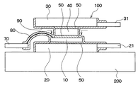
図4は、従来の一般的な、溶剤含有型樹脂の塗布方法を示す概略断面図である。 FIG. 4 is a schematic cross-sectional view showing a conventional general method for applying a solvent-containing resin.
図4に示される装置100では、発熱素子10の下面には接合材50を介して第1の放熱板としての下側ヒートシンク20が接合され、発熱素子10の上面には、接合材50、ヒートシンクブロック40、接合材50を介して第2の放熱板としての上側ヒートシンク30が接合されている。
In the
そして、この装置100に対して、溶剤含有型樹脂90を塗布する。溶剤含有型樹脂90としては、たとえば、ポリアミド等の樹脂にアルコール等の溶剤を含有させたものが採用される。
Then, a solvent-containing
この溶剤含有型樹脂90の塗布方法としては、たとえば装置100の溶剤含有型樹脂90へのディッピングにより行ったり、溶剤含有型樹脂90をディスペンサのノズルから滴下もしくは噴霧したりする方法を採用することができる。
As a method for applying the solvent-containing
そして、溶剤含有型樹脂90が塗布された装置100を加熱して、溶剤含有型樹脂90の乾燥を行う。
Then, the
具体的には、下側ヒートシンク20を下方にし、上側ヒートシンク30を上方にして、加熱部材としての熱板200の上に、この装置100を搭載することによって、溶剤含有型樹脂90の乾燥を行うものである。
しかしながら、従来では、上記図4に示されるように、下側ヒートシンク20を下方に位置させた状態にて、溶剤含有型樹脂90の乾燥を行っていたが、上側ヒートシンク30が下側ヒートシンク20の上に存在した状態で加熱が行われるため、以下のような問題が生じる。
However, conventionally, as shown in FIG. 4, the solvent-containing
一つは、従来の下側ヒートシンク20を熱板200で加熱する方法では、上側ヒートシンク30は金属体を伝わる熱と雰囲気熱とによって主に加熱される。しかし、この場合、下側ヒートシンク20と上側ヒートシンク30とで温度差が生じ、溶剤含有型樹脂90が一様に形成されない場合がある。
One is a conventional method in which the
もう一つは、従来の方法では、上側ヒートシンク30において溶剤含有型樹脂90が塗布された下面が重力方向を向いているため、液体状の溶剤含有型樹脂90が、図4中の矢印に示されるように、下方へ流れたり落下したりする。それにより、溶剤含有型樹脂90が一様に形成されない場合がある。
The other is that in the conventional method, since the lower surface of the upper heat sink 30 on which the solvent-containing
このように、溶剤含有型樹脂90が一様に形成されない場合、その後、装置100をモールド樹脂でモールドしたときに、モールド樹脂とヒートシンクとの接着力が確保できず、モールド樹脂の剥離が生じる可能性がある。そして、このような剥離は、モールド樹脂のクラック、果てには、ワイヤボンディングのクラック等につながり、装置100の機能不良に至ることとなる。
As described above, when the solvent-containing
そこで、本発明は上記問題に鑑み、発熱素子の両面に一対の放熱板を配設してなる装置に対して、溶剤含有型樹脂を塗布した後、当該装置のほぼ全体をモールド樹脂でモールドするようにした半導体装置の製造方法において、装置に対して溶剤含有型樹脂を一様に形成できるようにすることを目的とする。 Therefore, in view of the above problems, the present invention applies a solvent-containing resin to a device in which a pair of heat sinks are disposed on both sides of a heating element, and then molds almost the entire device with a mold resin. An object of the method for manufacturing a semiconductor device is to allow a solvent-containing resin to be uniformly formed on the device.
上記目的を達成するため、請求項1に記載の発明では、発熱素子(10)とこの発熱素子(10)の両面から放熱するための一対の放熱板(20、30)とを備える装置(100)を用意し、装置(100)の表面に溶剤を含有してなる溶剤含有型樹脂(90)を塗布する工程と、しかる後、装置(100)のほぼ全体をモールド樹脂(60)でモールドする工程とを有する半導体装置の製造方法において、溶剤含有型樹脂(90)を塗布する工程の後であってモールド樹脂(60)でモールドする工程の前に、一対の放熱板(20、30)の間で温度勾配をなくすように、装置(100)を加熱することにより、溶剤含有型樹脂(90)の乾燥を行うことを特徴としている。 In order to achieve the above object, according to the first aspect of the present invention, there is provided an apparatus (100) comprising a heat generating element (10) and a pair of heat radiating plates (20, 30) for radiating heat from both surfaces of the heat generating element (10). ) And applying a solvent-containing resin (90) containing a solvent to the surface of the device (100), and thereafter, almost the entire device (100) is molded with the mold resin (60). In the method of manufacturing a semiconductor device having a step, after the step of applying the solvent-containing resin (90) and before the step of molding with the mold resin (60), the pair of heat sinks (20, 30) The apparatus is characterized in that the solvent-containing resin (90) is dried by heating the apparatus (100) so as to eliminate the temperature gradient.
それによれば、一対の放熱板(20、30)の間で温度勾配をなくすように、装置(100)を加熱することにより、溶剤含有型樹脂(90)の乾燥を行うために、両放熱板(20、30)の温度差を極力無くすことができる。 According to it, in order to dry the solvent-containing resin (90) by heating the device (100) so as to eliminate the temperature gradient between the pair of heat sinks (20, 30), both heat sinks The temperature difference of (20, 30) can be eliminated as much as possible.
よって、本発明によれば、装置(100)に対して、溶剤含有型樹脂(90)を一様に形成することができる。 Therefore, according to the present invention, the solvent-containing resin (90) can be uniformly formed on the device (100).
ここで、請求項2に記載の発明では、請求項1に記載の半導体装置の製造方法において、装置(100)の加熱は、恒温槽内で行うことを特徴としている。 Here, the invention described in claim 2 is characterized in that, in the method for manufacturing a semiconductor device according to claim 1, the apparatus (100) is heated in a thermostatic chamber.
また、請求項3に記載の発明では、請求項1に記載の半導体装置の製造方法において、装置(100)の加熱は、一対の放熱板(20、30)の両方に、加熱部材を接触させることにより行うことを特徴としている。 According to a third aspect of the present invention, in the method of manufacturing a semiconductor device according to the first aspect, the heating of the device (100) causes the heating member to contact both of the pair of heat sinks (20, 30). It is characterized by that.
また、請求項4に記載の発明では、請求項1に記載の半導体装置の製造方法において、装置(100)の加熱は、ドライヤーを用いて行うことを特徴としている。 According to a fourth aspect of the present invention, in the method for manufacturing a semiconductor device according to the first aspect, the apparatus (100) is heated using a dryer.
さらに、請求項5に記載の発明では、請求項1に記載の半導体装置の製造方法において、装置(100)の加熱は、モールド樹脂(60)でモールドする工程に用いられる金型内に装置(100)を設置し、金型を均一に加熱することにより行うことを特徴としている。 Furthermore, in the invention according to claim 5, in the method for manufacturing a semiconductor device according to claim 1, the heating of the device (100) is performed in the mold (used in the step of molding with the mold resin (60)). 100) and is performed by heating the mold uniformly.
請求項6に記載の発明では、発熱素子(10)と、この発熱素子(10)の両面から放熱するための一対の放熱板(20、30)とを備える装置(100)を用意し、装置(100)の表面に溶剤を含有してなる溶剤含有型樹脂(90)を塗布する工程と、しかる後、装置(100)のほぼ全体をモールド樹脂(90)でモールドする工程とを有する半導体装置の製造方法において、溶剤含有型樹脂(90)を塗布する工程の後であってモールド樹脂(60)でモールドする工程の前に、一対の放熱板(20、30)の間で交互に上下関係が逆転するように、装置(100)を回転させながら溶剤含有型樹脂(90)の乾燥を行うことを特徴としている。 In the invention according to claim 6, there is provided a device (100) comprising a heating element (10) and a pair of heat radiation plates (20, 30) for radiating heat from both sides of the heating element (10). A semiconductor device comprising a step of applying a solvent-containing resin (90) containing a solvent on the surface of (100), and then a step of molding substantially the entire device (100) with a mold resin (90). In this manufacturing method, after the step of applying the solvent-containing resin (90) and before the step of molding with the mold resin (60), the vertical relationship between the pair of heat sinks (20, 30) alternately The solvent-containing resin (90) is dried while rotating the apparatus (100) so as to reverse.
それによれば、一対の放熱板(20、30)の間で交互に上下関係が逆転するように、装置(100)を回転させながら溶剤含有型樹脂(90)の乾燥を行うために、重力によって両放熱板(20、30)の間で一方側から他方側へ溶剤含有型樹脂(90)が流れたり、落下したりするのを極力抑制することができる。 According to this, in order to dry the solvent-containing resin (90) while rotating the device (100) so that the vertical relationship is alternately reversed between the pair of heat sinks (20, 30), the gravity-containing resin It is possible to suppress the solvent-containing resin (90) from flowing from one side to the other side between the heat radiating plates (20, 30) or dropping as much as possible.
よって、本発明によれば、装置(100)に対して、溶剤含有型樹脂(90)を一様に形成することができる。 Therefore, according to the present invention, the solvent-containing resin (90) can be uniformly formed on the device (100).
ここで、請求項7に記載の発明では、請求項6に記載の半導体装置の製造方法において、装置(100)の回転を、恒温槽内で装置(100)を加熱しながら行うことを特徴としている。 Here, in the invention described in claim 7, in the method of manufacturing a semiconductor device according to claim 6, the rotation of the device (100) is performed while heating the device (100) in a thermostat. Yes.
それによれば、溶剤含有型樹脂(90)の乾燥時間をより短縮することができるため、好ましい。 Accordingly, the drying time of the solvent-containing resin (90) can be further shortened, which is preferable.
また、請求項8に記載の発明では、請求項1〜請求項7に記載の半導体装置の製造方法において、溶剤含有型樹脂(90)を塗布する工程の前に、装置(100)の予熱を行うことを特徴としている。 According to an eighth aspect of the present invention, in the semiconductor device manufacturing method according to the first to seventh aspects, the apparatus (100) is preheated before the step of applying the solvent-containing resin (90). It is characterized by doing.
それによれば、装置(100)が温まった状態で溶剤含有型樹脂(90)の塗布が行われるため、溶剤含有型樹脂(90)の濡れ性が向上し、溶剤含有型樹脂(90)を一様に形成することに対して好ましい。
また、請求項9に記載の発明では、請求項1〜5に記載の半導体装置の製造方法において、前記装置(100)の加熱は、2段階の温度条件で行うことを特徴としている。具体的には、請求項10に記載の発明のように、第1段階では40℃〜100℃の温度とし、第2段階では100℃〜180℃の温度で行うことを特徴としている。
それによれば、溶剤含有型樹脂(90)の乾燥を行う装置(100)の加熱工程において、溶剤を十分に飛ばすことができ好ましい。
According to this, since the solvent-containing resin (90) is applied while the apparatus (100) is warm, the wettability of the solvent-containing resin (90) is improved, and the solvent-containing resin (90) is reduced. It is preferable to form in this way.
The invention described in claim 9 is characterized in that, in the method for manufacturing a semiconductor device according to any one of claims 1 to 5, the heating of the device (100) is performed under two-stage temperature conditions. Specifically, as in the invention described in
According to this, in the heating process of the apparatus (100) for drying the solvent-containing resin (90), it is preferable that the solvent can be sufficiently removed.
また、請求項11に記載の発明のように、請求項1〜11に記載の半導体装置の製造方法においては、装置(100)をモールド樹脂(60)でモールドする工程は、一対の加熱板(20、30)の上面がそれぞれ露出するようにモールド樹脂にてモールドするようにしてもよい。なお、上記各手段の括弧内の符号は、後述する実施形態に記載の具体的手段との対応関係を示す一例である。 Further, as in the invention described in claim 11, in the method of manufacturing a semiconductor device according to claims 1 to 11, the step of molding the device (100) with the molding resin (60) includes a pair of heating plates ( 20 and 30) may be molded with a molding resin so that the upper surfaces thereof are exposed. In addition, the code | symbol in the parenthesis of each said means is an example which shows a corresponding relationship with the specific means as described in embodiment mentioned later.
以下、本発明の実施形態について図に基づいて説明する。図1は、本発明の実施形態に係る半導体装置S1の概略断面構成を示す図である。 Hereinafter, embodiments of the present invention will be described with reference to the drawings. FIG. 1 is a diagram showing a schematic cross-sectional configuration of a semiconductor device S1 according to an embodiment of the present invention.
この図1に示すように、本実施形態の半導体装置S1は、大きくは、発熱素子としての半導体チップ10と、第1の放熱板(第1の金属体)としての下側ヒートシンク20と、第2の放熱板(第2の金属体)としての上側ヒートシンク30と、ヒートシンクブロック40と、これらの間に介在する接合材50と、これらをモールドする樹脂60とを備えて構成されている。
As shown in FIG. 1, the semiconductor device S1 of the present embodiment is broadly divided into a
この構成の場合、半導体チップ10の下面と下側ヒートシンク20の上面との間は、接合材である例えばはんだ50によって接合されている。そして、半導体チップ10の上面とヒートシンクブロック40の下面との間も、接合材である例えばはんだ50によって接合されている。
In the case of this configuration, the lower surface of the
さらに、ヒートシンクブロック40の上面と上側ヒートシンク30の下面との間も、接合材である例えばはんだ50によって接合されている。なお、接合材50としては、はんだ以外にも、たとえば導電性接着剤等であってもよい。
Further, the upper surface of the
これにより、上記構成においては、半導体チップ10の上面では、接合材50、ヒートシンクブロック40、接合材50および上側ヒートシンク30を介して放熱が行われ、半導体チップ10の下面では、接合材50から下側ヒートシンク20を介して放熱が行われる構成となっている。
Thus, in the above configuration, heat is radiated on the upper surface of the
なお、発熱素子10としては、特に限定されるものではないが、本実施形態において発熱素子として用いられている上記半導体チップ10は、たとえばIGBT(絶縁ゲート型バイポーラトランジスタ)やサイリスタ等のパワー半導体素子から構成されている。
The
この場合、半導体チップ10のデバイス構造を、トレンチゲートタイプとすることが好ましい。もちろん、半導体チップ10としては、他のタイプのデバイス構造を用いるように構成しても良い。また、上記半導体チップ10の形状は、たとえば矩形状の薄板状とすることができる。
In this case, the device structure of the
また、下側ヒートシンク20、上側ヒートシンク30およびヒートシンクブロック40は、たとえば銅合金もしくはアルミ合金等の熱伝導性および電気伝導性の良い金属で構成されている。また、ヒートシンクブロック40としては、それ以外にも一般的な鉄合金を用いてもよい。
The
この構成の場合、下側ヒートシンク20および上側ヒートシンク30は、半導体チップ10の図示しない各主電極(たとえば、コレクタ電極やエミッタ電極等)に接合材であるはんだ50を介して電気的にも接続されている。
In the case of this configuration, the
また、下側ヒートシンク20は、たとえば、全体としてほぼ長方形状の板材とすることができる。また、この下側ヒートシンク20には、端子部21が図1中の右方へ向けて延びるように突設されている。
Further, the
さらに、上側ヒートシンク30も、たとえば、全体としてほぼ長方形状の板材で構成されており、この上側ヒートシンク30の端子部31が図1中の右方へ向けて延びるように突設されている。
Furthermore, the
ここで、下側ヒートシンク20の端子部21および上側ヒートシンク30の端子部31は、それぞれ半導体装置S1における外部配線部材等との接続を行うために設けられているものである。
Here, the
つまり、上側ヒートシンク30および下側ヒートシンク20は、それぞれ、電極と放熱体とを兼ねるものであって、半導体装置S1において半導体チップ10からの放熱を行う機能を有するとともに半導体チップ10の電極としての機能も有する。
That is, each of the
また、ヒートシンクブロック40は、たとえば、半導体チップ10よりも1回り小さい程度の大きさの矩形状の板材とすることができる。
The
ここで、ヒートシンクブロック40は、半導体チップ10と上側ヒートシンク30とを熱的および電気的に接続するとともに、半導体チップ10から後述するボンディングワイヤ80を引き出す際の当該ワイヤ80の高さを確保する等のために、半導体チップ10と上側ヒートシンク30との間の高さを確保する役割を有している。
Here, the
なお、可能であるならば、このヒートシンクブロック40は存在しないものであってもよい。
If possible, the
さらに、図1に示されるように、一対のヒートシンク20、30の隙間、並びに、半導体チップ10およびヒートシンクブロック40の周囲部分には、樹脂60が充填封止されている。
Further, as shown in FIG. 1, a
この樹脂60はたとえばエポキシ樹脂等の通常のモールド材料を採用することができる。また、ヒートシンク20、30等を樹脂60でモールドするにあたっては、上下型からなる成形型(図示しない)を使用し、トランスファーモールド法によって容易に行うことができる。
For this
また、樹脂60内において、半導体チップ10とリードフレーム70とは、上記ワイヤ80によって結線され、電気的に接続されている。このワイヤ80はワイヤボンディング等により形成され、金やアルミ等からなるものである。
In the
次に、上記した構成の半導体装置S1の製造方法について、図1に加えて図2も参照して、簡単に説明する。図2は、本実施形態の半導体装置S1の製造方法を説明するための概略断面図である。 Next, a method for manufacturing the semiconductor device S1 having the above configuration will be briefly described with reference to FIG. 2 in addition to FIG. FIG. 2 is a schematic cross-sectional view for explaining the method for manufacturing the semiconductor device S1 of the present embodiment.
まず、下側ヒートシンク20の上面に、半導体チップ10とヒートシンクブロック40をはんだ付けする工程を実行する。
First, a process of soldering the
この場合、下側ヒートシンク20の上面に、たとえば、はんだ箔を介して半導体チップ10を積層するとともに、この半導体チップ10の上にはんだ箔を介してヒートシンクブロック40を積層する。この後、加熱装置(リフロー装置)によって上記はんだ箔を溶融させてから、硬化させる。
In this case, for example, the
続いて、半導体チップ10の制御電極(例えばゲートパッド等)とリードフレーム70とをワイヤボンディングする工程を実行する。これにより、ワイヤ80によって半導体チップ10の制御電極とリードフレーム70とが結線され電気的に接続される。
Subsequently, a process of wire bonding the control electrode (eg, gate pad) of the
次いで、ヒートシンクブロック40の上に上側ヒートシンク30をはんだ付けする工程を実行する。この場合、ヒートシンクブロック40の上にはんだ箔を介して上側ヒートシンク30を載せる。そして、加熱装置によって上記はんだ箔を溶融させてから、硬化させる。
Next, a process of soldering the
こうして溶融したはんだ箔が硬化すれば、硬化したはんだ50が接合材50として構成されることになる。そして、この接合材50を介して、下側ヒートシンク20、半導体チップ10、ヒートシンクブロック40、上側ヒートシンク30間の接合および電気的・熱的接続が完了する。
When the melted solder foil is cured, the cured
なお、接合材50として導電性接着剤を用いた場合にも、上記工程において、はんだを導電性接着剤に置き換え、導電性接着剤の塗布や硬化を行うことにより、下側ヒートシンク20、半導体チップ10、ヒートシンクブロック40、上側ヒートシンク30間の接合および電気的・熱的接続を実現することができる。
Even when a conductive adhesive is used as the
ここまでの状態が、図2(a)に示されており、この図2(a)に示されるものが、半導体チップ(発熱素子)10とこの半導体チップ10の両面から放熱するための一対の放熱板20、30とを備える装置100として構成されている。
The state up to this point is shown in FIG. 2A, and the one shown in FIG. 2A is a pair of semiconductor chip (heat generating element) 10 and a pair for radiating heat from both sides of the
次に、図2(b)に示されるように、装置100の表面に溶剤を含有してなる溶剤含有型樹脂90を塗布する工程を行う。なお、図2(b)では、溶剤含有型樹脂90の厚さはデフォルメしてある。
Next, as shown in FIG. 2B, a step of applying a solvent-containing
本実施形態では、溶剤含有型樹脂90としては、ヒートシンク20、30やリードフレーム70、ワイヤ80などの金属部分とモールド樹脂60との接着性の向上を可能とする樹脂として、−OH基、アミノ基、グリシジル基等の官能基を持つ樹脂が用いられる。具体的に、そのような樹脂としては、ポリイミド、ポリアミド、シランカップリング剤等が挙げられる。
In this embodiment, as the solvent-containing
そして、溶剤含有型樹脂90に含有される溶剤としては、アルコールやアセトン等の有機溶剤等を用いることができる。溶剤含有型樹脂90の組成は、塗布性を考慮して、たとえば溶剤含有率が85%〜97%のものを用いることができる。
And as a solvent contained in the solvent containing
この溶剤含有型樹脂90の塗布方法としては、たとえば装置100を溶剤含有型樹脂90中にディッピングする方法や、溶剤含有型樹脂90をディスペンサのノズルから滴下または噴霧する方法等を採用することができる。
As a method for applying the solvent-containing
また、望ましくは、溶剤含有型樹脂90を塗布する工程の前に、装置100の予熱を行うことが好ましい。これは、この予熱を行うことにより、装置100が温まった状態で溶剤含有型樹脂90の塗布が行われるため、溶剤含有型樹脂90の濡れ性が向上し、溶剤含有型樹脂90を、より一様に形成しやすくなるためである。
Desirably, it is preferable to preheat the
具体的に、予熱の温度としては、常温よりも高く且つ後述する溶剤含有型樹脂90の乾燥工程の温度よりも低い温度とすることができる。たとえば予熱の温度としては、40℃〜50℃程度とすることができる。
Specifically, the preheating temperature may be higher than normal temperature and lower than the temperature in the drying step of the solvent-containing
こうして、装置100の表面に溶剤含有型樹脂90を塗布した後、次に、溶剤含有型樹脂90の乾燥を行い、溶剤含有型樹脂90中の溶剤を除去する。本実施形態では、この溶剤含有型樹脂90の乾燥工程において、装置100に対して、溶剤含有型樹脂90を一様に形成できるように工夫を施している。
Thus, after the solvent-containing
上述したように、従来の乾燥では(上記図4参照)、下側ヒートシンク20を加熱部材としての熱板200で加熱する方法を採用していたため、下側ヒートシンク20と上側ヒートシンク30とで温度差が生じ、溶剤含有型樹脂90が一様に形成されない場合があった。
As described above, in the conventional drying (see FIG. 4 above), the method of heating the
本実施形態では、この両ヒートシンク20、30間の温度差の問題に着目し、これを改善する一つの方法として、一対の放熱板の間すなわち上側ヒートシンク30と下側ヒートシンク20とで温度勾配をなくすように、装置100を加熱する方法を採用することができる。
In this embodiment, paying attention to the problem of the temperature difference between the two
具体的に、本実施形態においては、この装置100の加熱は、恒温槽内で行ったり、ドライヤーを用いて行うようにすればよい。それによれば、装置100周囲の雰囲気全体を均一な加熱温度にすることができる。
Specifically, in the present embodiment, heating of the
また、この装置100の加熱は、一対の放熱板20、30の両方に加熱部材を接触させることにより行ってもよい。つまり、上側ヒートシンク30と下側ヒートシンク20との両方に、加熱部材として上記した熱板200(上記図4参照)を接触させ、一対の熱板で装置100を挟み込むようにして加熱を行う。
Moreover, you may heat this
また、装置100の加熱は、モールド樹脂60でモールドする工程に用いられる金型内に装置を設置し、この金型を均一に加熱することにより行ってもよい。それによれば、一対のヒートシンク(放熱板)20、30の両方に加熱部材を接触させる加熱方法と同様に、両ヒートシンク20、30を均一に加熱することができる。
The
上記した種々の具体的な加熱方法によれば、下側ヒートシンク20のみに熱板200を接触させて加熱する従来の方法に比べて、上側ヒートシンク30と下側ヒートシンク20とで温度勾配をなくすことができる。
According to the various specific heating methods described above, the temperature gradient between the
ここで、溶剤含有型樹脂90の乾燥工程における上記加熱方法では、溶剤を十分に飛ばすために2段階の温度条件を踏むことが好ましい。具体的には、第1段階では、40℃〜100℃程度の温度とし、第2段階では、100℃〜180℃程度の温度とすることが望ましい。
Here, in the heating method in the drying step of the solvent-containing
また、上述したように、従来の方法(上記図4参照)では、上側ヒートシンク30において溶剤含有型樹脂90が塗布された下面が重力方向を向いているため、液体状の溶剤含有型樹脂90が下方へ流れたり落下したりする。それにより、溶剤含有型樹脂90が一様に形成されない場合があった。
In addition, as described above, in the conventional method (see FIG. 4 above), the lower surface of the
そこで、この重力の影響の問題に着目し、これを改善する一つの方法として、本実施形態では、溶剤含有型樹脂90の乾燥方法として、一対のヒートシンク20、30の間で交互に上下関係が逆転するように、装置100を回転させながら溶剤含有型樹脂90の乾燥を行う方法を採用することもできる。
Therefore, paying attention to the problem of the influence of gravity, as one method for improving this, in this embodiment, as a method for drying the solvent-containing
それによれば、従来のように重力によって上側ヒートシンク30から下側ヒートシンク20側へ溶剤含有型樹脂90が流れたり、落下したりするのを、本実施形態では極力抑制することができる。
According to this, it is possible to suppress the solvent-containing
また、この装置100の回転を行うにあたっては、恒温槽内で装置100を加熱しながら行うようにしてもよい。それによれば、溶剤含有型樹脂90の乾燥時間をより短縮することができるため、好ましい。
Moreover, when rotating this
このようにして、溶剤含有型樹脂90の乾燥工程を行った後、装置100のほぼ全体をモールド樹脂60でモールドする樹脂モールド工程を行う。
Thus, after performing the drying process of the solvent-containing
具体的には、図示しない金型を使用してトランスファーモールド法により、上下のヒートシンク20、30の隙間及び外周部に樹脂60を充填する。これにより、上記図1に示されるように、上下のヒートシンク20、30の隙間及び外周部等に、モールド樹脂60が充填封止される。
Specifically, the
そして、モールド樹脂60が硬化した後、上記金型内からモールドされた装置100を取り出せば、半導体装置S1が完成する。
Then, after the
なお、本実施形態の半導体装置S1においては、上記構成の場合、下側ヒートシンク20の下面および上側ヒートシンク30の上面が、それぞれ露出するようにモールド樹脂60にてモールドされている。これにより、上下のヒートシンク20、30の放熱性が高められている。
In the semiconductor device S1 of this embodiment, in the case of the above configuration, the lower surface of the
ところで、本実施形態によれば、半導体チップ(発熱素子)10とこの半導体チップ10の両面から放熱するための一対のヒートシンク(放熱板)20、30とを備える装置100を用意し、装置100の表面に溶剤含有型樹脂90を塗布する樹脂塗布工程と、しかる後、装置100のほぼ全体をモールド樹脂60でモールドする樹脂モールド工程とを有する半導体装置の製造方法において、樹脂塗布工程と樹脂モールド工程との間に、一対のヒートシンク20、30の間で温度勾配をなくすように、装置100を加熱することにより、溶剤含有型樹脂90の乾燥を行うようにしたことを特徴とする半導体装置の製造方法が提供される。
By the way, according to the present embodiment, an
それによれば、一対のヒートシンク20、30の間で温度勾配をなくすように、装置100を加熱することにより、溶剤含有型樹脂90の乾燥を行うために、両ヒートシンク20、30の温度差を極力無くすことができる。
According to this, in order to dry the solvent-containing
そして、本実施形態では、恒温槽やドライヤーや金型、あるいは、一対の熱板を用いることにより、一対のヒートシンク20、30の間で温度勾配をなくすように、装置100を加熱することができる。
In this embodiment, the
よって、本製造方法によれば、半導体チップ10の両面を一対のヒートシンク20、30で挟み込んでなる装置100に対して、溶剤含有型樹脂90を一様に形成することができる。
Therefore, according to this manufacturing method, the solvent-containing
また、溶剤含有型樹脂90を一様に形成するためには、溶剤含有型樹脂90の溶剤含有率を高くして溶剤含有型樹脂90の濡れ性を高めることが考えられる。しかし、この場合、溶剤が飛ぶまでの時間がかかるため、溶剤含有型樹脂90が一様に形成されない可能性がある。
In order to form the solvent-containing
しかし、本実施形態によれば、両ヒートシンク20、30間の温度勾配を無くすような加熱を行うことで、上記図4に示したような従来の溶剤含有型樹脂の乾燥方法に比べて、乾燥時間を短くすることができる。
However, according to the present embodiment, by performing heating so as to eliminate the temperature gradient between the two
そのため、本実施形態では、溶剤含有型樹脂90として溶剤含有率の高いものを採用することが可能になり、本実施形態の製造方法は、溶剤含有型樹脂90の一様形成のためには、より好ましいものであるといえる。
Therefore, in the present embodiment, it is possible to adopt a solvent-containing
また、本実施形態によれば、上記装置100を用意し、装置100の表面に溶剤含有型樹脂90を塗布する樹脂塗布工程と、しかる後、装置100のほぼ全体をモールド樹脂90でモールドする樹脂モールド工程とを有する半導体装置の製造方法において、樹脂塗布工程と樹脂モールド工程との間に、一対のヒートシンク20、30の間で交互に上下関係が逆転するように、装置100を回転させながら溶剤含有型樹脂90の乾燥を行うことを特徴とする半導体装置の製造方法が提供される。
Further, according to the present embodiment, the
それによれば、一対のヒートシンク20、30の間で交互に上下関係が逆転するように、装置100を回転させながら溶剤含有型樹脂90の乾燥を行うために、重力によって両ヒートシンク20、30の間で一方側から他方側へ溶剤含有型樹脂90が流れたり、落下したりするのを極力抑制することができる。
According to this, in order to dry the solvent-containing
よって、本製造方法によれば、半導体チップ10の両面を一対のヒートシンク20、30で挟み込んでなる装置100に対して、溶剤含有型樹脂90を一様に形成することができる。
Therefore, according to this manufacturing method, the solvent-containing
もちろん、上述したように、この装置100の回転を、恒温槽内で装置100を加熱しながら行えば、溶剤含有型樹脂90の乾燥時間を、従来よりも短縮することができるため、好ましい。
Of course, as described above, it is preferable to rotate the
なお、上述したように、本実施形態では、好ましい形態として、溶剤含有型樹脂90を塗布する工程の前に、装置100の予熱を行うようにすることによって、溶剤含有型樹脂90の濡れ性を向上させ、溶剤含有型樹脂90をよりいっそう一様に形成できるようにしている。
As described above, in the present embodiment, as a preferred embodiment, the wettability of the solvent-containing
このように、本実施形態の製造方法では、溶剤含有型樹脂90の乾燥工程において、装置100に対して、溶剤含有型樹脂90を一様に形成できる方法を採用している。
As described above, in the manufacturing method of the present embodiment, a method in which the solvent-containing
ここで、実際に、本実施形態の乾燥方法を適用した場合と、従来の熱板を用いた乾燥方法を適用した場合(上記図4参照)とについて、顕微鏡等によって溶剤含有型樹脂90の塗布面の観察を行った。
Here, when the drying method of the present embodiment is actually applied and when the conventional drying method using a hot plate is applied (see FIG. 4 above), the solvent-containing
その結果、本実施形態では、上下のヒートシンク20、30ともに塗布面において、溶剤含有型樹脂90が均一に形成できていたのに対し、従来の方法では、特に上側ヒートシンク30の塗布面において、溶剤含有型樹脂90が存在しない領域があったりするなど、不均一な形成状態であることが確認された。
As a result, in the present embodiment, the solvent-containing
また、このような塗布面の違いによって溶剤含有型樹脂90の接着力が確保できないことが推測される。そこで、本実施形態と従来とについて、溶剤含有型樹脂90の接着力を調査した。その結果を図3に示す。
Further, it is presumed that the adhesive force of the solvent-containing
図3では、第1の金属体を下側ヒートシンク20、第2の金属体を上側ヒートシンクとして示してある。図3に示されるように、従来に比べて本実施形態では、上下のヒートシンク20、30ともに溶剤含有型樹脂90の接着力が向上している。
In FIG. 3, the first metal body is shown as the
下側ヒートシンク20における接着力の向上については、詳しいメカニズムはわからないが、本実施形態では従来に比べて溶剤含有型樹脂90の乾燥時間が短縮されるため、乾燥後に形成される溶剤含有型樹脂90の膜質が従来よりも強固なものになっているのではないかと推測される。
The detailed mechanism for improving the adhesive strength of the
以上述べてきたように、本発明は、発熱素子10の両面に一対の放熱板20、30を配設してなる装置100に対して、溶剤含有型樹脂90を塗布した後、当該装置100のほぼ全体をモールド樹脂60でモールドするようにした半導体装置の製造方法において、一対の放熱板20、30の間の温度勾配や重力の影響をなくすように、溶剤含有型樹脂90の乾燥を行うことにより、装置100に対して溶剤含有型樹脂90を一様に形成できるようにしたことを要部とするものである。
As described above, in the present invention, after applying the solvent-containing
そして、その他の細部については、上記の実施形態に限定されるものではなく、適宜設計変更することが可能である。 The other details are not limited to the above-described embodiment, and can be appropriately changed in design.
10…発熱素子としての半導体チップ、
20…第1の放熱板としての下側ヒートシンク、
30…第2の放熱板としての上側ヒートシンク、60…モールド樹脂、
90…溶剤含有型樹脂、100…装置。
10: Semiconductor chip as a heating element,
20 ... Lower heat sink as a first heat sink,
30 ... Upper heat sink as a second heat sink, 60 ... Mold resin,
90 ... Solvent-containing resin, 100 ... apparatus.
Claims (11)
前記装置(100)の表面に溶剤を含有してなる溶剤含有型樹脂(90)を塗布する工程と、
しかる後、前記装置(100)をモールド樹脂(60)でモールドする工程とを有する半導体装置の製造方法において、
前記溶剤含有型樹脂(90)を塗布する工程の後であって前記モールド樹脂(60)でモールドする工程の前に、前記一対の放熱板(20、30)の間で温度勾配をなくすように、前記装置(100)を加熱することにより、前記溶剤含有型樹脂(90)の乾燥を行うことを特徴とする半導体装置の製造方法。 A device (100) comprising a heating element (10) and a pair of heat sinks (20, 30) for radiating heat from both sides of the heating element (10) is prepared,
Applying a solvent-containing resin (90) containing a solvent to the surface of the device (100);
Thereafter, in a method for manufacturing a semiconductor device, comprising: molding the device (100) with a mold resin (60).
After the step of applying the solvent-containing resin (90) and before the step of molding with the mold resin (60), the temperature gradient between the pair of heat sinks (20, 30) is eliminated. The method of manufacturing a semiconductor device, wherein the solvent-containing resin (90) is dried by heating the device (100).
前記装置(100)の表面に溶剤を含有してなる溶剤含有型樹脂(90)を塗布する工程と、
しかる後、前記装置(100)をモールド樹脂(90)でモールドする工程とを有する半導体装置の製造方法において、
前記溶剤含有型樹脂(90)を塗布する工程の後であって前記モールド樹脂(60)でモールドする工程の前に、前記一対の放熱板(20、30)の間で交互に上下関係が逆転するように、前記装置(100)を回転させながら溶剤含有型樹脂(90)の乾燥を行うことを特徴とする半導体装置の製造方法。 A device (100) comprising a heating element (10) and a pair of heat sinks (20, 30) for radiating heat from both sides of the heating element (10) is prepared,
Applying a solvent-containing resin (90) containing a solvent to the surface of the device (100);
Thereafter, in a method of manufacturing a semiconductor device, the method comprising: molding the device (100) with a mold resin (90).
After the step of applying the solvent-containing resin (90) and before the step of molding with the mold resin (60), the vertical relationship is alternately reversed between the pair of heat sinks (20, 30). Thus, the method for manufacturing a semiconductor device is characterized in that the solvent-containing resin (90) is dried while rotating the device (100).
Priority Applications (1)
| Application Number | Priority Date | Filing Date | Title |
|---|---|---|---|
| JP2003375319A JP4225183B2 (en) | 2003-11-05 | 2003-11-05 | Manufacturing method of semiconductor device |
Applications Claiming Priority (1)
| Application Number | Priority Date | Filing Date | Title |
|---|---|---|---|
| JP2003375319A JP4225183B2 (en) | 2003-11-05 | 2003-11-05 | Manufacturing method of semiconductor device |
Publications (3)
| Publication Number | Publication Date |
|---|---|
| JP2005142258A JP2005142258A (en) | 2005-06-02 |
| JP2005142258A5 JP2005142258A5 (en) | 2008-05-15 |
| JP4225183B2 true JP4225183B2 (en) | 2009-02-18 |
Family
ID=34686723
Family Applications (1)
| Application Number | Title | Priority Date | Filing Date |
|---|---|---|---|
| JP2003375319A Expired - Fee Related JP4225183B2 (en) | 2003-11-05 | 2003-11-05 | Manufacturing method of semiconductor device |
Country Status (1)
| Country | Link |
|---|---|
| JP (1) | JP4225183B2 (en) |
Cited By (1)
| Publication number | Priority date | Publication date | Assignee | Title |
|---|---|---|---|---|
| US9890115B2 (en) | 2011-10-14 | 2018-02-13 | Stamicarbon B.V. | Urea finishing method |
Families Citing this family (3)
| Publication number | Priority date | Publication date | Assignee | Title |
|---|---|---|---|---|
| JP4581911B2 (en) * | 2005-08-23 | 2010-11-17 | トヨタ自動車株式会社 | Semiconductor device |
| JP6127837B2 (en) * | 2013-08-30 | 2017-05-17 | 株式会社デンソー | Semiconductor device |
| JP5930566B1 (en) * | 2014-09-29 | 2016-06-08 | 新電元工業株式会社 | Semiconductor package manufacturing method and semiconductor package |
-
2003
- 2003-11-05 JP JP2003375319A patent/JP4225183B2/en not_active Expired - Fee Related
Cited By (1)
| Publication number | Priority date | Publication date | Assignee | Title |
|---|---|---|---|---|
| US9890115B2 (en) | 2011-10-14 | 2018-02-13 | Stamicarbon B.V. | Urea finishing method |
Also Published As
| Publication number | Publication date |
|---|---|
| JP2005142258A (en) | 2005-06-02 |
Similar Documents
| Publication | Publication Date | Title |
|---|---|---|
| TW463334B (en) | Semiconductor module and a method for mounting the same | |
| US7285446B2 (en) | Mounting structure of semiconductor chip, semiconductor device and method of making the semiconductor device | |
| JP3829860B2 (en) | Manufacturing method of semiconductor chip | |
| CN101156238B (en) | Methods for manufacturing protruding electrode for connecting electronic component and electronic component mounted body | |
| JP5321600B2 (en) | Semiconductor device manufacturing method and semiconductor device | |
| TW201123370A (en) | Semiconductor package structures, flip chip packages, and methods for manufacturing semiconductor flip chip package | |
| CN102779795A (en) | Semiconductor device and method for manufacturing the same | |
| JP4385324B2 (en) | Semiconductor module and manufacturing method thereof | |
| CN113454774A (en) | Packaged chip and manufacturing method thereof | |
| JP2002033411A (en) | Semiconductor device with heat spreader and its manufacturing method | |
| JP6056490B2 (en) | Semiconductor device and manufacturing method thereof | |
| TW201119537A (en) | Mounting apparatus and manufacturing method of electronic module | |
| JP2015144216A (en) | Semiconductor device and manufacturing method of the same | |
| JP5509461B2 (en) | Power semiconductor device and manufacturing method thereof | |
| JP4225183B2 (en) | Manufacturing method of semiconductor device | |
| JP3207286B2 (en) | Resin-sealed semiconductor device | |
| JPS6351538B2 (en) | ||
| JP2010103231A (en) | Electronic device | |
| JP2002093982A (en) | Semiconductor device and manufacturing method therefor | |
| JP2008181922A (en) | Heat-conductive substrate and manufacturing method thereof, and semiconductor device using heat-conductive substrate | |
| JP3688801B2 (en) | Semiconductor device, manufacturing method thereof and mounting method thereof | |
| TW200405527A (en) | Negative volume expansion lead-free electrical connection | |
| JP2014060344A (en) | Semiconductor module manufacturing method and semiconductor module | |
| JP2004128420A (en) | Semiconductor module and manufacturing method thereof | |
| JP7561969B2 (en) | Semiconductor device and method for manufacturing the same |
Legal Events
| Date | Code | Title | Description |
|---|---|---|---|
| A621 | Written request for application examination |
Free format text: JAPANESE INTERMEDIATE CODE: A621 Effective date: 20051205 |
|
| A521 | Request for written amendment filed |
Free format text: JAPANESE INTERMEDIATE CODE: A523 Effective date: 20080331 |
|
| A977 | Report on retrieval |
Free format text: JAPANESE INTERMEDIATE CODE: A971007 Effective date: 20080404 |
|
| A131 | Notification of reasons for refusal |
Free format text: JAPANESE INTERMEDIATE CODE: A131 Effective date: 20080924 |
|
| A521 | Request for written amendment filed |
Free format text: JAPANESE INTERMEDIATE CODE: A523 Effective date: 20081008 |
|
| TRDD | Decision of grant or rejection written | ||
| A01 | Written decision to grant a patent or to grant a registration (utility model) |
Free format text: JAPANESE INTERMEDIATE CODE: A01 Effective date: 20081104 |
|
| A01 | Written decision to grant a patent or to grant a registration (utility model) |
Free format text: JAPANESE INTERMEDIATE CODE: A01 |
|
| A61 | First payment of annual fees (during grant procedure) |
Free format text: JAPANESE INTERMEDIATE CODE: A61 Effective date: 20081117 |
|
| FPAY | Renewal fee payment (event date is renewal date of database) |
Free format text: PAYMENT UNTIL: 20111205 Year of fee payment: 3 |
|
| R150 | Certificate of patent or registration of utility model |
Ref document number: 4225183 Country of ref document: JP Free format text: JAPANESE INTERMEDIATE CODE: R150 Free format text: JAPANESE INTERMEDIATE CODE: R150 |
|
| FPAY | Renewal fee payment (event date is renewal date of database) |
Free format text: PAYMENT UNTIL: 20121205 Year of fee payment: 4 |
|
| FPAY | Renewal fee payment (event date is renewal date of database) |
Free format text: PAYMENT UNTIL: 20131205 Year of fee payment: 5 |
|
| R250 | Receipt of annual fees |
Free format text: JAPANESE INTERMEDIATE CODE: R250 |
|
| R250 | Receipt of annual fees |
Free format text: JAPANESE INTERMEDIATE CODE: R250 |
|
| R250 | Receipt of annual fees |
Free format text: JAPANESE INTERMEDIATE CODE: R250 |
|
| R250 | Receipt of annual fees |
Free format text: JAPANESE INTERMEDIATE CODE: R250 |
|
| R250 | Receipt of annual fees |
Free format text: JAPANESE INTERMEDIATE CODE: R250 |
|
| R250 | Receipt of annual fees |
Free format text: JAPANESE INTERMEDIATE CODE: R250 |
|
| R250 | Receipt of annual fees |
Free format text: JAPANESE INTERMEDIATE CODE: R250 |
|
| LAPS | Cancellation because of no payment of annual fees |