JP4206595B2 - Electro-optical device, method of manufacturing electro-optical device, and electronic apparatus - Google Patents
Electro-optical device, method of manufacturing electro-optical device, and electronic apparatus Download PDFInfo
- Publication number
- JP4206595B2 JP4206595B2 JP2000016174A JP2000016174A JP4206595B2 JP 4206595 B2 JP4206595 B2 JP 4206595B2 JP 2000016174 A JP2000016174 A JP 2000016174A JP 2000016174 A JP2000016174 A JP 2000016174A JP 4206595 B2 JP4206595 B2 JP 4206595B2
- Authority
- JP
- Japan
- Prior art keywords
- semiconductor layer
- electro
- optical device
- channel
- line
- Prior art date
- Legal status (The legal status is an assumption and is not a legal conclusion. Google has not performed a legal analysis and makes no representation as to the accuracy of the status listed.)
- Expired - Fee Related
Links
Images


Description
【0001】
【発明の属する技術分野】
本発明は、基板上に半導体層を形成した電気光学装置、電気光学装置の製造方法及び電子機器に関する。特に、半導体層のチャネル領域を容量線に接続した電気光学装置、電気光学装置の製造方法及び電子機器に関する。
【0002】
【従来の技術】
絶縁基体上に単結晶シリコン層からなる半導体層を形成し、その半導体層にトランジスタ素子等の半導体デバイスを形成するSOI技術は、素子の高速化や低消費電力化、高集積化等の利点を有し、電気光学装置、例えば液晶装置におけるTFTアレイのスイッチング手段に適用することが可能である。
【0003】
ところで、一般的なバルク半導体部品では、トランジスタ素子のチャネル領域は下地基板を通じて、該チャネル領域を所定の電位に保持することができるため、チャネル部の電位変化によって起こる寄生バイポーラ効果などによって素子の耐圧などの電気的特性を劣化させることがない。
【0004】
【発明が解決しようとする課題】
しかしながら、このような液晶装置等の電気光学装置では、例えばTFTアレイのスイッチング手段を構成するトランジスタ素子が酸化絶縁膜により完全に分離されているため、トランジスタ素子におけるチャネル領域を上記のように所定の電位に固定させることができず、該チャネル領域が電気的に浮いた状態となる。特に該トランジスタ素子を単結晶シリコン層からなる構造にすると、チャネル内を移動するキャリアの移動度が高いためにドレイン領域近傍の電界で加速されたキャリアと結晶格子との衝突によってインパクトイオン化と呼ばれる現象が起こり、例えばNチャネルTFTにおいて正孔が発生してチャネルの下部に蓄積する。このようにチャネルに電荷が蓄積すると、TFTのNPN(Nチャネル型の場合)構造が見かけ上のバイポーラ素子として動作するため、異常電流により素子のソース・ドレイン耐圧が劣化するなど電気的な特性が悪化する、という課題がある。これらのチャネル部が電気的に浮いた状態であることに起因する一連の現象を基板浮遊効果と呼ぶ。
【0005】
本発明は、かかる課題を解決するためになされたもので、絶縁膜により覆われた単結晶シリコン層からなるトランジスタ素子が基板浮遊効果によりソース・ドレイン耐圧が劣化するのを防止し、素子の電気的特性を安定・向上させることができる電気光学装置、電気光学装置の製造方法及び電子機器を提供することを目的としている。
【0006】
【課題を解決するための手段】
かかる課題を解決するため、本発明の電気光学装置は、基板上に複数の走査線と、前記複数の走査線に交差する複数のデータ線と、前記各走査線と前記各データ線に接続されたトランジスタと、前記トランジスタに接続された画素電極と蓄積容量とを有する電気光学装置であって、前記トランジスタのチャネル領域となる半導体層の延在部は前記蓄積容量の電極となる容量線に接続されてなることを特徴とする。
【0007】
本発明のかかる構成によれば、単結晶シリコン層からなる半導体層のチャネル領域が蓄積容量の電極となる容量線と接続されているので、該チャネル領域が容量線の電位に保持され、トランジスタ素子上に異常な電流が流れることはなくなり、素子の電気的特性が安定化する。
【0008】
本発明の電気光学装置は、前記延在部と容量線とは、前記延在部上に形成された第1コンタクトホールと前記容量線上に形成された第2コンタクトホールとを介して接続配線により接続されてなり、前記走査線と前記容量線とは同一層により並設されるとともに、前記第1コンタクトホールを回避するように形成された回り込み部を有することを特徴とする。
【0009】
本発明のかかる構成によれば、限られたスペースを有効に利用しながら半導体層のチャネル領域を容量線に接続することができる。また、接続配線やコンタクトホールはデータ線と共に形成できるので、従来の製造プロセス上で形成することが可能となる。従って、本発明の電気光学装置は、前記接続配線が、前記データ線と同一の層上に形成されているのが好ましい。
【0010】
本発明の電気光学装置は、前記半導体層の厚さが、100〜180nmであることを特徴とする。
【0011】
本発明のかかる構成によれば、半導体層の厚さが100nmより大きいことで、画素電極を半導体層のドレイン領域に接続するためのコンタクトホールを形成する際に、半導体層を突き抜けることを防止することができる。また、半導体層の厚さが180nmより小さいことで、この半導体層の膜厚に起因する素子基板の段差を必要最小限に抑えることができ、この結果液晶を配向させた際のディスクリネーションを抑制し表示画質を良好に保つことができる。
【0012】
本発明の電気光学装置は、前記半導体層のチャネル領域と前記走査線のゲート電極領域との間に、厚さ450〜650nmのゲート絶縁膜が介挿されていることを特徴とする。
【0013】
本発明のかかる構成によれば、ゲート絶縁膜の厚さが450nmより大きいことで、液晶の駆動に必要な電源電圧でもゲート絶縁膜が絶縁破壊することなく駆動することができる。また、ゲート絶縁膜の厚さが650nmより小さいことで、ゲート容量を大きくして液晶表示装置の駆動に必要なTFT素子の動作速度を確保することができる。
【0014】
本発明の電気光学装置は、前記半導体層のチャネル領域の端部の不純物濃度が、チャネル領域の他の部分に比べより高くなっていることを特徴とする。
【0015】
本発明のかかる構成によれば、半導体層のチャネル領域の端部の不純物濃度が、チャネル領域の他の部分に比べより高くなっており、この領域における見かけ上のしきい値電圧は高くなるため、半導体層のチャネル領域の端部でゲート電極からの電界が集中してもリーク電流が流れるのを防ぐことができる。
【0016】
本発明の電気光学装置は、前記走査線の厚さが、350nm〜700nmであることを特徴とする。
【0017】
本発明のかかる構成によれば、走査線の厚さが350nmより大きいことで、配線抵抗を低減し、配線遅延による画素への信号書き込み速度の低下を十分に抑えることができる。また、走査線の厚さが550nmより小さいことで、この走査線の膜厚に起因する素子基板の段差を必要最小限に抑えることができ、この結果液晶を配向させた際のディスクリネーションを抑制し表示画質を良好に保つことができる。
【0018】
本発明の電気光学装置は、前記走査線がポリシリコン層、あるいはポリシリコン層と導電性金属層の少なくとも2層からなることを特徴とする。本発明のかかる構成によれば、導電性を高めることができるため、配線遅延による画素への信号書き込み速度の低下を十分に抑えることができる。特にポリシリコン層と導電性金属層からなる走査線においては導電性をさらに高めることができるため、膜厚を小さくしても配線遅延の少ない走査線を形成できると同時に、その膜厚に起因する素子基板の段差を必要最小限に抑えることができ、この結果液晶を配向させた際のディスクリネーションを抑制し表示画質を良好に保つことができる。
【0019】
本発明の電気光学装置は、前記データ線と少なくとも前記走査線との間に、厚さ800nm±200nmの層間絶縁層が介挿されていることを特徴とする。
【0020】
本発明のかかる構成によれば、層間絶縁層の厚さが600nmより大きいことで、走査線とデータ線間の容量カップリングを極力抑え画素への信号書き込み特性が劣化するのを防ぐことができる。また、層間絶縁層の厚さが1000nmより小さいことで、層間膜の堆積工程におけるスループットを向上させることができる。
【0021】
本発明の電気光学装置は、前記データ線の厚さが、350nm〜700nmであることを特徴とする。
【0022】
本発明のかかる構成によれば、データ線の厚さが350nmより大きいことで、配線抵抗を低減し、配線遅延による画素への信号書き込み速度の低下を十分に抑えることができる。また、データ線の厚さが700nmより小さいことで、このデータ線の膜厚に起因する素子基板の段差を必要最小限に抑えることができ、この結果液晶を配向させた際のディスクリネーションを抑制し表示画質を良好に保つことができる。
【0023】
本発明の電気光学装置は、前記データ線と少なくとも前記画素電極との間に、厚さ800nm±200nmの層間絶縁層が介挿されていることを特徴とする。
【0024】
本発明のかかる構成によれば、層間絶縁層の厚さが600nmより大きいことで、前記データ線と前記画素電極との間の容量カップリングを極力抑え画素への信号書き込み特性が劣化するのを防ぐことができる。また、層間絶縁層の厚さが1000nmより小さいことで、層間膜の堆積工程におけるスループットを向上させることができる。
【0025】
本発明の電気光学装置は、前記基板と前記半導体層との間に遮光層を更に具備することを特徴とする。
【0026】
本発明のかかる構成によれば、基板裏面からの直接入射光や、基板裏面で反射した光がトランジスタ素子形成領域に侵入して光リークが発生し、画素への信号書き込み特性が劣化するのを防ぐことができる。
【0027】
本発明の電気光学装置は、前記遮光層の厚さが、200nm〜400nmであることを特徴とする。
【0028】
本発明のかかる構成によれば、遮光層の厚さが200nmより大きいことで、基板裏面からの反射光による光リーク電流を画素への書き込み特性に影響を及ぼさないレベルまで抑制することができる。また、遮光層の厚さが400nmより小さいことで、この遮光層の膜厚に起因する素子基板の段差を必要最小限に抑えることができ、この結果液晶を配向させた際のディスクリネーションを抑制し表示画質を良好に保つことができる。
【0029】
本発明の電気光学装置の製造方法は、(a)基板上にチャネル領域と前記チャネル領域の延在部と蓄積容量の一方の電極となるなる半導体層を形成する工程と、(b)前記半導体層上に絶縁膜を形成する工程と、(c)前記絶縁膜上に走査線及び前記蓄積容量の他方の電極となる容量線を形成する工程と、(c)前記延在部と前記容量線とを接続する工程とを有することを特徴とする。
【0030】
本発明のかかる構成によれば、半導体層のチャネル領域と容量線と接続するように形成しているので、該チャネル領域が容量線の電位に固定され、SOI構造に起因する基板浮遊効果によってトランジスタ素子のソース・ドレイン耐圧が劣化するなどの問題が解消され、素子の電気的特性が安定化した電気光学装置を製造することができる。
【0031】
本発明の電気光学装置の製造方法は、前記延在部と前記容量線とを接続する工程において、前記延在部上に形成された第1コンタクトホールと、前記容量線上に形成された第2コンタクトホールを介して接続配線により前記延在部と前記容量線とを接続するとともに、前記半導体層上に形成された第3コンタクトホールを介して前記半導体層に接続されるようにデータ線を形成することを特徴とする。
【0032】
本発明のかかる構成によれば、接続配線とデータ線とを同時に同一材料で形成することができるので、工程を増やすことなく接続配線を形成することができる。 本発明の電気光学装置の製造方法は、前記工程(a)より前に、少なくとも前記半導体層に対応する基板上の位置に遮光層を形成する工程を更に具備することを特徴とする。
【0033】
本発明のかかる構成によれば、基板裏面からの直接入射光や、基板裏面で反射した光がトランジスタ素子形成領域に侵入して光リークが発生し、画素への信号書き込み特性が劣化するのを防止できる電気光学装置を製造することができる。
【0034】
本発明の電気光学装置の製造方法は、前記工程(a)が、前記基板上に単結晶シリコン基板を貼り合わせる工程と、前記貼り合わされた単結晶シリコン基板から不要部分を除去して単結晶シリコンからなる半導体層を形成する工程とを具備することを特徴とする。
【0035】
本発明の電気光学装置の製造方法は、前記半導体層の厚さが、100nm〜180nmであることを特徴とする。
【0036】
本発明のかかる構成によれば、半導体層の厚さが100nmより大きいことで、画素電極を半導体層のドレイン領域に接続するためのコンタクトホールを形成する際に、半導体層を突き抜けることを防止することができる。また、半導体層の厚さが180nmより小さいことで、この半導体層の膜厚に起因する素子基板の段差を必要最小限に抑えることができ、この結果液晶を配向させた際のディスクリネーションを抑制し表示画質を良好に保つことができる。
【0037】
本発明の電気光学装置の製造方法は、前記工程(b)において、前記半導体層のうちPチャネルについては、前記不純物としてn型不純物を1e11〜4e11/cm2だけ、前記半導体層に打ち込むことを特徴とする。
【0038】
本発明のかかる構成によれば、液晶デバイスの駆動に必要なTFT素子の重要なスイッチング特性の一つであるしきい値電圧を実用条件として最適な−1.0〜−2.0Vの間で任意に制御することが可能となる。
【0039】
本発明の電気光学装置の製造方法は、前記工程(b)において、前記半導体層のうちNチャネルについては、前記不純物としてp型不純物を5e11〜15e11/cm2だけ、前記半導体層に打ち込むことを特徴とする。
【0040】
本発明のかかる構成によれば、液晶デバイスの駆動に必要なTFT素子の重要なスイッチング特性の一つであるしきい値電圧を実用条件として最適な1.0〜2.0Vの間で任意に制御することが可能となる。
【0041】
本発明の電気光学装置の製造方法は、前記工程(b)より前に、前記半導体層上にゲート絶縁膜を形成する工程を具備することを特徴とする。また、前記工程(b)の後に、前記半導体層上にゲート絶縁膜を形成する工程を具備することを特徴とする。これにより、しきい値電圧を制御することが可能となる。
【0042】
本発明の電気光学装置の製造方法は、前記工程(b)の後に、前記半導体層Pチャネルについてはn型不純物を、またNチャネルについてはp型不純物をチャネル領域の端部に対してチャネル領域の全体に打ち込んだ不純物の2〜10倍のドーズ量で打ち込む工程を具備することを特徴とする。
【0043】
本発明のかかる構成によれば、半導体層のチャネル領域の端部の不純物濃度が、チャネル領域の他の部分に比べより高くなっており、この領域における見かけ上のしきい値電圧は高くなるため、半導体層のチャネル領域の端部でゲート電極からの電界が集中してもリーク電流が流れるのを防ぐことができる。
【0044】
本発明の電気光学装置は、前記走査線の厚さが、350nm〜700nmであることを特徴とする。
【0045】
本発明の電気光学装置の製造方法は、前記工程(c)において、前記半導体層のうちPチャネルについては、前記不純物としてp型不純物を2e13〜1e14/cm2だけ、前記半導体層に打ち込んでLDD領域を形成し、さらにp型不純物を5e14〜2e15/cm2だけ、前記半導体層に打ち込んでソース・ドレイン領域を形成することを特徴とする。
【0046】
本発明のかかる構成によれば、LDD領域の存在によってドレイン近傍の電界強度がなだらかな分布となるため、トランジスタ素子の耐圧を液晶デバイスの駆動に必要な電源電圧10V以上確保することができる。さらにソース・ドレイン領域のシート抵抗およびコンタクト抵抗を十分に低くすることができるため、トランジスタ素子の寄生抵抗によるON電流の減少を抑えることができる。
【0047】
本発明の電気光学装置の製造方法は、前記工程(c)において、前記半導体層のうちNチャネルについては、前記不純物としてn型不純物を6e12〜2.5e13/cm2だけ、前記半導体層に打ち込んでLDD領域を形成し、さらにn型不純物を1e15〜4e15/cm2だけ、前記半導体層に打ち込んでソース・ドレイン領域を形成することを特徴とする。
【0048】
本発明のかかる構成によれば、 LDD領域の存在によってドレイン近傍の電界強度がなだらかな分布となるため、トランジスタ素子の耐圧を液晶デバイスの駆動に必要な電源電圧10V以上確保することができる。さらにソース・ドレイン領域のシート抵抗およびコンタクト抵抗を十分に低くすることができるため、トランジスタ素子の寄生抵抗によるON電流の減少を抑えることができる。
【0049】
本発明の電気光学装置の製造方法は、前記工程(c)の後に、800℃から900℃の間の温度で活性化アニール処理を行う。
【0050】
本発明のかかる構成によれば、LDD領域およびソース・ドレイン領域に注入された不純物を活性化できる。ここで、800℃より低いと、注入された不純物を活性化することができない。また900℃より高いと、アニール処理中に不純物が横方向に著しく拡散し、トランジスタ素子の耐圧を確保するために必要なLDD構造の不純物プロファイルを形成できない。
【0051】
本発明の電気光学装置の製造方法は、前記工程(d)において、前記容量線と共に走査線を形成することを特徴とする。
【0052】
本発明のかかる構成によれば、製造プロセスを簡略化することができる。
【0053】
本発明の電気光学装置の製造方法は、前記工程(e)が、前記延在部と接続される第1のコンタクト及び前記容量線と接続される第2のコンタクトホールを形成する工程と、前記第1のコンタクトホールと前記第2のコンタクトホールとを接続する接続配線を形成する工程を有することを特徴とする。
【0054】
本発明のかかる構成によれば、工程数を増やすことなく延在部と容量線とを接続することができる。
【0055】
本発明の電気光学装置の製造方法は、前記接続配線と共にデータ線を形成することを特徴とする。
【0056】
本発明のかかる構成によれば、工程数を増やすことなく接続配線を形成することができる。
【0057】
本発明の電気光学装置は、前記基板の半導体層が形成された面と対向するように配置された他の基板と、これら2枚の基板の間に挟持され、前記半導体層に形成されたトランジスタ素子により駆動される液晶とを更に具備することを特徴とする。
【0058】
本発明の電子機器は、光源と、前記光源から出射される光が入射されて画像情報に対応した変調を施す、上記の電気光学装置と、前記電気光学装置により変調された光を投射する投射手段とを具備することを特徴とする。
【0059】
【発明の実施の形態】
以下、本発明の実施の形態を図面に基づいて説明する。
【0060】
(電気光学装置の構成)
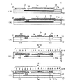
図1は本発明の一実施形態に係る電気光学装置としての液晶装置の画像形成領域を構成するマトリクス状に形成された複数の画素における各種素子、配線等の等価回路である。また、図2は、データ線、走査線、画素電極、遮光膜等が形成されたTFTアレイ基板の相隣接する複数の画素群の平面図であり、図3は、図2のA−A’断面図であり、図4は、図2のB−B’断面図である。図5は、該液晶装置における半導体層の近傍の構造を概念的に示した斜視図である。尚、図3、図4及び図5においては、各層や各部材を図面上で認識可能な程度の大きさとするため、各層や各部材毎に縮尺を異ならしめてある。また、図2及び図5おいて、X方向とは走査線と平行する方向を示し、Y方向とはデータ線と平行する方向を示す。
【0061】
図1において、本実施の形態による液晶装置の画像表示領域を構成するマトリクス状に形成された複数の画素は、マトリクス状に複数形成された画素電極9aと画素電極9aを制御するためのトランジスタとしてのTFT30からなり、画像信号が供給されるデータ線6aが当該TFT30のソースに電気的に接続されている。データ線6aに書き込む画像信号S1、S2、…、Snは、この順に線順次に供給しても構わないし、相隣接する複数のデータ線6a同士に対して、グループ毎に供給するようにしても良い。また、TFT30のゲートに走査線3aが電気的に接続されており、所定のタイミングで、走査線3aにパルス的に走査信号G1、G2、…、Gmを、この順に線順次で印加するように構成されている。画素電極9aは、TFT30のドレインに電気的に接続されており、スイッチング素子であるTFT30を一定期間だけそのスイッチを閉じることにより、データ線6aから供給される画像信号S1、S2、…、Snを所定のタイミングで書き込む。画素電極9aを介して液晶に書き込まれた所定レベルの画像信号S1、S2、…、Snは、対向基板(後述する)に形成された対向電極(後述する)との間で一定期間保持される。液晶は、印加される電圧レベルにより分子集合の配向や秩序が変化することにより、光を変調し、階調表示を可能にする。ノーマリーホワイトモードであれば、印加された電圧に応じて入射光がこの液晶部分を通過不可能とされ、ノーマリーブラックモードであれば、印加された電圧に応じて入射光がこの液晶部分を通過可能とされ、全体として液晶装置からは画像信号に応じたコントラストを持つ光が出射する。ここで、保持された画像信号がリークするのを防ぐために、画素電極9aと対向電極との間に形成される液晶容量と並列に蓄積容量70を付加する。これにより、保持特性は更に改善され、コントラスト比の高い液晶装置が実現できる。本実施の形態では特に、このような蓄積容量70を形成するために、後述の如く走査線と同層あるいは、導電性の遮光膜を利用して低抵抗化された容量線3bを設けている。
【0062】
図2において、液晶装置のTFTアレイ基板上には、マトリクス状に複数の透明な画素電極9a(一点鎖線部9a’により輪郭が示されている)が設けられており、画素電極9aの縦横の境界に各々沿ってデータ線6a、走査線3a及び容量線3bが設けられている。データ線6aは、コンタクトホール5を介して単結晶シリコン層の半導体層1aのうち後述のソース領域に電気的接続されており、画素電極9aは、コンタクトホール8を介して半導体層1aのうち後述のドレイン領域に電気的接続されている。また、半導体層1aのうちチャネル領域(後述する)に対向するように走査線3aが配置されており、走査線3aはゲート電極として機能する。
【0063】
容量線3bは、走査線3aに沿ってほぼ直線状に伸びる本線部(即ち、平面的に見て、走査線3aに沿って形成された第1領域)と、データ線6aと交差する箇所からデータ線6aに沿って前段側(図中、上向き)に突出した突出部(即ち、平面的に見て、データ線6aに沿って延設された第2領域)とを有する。
【0064】
そして、図中右上がりの斜線で示した領域には、複数の第1遮光膜11aが設けられている。より具体的には、第1遮光膜11aは夫々、画素部において半導体層1aのチャネル領域を含むTFTをTFTアレイ基板の側から見て覆う位置に設けられており、更に、容量線3bの本線部に対向して走査線3aに沿って直線状に伸びる本線部と、データ線6aと交差する箇所からデータ線6aに沿って隣接する段側(即ち、図中下向き)に突出した突出部とを有する。第1遮光膜11aの各段(画素行)における下向きの突出部の先端は、データ線6a下において次段における容量線3bの上向きの突出部の先端と重ねられている。この重なった箇所には、第1遮光膜11aと容量線3bとを相互に電気的接続するコンタクトホール13が設けられている。即ち、本実施の形態では、第1遮光膜11aは、コンタクトホール13により前段あるいは後段の容量線3bに電気的接続されている。
【0065】
次に、図3の断面図に示すように、液晶装置は、光透過性基板の一例を構成するTFTアレイ基板10と、これに対向配置される透明な対向基板20とを備えている。TFTアレイ基板10は、例えば石英基板からなり、対向基板20は、例えばガラス基板や石英基板からなる。TFTアレイ基板10には、画素電極9aが設けられており、その上側には、ラビング処理等の所定の配向処理が施された配向膜16が設けられている。画素電極9aは例えば、ITO膜(インジウム・ティン・オキサイド膜)などの透明導電性薄膜からなる。また配向膜16は例えば、ポリイミド薄膜などの有機薄膜からなる。
【0066】
他方、対向基板20には、その全面に渡って対向電極(共通電極)21が設けられており、その下側には、ラビング処理等の所定の配向処理が施された配向膜22が設けられている。対向電極21は例えば、ITO膜などの透明導電性薄膜からなる。また配向膜22は、ポリイミド薄膜などの有機薄膜からなる。
【0067】
TFTアレイ基板10には、図3に示すように、各画素電極9aに隣接する位置に、各画素電極9aをスイッチング制御する画素スイッチング用TFT30が設けられている。
【0068】
対向基板20には、更に図3に示すように、各画素部の開口領域以外の領域に第2遮光膜23が設けられている。このため、対向基板20の側から入射光が画素スイッチング用TFT30の半導体層1aのチャネル領域1a’やLDD(Lightly Doped Drain)領域1b及び1cに侵入することはない。更に、第2遮光膜23は、コントラストの向上、色材の混色防止などの機能を有する。
【0069】
このように構成され、画素電極9aと対向電極21とが対面するように配置されたTFTアレイ基板10と対向基板20との間には、シール材(図示を省略)により囲まれた空間に液晶が封入され、液晶層50が形成される。液晶層50は、画素電極9aからの電界が印加されていない状態で配向膜16及び22により所定の配向状態を採る。液晶層50は、例えば一種又は数種類のネマティック液晶を混合した液晶からなる。シール材は、二つの基板10及び20をそれらの周辺で貼り合わせるための、例えば光硬化性樹脂や熱硬化性樹脂からなる接着剤であり、両基板間の距離を所定値とするためのグラスファイバー或いはガラスビーズ等のスペーサが混入されている。
【0070】
図3に示すように、画素スイッチング用TFT30に各々対向する位置においてTFTアレイ基板10表面の各画素スイッチング用TFT30に対応する位置には第1遮光膜11aが各々設けられている。ここで、第1遮光膜11aは、好ましくは不透明な高融点金属であるTi、Cr、W、Ta、Mo及びPdのうちの少なくとも一つを含む、金属単体、合金、金属シリサイド等から構成される。このような材料から構成すれば、TFTアレイ基板10上の第1遮光膜11aの形成工程の後に行われる画素スイッチング用TFT30の形成工程における高温処理により、第1遮光膜11aが破壊されたり溶融しないようにできる。第1遮光膜11aが形成されているので、TFTアレイ基板10の側からの戻り光等が画素スイッチング用TFT30のチャネル領域1a’やLDD領域1b、1cに入射する事態を未然に防ぐことができ、光電流の発生によりトランジスタ素子としての画素スイッチング用TFT30の特性が劣化することはない。
【0071】
更に、第1遮光膜11aと複数の画素スイッチング用TFT30との間には、第1層間絶縁膜12が設けられている。第1層間絶縁膜12は、画素スイッチング用TFT30を構成する半導体層1aを第1遮光膜11aから電気的絶縁するために設けられるものである。更に、第1層間絶縁膜12は、TFTアレイ基板10の全面に形成されることにより、画素スイッチング用TFT30のための下地膜としての機能をも有する。即ち、TFTアレイ基板10の表面の研磨時における荒れや、洗浄後に残る汚れ等で画素スイッチング用TFT30の特性の劣化を防止する機能を有する。第1層間絶縁膜12は、例えば、NSG(ノンドープトシリケートガラス)、PSG(リンシリケートガラス)、BSG(ボロンシリケートガラス)、BPSG(ボロンリンシリケートガラス)などの高絶縁性ガラス又は、酸化シリコン膜、窒化シリコン膜等からなる。第1層間絶縁膜12により、第1遮光膜11aが画素スイッチング用TFT30等を汚染する事態を未然に防ぐこともできる。
【0072】
本実施の形態では、ゲート絶縁膜2を走査線3aに対向する位置から延設して誘電体膜として用い、半導体膜1aを延設して第1蓄積容量電極1fとし、更にこれらに対向する容量線3bの一部を第2蓄積容量電極とすることにより、蓄積容量70が構成されている。より詳細には、半導体層1aの高濃度ドレイン領域1eが、データ線6a及び走査線3aに沿って伸びる容量線3b部分に絶縁膜2を介して対向配置されて、第1蓄積容量電極(半導体層)1fとされている。特に蓄積容量70の誘電体としての絶縁膜2は、高温酸化により単結晶シリコン層上に形成されるTFT30のゲート絶縁膜2に他ならないので、薄く且つ高耐圧の絶縁膜とすることができ、蓄積容量70は比較的小面積で大容量の蓄積容量として構成できる。
【0073】
更に、蓄積容量70においては、図2及び図3から分かるように、第1遮光膜11aは、第2蓄積容量電極としての容量線3bの反対側において第1蓄積容量電極1fに第1層間絶縁膜12を介して第3蓄積容量電極として対向配置されることにより(図3の右側の蓄積容量70参照)、蓄積容量が更に付与されるように構成されている。即ち、本実施の形態では、第1蓄積容量電極1fを挟んで両側に蓄積容量が付与されるダブル蓄積容量構造が構築されており、蓄積容量がより増加する。よって、当該液晶装置が持つ、表示画像におけるフリッカや焼き付きを防止する機能が向上する。
【0074】
これらの結果、データ線6a下の領域及び走査線3aに沿って液晶のディスクリネーションが発生する領域(即ち、容量線3bが形成された領域)という開口領域を外れたスペースを有効に利用して、画素電極9aの蓄積容量を増やすことが出来る。
【0075】
また、第1遮光膜11a(及びこれに電気的接続された容量線3b)は定電位源に電気的接続されており、第1遮光膜11a及び容量線3bは、定電位とされる。従って、第1遮光膜11aに対向配置される画素スイッチング用TFT30に対し第1遮光膜11aの電位変動が悪影響を及ぼすことはない。また、容量線3bは、蓄積容量70の第2蓄積容量電極として良好に機能し得る。この場合、定電位源としては、当該液晶装置を駆動するための周辺回路(例えば、走査線駆動回路、データ線駆動回路等)に供給される負電源、正電源等の定電位源、接地電源、対向電極21に供給される定電位源等が挙げられる。このように周辺回路等の電源を利用すれば、専用の電位配線や外部入力端子を設ける必要なく、遮光膜11a及び容量線3bを定電位にできる。
【0076】
更に、図2及び図3に示したように、コンタクトホール13を介して第1遮光膜11aは、前段あるいは後段の容量線3bに電気的接続するように構成されている。従って、各第1遮光膜11aが、自段の容量線に電気的接続される場合と比較して、画素部の開口領域の縁に沿って、データ線6aに重ねて容量線3b及び第1遮光膜11aが形成される領域の他の領域に対する段差が少なくて済む。このように画素部の開口領域の縁に沿った段差が少ないと、当該段差に応じて引き起こされる液晶のディスクリネーション(配向不良)を低減できるので、画素部の開口領域を広げることが可能となる。
【0077】
また、第1遮光膜11aは、前述のように直線状に伸びる本線部から突出した突出部にコンタクトホール13が開孔されている。ここで、コンタクトホール13の開孔箇所としては、縁に近い程、ストレスが縁から発散される等の理由により、クラックが生じ難いことが判明されている。従ってこの場合、どれだけ突出部の先端に近づけてコンタクトホール13を開孔するかに応じて(好ましくは、マージンぎりぎりまで先端に近づけるかに応じて)、製造プロセス中に第1遮光膜11aにかかる応力が緩和されて、より効果的にクラックを防止し得、歩留まりを向上させることが可能となる。
【0078】
更に、図2、図4及び図5に示すように、半導体層1aのチャネル領域1a窒ノは、X方向(半導体層1aのソース領域、チャネル領域及びドレイン領域と並ぶ方向をY方向とし、基板10平面上でY方向と直交する方向をX方向とする。)に向けて延在する延在部201を有する。この結果、延在部201は走査線3aと対向するように延在している。延在部201の終端部は、第2層間絶縁膜4に形成されたコンタクトホール202を介して接続配線203に接続されている。接続配線203は、一端が上記のようにコンタクトホール202を介して延在部201に接続されると共に、Y方向に向けて容量線3bの直上まで配設され、該直上よりコンタクトホール204を介して容量線3bに接続されている。これにより、半導体層1aのチャネル領域1a窒ヘ上述した定電位源に接続された容量線3bの電位に固定され、SOI構造に起因する基板浮遊効果によってトランジスタ素子のソース・ドレイン耐圧が劣化するなどの問題が解消され、素子の電気的特性を安定化させることができる。
【0079】
また、走査線3aと容量線3bは第1層間絶縁膜12と第2層間絶縁膜4との間に層上に互いに隣接するように並設され、更に延在部201が走査線3aと対向するように延在しているているため、走査線3aとコンタクトホール202とが配置上干渉する。そこで、本実施形態では、特に走査線3aがコンタクトホール202を回避するように形成された回り込み部3a’を有する。
【0080】
また、容量線3bと走査線3aとは、同一のポリシリコン膜からなり、蓄積容量70の誘電体膜とTFT30のゲート絶縁膜2とは、同一の高温酸化膜からなり、第1蓄積容量電極1fと、TFT30のチャネル形成領域1a’、ソース領域1d、ドレイン領域1e、延在部201等とは、同一の半導体層1aからなり、
データ線6aと接続配線203とは同一の金属膜からなる。このため、TFTアレイ基板10上に形成される積層構造を単純化でき、更に、後述の液晶装置の製造方法において、同一の薄膜形成工程で容量線3b及び走査線3aを同時に形成でき、蓄積容量70の誘電体膜及びゲート絶縁膜2等を同時に形成できる。
【0081】
更に、第1遮光膜11aは、走査線3aに沿って夫々伸延しており、しかも、データ線6aに沿った方向に対し複数の縞状に分断されている。このため、例えば各画素部の開口領域の周りに一体的に形成された格子状の遮光膜を配設した場合と比較して、第1遮光膜11a、走査線3a及び容量線3bを形成するポリシリコン膜、データ線6aを形成する金属膜、層間絶縁膜等からなる当該液晶装置の積層構造において、各膜の物性の違いに起因した製造プロセス中の加熱冷却に伴い発生するストレスが格段に緩和される。このため、第1遮光膜11a等におけるクラックの発生防止や歩留まりの向上が図られる。
【0082】
尚、図2では、第1遮光膜11aにおける直線状の本線部分は、容量線3bの直線状の本線部分にほぼ重ねられるように形成されているが、第1遮光膜11aが、TFT30のチャネル領域を覆う位置に設けられており且つコンタクトホール13を形成可能なように容量線3bと何れかの箇所で重ねられていれば、TFTに対する遮光機能及び容量線に対する低抵抗化機能を発揮可能である。従って、例えば相隣接した走査線3aと容量線3bとの間にある走査線に沿った長手状の間隙領域や、走査線3aと若干重なる位置にまでも、当該第1遮光膜11aを設けてもよい。
【0083】
容量線3bと第1遮光膜11aとは、第1層間絶縁膜12に開孔されたコンタクトホール13を介して確実に且つ高い信頼性を持って、両者は電気的接続されているが、このようなコンタクトホール13は、画素毎に開孔されても良く、複数の画素からなる画素グループ毎に開孔されても良い。
【0084】
コンタクトホール13を画素毎に開孔した場合には、第1遮光膜11aによる容量線3bの低抵抗化を促進でき、更に、両者間における冗長構造の度合いを高められる。他方、コンタクトホール13を複数の画素からなる画素グループ毎に(例えば2画素毎に或いは3画素毎に)開孔した場合には、容量線3bや第1遮光膜11aのシート抵抗、駆動周波数、要求される仕様等を勘案しつつ、第1遮光膜11aによる容量線3bの低抵抗化及び冗長構造による利益と、多数のコンタクトホール13を開孔することによる製造工程の複雑化或いは当該液晶装置の不良化等の弊害とを適度にバランスできるので、実践上大変有利である。
【0085】
また、このような画素毎或いは画素グループ毎に設けられるコンタクトホール13は、対向基板20の側から見てデータ線6aの下に開孔されている。このため、コンタクトホール13は、画素部の開口領域から外れており、しかもTFT30や第1蓄積容量電極1fが形成されていない第1層間絶縁膜12の部分に設けられているので、画素領域の有効利用を図りつつ、コンタクトホール13の形成によるTFT30や他の配線等の不良化を防ぐことができる。
【0086】
再び、図3において、画素スイッチング用TFT30は、LDD(Lightly Doped Drain)構造を有しており、走査線3a、該走査線3aからの電界によりチャネルが形成される半導体層1aのチャネル領域1a’走査線3aと半導体層1aとを絶縁するゲート絶縁膜2、データ線6a、半導体層1aの低濃度ソース領域(ソース側LDD領域)1b及び低濃度ドレイン領域(ドレイン側LDD領域)1c、半導体層1aの高濃度ソース領域1d並びに高濃度ドレイン領域1eを備えている。高濃度ドレイン領域1eには、複数の画素電極9aのうちの対応する一つが接続されている。ソース領域1b及び1d並びにドレイン領域1c及び1eは後述のように、半導体層1aに対し、n型又はp型のチャネルを形成するかに応じて所定濃度のn型用又はp型用のドーパントをドープすることにより形成されている。n型チャネルのTFTは、動作速度が速いという利点があり、画素のスイッチング素子である画素スイッチング用TFT30として用いられることが多い。データ線6aは、Al等の金属膜や金属シリサイド等の合金膜などの遮光性の薄膜から構成されている。また、走査線3a、ゲート絶縁膜2及び第1層間絶縁膜12の上には、高濃度ソース領域1dへ通じるコンタクトホール5及び高濃度ドレイン領域1eへ通じるコンタクトホール8が各々形成された第2層間絶縁膜4が形成されている。このソース領域1bへのコンタクトホール5を介して、データ線6aは高濃度ソース領域1dに電気的接続されている。更に、データ線6a及び第2層間絶縁膜4の上には、高濃度ドレイン領域1eへのコンタクトホール8が形成された第3層間絶縁膜7が形成されている。この高濃度ドレイン領域1eへのコンタクトホール8を介して、画素電極9aは高濃度ドレイン領域1eに電気的接続されている。前述の画素電極9aは、このように構成された第3層間絶縁膜7の上面に設けられている。尚、画素電極9aと高濃度ドレイン領域1eとは、データ線6aと同一のAl膜や走査線3bと同一のポリシリコン膜を中継しての電気的接続するようにしてもよい。
【0087】
画素スイッチング用TFT30は、好ましくは上述のようにLDD構造を持つが、低濃度ソース領域1b及び低濃度ドレイン領域1cに不純物イオンの打ち込みを行わないオフセット構造を持ってよいし、ゲート電極3aをマスクとして高濃度で不純物イオンを打ち込み、自己整合的に高濃度ソース及びドレイン領域を形成するセルフアライン型のTFTであってもよい。
【0088】
また、画素スイッチング用TFT30のゲート電極(走査線3a)をソース−ドレイン領域1b及び1e間に1個のみ配置したシングルゲート構造としたが、これらの間に2個以上のゲート電極を配置してもよい。この際、各々のゲート電極には同一の信号が印加されるようにする。このようにダブルゲート或いはトリプルゲート以上でTFTを構成すれば、チャネルとソース−ドレイン領域接合部のリーク電流を防止でき、オフ時の電流を低減することができる。これらのゲート電極の少なくとも1個をLDD構造或いはオフセット構造にすれば、更にオフ電流を低減でき、安定したスイッチング素子を得ることができる。
【0089】
ここで、一般には、半導体層1aのチャネル領域1a’、低濃度ソース領域1b及び低濃度ドレイン領域1c等の単結晶シリコン層は、光が入射するとシリコンが有する光電変換効果により光電流が発生してしまい画素スイッチング用TFT30のトランジスタ特性が劣化するが、本実施の形態では、走査線3aを上側から覆うようにデータ線6aがAl等の遮光性の金属薄膜から形成されているので、少なくとも半導体層1aのチャネル領域1a’及びLDD領域1b、1cへの入射光の入射を効果的に防ぐことが出来る。また、前述のように、画素スイッチング用TFT30の下側には、第1遮光膜11aが設けられているので、少なくとも半導体層1aのチャネル領域1a’及びLDD領域1b、1cへの戻り光の入射を効果的に防ぐことが出来る。
【0090】
尚、この実施形態では、相隣接する前段あるいは後段の画素に設けられた容量線3bと第1遮光膜11aとを接続しているため、最上段あるいは最下段の画素に対して第1遮光膜11aに定電位を供給するための容量線3bが必要となる。そこで、容量線3bの数を垂直画素数に対して1本余分に設けておくようにすると良い。
【0091】
尚、図22に図5の実施形態においてTFTアレイ基板と対向基板を液晶を介在させて構成した液晶装置の等価回路図を示す。図22に示されるように、データ線6a(S1,S2…)と走査線3a(G1,G2…)とがマトリクス平面上に配設され、この平面上の交差点近傍には画素スイッチング用TFT30がそれぞれ配置される。画素スイッチング用TFT30のソースはデータ線6aに接続され、ゲート電極は走査線3aに接続されており、ドレインは画素電極9aに接続されている。さらに画素電極9aは対向基板内面に配置された対向電極21と液晶層を挟んで対向し、両電極間の液晶を極性反転駆動する。尚、ソースとドレインとは入れ替えてもよい。対向電極21には極性反転駆動の基準電位となる共通電位VLCが印加され、画素電極9aと対向電極21とは液晶層を誘電体とする液晶容量CLCを構成する。また、容量電極1fは容量線3bとの間に保持容量(蓄積容量)Csを構成する。すなわち、一画素は、画素スイッチング用TFTとそれに接続された液晶容量と保持容量により構成される。
【0092】
トランジスタのチャネル領域1aは、このトランジスタを駆動する容量線3bと電気的に接続される。このように各トランジスタのチャネル領域はそのトランジスタに接続される容量の一方の電極である容量線3bに電気的に接続され、チャネル領域1aから蓄積された余剰キャリアを容量線3bに引き抜くことにより基板浮遊効果を抑制する。尚、容量線3bには、共通電極電位VLCが印加される。
【0093】
(電気光学装置の製造方法)
次に、以上のような構成を持つ液晶装置の製造プロセスについて、図6から図11を参照して説明する。
【0094】
尚、図6から図11は各工程におけるTFTアレイ基板側の各層を、図3と同様に図2のA−A’断面に対応させて示す工程図である。
【0095】
図6の工程(1)に示すように、石英基板、ハードガラス等のTFTアレイ基板10を用意する。ここで、好ましくはN2(窒素)等の不活性ガス雰囲気且つ約900〜1300℃の高温でアニール処理し、後に実施される高温プロセスにおけるTFTアレイ基板10に生じる歪みが少なくなるように前処理しておく。即ち、製造プロセスにおける最高温で高温処理される温度に合わせて、事前にTFTアレイ基板10を同じ温度かそれ以上の温度で熱処理しておく。
【0096】
このように処理されたTFTアレイ基板10の全面に、Ti、Cr、W、Ta、Mo及びPd等の金属や金属シリサイド等の金属合金膜を、スパッタにより、200〜400nm程度の層厚、好ましくは約200nmの層厚の遮光膜11を形成する。
【0097】
続いて、工程(2)に示すように、該形成された遮光膜11上にフォトリソグラフィにより第1遮光膜11aのパターン(図2参照)に対応するレジストマスクを形成し、該レジストマスクを介して遮光膜11に対しエッチングを行うことにより、第1遮光膜11aを形成する。
【0098】
次に、工程(3)に示すように、第1遮光膜11aの上に、例えば、常圧又は減圧CVD法等によりTEOS(テトラ・エチル・オルソ・シリケート)ガス、TEB(テトラ・エチル・ボートレート)ガス、TMOP(テトラ・メチル・オキシ・フォスレート)ガス等を用いて、NSG、PSG、BSG、BPSGなどのシリケートガラス膜、窒化シリコン膜や酸化シリコン膜等からなる第1層間絶縁膜12を形成する。この第1層間絶縁膜12の層厚は、例えば、約600〜1000nm、より好ましくは800nm程度とする。
【0099】
次に、工程(4)に示すように、第1層間絶縁膜12の表面を、グローバルに研磨して平坦化する。研磨による平坦化の手法としては、例えばCMP(化学的機械研磨)法を用いることができる。
【0100】
次に、工程(5)に示すように、基板10と単結晶シリコン基板206aとの貼り合わせを行う。貼り合わせに用いる単結晶シリコン基板206aは、厚さ600μmであり、その表面をあらかじめ0.05〜0.8μm程度酸化し、酸化膜層206bを形成すると共に、水素イオン(H+)を例えば加速電圧100keV、ドーズ量10e16/cm2にて注入したものである。貼り合わせ工程は、例えば300℃で2時間の熱処理によって2枚の基板を直接貼り合わせる方法が採用できる。
【0101】
次に、工程(6)に示すように、貼り合わせた単結晶シリコン基板206aの貼り合わせ面側の酸化膜206bと単結晶シリコン層206を残したまま、単結晶シリコン基板206aを基板10から剥離するための熱処理を行う。この基板の剥離現象は、単結晶シリコン基板中に導入された水素イオンによって、単結晶シリコン基板の表面近傍のある層でシリコンの結合が分断されるために生じるものである。例えば、貼り合わせた2枚の基板を毎分20℃の昇温速度にて600℃まで加熱することにより行うことができる。この熱処理によって、貼り合わせた単結晶シリコン基板206aが基板10と分離し、基板10表面には約200nm±5nm程度の単結晶シリコン層206が形成される。なお、基板10上に貼り合わされる単結晶シリコン層206は、前に述べた単結晶シリコン基板に対して行われる水素イオン注入の加速電圧を変えることによって任意の膜厚で形成することが可能である。
【0102】
次に、工程(7)に示すように、フォトリソグラフィ工程、エッチング工程等により、図2に示した如き所定パターンの半導体層1aを形成する。即ち、特にデータ線6a下で容量線3bが形成される領域及び走査線3aに沿って容量線3bが形成される領域には、画素スイッチング用TFT30を構成する半導体層1aから延設された第1蓄積容量電極1fを形成する。また、同時に半導体層1aのチャネル領域1a’から延在する延在部201も形成する。
【0103】
次に、工程(8)に示すように、画素スイッチング用TFT30を構成する半導体層1aと共に第1蓄積容量電極1fを約850〜1300℃の温度、好ましくは約1000℃の温度で72分程度熱酸化することにより、約60nmの比較的薄い厚さの熱酸化シリコン膜を形成し、画素スイッチング用TFT30のゲート絶縁膜2と共に容量形成用のゲート絶縁膜2を形成する。この結果、半導体層1a及び第1蓄積容量電極1fの厚さは、約170nmの厚さ、ゲート絶縁膜2の厚さは、約60nmの厚さとなる。
【0104】
次に、図7の工程(9)に示すように、Nチャネルの半導体層1aに対応する位置にレジスト膜301を形成し、Pチャネルの半導体層1aにPなどのV族元素のドーパント302を低濃度で(例えば、Pイオンを70keVの加速電圧、2e11/cm2のドーズ量にて)ドープする。
【0105】
次に、工程(10)に示すように、図示を省略するPチャネルの半導体層1aに対応する位置にレジスト膜を形成し、Nチャネルの半導体層1aにBなどのIII族元素のドーパント303を低濃度で(例えば、Bイオンを35keVの加速電圧、1e12/cm2のドーズ量にて)ドープする。
【0106】
ここで、図17及び図18のグラフに示すように、ドーパンドの種類及びドーズ量によって、更には工程の順番によって各チャネルのしきい値電圧Vthを制御することが可能である。
【0107】
図17はPチャネルにおけるドーズ量としきい値電圧Vthとの関係を示している。図17▲1▼はドーパンドとしてボロンを用いた場合のシミュレーション結果、図17▲2▼はドーパンドとしてリンを用いた場合のシミュレーション結果、図17▲3▼は実験結果を示している。これらの図から分かるように、しきい値電圧Vthとして−1.5Vを得たい場合にはリンを1e12/cm2のドーズ量でドープするのが好適である。
【0108】
図18はNチャネルにおけるドーズ量としきい値電圧Vthとの関係を示している。図18▲1▼はドーパンドとしてボロンを用いた場合のシミュレーション結果、図18▲2▼は工程(8)の後に工程(9)及び工程(10)を行った場合の実験結果、図18▲3▼は工程(9)及び工程(10)の後に工程(8)を行った場合の実験結果を示している。これらの図から分かるように、しきい値電圧Vthとして1.5Vを得たい場合にはボロンを7e11/cm2のドーズ量でドープするのが好適である。
【0109】
次に、工程(11)に示すように、Pチャネル、Nチャネル毎に各半導体層1aのチャネル領域1a’の端部304(図12及び図13参照)を除く基板10の表面にレジスト膜305を形成し、端部304にPチャネルについて工程(9)の約1〜10倍のドーズ量のPなどのV族元素のドーパント306、Nチャネルについて工程(10)の約1〜10倍のドーズ量のBなどのIII族元素のドーパント306をドープする。半導体層1aのチャネル領域1a窒フ端部304は電界が集中して見かけ上のしきい値電圧が低くなり、リーク電流が流れようとするが、かかるドープ工程により半導体層1aのチャネル領域1a’の端部304が、チャネル領域1a窒フ不純物濃度が他の部分に比べより高くなっているので、この領域における見かけ上のしきい値電圧は高くなり、前述のように電界が集中してもリーク電流が流れるのを防ぐことができる。
【0110】
次に、工程(12)に示すように、半導体膜1aを延設してなる第1蓄積容量電極1fを低抵抗化するため、基板10の表面の走査線3a(ゲート電極)に対応する部分にレジスト膜307(走査線3aよりも幅が広い)を形成し、これをマスクとしてその上からPなどのV族元素のドーパント308を低濃度で(例えば、Pイオンを70keVの加速電圧、3e14/cm2のドーズ量にて)ドープする。
【0111】
次に、図8の工程(13)に示すように、第1層間絶縁膜12に第1遮光膜11aに至るコンタクトホール13を反応性エッチング、反応性イオンビームエッチング等のドライエッチングにより或いはウエットエッチングにより形成する。この際、反応性エッチング、反応性イオンビームエッチングのような異方性エッチングにより、コンタクトホール13等を開孔した方が、開孔形状をマスク形状とほぼ同じにできるという利点がある。但し、ドライエッチングとウエットエッチングとを組み合わせて開孔すれば、これらのコンタクトホール13等をテーパ状にできるので、配線接続時の断線を防止できるという利点が得られる。
【0112】
次に、工程(14)に示すように、減圧CVD法等によりポリシリコン層3を350nm〜550nmの厚さで堆積した後、リン(P)を熱拡散し、ポリシリコン膜3を導電化する。又は、Pイオンをポリシリコン膜3の成膜と同時に導入したドープトシリコン膜を用いてもよい。これにより、ポリシリコン層3の導電性を高めることができる。そして、走査線のゲート電極領域の厚さが350nmより大きいことで、配線抵抗を低減し、配線遅延による画素への信号書き込み速度の低下を十分に抑えることができる。また、走査線のゲート電極領域の厚さが550nmより小さいことで、このゲート電極の膜厚に起因する素子基板の段差を必要最小限に抑えることができ、この結果液晶を配向させた際のディスクリネーションを抑制し表示画質を良好に保つことができる。なお、ポリシリコン層3に加えて導電性金属層を積層することでも導電性を高めることができる。
【0113】
次に、工程(15)に示すように、レジストマスクを用いたフォトリソグラフィ工程、エッチング工程等により、図2に示した如き所定パターンの走査線3aと共に容量線3bを形成する。尚、この後、基板10の裏面に残存するポリシリコンを基板10の表面をレジスト膜で覆ってエッチングにより除去する。
【0114】
次に、工程(16)に示すように、半導体層1aにPチャネルのLDD領域を形成するために、Nチャネルの半導体層1aに対応する位置をレジスト膜309で覆い(図はNチャネルの半導体層1aを示している。)、走査線3a(ゲート電極)を拡散マスクとして、まずBなどのIII族元素のドーパント310を低濃度で(例えば、BF2イオンを90keVの加速電圧、3e13/cm2のドーズ量にて)ドープし、Pチャネルの低濃度ソース領域1b及び低濃度ドレイン領域1cを形成する。
【0115】
続いて、工程(17)に示すように、半導体層1aにPチャネルの高濃度ソース領域1d及び高濃度ドレイン領域1eを形成するために、Nチャネルの半導体層1aに対応する位置をレジスト膜309で覆った状態で、かつ、図示はしていないが走査線3aよりも幅の広いマスクでレジスト層をPチャネルに対応する走査線3a上に形成した状態、同じくBなどのIII族元素のドーパント311を高濃度で(例えば、BF2イオンを90keVの加速電圧、2e15/cm2のドーズ量にて)ドープする。
【0116】
次に、図9の工程(18)に示すように、半導体層1aにNチャネルのLDD領域を形成するために、Pチャネルの半導体層1aに対応する位置をレジスト膜(図示せず)で覆い、走査線3a(ゲート電極)を拡散マスクとして、PなどのV族元素のドーパント60を低濃度で(例えば、Pイオンを70keVの加速電圧、6e12/cm2のドーズ量にて)ドープし、Nチャネルの低濃度ソース領域1b及び低濃度ドレイン領域1cを形成するする。
【0117】
続いて、工程(19)に示すように、半導体層1aにNチャネルの高濃度ソース領域1d及び高濃度ドレイン領域1eを形成するために、走査線3aよりも幅の広いマスクでレジスト層62をNチャネルに対応する走査線3a上に形成した後、同じくPなどのV族元素のドーパント61を高濃度で(例えば、Pイオンを70keVの加速電圧、4e15/cm2のドーズ量にて)ドープする。
【0118】
ここで、図19にLDD領域を3e13/cm2のドーズ量のドーパント311でドープして形成されたPチャネルの半導体層1aの電圧−電流特性を示す。また、図20にLDD領域を1e13/cm2のドーズ量のドーパント61でドープして形成されたNチャネルの半導体層1aの電圧−電流特性を示す。更に、図21にLDD領域を6e12/cm2のドーズ量のドーパント61でドープして形成されたNチャネルの半導体層1aの電圧−電流特性を示す。
【0119】
次に、工程(20)に示すように、画素スイッチング用TFT30における走査線3aと共に容量線3b及び走査線3aを覆うように、例えば、常圧又は減圧CVD法やTEOSガス等を用いて、NSG、PSG、BSG、BPSGなどのシリケートガラス膜、窒化シリコン膜や酸化シリコン膜等からなる第2層間絶縁膜4を形成する。第2層間絶縁膜4の層厚は、約600〜1500nmが好ましく、更に800nmがより好ましい。
【0120】
この後、高濃度ソース領域1d及び高濃度ドレイン領域1eを活性化するために約850℃のアニール処理を20分程度行う。
【0121】
次に、工程(21)に示すように、データ線6aを形成するためのコンタクトホール5及びコンタクトホール202、204(図4及び図5参照)を、反応性イオンエッチング、反応性イオンビームエッチング等のドライエッチングにより或いはウエットエッチングにより形成する。また、走査線3aや容量線3bを図示しない配線と接続するためのコンタクトホールも、コンタクトホール5と同一の工程により第2層間絶縁膜4に開孔する。
【0122】
次に、図10の工程(22)に示すように、第2層間絶縁膜4の上に、スパッタ処理等により、遮光性のAl等の低抵抗金属や金属シリサイド等を金属膜6として、約100〜700nmの厚さ、好ましくは約350nmに堆積し、更に工程(23)に示すように、フォトリソグラフィ工程、エッチング工程等により、データ線6aを形成する。このとき同時に金属膜6により接続配線203も形成する(図4及び図5参照)。
【0123】
次に、工程(24)に示すように、データ線6a上を覆うように、例えば、常圧又は減圧CVD法やTEOSガス等を用いて、NSG、PSG、BSG、BPSGなどのシリケートガラス膜、窒化シリコン膜や酸化シリコン膜等からなる第3層間絶縁膜7を形成する。第3層間絶縁膜7の層厚は、約600〜1500nmが好ましく、更に800nmがより好ましい。
【0124】
次に、図11の工程(25)に示すように、画素スイッチング用TFT30において、画素電極9aと高濃度ドレイン領域1eとを電気的接続するためのコンタクトホール8を、反応性イオンエッチング、反応性イオンビームエッチング等のドライエッチングにより形成する。
【0125】
次に、工程(26)に示すように、第3層間絶縁膜7の上に、スパッタ処理等により、ITO膜等の透明導電性薄膜9を、約50〜200nmの厚さに堆積し、更に工程(27)に示すように、フォトリソグラフィ工程、エッチング工程等により、画素電極9aを形成する。尚、当該液晶装置を反射型の液晶装置に用いる場合には、Al等の反射率の高い不透明な材料により画素電極9aを形成してもよい。
【0126】
続いて、画素電極9aの上にポリイミド系の配向膜の塗布液を塗布した後、所定のプレティルト角を持つように且つ所定方向でラビング処理を施すこと等により、配向膜16(図3参照)が形成される。
【0127】
他方、図3及び図4に示した対向基板20については、ガラス基板等が先ず用意され、第2遮光膜23及び後述の額縁としての第2遮光膜が、例えば金属クロムをスパッタした後、フォトリソグラフィ工程、エッチング工程を経て形成される。尚、これらの第2遮光膜は、Cr、Ni、Alなどの金属材料の他、カーボンやTiをフォトレジストに分散した樹脂ブラックなどの材料から形成してもよい。
【0128】
その後、対向基板20の全面にスパッタ処理等により、ITO等の透明導電性薄膜を、約50〜200nmの厚さに堆積することにより、対向電極21を形成する。更に、対向電極21の全面にポリイミド系の配向膜の塗布液を塗布した後、所定のプレティルト角を持つように且つ所定方向でラビング処理を施すこと等により、配向膜22(図3参照)が形成される。
【0129】
最後に、上述のように各層が形成されたTFTアレイ基板10と対向基板20とは、配向膜16及び22が対面するようにシール材52により貼り合わされ、真空吸引等により、両基板間の空間に、例えば複数種類のネマティック液晶を混合してなる液晶が吸引されて、所定層厚の液晶層50が形成される。
【0130】
(液晶装置の全体構成)
以上のように構成された液晶装置の各実施の形態の全体構成を図14及び図15を参照して説明する。尚、図14は、TFTアレイ基板10をその上に形成された各構成要素と共に対向基板20の側から見た平面図であり、図15は、対向基板20を含めて示す図14のH−H’断面図である。
【0131】
図14において、TFTアレイ基板10の上には、シール材52がその縁に沿って設けられており、その内側に並行して、例えば第2遮光膜23と同じ或いは異なる材料から成る額縁としての第2遮光膜53が設けられている。シール材52の外側の領域には、データ線駆動回路101及び実装端子102がTFTアレイ基板10の一辺に沿って設けられており、走査線駆動回路104が、この一辺に隣接する2辺に沿って設けられている。走査線3aに供給される走査信号遅延が問題にならないのならば、走査線駆動回路104は片側だけでも良いことは言うまでもない。また、データ線駆動回路101を画面表示領域の辺に沿って両側に配列してもよい。例えば奇数列のデータ線6aは画面表示領域の一方の辺に沿って配設されたデータ線駆動回路から画像信号を供給し、偶数列のデータ線は前記画面表示領域の反対側の辺に沿って配設されたデータ線駆動回路から画像信号を供給するようにしてもよい。この様にデータ線6aを櫛歯状に駆動するようにすれば、データ線駆動回路の占有面積を拡張することができるため、複雑な回路を構成することが可能となる。更にTFTアレイ基板10の残る一辺には、画面表示領域の両側に設けられた走査線駆動回路104間をつなぐための複数の配線105が設けられている。また、対向基板20のコーナー部の少なくとも1箇所においては、TFTアレイ基板10と対向基板20との間で電気的導通をとるための導通材106が設けられている。そして、図15に示すように、図13に示したシール材52とほぼ同じ輪郭を持つ対向基板20が当該シール材52によりTFTアレイ基板10に固着されている。
【0132】
以上の液晶装置のTFTアレイ基板10上には更に、製造途中や出荷時の当該液晶装置の品質、欠陥等を検査するための検査回路等を形成してもよい。また、データ線駆動回路101及び走査線駆動回路104をTFTアレイ基板10の上に設ける代わりに、例えばTAB(テープオートメイテッドボンディング基板)上に実装された駆動用LSIに、TFTアレイ基板10の周辺部に設けられた異方性導電フィルムを介して電気的及び機械的に接続するようにしてもよい。また、対向基板20の投射光が入射する側及びTFTアレイ基板10の出射光が出射する側には各々、例えば、TN(ツイステッドネマティック)モード、STN(スーパーTN)モード、D−STN(デュアルスキャン−STN)モード等の動作モードや、ノーマリーホワイトモード/ノーマリーブラックモードの別に応じて、偏光フィルム、位相差フィルム、偏光手段などが所定の方向で配置される。
【0133】
以上説明した液晶装置は、例えばカラー液晶プロジェクタ(投射型表示装置)に適用される場合には、3枚の液晶装置がRGB用のライトバルブとして各々用いられ、各パネルには各々RGB色分解用のダイクロイックミラーを介して分解された各色の光が投射光として各々入射されることになる。従って、その場合には上記実施の形態で示したように、対向基板20に、カラーフィルタは設けられていない。しかしながら、第2遮光膜23の形成されていない画素電極9aに対向する所定領域にRGBのカラーフィルタをその保護膜と共に、対向基板20上に形成してもよい。このようにすれば、液晶プロジェクタ以外の直視型や反射型のカラー液晶テレビなどのカラー液晶装置に各実施の形態における液晶装置を適用できる。更に、対向基板20上に1画素1個対応するようにマイクロレンズを形成してもよい。このようにすれば、入射光の集光効率を向上することで、明るい液晶装置が実現できる。更にまた、対向基板20上に、何層もの屈折率の相違する干渉層を堆積することで、光の干渉を利用して、RGB色を作り出すダイクロイックフィルタを形成してもよい。このダイクロイックフィルタ付き対向基板によれば、より明るいカラー液晶装置が実現できる。
【0134】
以上説明した各実施の形態における液晶装置では、従来と同様に入射光を対向基板20の側から入射することとしたが、第1遮光膜11aを設けているので、TFTアレイ基板10の側から入射光を入射し、対向基板20の側から出射するようにしても良い。即ち、このように液晶装置を液晶プロジェクタに取り付けても、半導体層1aのチャネル領域1a’及びLDD領域1b、1cに光が入射することを防ぐことが出来、高画質の画像を表示することが可能である。ここで、従来は、TFTアレイ基板10の裏面側での反射を防止するために、反射防止用のAR(Anti−reflection)被膜された偏光手段を別途配置したり、ARフィルムを貼り付ける必要があった。しかし、各実施の形態では、TFTアレイ基板10の表面と半導体層1aの少なくともチャネル領域1a’及びLDD領域1b、1cとの間に第1遮光膜11aが形成されているため、このようなAR被膜された偏光手段やARフィルムを用いたり、TFTアレイ基板10そのものをAR処理した基板を使用する必要が無くなる。従って、各実施の形態によれば、材料コストを削減でき、また偏光手段の貼り付け時に、ごみ、傷等により、歩留まりを落とすことがなく大変有利である。また、耐光性が優れているため、明るい光源を使用したり、偏光ビームスプリッタにより偏光変換して、光利用効率を向上させても、光によるクロストーク等の画質劣化を生じない。
【0135】
(電子機器)
上記の液晶装置を用いた電子機器の一例として、投射型表示装置の構成について、図16を参照して説明する。図16において、投射型表示装置1100は、上述した液晶装置を3個用意し、夫々RGB用の液晶装置962R、962G及び962Bとして用いた投射型液晶装置の光学系の概略構成図を示す。本例の投射型表示装置の光学系には、前述した光源装置920と、均一照明光学系923が採用されている。そして、投射型表示装置は、この均一照明光学系923から出射される光束Wを赤(R)、緑(G)、青(B)に分離する色分離手段としての色分離光学系924と、各色光束R、G、Bを変調する変調手段としての3つのライトバルブ925R、925G、925Bと、変調された後の色光束を再合成する色合成手段としての色合成プリズム910と、合成された光束を投射面100の表面に拡大投射する投射手段としての投射レンズユニット906を備えている。また、青色光束Bを対応するライトバルブ925Bに導く導光系927をも備えている。
【0136】
均一照明光学系923は、2つのレンズ板921、922と反射ミラー931を備えており、反射ミラー931を挟んで2つのレンズ板921、922が直交する状態に配置されている。均一照明光学系923の2つのレンズ板921、922は、それぞれマトリクス状に配置された複数の矩形レンズを備えている。光源装置920から出射された光束は、第1のレンズ板921の矩形レンズによって複数の部分光束に分割される。そして、これらの部分光束は、第2のレンズ板922の矩形レンズによって3つのライトバルブ925R、925G、925B付近で重畳される。従って、均一照明光学系923を用いることにより、光源装置920が出射光束の断面内で不均一な照度分布を有している場合でも、3つのライトバルブ925R、925G、925Bを均一な照明光で照明することが可能となる。
【0137】
各色分離光学系924は、青緑反射ダイクロイックミラー941と、緑反射ダイクロイックミラー942と、反射ミラー943から構成される。まず、青緑反射ダイクロイックミラー941において、光束Wに含まれている青色光束Bおよび緑色光束Gが直角に反射され、緑反射ダイクロイックミラー942の側に向かう。赤色光束Rはこのミラー941を通過して、後方の反射ミラー943で直角に反射されて、赤色光束Rの出射部944からプリズムユニット910の側に出射される。
【0138】
次に、緑反射ダイクロイックミラー942において、青緑反射ダイクロイックミラー941において反射された青色、緑色光束B、Gのうち、緑色光束Gのみが直角に反射されて、緑色光束Gの出射部945から色合成光学系の側に出射される。緑反射ダイクロイックミラー942を通過した青色光束Bは、青色光束Bの出射部946から導光系927の側に出射される。本例では、均一照明光学素子の光束Wの出射部から、色分離光学系924における各色光束の出射部944、945、946までの距離がほぼ等しくなるように設定されている。
【0139】
色分離光学系924の赤色、緑色光束R、Gの出射部944、945の出射側には、それぞれ集光レンズ951、952が配置されている。したがって、各出射部から出射した赤色、緑色光束R、Gは、これらの集光レンズ951、952に入射して平行化される。
【0140】
このように平行化された赤色、緑色光束R、Gは、ライトバルブ925R、925Gに入射して変調され、各色光に対応した画像情報が付加される。すなわち、これらの液晶装置は、不図示の駆動手段によって画像情報に応じてスイッチング制御されて、これにより、ここを通過する各色光の変調が行われる。一方、青色光束Bは、導光系927を介して対応するライトバルブ925Bに導かれ、ここにおいて、同様に画像情報に応じて変調が施される。尚、本例のライトバルブ925R、925G、925Bは、それぞれさらに入射側偏光手段960R、960G、960Bと、出射側偏光手段961R、961G、961Bと、これらの間に配置された液晶装置962R、962G、962Bとからなる液晶ライトバルブである。
【0141】
導光系927は、青色光束Bの出射部946の出射側に配置した集光レンズ954と、入射側反射ミラー971と、出射側反射ミラー972と、これらの反射ミラーの間に配置した中間レンズ973と、ライトバルブ925Bの手前側に配置した集光レンズ953とから構成されている。集光レンズ946から出射された青色光束Bは、導光系927を介して液晶装置962Bに導かれて変調される。各色光束の光路長、すなわち、光束Wの出射部から各液晶装置962R、962G、962Bまでの距離は青色光束Bが最も長くなり、したがって、青色光束の光量損失が最も多くなる。しかし、導光系927を介在させることにより、光量損失を抑制することができる。
【0142】
各ライトバルブ925R、925G、925Bを通って変調された各色光束R、G、Bは、色合成プリズム910に入射され、ここで合成される。そして、この色合成プリズム910によって合成された光が投射レンズユニット906を介して所定の位置にある投射面100の表面に拡大投射されるようになっている。
【0143】
本例では、液晶装置962R、962G、962Bには、TFTの下側に遮光層が設けられているため、当該液晶装置962R、962G、962Bからの投射光に基づく液晶プロジェクタ内の投射光学系による反射光、投射光が通過する際のTFTアレイ基板の表面からの反射光、他の液晶装置から出射した後に投射光学系を突き抜けてくる投射光の一部等が、戻り光としてTFTアレイ基板の側から入射しても、画素電極のスイッチング用のTFTのチャネルに対する遮光を十分に行うことができる。
【0144】
このため、小型化に適したプリズムユニットを投射光学系に用いても、各液晶装置962R、962G、962Bとプリズムユニットとの間において、戻り光防止用のフィルムを別途配置したり、偏光手段に戻り光防止処理を施したりすることが不要となるので、構成を小型且つ簡易化する上で大変有利である。
【0145】
また、本実施の形態では、戻り光によるTFTのチャネル領域への影響を抑えることができるため、液晶装置に直接戻り光防止処理を施した偏光手段961R、961G、961Bを貼り付けなくてもよい。そこで、図16に示されるように、偏光手段を液晶装置から離して形成、より具体的には、一方の偏光手段961R、961G、961Bはプリズムユニット910に貼り付け、他方の偏光手段960R、960G、960Bは集光レンズ953、945、944に貼り付けることが可能である。このように、偏光手段をプリズムユニットあるいは集光レンズに貼り付けることにより、偏光手段の熱は、プリズムユニットあるいは集光レンズで吸収されるため、液晶装置の温度上昇を防止することができる。
【0146】
また、図示を省略するが、液晶装置と偏光手段とを離間形成することにより、液晶装置と偏光手段との間には空気層ができるため、冷却手段を設け、液晶装置と偏光手段との間に冷風等の送風を送り込むことにより、液晶装置の温度上昇をさらに防ぐことができ、液晶装置の温度上昇による誤動作を防ぐことができる。
【0147】
上述の本実施形態では液晶装置を用いて説明したが、これに限るものではなく、エレクトロルミネッセンス、あるいはプラズマディスプレイ等の電気光学装置にも本実施形態は適用可能である。
【図面の簡単な説明】
【図1】本発明の一実施形態における液晶装置の画像形成領域を構成するマトリクス状の複数の画素に設けられた各種素子、配線等の等価回路である。
【図2】液晶装置の一実施形態におけるデータ線、走査線、画素電極、遮光膜等が形成されたTFTアレイ基板の相隣接する複数の画素群の平面図である。
【図3】図2のA−A’断面図である。
【図4】図2のB−B’断面図である。
【図5】図2乃至図4の半導体層の近傍の構造を概念的に示した斜視図である。
【図6】液晶装置の一実施形態の製造プロセスを順を追って示す工程図(その1)である。
【図7】液晶装置の一実施形態の製造プロセスを順を追って示す工程図(その2)である。
【図8】液晶装置の一実施形態の製造プロセスを順を追って示す工程図(その3)である。
【図9】液晶装置の一実施形態の製造プロセスを順を追って示す工程図(その4)である。
【図10】液晶装置の一実施形態の製造プロセスを順を追って示す工程図(その5)である。
【図11】液晶装置の一実施形態の製造プロセスを順を追って示す工程図(その6)である。
【図12】液晶装置における半導体層のチャネル領域の一部平面図でる。
【図13】図12のC−C’断面図である。
【図14】液晶装置の各実施の形態におけるTFTアレイ基板をその上に形成された各構成要素と共に対向基板の側から見た平面図である。
【図15】図14のH−H’断面図である。
【図16】液晶装置を用いた電子機器の一例である投射型表示装置の構成図である。
【図17】Pチャネルにおけるドーズ量としきい値電圧との関係を示すグラフである。
【図18】Nチャネルにおけるドーズ量としきい値電圧との関係を示すグラフである。
【図19】Pチャネルの半導体層の電圧−電流特性を示すグラフである。
【図20】Nチャネルの半導体層の電圧−電流特性(その1)を示すグラフである。
【図21】Nチャネルの半導体層の電圧−電流特性(その2)を示すグラフである。
【図22】本実施形態の液晶装置の等価回路図である。
【符号の説明】
1a…半導体層
1a’…チャネル領域
1b…低濃度ソース領域(ソース側LDD領域)
1c…低濃度ドレイン領域(ドレイン側LDD領域)
1d…高濃度ソース領域
1e…高濃度ドレイン領域
3a…走査線
3a…回り込み部
3b…容量線
6a…データ線
9a…画素電極
10…TFTアレイ基板
201…接続配線
202…コンタクトホール
203…接続配線
204…コンタクトホール[0001]
BACKGROUND OF THE INVENTION
The present invention relates to an electro-optical device having a semiconductor layer formed on a substrate, a method for manufacturing the electro-optical device, and an electronic apparatus. In particular, the present invention relates to an electro-optical device in which a channel region of a semiconductor layer is connected to a capacitor line, a method for manufacturing the electro-optical device, and an electronic apparatus.
[0002]
[Prior art]
SOI technology, in which a semiconductor layer made of a single crystal silicon layer is formed on an insulating substrate and a semiconductor device such as a transistor element is formed on the semiconductor layer, has advantages such as higher element speed, lower power consumption, and higher integration. It can be applied to a switching means of a TFT array in an electro-optical device, for example, a liquid crystal device.
[0003]
By the way, in a general bulk semiconductor component, since the channel region of the transistor element can be held at a predetermined potential through the base substrate, the breakdown voltage of the element is caused by a parasitic bipolar effect caused by the potential change of the channel portion. The electrical characteristics such as are not deteriorated.
[0004]
[Problems to be solved by the invention]
However, in such an electro-optical device such as a liquid crystal device, for example, since the transistor elements constituting the switching means of the TFT array are completely separated by the oxide insulating film, the channel region in the transistor elements is predetermined as described above. The channel region cannot be fixed and the channel region is in an electrically floating state. In particular, when the transistor element is made of a single crystal silicon layer, a carrier called “impact ionization” is caused by collisions between carriers accelerated by an electric field in the vicinity of the drain region and a crystal lattice because the mobility of carriers moving in the channel is high. For example, holes are generated in an N-channel TFT and accumulated in the lower part of the channel. When charges are accumulated in the channel in this way, the TFT's NPN (N-channel type) structure operates as an apparent bipolar element, and therefore, the electrical characteristics such as deterioration of the source / drain breakdown voltage of the element due to abnormal current are obtained. There is a problem of getting worse. A series of phenomena caused by these channel portions being in an electrically floating state is called a substrate floating effect.
[0005]
The present invention has been made to solve such a problem, and it is possible to prevent a transistor element made of a single crystal silicon layer covered with an insulating film from deteriorating a source / drain breakdown voltage due to a substrate floating effect, and It is an object of the present invention to provide an electro-optical device, a method for manufacturing the electro-optical device, and an electronic apparatus that can stabilize and improve the optical characteristics.
[0006]
[Means for Solving the Problems]
In order to solve such a problem, an electro-optical device according to the present invention is connected to a plurality of scanning lines on a substrate, a plurality of data lines intersecting with the plurality of scanning lines, the scanning lines, and the data lines. An electro-optical device having a transistor, a pixel electrode connected to the transistor, and a storage capacitor, wherein an extended portion of a semiconductor layer serving as a channel region of the transistor is connected to a capacitor line serving as an electrode of the storage capacitor It is characterized by being made.
[0007]
According to this configuration of the present invention, since the channel region of the semiconductor layer made of the single crystal silicon layer is connected to the capacitor line serving as the electrode of the storage capacitor, the channel region is held at the potential of the capacitor line, and the transistor element An abnormal current does not flow upward, and the electrical characteristics of the element are stabilized.
[0008]
In the electro-optical device according to the aspect of the invention, the extension portion and the capacitor line may be connected to each other through a first contact hole formed on the extension portion and a second contact hole formed on the capacitor line. The scanning lines and the capacitor lines are connected in parallel in the same layer, and have a wraparound portion formed so as to avoid the first contact hole.
[0009]
According to this configuration of the present invention, the channel region of the semiconductor layer can be connected to the capacitor line while effectively using the limited space. Further, since the connection wiring and the contact hole can be formed together with the data line, it can be formed by a conventional manufacturing process. Therefore, in the electro-optical device according to the aspect of the invention, it is preferable that the connection wiring is formed on the same layer as the data line.
[0010]
In the electro-optical device according to the aspect of the invention, the semiconductor layer may have a thickness of 100 to 180 nm.
[0011]
According to this configuration of the present invention, when the thickness of the semiconductor layer is larger than 100 nm, it is possible to prevent the semiconductor layer from penetrating when forming the contact hole for connecting the pixel electrode to the drain region of the semiconductor layer. be able to. Further, since the thickness of the semiconductor layer is smaller than 180 nm, the step difference of the element substrate due to the thickness of the semiconductor layer can be suppressed to the minimum necessary, and as a result, the disclination when the liquid crystal is aligned is reduced. It is possible to suppress and maintain a good display image quality.
[0012]
The electro-optical device of the present invention is characterized in that a gate insulating film having a thickness of 450 to 650 nm is interposed between a channel region of the semiconductor layer and a gate electrode region of the scanning line.
[0013]
According to this configuration of the present invention, since the thickness of the gate insulating film is larger than 450 nm, the gate insulating film can be driven without breakdown even with a power supply voltage necessary for driving the liquid crystal. In addition, since the thickness of the gate insulating film is smaller than 650 nm, the gate capacitance can be increased to ensure the operation speed of the TFT element necessary for driving the liquid crystal display device.
[0014]
The electro-optical device according to the present invention is characterized in that the impurity concentration at the end of the channel region of the semiconductor layer is higher than in other portions of the channel region.
[0015]
According to this configuration of the present invention, the impurity concentration at the end of the channel region of the semiconductor layer is higher than that in other portions of the channel region, and the apparent threshold voltage in this region is increased. Even when the electric field from the gate electrode is concentrated at the end of the channel region of the semiconductor layer, leakage current can be prevented from flowing.
[0016]
In the electro-optical device according to the aspect of the invention, it is preferable that the scanning line has a thickness of 350 nm to 700 nm.
[0017]
According to this configuration of the present invention, the thickness of the scanning line is larger than 350 nm, so that the wiring resistance can be reduced and the decrease in the signal writing speed to the pixel due to the wiring delay can be sufficiently suppressed. In addition, since the scanning line thickness is smaller than 550 nm, the step difference of the element substrate due to the scanning line thickness can be suppressed to the minimum necessary. As a result, the disclination when the liquid crystal is aligned is reduced. It is possible to suppress and maintain a good display image quality.
[0018]
In the electro-optical device according to the aspect of the invention, the scanning line includes a polysilicon layer or at least two layers of a polysilicon layer and a conductive metal layer. According to this configuration of the present invention, since the conductivity can be increased, a decrease in signal writing speed to the pixel due to wiring delay can be sufficiently suppressed. In particular, the scanning line composed of a polysilicon layer and a conductive metal layer can further increase the conductivity, so that even if the film thickness is reduced, a scanning line with less wiring delay can be formed, and at the same time, The level difference of the element substrate can be suppressed to the minimum necessary. As a result, the disclination when the liquid crystal is aligned can be suppressed and the display image quality can be kept good.
[0019]
The electro-optical device of the present invention is characterized in that an interlayer insulating layer having a thickness of 800 nm ± 200 nm is interposed between the data line and at least the scanning line.
[0020]
According to this configuration of the present invention, since the thickness of the interlayer insulating layer is larger than 600 nm, it is possible to suppress the capacitive coupling between the scanning line and the data line as much as possible, and to prevent the signal writing characteristics to the pixel from deteriorating. . Further, when the thickness of the interlayer insulating layer is smaller than 1000 nm, the throughput in the deposition process of the interlayer film can be improved.
[0021]
In the electro-optical device according to the aspect of the invention, the thickness of the data line is 350 nm to 700 nm.
[0022]
According to this configuration of the present invention, the thickness of the data line is larger than 350 nm, so that the wiring resistance can be reduced and the decrease in the signal writing speed to the pixel due to the wiring delay can be sufficiently suppressed. Further, since the thickness of the data line is smaller than 700 nm, the step difference of the element substrate due to the thickness of the data line can be suppressed to the minimum necessary. As a result, the disclination when the liquid crystal is aligned is reduced. It is possible to suppress and maintain a good display image quality.
[0023]
The electro-optical device according to the present invention is characterized in that an interlayer insulating layer having a thickness of 800 nm ± 200 nm is interposed between the data line and at least the pixel electrode.
[0024]
According to such a configuration of the present invention, when the thickness of the interlayer insulating layer is larger than 600 nm, the capacity coupling between the data line and the pixel electrode is suppressed as much as possible, and the signal writing characteristic to the pixel is deteriorated. Can be prevented. Further, when the thickness of the interlayer insulating layer is smaller than 1000 nm, the throughput in the deposition process of the interlayer film can be improved.
[0025]
The electro-optical device according to the aspect of the invention further includes a light shielding layer between the substrate and the semiconductor layer.
[0026]
According to such a configuration of the present invention, the light incident directly from the back surface of the substrate or the light reflected from the back surface of the substrate enters the transistor element formation region, causing light leakage and degrading signal writing characteristics to the pixel. Can be prevented.
[0027]
In the electro-optical device according to the aspect of the invention, the thickness of the light shielding layer is 200 nm to 400 nm.
[0028]
According to this configuration of the present invention, since the thickness of the light shielding layer is larger than 200 nm, the light leakage current due to the reflected light from the back surface of the substrate can be suppressed to a level that does not affect the writing characteristics to the pixel. Further, since the thickness of the light shielding layer is smaller than 400 nm, the step of the element substrate due to the thickness of the light shielding layer can be suppressed to the minimum necessary. As a result, the disclination when the liquid crystal is aligned is reduced. It is possible to suppress and maintain a good display image quality.
[0029]
The method of manufacturing an electro-optical device according to the present invention includes: (a) forming a semiconductor layer serving as one electrode of a channel region, an extension of the channel region, and a storage capacitor on a substrate; and (b) the semiconductor A step of forming an insulating film on the layer; (c) a step of forming a capacitor line on the insulating film as the other electrode of the scanning line and the storage capacitor; and (c) the extending portion and the capacitor line. And a step of connecting the two.
[0030]
According to such a configuration of the present invention, since the channel region of the semiconductor layer is connected to the capacitor line, the channel region is fixed to the potential of the capacitor line, and the transistor is caused by the substrate floating effect due to the SOI structure. It is possible to manufacture an electro-optical device in which problems such as deterioration of the source / drain breakdown voltage of the element are solved and the electrical characteristics of the element are stabilized.
[0031]
In the method of manufacturing the electro-optical device according to the aspect of the invention, in the step of connecting the extension portion and the capacitor line, a first contact hole formed on the extension portion and a second contact hole formed on the capacitor line. The extension line and the capacitor line are connected by a connection wiring through a contact hole, and a data line is formed to be connected to the semiconductor layer through a third contact hole formed on the semiconductor layer It is characterized by doing.
[0032]
According to this configuration of the present invention, since the connection wiring and the data line can be formed of the same material at the same time, the connection wiring can be formed without increasing the number of steps. The electro-optical device manufacturing method of the present invention further includes a step of forming a light shielding layer at least on a position corresponding to the semiconductor layer before the step (a).
[0033]
According to such a configuration of the present invention, the light incident directly from the back surface of the substrate or the light reflected from the back surface of the substrate enters the transistor element formation region, causing light leakage and degrading signal writing characteristics to the pixel. An electro-optical device that can be prevented can be manufactured.
[0034]
In the method of manufacturing the electro-optical device according to the aspect of the invention, the step (a) includes a step of bonding a single crystal silicon substrate on the substrate, and removing unnecessary portions from the bonded single crystal silicon substrate. And a step of forming a semiconductor layer.
[0035]
The method of manufacturing the electro-optical device according to the aspect of the invention is characterized in that the semiconductor layer has a thickness of 100 nm to 180 nm.
[0036]
According to this configuration of the present invention, when the thickness of the semiconductor layer is larger than 100 nm, it is possible to prevent the semiconductor layer from penetrating when forming the contact hole for connecting the pixel electrode to the drain region of the semiconductor layer. be able to. Further, since the thickness of the semiconductor layer is smaller than 180 nm, the step difference of the element substrate due to the thickness of the semiconductor layer can be suppressed to the minimum necessary, and as a result, the disclination when the liquid crystal is aligned is reduced. It is possible to suppress and maintain a good display image quality.
[0037]
In the method of manufacturing an electro-optical device according to the aspect of the invention, in the step (b), an n-type impurity as the impurity is 1e11 to 4e11 / cm for the P channel in the semiconductor layer. 2 Only the semiconductor layer is implanted.
[0038]
According to such a configuration of the present invention, the threshold voltage, which is one of the important switching characteristics of the TFT element necessary for driving the liquid crystal device, is set between −1.0 to −2.0 V which is optimum as a practical condition. It can be arbitrarily controlled.
[0039]
In the electro-optical device manufacturing method according to the aspect of the invention, in the step (b), a p-type impurity as the impurity is 5e11 to 15e11 / cm for the N channel in the semiconductor layer. 2 Only the semiconductor layer is implanted.
[0040]
According to the configuration of the present invention, the threshold voltage, which is one of the important switching characteristics of the TFT element necessary for driving the liquid crystal device, is arbitrarily set between 1.0 to 2.0 V which is optimum as a practical condition. It becomes possible to control.
[0041]
The method of manufacturing an electro-optical device according to the present invention includes a step of forming a gate insulating film on the semiconductor layer before the step (b). In addition, after the step (b), a step of forming a gate insulating film on the semiconductor layer is provided. Thereby, the threshold voltage can be controlled.
[0042]
In the method of manufacturing the electro-optical device according to the aspect of the invention, after the step (b), an n-type impurity is applied to the semiconductor layer P channel, and a p-type impurity is applied to the end portion of the channel region for the N channel. And a step of implanting at a dose of 2 to 10 times the amount of impurities implanted in the entire structure.
[0043]
According to this configuration of the present invention, the impurity concentration at the end of the channel region of the semiconductor layer is higher than that in other portions of the channel region, and the apparent threshold voltage in this region is increased. Even when the electric field from the gate electrode is concentrated at the end of the channel region of the semiconductor layer, leakage current can be prevented from flowing.
[0044]
In the electro-optical device according to the aspect of the invention, it is preferable that the scanning line has a thickness of 350 nm to 700 nm.
[0045]
In the method of manufacturing the electro-optical device according to the aspect of the invention, in the step (c), a p-type impurity as the impurity is 2e13 to 1e14 / cm for the P channel in the semiconductor layer. 2 In this case, an LDD region is formed by implanting the semiconductor layer, and a p-type impurity is further added at 5e14 to 2e15 / cm. 2 Only, the source / drain regions are formed by implanting into the semiconductor layer.
[0046]
According to this configuration of the present invention, the electric field strength in the vicinity of the drain has a gentle distribution due to the presence of the LDD region, so that the breakdown voltage of the transistor element can be ensured to be 10 V or higher for the power supply voltage required for driving the liquid crystal device. Furthermore, since the sheet resistance and contact resistance of the source / drain regions can be sufficiently lowered, a decrease in ON current due to parasitic resistance of the transistor element can be suppressed.
[0047]
In the method of manufacturing an electro-optical device according to the aspect of the invention, in the step (c), an n-type impurity as the impurity is 6e12 to 2.5e13 / cm for the N channel in the semiconductor layer. 2 In this case, the LDD region is formed by implanting the semiconductor layer, and n-type impurities are further added at 1e15-4e15 / cm. 2 Only, the source / drain regions are formed by implanting into the semiconductor layer.
[0048]
According to this configuration of the present invention, the electric field strength in the vicinity of the drain has a gentle distribution due to the presence of the LDD region, so that the withstand voltage of the transistor element can be ensured to be 10 V or higher for the power supply voltage required for driving the liquid crystal device. Furthermore, since the sheet resistance and contact resistance of the source / drain regions can be sufficiently lowered, a decrease in ON current due to parasitic resistance of the transistor element can be suppressed.
[0049]
In the method for manufacturing the electro-optical device of the present invention, after the step (c), activation annealing is performed at a temperature between 800 ° C. and 900 ° C.
[0050]
According to this configuration of the present invention, the impurities implanted into the LDD region and the source / drain regions can be activated. Here, when the temperature is lower than 800 ° C., the implanted impurities cannot be activated. On the other hand, when the temperature is higher than 900 ° C., impurities are significantly diffused in the lateral direction during the annealing process, and the impurity profile of the LDD structure necessary for ensuring the breakdown voltage of the transistor element cannot be formed.
[0051]
The method for manufacturing an electro-optical device according to the present invention is characterized in that, in the step (d), a scanning line is formed together with the capacitor line.
[0052]
According to this configuration of the present invention, the manufacturing process can be simplified.
[0053]
In the method of manufacturing the electro-optical device according to the aspect of the invention, the step (e) includes a step of forming a first contact connected to the extension portion and a second contact hole connected to the capacitor line, The method includes a step of forming a connection wiring for connecting the first contact hole and the second contact hole.
[0054]
According to this configuration of the present invention, the extension portion and the capacitor line can be connected without increasing the number of steps.
[0055]
The electro-optical device manufacturing method of the present invention is characterized in that a data line is formed together with the connection wiring.
[0056]
According to this configuration of the present invention, the connection wiring can be formed without increasing the number of steps.
[0057]
The electro-optical device according to the present invention includes another substrate disposed so as to face the surface of the substrate on which the semiconductor layer is formed, and a transistor formed between the two substrates and formed in the semiconductor layer. And a liquid crystal driven by the element.
[0058]
An electronic apparatus according to an aspect of the invention includes a light source, the electro-optical device that receives light emitted from the light source and performs modulation corresponding to image information, and a projection that projects light modulated by the electro-optical device. Means.
[0059]
DETAILED DESCRIPTION OF THE INVENTION
Hereinafter, embodiments of the present invention will be described with reference to the drawings.
[0060]
(Configuration of electro-optical device)
FIG. 1 is an equivalent circuit of various elements, wirings, and the like in a plurality of pixels formed in a matrix that forms an image forming region of a liquid crystal device as an electro-optical device according to an embodiment of the invention. 2 is a plan view of a plurality of adjacent pixel groups on the TFT array substrate on which data lines, scanning lines, pixel electrodes, light-shielding films, and the like are formed, and FIG. 3 is a cross-sectional view taken along line AA ′ of FIG. FIG. 4 is a cross-sectional view, and FIG. 4 is a cross-sectional view taken along the line BB ′ of FIG. FIG. 5 is a perspective view conceptually showing the structure in the vicinity of the semiconductor layer in the liquid crystal device. 3, 4, and 5, the scales are different for each layer and each member so that each layer and each member have a size that can be recognized on the drawing. 2 and 5, the X direction indicates a direction parallel to the scanning line, and the Y direction indicates a direction parallel to the data line.
[0061]
In FIG. 1, a plurality of pixels formed in a matrix that form an image display region of the liquid crystal device according to the present embodiment are formed as a plurality of
[0062]
In FIG. 2, on the TFT array substrate of the liquid crystal device, a plurality of
[0063]
The
[0064]
A plurality of first light-shielding
[0065]
Next, as shown in the cross-sectional view of FIG. 3, the liquid crystal device includes a
[0066]
On the other hand, the
[0067]
As shown in FIG. 3, the
[0068]
Further, as shown in FIG. 3, the
[0069]
Between the
[0070]
As shown in FIG. 3, first
[0071]
Further, a first
[0072]
In the present embodiment, the
[0073]
Furthermore, in the
[0074]
As a result, the space outside the opening area, that is, the area under the
[0075]
The first
[0076]
Further, as shown in FIGS. 2 and 3, the first light-shielding
[0077]
Further, in the first
[0078]
Furthermore, as shown in FIGS. 2, 4 and 5, the
[0079]
Further, the
[0080]
The
The
[0081]
Further, the first
[0082]
In FIG. 2, the linear main line portion of the first
[0083]
The
[0084]
When the
[0085]
Further, the
[0086]
In FIG. 3 again, the
[0087]
The
[0088]
In addition, although a single gate structure in which only one gate electrode (scanning
[0089]
In general, single-crystal silicon layers such as the
[0090]
In this embodiment, since the
[0091]
FIG. 22 shows an equivalent circuit diagram of a liquid crystal device in which the TFT array substrate and the counter substrate in the embodiment of FIG. As shown in FIG. 22,
[0092]
The
[0093]
(Method for manufacturing electro-optical device)
Next, a manufacturing process of the liquid crystal device having the above configuration will be described with reference to FIGS.
[0094]
6 to 11 are process diagrams showing each layer on the TFT array substrate side in each process corresponding to the AA ′ cross section of FIG.
[0095]
As shown in step (1) of FIG. 6, a
[0096]
A metal alloy film such as a metal such as Ti, Cr, W, Ta, Mo, and Pd or a metal silicide is sputtered on the entire surface of the
[0097]
Subsequently, as shown in step (2), a resist mask corresponding to the pattern of the first
[0098]
Next, as shown in step (3), TEOS (tetraethylorthosilicate) gas, TEB (tetraethylboat) is formed on the first
[0099]
Next, as shown in step (4), the surface of the first
[0100]
Next, as shown in step (5), the
[0101]
Next, as shown in step (6), the single crystal silicon substrate 206a is separated from the
[0102]
Next, as shown in step (7), the
[0103]
Next, as shown in step (8), the first
[0104]
Next, as shown in step (9) of FIG. 7, a resist
[0105]
Next, as shown in step (10), a resist film is formed at a position corresponding to the P-
[0106]
Here, as shown in the graphs of FIGS. 17 and 18, it is possible to control the threshold voltage Vth of each channel according to the type of the dopant and the dose amount, and further according to the order of the steps.
[0107]
FIG. 17 shows the relationship between the dose in the P channel and the threshold voltage Vth. FIG. 17 (1) shows the simulation results when boron is used as the dopant, FIG. 17 (2) shows the simulation results when phosphorus is used as the dopant, and FIG. 17 (3) shows the experimental results. As can be seen from these figures, when it is desired to obtain −1.5 V as the threshold voltage Vth, phosphorus is 1e12 / cm. 2 It is preferable to dope with a dose amount of.
[0108]
FIG. 18 shows the relationship between the dose amount in the N channel and the threshold voltage Vth. FIG. 18 (1) is the simulation result when boron is used as the dopant, FIG. 18 (2) is the experimental result when step (9) and step (10) are performed after step (8), and FIG. ▼ shows the experimental results when step (8) is performed after step (9) and step (10). As can be seen from these figures, when it is desired to obtain 1.5 V as the threshold voltage Vth, boron is 7e11 / cm. 2 It is preferable to dope with a dose amount of.
[0109]
Next, as shown in step (11), a resist film 305 is formed on the surface of the
[0110]
Next, as shown in step (12), a portion corresponding to the
[0111]
Next, as shown in step (13) of FIG. 8, the
[0112]
Next, as shown in step (14), after the
[0113]
Next, as shown in the step (15), the
[0114]
Next, as shown in step (16), in order to form a P-channel LDD region in the
[0115]
Subsequently, as shown in step (17), in order to form the P-channel high-
[0116]
Next, as shown in step (18) of FIG. 9, a position corresponding to the P-
[0117]
Subsequently, as shown in the step (19), in order to form the N channel high
[0118]
Here, the LDD region is 3e13 / cm in FIG. 2 3 shows voltage-current characteristics of a P-
[0119]
Next, as shown in step (20), the NSG is formed by using, for example, normal pressure or reduced pressure CVD, TEOS gas, or the like so as to cover the
[0120]
Thereafter, an annealing process at about 850 ° C. is performed for about 20 minutes in order to activate the high
[0121]
Next, as shown in step (21),
[0122]
Next, as shown in step (22) of FIG. 10, a light-shielding low-resistance metal such as Al, metal silicide, or the like is formed on the second
[0123]
Next, as shown in step (24), a silicate glass film such as NSG, PSG, BSG, or BPSG is used to cover the
[0124]
Next, as shown in step (25) of FIG. 11, in the
[0125]
Next, as shown in step (26), a transparent conductive
[0126]
Subsequently, after applying a polyimide alignment film coating solution on the
[0127]
On the other hand, for the
[0128]
Then, the
[0129]
Finally, the
[0130]
(Overall configuration of liquid crystal device)
The overall configuration of each embodiment of the liquid crystal device configured as described above will be described with reference to FIGS. 14 is a plan view of the
[0131]
In FIG. 14, a sealing
[0132]
On the
[0133]
When the liquid crystal device described above is applied to, for example, a color liquid crystal projector (projection type display device), three liquid crystal devices are used as RGB light valves, and each panel is for RGB color separation. Each color light separated through the dichroic mirror is incident as projection light. Therefore, in this case, as shown in the above embodiment, the
[0134]
In the liquid crystal device according to each of the embodiments described above, incident light is incident from the side of the
[0135]
(Electronics)
As an example of an electronic apparatus using the above liquid crystal device, a configuration of a projection display device will be described with reference to FIGS. In FIG. 16, a
[0136]
The uniform illumination
[0137]
Each color separation
[0138]
Next, in the green reflection
[0139]
Condensing
[0140]
The collimated red and green light beams R and G are incident on the
[0141]
The
[0142]
The color light beams R, G, and B modulated through the
[0143]
In this example, since the
[0144]
For this reason, even if a prism unit suitable for miniaturization is used in the projection optical system, a film for preventing return light is separately arranged between the
[0145]
In this embodiment mode, the influence of the return light on the channel region of the TFT can be suppressed. Therefore, it is not necessary to attach the polarizing means 961R, 961G, and 961B subjected to the return light prevention process directly to the liquid crystal device. . Therefore, as shown in FIG. 16, the polarizing means is formed apart from the liquid crystal device. More specifically, one polarizing means 961R, 961G, 961B is attached to the
[0146]
Although not shown, an air layer is formed between the liquid crystal device and the polarizing unit by forming the liquid crystal device and the polarizing unit apart from each other, so a cooling unit is provided between the liquid crystal device and the polarizing unit. By sending air such as cold air into the liquid crystal, it is possible to further prevent the temperature of the liquid crystal device from rising and to prevent malfunction due to the temperature rise of the liquid crystal device.
[0147]
In the above-described embodiment, the liquid crystal device has been described. However, the invention is not limited to this, and the embodiment can be applied to an electro-optical device such as electroluminescence or a plasma display.
[Brief description of the drawings]
FIG. 1 is an equivalent circuit of various elements, wirings, and the like provided in a plurality of matrix pixels that form an image forming region of a liquid crystal device according to an embodiment of the present invention.
FIG. 2 is a plan view of a plurality of pixel groups adjacent to each other on a TFT array substrate on which data lines, scanning lines, pixel electrodes, light shielding films and the like are formed in an embodiment of a liquid crystal device.
FIG. 3 is a cross-sectional view taken along the line AA ′ in FIG.
4 is a cross-sectional view taken along the line BB ′ of FIG.
FIG. 5 is a perspective view conceptually showing the structure in the vicinity of the semiconductor layer of FIGS.
FIG. 6 is a process diagram (part 1) illustrating a manufacturing process of the embodiment of the liquid crystal device in order.
FIG. 7 is a process diagram (part 2) illustrating the manufacturing process of the embodiment of the liquid crystal device in order.
FIG. 8 is a process diagram (part 3) illustrating the manufacturing process of the embodiment of the liquid crystal device in order.
FIG. 9 is a process diagram (part 4) illustrating the manufacturing process of the embodiment of the liquid crystal device in order.
FIG. 10 is a process diagram (part 5) illustrating the manufacturing process of the embodiment of the liquid crystal device in order.
FIG. 11 is a process diagram (part 6) illustrating the manufacturing process of the embodiment of the liquid crystal device in order.
FIG. 12 is a partial plan view of a channel region of a semiconductor layer in a liquid crystal device.
13 is a cross-sectional view taken along the line CC ′ of FIG.
FIG. 14 is a plan view of a TFT array substrate in each embodiment of the liquid crystal device as viewed from the counter substrate side together with the components formed thereon.
15 is a cross-sectional view taken along the line HH ′ of FIG.
FIG. 16 is a configuration diagram of a projection display device which is an example of an electronic apparatus using a liquid crystal device.
FIG. 17 is a graph showing a relationship between a dose amount and a threshold voltage in a P channel.
FIG. 18 is a graph showing a relationship between a dose amount and a threshold voltage in an N channel.
FIG. 19 is a graph showing voltage-current characteristics of a P-channel semiconductor layer.
FIG. 20 is a graph showing voltage-current characteristics (No. 1) of an N-channel semiconductor layer;
FIG. 21 is a graph showing voltage-current characteristics (No. 2) of an N-channel semiconductor layer;
FIG. 22 is an equivalent circuit diagram of the liquid crystal device of the present embodiment.
[Explanation of symbols]
1a ... Semiconductor layer
1a '... channel region
1b: low concentration source region (source side LDD region)
1c: Low concentration drain region (drain side LDD region)
1d ... High concentration source region
1e ... High concentration drain region
3a ... scan line
3a ... wraparound part
3b ... Capacity line
6a ... Data line
9a: Pixel electrode
10 ... TFT array substrate
201: Connection wiring
202 ... Contact hole
203 ... Connection wiring
204 ... Contact hole
Claims (24)
前記トランジスタのチャネル領域となる半導体層の延在部は前記蓄積容量の電極となる容量線に接続されてなり、
前記延在部と容量線とは、前記延在部上に形成された第1コンタクトホールと前記容量線上に形成された第2コンタクトホールとを介して接続配線により接続されてなり、前記走査線と前記容量線とは同一層により並設されており、さらに前記走査線は、前記第1コンタクトホールを回避するように形成された回り込み部を有することを特徴とする電気光学装置。A plurality of scanning lines on the substrate, a plurality of data lines intersecting the plurality of scanning lines, a transistor connected to each scanning line and each data line, a pixel electrode connected to the transistor, and a storage capacitor An electro-optical device comprising:
The extended portion of the semiconductor layer that becomes the channel region of the transistor is connected to the capacitor line that becomes the electrode of the storage capacitor,
The extension part and the capacitor line are connected by a connection wiring via a first contact hole formed on the extension part and a second contact hole formed on the capacitor line, and the scanning line And the capacitor line are arranged in parallel in the same layer, and the scanning line further includes a wraparound portion formed so as to avoid the first contact hole.
(b)前記半導体層上に絶縁膜を形成する工程と、
(c)前記絶縁膜上に走査線及び前記蓄積容量の他方の電極となる容量線を形成する工程と、
(d)前記延在部と前記容量線とを接続する工程とを有し、
前記延在部と前記容量線とを接続する工程において、前記延在部上に形成された第1コンタクトホールと、前記容量線上に形成された第2コンタクトホールを介して接続配線により前記延在部と前記容量線とを接続するとともに、前記半導体層上に形成された第3コンタクトホールを介して前記半導体層に接続されるようにデータ線を形成することを特徴とする電気光学装置の製造方法。(A) forming a channel region, an extension of the channel region, and a semiconductor layer serving as one electrode of a storage capacitor on a substrate;
(B) forming an insulating film on the semiconductor layer;
(C) forming a scanning line and a capacitor line which is the other electrode of the storage capacitor on the insulating film;
(D) connecting the extension part and the capacitor line;
In the step of connecting the extension part and the capacitor line, the extension by the connection wiring via the first contact hole formed on the extension part and the second contact hole formed on the capacitor line A data line is formed so as to be connected to the semiconductor layer through a third contact hole formed on the semiconductor layer. Method.
これら2枚の基板の間に挟持され、前記半導体層に形成されたトランジスタ素子により駆動される液晶とを更に具備することを特徴とする請求項1から請求項7のうちいずれか1項に記載の電気光学装置。Another substrate disposed to face the surface of the substrate on which the semiconductor layer is formed;
8. The liquid crystal display device according to claim 1, further comprising a liquid crystal sandwiched between the two substrates and driven by a transistor element formed in the semiconductor layer. 9. Electro-optic device.
前記光源から出射される光が入射されて画像情報に対応した変調を施す、請求項23に記載の電気光学装置と、
前記電気光学装置により変調された光を投射する投射手段と
を具備することを特徴とする電子機器。A light source;
24. The electro-optical device according to claim 23 , wherein light emitted from the light source is incident to perform modulation corresponding to image information;
Projection means for projecting light modulated by the electro-optical device.
Priority Applications (1)
| Application Number | Priority Date | Filing Date | Title |
|---|---|---|---|
| JP2000016174A JP4206595B2 (en) | 1999-01-28 | 2000-01-25 | Electro-optical device, method of manufacturing electro-optical device, and electronic apparatus |
Applications Claiming Priority (3)
| Application Number | Priority Date | Filing Date | Title |
|---|---|---|---|
| JP2014799 | 1999-01-28 | ||
| JP11-20147 | 1999-01-28 | ||
| JP2000016174A JP4206595B2 (en) | 1999-01-28 | 2000-01-25 | Electro-optical device, method of manufacturing electro-optical device, and electronic apparatus |
Publications (3)
| Publication Number | Publication Date |
|---|---|
| JP2000286425A JP2000286425A (en) | 2000-10-13 |
| JP2000286425A5 JP2000286425A5 (en) | 2007-01-11 |
| JP4206595B2 true JP4206595B2 (en) | 2009-01-14 |
Family
ID=26357048
Family Applications (1)
| Application Number | Title | Priority Date | Filing Date |
|---|---|---|---|
| JP2000016174A Expired - Fee Related JP4206595B2 (en) | 1999-01-28 | 2000-01-25 | Electro-optical device, method of manufacturing electro-optical device, and electronic apparatus |
Country Status (1)
| Country | Link |
|---|---|
| JP (1) | JP4206595B2 (en) |
Families Citing this family (7)
| Publication number | Priority date | Publication date | Assignee | Title |
|---|---|---|---|---|
| JP3931547B2 (en) * | 2000-10-18 | 2007-06-20 | セイコーエプソン株式会社 | Electro-optical device and manufacturing method thereof |
| JP4507395B2 (en) * | 2000-11-30 | 2010-07-21 | セイコーエプソン株式会社 | Method for manufacturing element substrate for electro-optical device |
| JP2002297058A (en) * | 2001-03-30 | 2002-10-09 | Sanyo Electric Co Ltd | Active matrix type display device |
| JP3788387B2 (en) * | 2002-05-10 | 2006-06-21 | セイコーエプソン株式会社 | Electro-optical device and method of manufacturing electro-optical device |
| JP2005004183A (en) * | 2003-05-20 | 2005-01-06 | Advanced Lcd Technologies Development Center Co Ltd | Light emission type display apparatus |
| JP2005084104A (en) * | 2003-09-04 | 2005-03-31 | Seiko Epson Corp | Semiconductor device and electrooptical device |
| JP4507546B2 (en) * | 2003-09-30 | 2010-07-21 | セイコーエプソン株式会社 | Manufacturing method of semiconductor device |
-
2000
- 2000-01-25 JP JP2000016174A patent/JP4206595B2/en not_active Expired - Fee Related
Also Published As
| Publication number | Publication date |
|---|---|
| JP2000286425A (en) | 2000-10-13 |
Similar Documents
| Publication | Publication Date | Title |
|---|---|---|
| JP3684578B2 (en) | Liquid crystal device and electronic device | |
| US6403395B2 (en) | Electro-optical device, method for making the same, and electronic apparatus | |
| JP4092851B2 (en) | Electro-optical device, method of manufacturing electro-optical device, and electronic apparatus | |
| JP3575402B2 (en) | Electro-optical device manufacturing method, electro-optical device, and electronic apparatus | |
| JP3460706B2 (en) | Electro-optical device, electronic device, substrate for electro-optical device, and method of manufacturing substrate for electro-optical device. | |
| JP4221827B2 (en) | Electro-optical device, method of manufacturing electro-optical device, and electronic apparatus | |
| WO2001067169A1 (en) | Electrooptical device and electronic device | |
| JP2002131778A (en) | Substrate for electro-optic device as well as electro- optic device and electronic equipment having the same | |
| JP4206595B2 (en) | Electro-optical device, method of manufacturing electro-optical device, and electronic apparatus | |
| JP3690119B2 (en) | Liquid crystal device and projection display device | |
| JP3757658B2 (en) | Electro-optical device manufacturing method, electro-optical device, and electronic apparatus | |
| JP3769970B2 (en) | Electro-optical device, method of manufacturing electro-optical device, and electronic apparatus | |
| JP2002122857A (en) | Electro-optical device, electronic equipment substrate for electro-optical device, method of manufacturing substrate for electro-optical device, and light shielding film | |
| JP3687415B2 (en) | Electro-optical device manufacturing method, electro-optical device, and projection display device | |
| JP2006053572A (en) | Electro-optic device and display apparatus using the same | |
| JP3846117B2 (en) | Liquid crystal device and projection display device | |
| JP4048714B2 (en) | Liquid crystal device and manufacturing method thereof, projection display device | |
| JP3767204B2 (en) | Electro-optic device | |
| JP3680848B2 (en) | Substrate using thin film transistor, liquid crystal device, and electronic device | |
| JP4701487B2 (en) | Method for manufacturing substrate for electro-optical device | |
| JP3826633B2 (en) | Electro-optical device, method of manufacturing electro-optical device, and electronic apparatus | |
| JP4843840B2 (en) | Electro-optical device substrate manufacturing method, electro-optical device substrate, electro-optical device, and electronic apparatus | |
| JP4214702B2 (en) | Electro-optical device manufacturing method, electro-optical device, projection display device, and electronic apparatus | |
| JP4222323B2 (en) | Liquid crystal device and electronic device | |
| JP3775177B2 (en) | ELECTRO-OPTICAL DEVICE AND ELECTRONIC DEVICE USING THE SAME |
Legal Events
| Date | Code | Title | Description |
|---|---|---|---|
| A621 | Written request for application examination |
Free format text: JAPANESE INTERMEDIATE CODE: A621 Effective date: 20040301 |
|
| A521 | Written amendment |
Free format text: JAPANESE INTERMEDIATE CODE: A523 Effective date: 20061107 |
|
| A131 | Notification of reasons for refusal |
Free format text: JAPANESE INTERMEDIATE CODE: A131 Effective date: 20071113 |
|
| A521 | Written amendment |
Free format text: JAPANESE INTERMEDIATE CODE: A523 Effective date: 20080110 |
|
| A131 | Notification of reasons for refusal |
Free format text: JAPANESE INTERMEDIATE CODE: A131 Effective date: 20080401 |
|
| A521 | Written amendment |
Free format text: JAPANESE INTERMEDIATE CODE: A523 Effective date: 20080527 |
|
| TRDD | Decision of grant or rejection written | ||
| A01 | Written decision to grant a patent or to grant a registration (utility model) |
Free format text: JAPANESE INTERMEDIATE CODE: A01 Effective date: 20080924 |
|
| A01 | Written decision to grant a patent or to grant a registration (utility model) |
Free format text: JAPANESE INTERMEDIATE CODE: A01 |
|
| A61 | First payment of annual fees (during grant procedure) |
Free format text: JAPANESE INTERMEDIATE CODE: A61 Effective date: 20081007 |
|
| R150 | Certificate of patent or registration of utility model |
Free format text: JAPANESE INTERMEDIATE CODE: R150 |
|
| FPAY | Renewal fee payment (event date is renewal date of database) |
Free format text: PAYMENT UNTIL: 20111031 Year of fee payment: 3 |
|
| FPAY | Renewal fee payment (event date is renewal date of database) |
Free format text: PAYMENT UNTIL: 20121031 Year of fee payment: 4 |
|
| FPAY | Renewal fee payment (event date is renewal date of database) |
Free format text: PAYMENT UNTIL: 20121031 Year of fee payment: 4 |
|
| FPAY | Renewal fee payment (event date is renewal date of database) |
Free format text: PAYMENT UNTIL: 20131031 Year of fee payment: 5 |
|
| S531 | Written request for registration of change of domicile |
Free format text: JAPANESE INTERMEDIATE CODE: R313531 |
|
| R350 | Written notification of registration of transfer |
Free format text: JAPANESE INTERMEDIATE CODE: R350 |
|
| LAPS | Cancellation because of no payment of annual fees |