JP4206397B2 - Initial startup method of plasma display panel and plasma display device - Google Patents
Initial startup method of plasma display panel and plasma display device Download PDFInfo
- Publication number
- JP4206397B2 JP4206397B2 JP2005112268A JP2005112268A JP4206397B2 JP 4206397 B2 JP4206397 B2 JP 4206397B2 JP 2005112268 A JP2005112268 A JP 2005112268A JP 2005112268 A JP2005112268 A JP 2005112268A JP 4206397 B2 JP4206397 B2 JP 4206397B2
- Authority
- JP
- Japan
- Prior art keywords
- voltage
- electrode
- period
- plasma display
- discharge
- Prior art date
- Legal status (The legal status is an assumption and is not a legal conclusion. Google has not performed a legal analysis and makes no representation as to the accuracy of the status listed.)
- Expired - Fee Related
Links
Images
Classifications
-
- E—FIXED CONSTRUCTIONS
- E04—BUILDING
- E04H—BUILDINGS OR LIKE STRUCTURES FOR PARTICULAR PURPOSES; SWIMMING OR SPLASH BATHS OR POOLS; MASTS; FENCING; TENTS OR CANOPIES, IN GENERAL
- E04H1/00—Buildings or groups of buildings for dwelling or office purposes; General layout, e.g. modular co-ordination or staggered storeys
- E04H1/12—Small buildings or other erections for limited occupation, erected in the open air or arranged in buildings, e.g. kiosks, waiting shelters for bus stops or for filling stations, roofs for railway platforms, watchmen's huts or dressing cubicles
- E04H1/1205—Small buildings erected in the open air
- E04H1/1211—Waiting shelters for bus stops
-
- G—PHYSICS
- G09—EDUCATION; CRYPTOGRAPHY; DISPLAY; ADVERTISING; SEALS
- G09G—ARRANGEMENTS OR CIRCUITS FOR CONTROL OF INDICATING DEVICES USING STATIC MEANS TO PRESENT VARIABLE INFORMATION
- G09G3/00—Control arrangements or circuits, of interest only in connection with visual indicators other than cathode-ray tubes
- G09G3/20—Control arrangements or circuits, of interest only in connection with visual indicators other than cathode-ray tubes for presentation of an assembly of a number of characters, e.g. a page, by composing the assembly by combination of individual elements arranged in a matrix no fixed position being assigned to or needed to be assigned to the individual characters or partial characters
- G09G3/22—Control arrangements or circuits, of interest only in connection with visual indicators other than cathode-ray tubes for presentation of an assembly of a number of characters, e.g. a page, by composing the assembly by combination of individual elements arranged in a matrix no fixed position being assigned to or needed to be assigned to the individual characters or partial characters using controlled light sources
- G09G3/28—Control arrangements or circuits, of interest only in connection with visual indicators other than cathode-ray tubes for presentation of an assembly of a number of characters, e.g. a page, by composing the assembly by combination of individual elements arranged in a matrix no fixed position being assigned to or needed to be assigned to the individual characters or partial characters using controlled light sources using luminous gas-discharge panels, e.g. plasma panels
- G09G3/288—Control arrangements or circuits, of interest only in connection with visual indicators other than cathode-ray tubes for presentation of an assembly of a number of characters, e.g. a page, by composing the assembly by combination of individual elements arranged in a matrix no fixed position being assigned to or needed to be assigned to the individual characters or partial characters using controlled light sources using luminous gas-discharge panels, e.g. plasma panels using AC panels
- G09G3/291—Control arrangements or circuits, of interest only in connection with visual indicators other than cathode-ray tubes for presentation of an assembly of a number of characters, e.g. a page, by composing the assembly by combination of individual elements arranged in a matrix no fixed position being assigned to or needed to be assigned to the individual characters or partial characters using controlled light sources using luminous gas-discharge panels, e.g. plasma panels using AC panels controlling the gas discharge to control a cell condition, e.g. by means of specific pulse shapes
- G09G3/292—Control arrangements or circuits, of interest only in connection with visual indicators other than cathode-ray tubes for presentation of an assembly of a number of characters, e.g. a page, by composing the assembly by combination of individual elements arranged in a matrix no fixed position being assigned to or needed to be assigned to the individual characters or partial characters using controlled light sources using luminous gas-discharge panels, e.g. plasma panels using AC panels controlling the gas discharge to control a cell condition, e.g. by means of specific pulse shapes for reset discharge, priming discharge or erase discharge occurring in a phase other than addressing
- G09G3/2927—Details of initialising
-
- F—MECHANICAL ENGINEERING; LIGHTING; HEATING; WEAPONS; BLASTING
- F21—LIGHTING
- F21S—NON-PORTABLE LIGHTING DEVICES; SYSTEMS THEREOF; VEHICLE LIGHTING DEVICES SPECIALLY ADAPTED FOR VEHICLE EXTERIORS
- F21S15/00—Non-electric lighting devices or systems employing light sources not covered by main groups F21S11/00, F21S13/00 or F21S19/00
-
- G—PHYSICS
- G09—EDUCATION; CRYPTOGRAPHY; DISPLAY; ADVERTISING; SEALS
- G09G—ARRANGEMENTS OR CIRCUITS FOR CONTROL OF INDICATING DEVICES USING STATIC MEANS TO PRESENT VARIABLE INFORMATION
- G09G2310/00—Command of the display device
- G09G2310/06—Details of flat display driving waveforms
- G09G2310/066—Waveforms comprising a gently increasing or decreasing portion, e.g. ramp
-
- G—PHYSICS
- G09—EDUCATION; CRYPTOGRAPHY; DISPLAY; ADVERTISING; SEALS
- G09G—ARRANGEMENTS OR CIRCUITS FOR CONTROL OF INDICATING DEVICES USING STATIC MEANS TO PRESENT VARIABLE INFORMATION
- G09G2330/00—Aspects of power supply; Aspects of display protection and defect management
- G09G2330/02—Details of power systems and of start or stop of display operation
- G09G2330/026—Arrangements or methods related to booting a display
Landscapes
- Engineering & Computer Science (AREA)
- Physics & Mathematics (AREA)
- Architecture (AREA)
- Theoretical Computer Science (AREA)
- Computer Hardware Design (AREA)
- General Physics & Mathematics (AREA)
- Plasma & Fusion (AREA)
- Power Engineering (AREA)
- Civil Engineering (AREA)
- Structural Engineering (AREA)
- General Engineering & Computer Science (AREA)
- Control Of Indicators Other Than Cathode Ray Tubes (AREA)
- Control Of Gas Discharge Display Tubes (AREA)
Description
本発明はプラズマディスプレイパネル(PDP)の初期起動方法に関する。 The present invention relates to a method for initial startup of a plasma display panel (PDP).
プラズマディスプレイパネルは気体放電によって生成されたプラズマを利用して文字または映像を表示する平面表示装置であって、その大きさによって数十から数百万個以上の画素がマトリックス形態で配列されている。このようなプラズマ表示パネルは印加される駆動電圧波形の形態と放電セルの構造によって直流形と交流形に区分される。 A plasma display panel is a flat display device that displays characters or images using plasma generated by gas discharge, and tens to millions of pixels are arranged in a matrix form depending on its size. . Such a plasma display panel is classified into a direct current type and an alternating current type according to the form of the drive voltage waveform applied and the structure of the discharge cell.
直流形プラズマ表示パネルは電極が放電空間にそのまま露出されていて電圧が印加される間に電流が放電空間にそのまま流れため、電流制限のための抵抗を作らなければならない短所がある。これに反し、交流形プラズマ表示パネルでは電極を誘電体層が覆っていて自然なキャパシタンス成分の形成で電流が制限され、放電時イオンの衝撃から電極が保護されるので直流形に比べて寿命が永いという長所がある。 The DC type plasma display panel has a disadvantage that a current limiting resistor must be created because the electrode is exposed as it is in the discharge space and current flows in the discharge space while a voltage is applied. On the other hand, in AC type plasma display panels, the electrode is covered with a dielectric layer, the current is limited by the formation of a natural capacitance component, and the electrode is protected from the impact of ions during discharge. There is an advantage of being long.
このような交流形プラズマ表示パネルにはその一面に互いに平行な走査電極及び維持電極が形成され、他の面にこれら電極と直交する方向にアドレス電極が形成される。そして維持電極は各走査電極に対応して形成され、その一端が互いに共通に連結されている。 In such an AC type plasma display panel, scan electrodes and sustain electrodes parallel to each other are formed on one surface, and address electrodes are formed on the other surface in a direction perpendicular to these electrodes. The sustain electrodes are formed corresponding to the scan electrodes, and one ends of the sustain electrodes are commonly connected to each other.
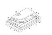
図1は一般的な交流形プラズマディスプレイパネルの一部斜視図である。 FIG. 1 is a partial perspective view of a general AC plasma display panel.
図1に示したように、プラズマディスプレイパネルは互いに対向して離れている二つのガラス基板1、6を含む。ガラス基板1上には走査電極4と維持電極5が対をなして平行に形成されており、走査電極4と維持電極5は誘電体層2及び保護膜3で覆われている。 ガラス基板6上には複数のアドレス電極8が形成されており、アドレス電極8は絶縁体層7で覆われている。アドレス電極8の間にある絶縁体層7上にはアドレス電極8と隔壁9が形成されている。また、絶縁体層7の表面及び隔壁9の両側面に蛍光体10が形成されている。ガラス基板1、6は走査電極4とアドレス電極8及び維持電極5とアドレス電極8が直交するように放電空間11を間に置いて対向して配置されている。アドレス電極8と、対をなす走査電極4と維持電極5との交差部にある放電空間11が放電セル12を形成する。
As shown in FIG. 1, the plasma display panel includes two
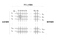
図2はプラズマ表示パネルの電極配列図を示す。 FIG. 2 shows an electrode array diagram of the plasma display panel.
図2に示したように、プラズマ表示パネルの電極はn×mのマトリックス形態を有しており、具体的に列方向にはアドレス電極A1〜Amが伸びていて、行方向には走査電極Y1〜Yn及び維持電極X1〜Xnが伸びている。図2に示された放電セル12は図1に示された放電セル12に対応する。
As shown in FIG. 2, the electrodes of the plasma display panel have an n × m matrix form. Specifically, the address electrodes A 1 to A m extend in the column direction and scan in the row direction. The electrodes Y 1 to Y n and the sustain electrodes X 1 to X n extend. The
一般にこのような交流形プラズマディスプレイパネルは1フレームが複数のサブフィールドに分けられて駆動され、サブフィールドの組み合わせによって階調が表現される。 In general, such an AC plasma display panel is driven with one frame divided into a plurality of subfields, and gradation is expressed by a combination of subfields.
そして交流形プラズマディスプレイパネルの駆動方法を時間的な動作変化で表現すれば、各サブフィールドはリセット期間、アドレス期間、維持期間からなる。 If the driving method of the AC type plasma display panel is expressed by temporal operation change, each subfield includes a reset period, an address period, and a sustain period.
リセット期間は直前の維持放電で形成された壁電荷を消去し、次のアドレス放電を安定的に行うために壁電荷を初期化する期間であり、アドレス期間はパネルで点灯されるセルと点灯されないセルを選択して点灯されるセル(アドレシングされたセル)に壁電荷を積む動作を行う期間である。そして維持期間はアドレシングされたセルに実際に画像を表示するための維持放電を行う期間である。 The reset period is a period for erasing the wall charge formed by the last sustain discharge and initializing the wall charge in order to stably perform the next address discharge. The address period is not lit with the cells lit on the panel. This is a period in which the operation of accumulating wall charges on a cell (addressed cell) that is lit by selecting a cell is performed. The sustain period is a period during which a sustain discharge is performed for actually displaying an image in the addressed cell.
一方、リセット期間は初期化対象となるセルに対して放電が発生するように各電極間に十分に高い電圧を印加するが、全セルの壁電荷状態を均一に制御するために弱放電が発生するように電圧を印加する。そしてリセット期間はアドレス期間がなければ維持期間で放電が発生しないように壁電荷を制御する。 On the other hand, during the reset period, a sufficiently high voltage is applied between the electrodes so that discharge is generated for the cell to be initialized, but weak discharge is generated to uniformly control the wall charge state of all cells. Apply a voltage to In the reset period, if there is no address period, the wall charges are controlled so that no discharge occurs in the sustain period.
しかし、パネル内電極に電圧を印加しないオフ状態から電源をオンする場合または電源をオフしてセル内の壁電荷状態がよく定義されていない状態で再び電源をオンする場合は、パネルの初期起動(パワーオン)時に数秒程度は低レベル放電をすることがある。 However, when the power is turned on from an off state where no voltage is applied to the electrode in the panel, or when the power is turned off and the power is turned on again when the wall charge state in the cell is not well defined, the initial startup of the panel At the time of (power on), low level discharge may occur for about several seconds.
また、明暗比や回路費用節減などの理由でリセット期間に印加する電圧の大きさを小さくした場合、初期起動時に瞬間的に低レベル放電をすることもある。 Also, when the magnitude of the voltage applied during the reset period is reduced for reasons such as light-to-dark ratio and circuit cost saving, a low level discharge may occur instantaneously at the initial startup.
プラズマディスプレイパネルにおける低レベル放電は、放電が正常に維持されないことを意味する。このような低レベル放電はセル内のプライミング粒子の不足やリセット期間によって制御できない壁電荷構造などによって、アドレス期間でのアドレス放電がよく行われないために発生する。 A low level discharge in the plasma display panel means that the discharge is not maintained normally. Such a low level discharge occurs because the address discharge is not often performed in the address period due to the shortage of priming particles in the cell or the wall charge structure that cannot be controlled by the reset period.
アドレス放電は、スキャンパルスとアドレスパルスが同時に印加される2〜3μs内外の短い電圧印加の瞬間に放電が形成されなければならない。しかし、セル内にプライミング粒子が不足する場合には放電が容易に形成されない。このような理由で長時間オフ状態を維持したパネルの初期起動時に、長い場合には数秒間も継続する低レベル放電をする確率が高い。そして電源オフ時に壁電荷状態が予測不可能になった後、直ちに再起動しても、パネルオフ時に形成された壁電荷状態を、リセット期間に初期化することができないため低レベル放電が発生する。 In the address discharge, a discharge must be formed at the moment of applying a short voltage within 2 to 3 μs when the scan pulse and the address pulse are applied simultaneously. However, when the priming particles are insufficient in the cell, the discharge is not easily formed. For this reason, at the initial startup of the panel that has been kept off for a long time, there is a high probability of low level discharge that lasts for several seconds if it is long. Even after restarting immediately after the wall charge state becomes unpredictable when the power is turned off, the wall charge state formed when the panel is turned off cannot be initialized in the reset period, resulting in low level discharge. .
このような低レベル放電を除去するために、従来は、非常に高い電圧を交互に印加する初期起動波形を使用した。しかし、このような初期起動波形により初期放電を行う場合、過度に強い放電が発生して回路にストレスを与えたり、そのための電源及び回路を備える費用が上昇する問題点がある。 In order to eliminate such a low level discharge, an initial startup waveform in which a very high voltage is alternately applied has been conventionally used. However, when initial discharge is performed using such an initial startup waveform, there is a problem in that excessively strong discharge occurs and stresses the circuit, and the cost of providing a power supply and a circuit therefor increases.
本発明が目的とする技術的課題はこのような従来の問題点を解決するためのものであって、プラズマディスプレイパネルの初期起動時に低レベル放電を除去できる初期起動方法を提供することである。 The technical problem aimed at by the present invention is to solve such a conventional problem, and is to provide an initial start-up method capable of removing a low level discharge at the initial start-up of a plasma display panel.
このような課題を解決するために本発明の一つの特徴によると、第1電極、第2電極によって放電セルが形成されるプラズマディスプレイパネルの電源がオンする時に操作される初期起動方法が提供される。この駆動方法はa)前記第1電極の電圧を第1電圧から第2電圧まで上昇させ、前記第2電極に第3電圧が印加される間に前記第1電極の電圧を第4電圧から第5電圧まで下降させて前記放電セルに壁電荷を形成する段階;及びb)前記放電セルの第1電極と第2電極との間の電圧差が交互に第6電圧または前記第6電圧の値で極性が負の電圧になるように前記第1電極と前記第2電極に電圧を印加して前記放電セルを放電させる段階を含む。 In order to solve such a problem, according to one aspect of the present invention, there is provided an initial startup method operated when a power source of a plasma display panel in which a discharge cell is formed by a first electrode and a second electrode is turned on. The In this driving method, a) the voltage of the first electrode is increased from the first voltage to the second voltage, and the voltage of the first electrode is changed from the fourth voltage to the second voltage while the third voltage is applied to the second electrode. Dropping to 5 voltage to form wall charges in the discharge cell; and b) the voltage difference between the first electrode and the second electrode of the discharge cell is alternately the sixth voltage or the value of the sixth voltage. And applying a voltage to the first electrode and the second electrode so that the polarity is a negative voltage, thereby discharging the discharge cell.
そして、入力される画像信号によってプラズマディスプレイパネルを駆動する場合に、サブフィールドはリセット期間、アドレス期間及び維持期間を含み、前記リセット期間は、前記第2電極に第7電圧を印加し、前記第1電極の電圧を第8電圧から第9電圧まで下降させる段階を含み、前記第3電圧と前記第5電圧の差は前記第7電圧と前記第9電圧の差より大きくする。この時、前記第3電圧は前記第7電圧より大きくすることができ、前記第5電圧は前記第9電圧より小さくすることもできる。そして前記第3電圧は、前記第1電極と第2電極との間の電圧差を前記第6電圧にするために前記第2電極に印加される電圧と同一にするすることもできる。 When the plasma display panel is driven by the input image signal, the subfield includes a reset period, an address period, and a sustain period. The reset period applies a seventh voltage to the second electrode, and A step of lowering the voltage of one electrode from the eighth voltage to the ninth voltage, wherein a difference between the third voltage and the fifth voltage is larger than a difference between the seventh voltage and the ninth voltage; At this time, the third voltage may be higher than the seventh voltage, and the fifth voltage may be lower than the ninth voltage. The third voltage may be the same as the voltage applied to the second electrode in order to make the voltage difference between the first electrode and the second electrode the sixth voltage.
そして本発明の他の特徴によると、第1電極、第2電極の間に放電セルが形成されるプラズマディスプレイパネル、そしてリセット期間、アドレス期間及び維持期間の間に前記第1電極及び第2電極に駆動電圧を印加する駆動回路を含み、前記駆動回路は前記プラズマディスプレイパネルの電源をオンにする時、前記第2電極に第1電圧を印加し、前記第1電極の電圧を第2電圧から第3電圧まで下降させた後、前記第1電極と前記第2電極に交互に第4電圧を印加する。この時、前記第4電圧は、前記維持期間で前記第1電極に印加される維持放電電圧と同一であり得る。 According to another aspect of the present invention, the plasma display panel in which a discharge cell is formed between the first electrode and the second electrode, and the first electrode and the second electrode during the reset period, the address period, and the sustain period. A driving circuit for applying a driving voltage to the plasma display panel, the driving circuit applies a first voltage to the second electrode when the plasma display panel is turned on, and the voltage of the first electrode is changed from the second voltage. After the voltage is lowered to the third voltage, a fourth voltage is alternately applied to the first electrode and the second electrode. At this time, the fourth voltage may be the same as the sustain discharge voltage applied to the first electrode in the sustain period.
本発明によれば、リセット期間で急激な電圧変動を防止して電流ピーク、素子ストレス、EMI及びノイズを減少させて回路動作の安定性及び信頼性を向上させることができる。 According to the present invention, it is possible to improve the stability and reliability of circuit operation by preventing sudden voltage fluctuations during the reset period and reducing current peaks, element stress, EMI, and noise.
以下、添付した図面を参照して本発明の実施例について本発明の属する技術分野における通常の知識を有する者が容易に実施することができるように詳細に説明する。しかし、本発明は多様で相異なる形態で実現することができ、ここで説明する実施例に限定されない。図面で本発明を明確に説明するために説明と関係ない部分は省略した。明細書全体にわたって類似な部分については同一な図面符号を付けた。 Hereinafter, embodiments of the present invention will be described in detail with reference to the accompanying drawings so that those skilled in the art to which the present invention pertains can easily implement the embodiments. However, the present invention can be implemented in various and different forms and is not limited to the embodiments described herein. In order to clearly describe the present invention in the drawings, portions not related to the description are omitted. Throughout the specification, similar parts are denoted by the same reference numerals.
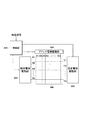
図3は本発明の実施例によるプラズマディスプレイパネルを示す図面である。 FIG. 3 illustrates a plasma display panel according to an embodiment of the present invention.
図3に示したように、本発明の実施例によるプラズマディスプレイパネルはプラズマパネル100、制御部200、アドレス電極駆動部300、維持電極駆動部400及び走査電極駆動部500を含む。
As shown in FIG. 3, the plasma display panel according to the embodiment of the present invention includes a
プラズマパネル100は列方向に長く配列されている複数のアドレス電極A1〜Am、行方向に長く配列されている複数の維持電極X1〜Xn及び走査電極Y1〜Ynを含む。
The
制御部200は外部から映像信号を受信してアドレス駆動制御信号、維持電極X駆動制御信号及び走査電極Y駆動制御信号を出力する。
The
アドレス電極駆動部300は制御部200からアドレス駆動制御信号を受信して表示しようとする放電セルを選択するための表示データ信号を各アドレス電極に印加する。
The
維持電極駆動部400は制御部200から維持電極X駆動制御信号を受信して維持電極Xに駆動電圧を印加する。
The
走査電極駆動部500は制御部200から走査電極Y駆動制御信号を受信して走査電極Yに駆動電圧を印加する。
The
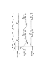
図4は本発明の第1実施例によるプラズマディスプレイパネルの駆動波形図である。 FIG. 4 is a driving waveform diagram of the plasma display panel according to the first embodiment of the present invention.
図4に示したようなプラズマディスプレイパネルの駆動波形は、一般的に、一つのフレーム期間を複数のサブフィールド期間に分け、更に、各サブフィールドをリセット期間Pr、アドレス期間Pa及び維持期間Psに分ける。そしてリセット期間は、上昇ランプ期間Pr1及び下降ランプ期間Pr2に分けられる。 Driving waveforms of the plasma display panel shown in FIG. 4, generally, one frame is divided into a period into a plurality of subfield periods, further each sub-field reset period P r, the address period P a and the sustain period divided into P s. The reset period is divided into a rising ramp period P r1 and a falling ramp period P r2 .
リセット期間Prの上昇ランプ期間Pr1は走査電極Y、維持電極X及びアドレス電極Aに壁電荷を形成する期間であり、下降ランプ期間Pr2は上昇ランプ期間Pr2で形成された壁電荷を一部消去してアドレス放電を容易にする期間である。そしてアドレス期間Paは複数の放電セルの中で維持期間で維持放電を起こす放電セルを選択する期間であり、維持期間Psは走査電極Yと維持電極Xに順次に維持パルスを印加してアドレス期間Paより選択された放電セルを維持放電させる期間である。 The rising ramp period P r1 of the reset period P r is a period in which wall charges are formed in the scan electrode Y, the sustain electrode X, and the address electrode A, and the falling ramp period P r2 is the wall charge formed in the rising ramp period P r2. This is a period during which part of the data is erased to facilitate address discharge. And the address period P a a period for selecting discharge cells causing sustain discharge in the sustain period among the plurality of discharge cells, the sustain period P s by applying sequentially sustain pulse to the sustain electrode X and the scan electrodes Y it is a period for maintaining discharge of the discharge cells selected by the address period P a.
そしてプラズマディスプレイパネルには各期間Pr、Pa、Psで走査電極Y及び維持電極Xに駆動電圧を印加する走査/維持駆動回路、そしてアドレス電極Aに駆動電圧を印加するアドレス駆動回路が連結されて一つの表示装置を構成する。 The plasma display panel includes a scan / sustain drive circuit that applies a drive voltage to the scan electrode Y and the sustain electrode X in each period P r , P a , and P s , and an address drive circuit that applies a drive voltage to the address electrode A. They are connected to form one display device.
図4に示すように、リセット期間Prの上昇ランプ期間Pr1ではアドレス電極A及び維持電極Xを零ボルトに維持し、走査電極YにVs電圧からVset電圧までなだらかに上昇するランプ電圧を印加する。このランプ電圧が上昇する間に全ての放電セルでは走査電極Yからアドレス電極A及び維持電極Xに各々微弱なリセット放電が起こる。その結果、走査電極Yの絶縁層上に(−)壁電荷が形成され、同時にアドレス電極A及び維持電極Xの絶縁層上には(+)壁電荷が形成される。 As shown in FIG. 4, in the rising ramp period P r1 of the reset period P r , the address electrode A and the sustain electrode X are maintained at zero volts, and the ramp voltage that gradually rises from the V s voltage to the V set voltage at the scan electrode Y. Apply. While the ramp voltage rises, weak reset discharge occurs from the scan electrode Y to the address electrode A and the sustain electrode X in all the discharge cells. As a result, a (−) wall charge is formed on the insulating layer of the scan electrode Y, and a (+) wall charge is simultaneously formed on the insulating layer of the address electrode A and the sustain electrode X.
ここで、壁電荷とは各電極を覆う絶縁性の壁(例えば、誘電体層)に形成されて蓄積される電荷のことを言う。このような壁電荷は、実際に電極自体に蓄積されることはないが、以下では、壁電荷が電極に“形成される”、“蓄積される”または“積まれる”のように説明される。また、壁電圧とは壁電荷によって、放電セルの電極と壁表面との間に形成される電位差のことを言う。 Here, the wall charge refers to a charge formed and accumulated on an insulating wall (for example, a dielectric layer) covering each electrode. Such wall charges are not actually stored on the electrode itself, but will be described below as wall charges are “formed”, “stored” or “stacked” on the electrode. . The wall voltage refers to a potential difference formed between the electrode of the discharge cell and the wall surface by wall charge.
リセット期間Prの下降ランプ期間Pr2では、維持電極Xを正の一定電圧Veに維持した状態で、走査電極Yには、正のVs電圧から負のVsc電圧に向かってなだらかに下降するランプ電圧を印加する。そして放電セルにおける放電開示電圧をVf電圧とした時、このランプ電圧が下降する間に走査電極Xとアドレス電極Yに各々負の電荷と正の電荷が積まれていて、一定量の壁電圧が形成されていれば、全ての放電セルにおいて、走査電極Yに印加される電圧がなだらかに正から負に向かって変化する間に、走査電極Y及び維持電極Xに印加された電圧と壁電圧との差が放電開示電圧Vfを超える場合に再び全ての放電セルでは微弱なリセット放電が発生して壁電荷が消去される。一般にVe−Vsc電圧を維持電極Xと走査電極Yとの間の放電開示電圧まで印加して維持電極Xと走査電極Yとの間の壁電圧をほとんど零ボルトに設定する。 In falling ramp period P r2 of the reset period P r, while maintaining the sustain electrode X to a constant positive voltage V e, the scan electrodes Y, gently towards the positive V s voltage to the negative V sc voltage Apply ramp-down voltage. When the discharge disclosure voltage in the discharge cell is Vf voltage, negative charges and positive charges are accumulated on the scan electrode X and the address electrode Y while the ramp voltage drops, and a certain amount of wall voltage is applied. Is formed, the voltage applied to the scan electrode Y and the sustain electrode X and the wall voltage while the voltage applied to the scan electrode Y gradually changes from positive to negative in all the discharge cells. If the difference between the two exceeds the discharge disclosure voltage Vf, a weak reset discharge occurs again in all the discharge cells, and the wall charges are erased. In general, the V e −V sc voltage is applied to the discharge disclosure voltage between the sustain electrode X and the scan electrode Y to set the wall voltage between the sustain electrode X and the scan electrode Y to almost zero volts.
そしてアドレス期間Paでは、維持電極Xと異なる走査電極Yを各々Ve電圧とVsch電圧に維持した状態で走査電極Yに順次にVsc電圧を印加して走査電極Yを選択する。そして負のVsc電圧が印加された走査電極Yによって形成される放電セルのうちの選択しようとする放電セルを形成するアドレス電極Aにアドレス電圧Vaを印加する。その結果、アドレス電極Aに印加された電圧Vaと走査電極Yに印加された電圧Vscの差及びアドレス電極A及び走査電極Yに形成された壁電荷による壁電圧によってアドレス電極Aと走査電極Yとの間及び維持電極Xと走査電極Yとの間でアドレス放電が起こる。その結果、走査電極Yには(+)壁電荷が形成され、維持電極Xには(−)壁電荷が形成される。 Then, in the address period P a, by applying a respective V e voltage and V sch sequentially V sc voltage while maintaining a voltage to the scan electrodes Y a scan electrode Y different from the sustain electrode X to select the scan electrodes Y. The negative V sc voltage is applied to the address electrode A in the address voltage V a to form a discharge cell to be selected from among the discharge cells formed by the applied scan electrodes Y. As a result, the scanning and address electrodes A by the difference and the address electrode A and the wall voltage due to wall charges formed on the scan electrodes Y of the applied voltage V sc and voltage V a applied to the address electrode A to the scan electrodes Y electrodes Address discharge occurs between Y and the sustain electrode X and the scan electrode Y. As a result, (+) wall charges are formed on the scan electrode Y, and (−) wall charges are formed on the sustain electrode X.
次に、維持期間Psでは走査電極Yと維持電極Xに順次に維持パルスが印加される。維持パルスは走査電極Yと維持電極Xの電圧差が交互にVs電圧及び−Vs電圧になるようにするパルスである。Vs電圧は走査電極Yと維持電極Xとの間の放電開示電圧より低い電圧である。アドレス期間Paでアドレス放電によって走査電極Yと維持電極Xとの間に壁電圧が形成されていれば、壁電圧とVs電圧によって走査電極Yと維持電極Xで放電が起こる。 Then, sequentially sustain pulse to the sustain electrodes X and the sustain period P s the scan electrode Y is applied. Sustain pulse is a pulse to make the voltage difference between the sustain electrode X and the scan electrode Y becomes V s voltage and -V s voltage alternately. V s the voltage is a voltage lower than the discharge initiation voltage between the sustain electrode X and the scan electrode Y. If the wall voltage is formed between the address discharge and the scan electrodes Y and the sustain electrode X in the address period P a, discharge scanning electrodes Y and the sustain electrode X by the wall voltage and V s voltage occurs.
一方、図4では一つのフレームを形成する複数のサブフィールドのうちの第1サブフィールドには主リセット期間Pr_mainが形成されており、その後のサブフィールドには副リセット期間Pr_subが形成されている。 On the other hand, it is formed the main reset period P R_main the first subfield among the plurality of subfields forming one frame in FIG. 4, and subsequent to the subfield sub reset period P R_sub formed Yes.
第1サブフィールドのリセット期間である主リセット期間Pr_mainでは上昇ランプ波形が印加された後、下降ランプ波形が印加される。そして2番目以後のサブフィールドリセット期間である副リセット期間Pr_subでは下降ランプ波形のみが印加される。 In the main reset period Pr_main which is the reset period of the first subfield, the rising ramp waveform is applied and then the falling ramp waveform is applied. In the sub-reset period P r_sub which is the second and subsequent sub-field reset periods, only the falling ramp waveform is applied.
一般にリセット期間で放電セルに多量の壁電荷を形成するために前述のように走査電極Yに上昇ランプ波形を印加する。しかし、2番目以降のサブフィールドでは直前サブフィールドの維持期間で発光した放電セルには維持放電によって既に多量の壁電荷が形成されているので、リセット期間で壁電荷を形成する必要がない。また、維持期間で発光しない放電セルにはリセット期間で形成された壁電荷状態が変更されなかったために、次のサブフィールドでは再びリセット動作を行わなくてもよい。そしてこの状態で走査電極Yに下降ランプ波形のみ印加すれば放電が起こらないので放電セルはリセットされた状態を維持する。そして図4では1フレームを基準にして第1サブフィールドにのみ主リセット期間Pr_mainを置いたが、これとは異なって他のサブフィールドにも主リセット期間Pr_mainを置くことができる。 In general, a rising ramp waveform is applied to the scan electrode Y as described above in order to form a large amount of wall charges in the discharge cell during the reset period. However, in the second and subsequent subfields, since a large amount of wall charges have already been formed by the sustain discharge in the discharge cells that have emitted light in the sustain period of the immediately preceding subfield, it is not necessary to form wall charges in the reset period. Further, since the wall charge state formed in the reset period is not changed in the discharge cells that do not emit light in the sustain period, the reset operation may not be performed again in the next subfield. In this state, if only the falling ramp waveform is applied to the scan electrode Y, no discharge occurs, so that the discharge cell maintains the reset state. And although placed main reset period P R_main only 4 one frame in the first sub-field as a reference, this to be able to put the main reset period P R_main to other subfields differently.
本発明の実施例では図4のような駆動波形になるように駆動させるためにプラズマディスプレイパネルのパワーをオンする時に発生する可能性がある低レベル放電を除去できる初期起動波形を挿入する。 In the embodiment of the present invention, in order to drive the driving waveform as shown in FIG. 4, an initial startup waveform that can remove a low level discharge that may occur when the power of the plasma display panel is turned on is inserted.
以下、図5を参照して本発明の実施例によるプラズマディスプレイパネルの初期起動波形について詳細に説明する。 Hereinafter, an initial startup waveform of the plasma display panel according to the embodiment of the present invention will be described in detail with reference to FIG.
図5は本発明の実施例によるプラズマディスプレイパネルの初期起動波形を示した図面である。 FIG. 5 is a diagram illustrating initial startup waveforms of a plasma display panel according to an embodiment of the present invention.
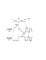
図5に示したように、本発明の実施例によるプラズマディスプレイパネルの初期起動波形は全セル壁電荷形成期間Prr及び全セル放電期間Pssを含む。 As shown in FIG. 5, the initial start-up waveforms of the plasma display panel according to an embodiment of the present invention comprises whole cell wall charge forming period P rr and total cell discharge period P ss.
全セル壁電荷形成期間Prrは維持期間で維持放電を起こす放全セルを選択するアドレス期間がなくても全セル放電期間Pssで維持パルス印加によって全セルに放電が発生できるように壁電荷を形成する期間であり、全セル放電期間Pssは走査電極Yと維持電極Xに順次に維持パルスを印加して全セルを放電させる期間である。 The wall charge formation period Prr is a wall charge so that a discharge can be generated in all the cells by applying a sustain pulse in the all-cell discharge period Pss even if there is no address period for selecting a release cell that causes a sustain discharge in the sustain period. The all-cell discharge period Pss is a period in which the sustain pulses are sequentially applied to the scan electrodes Y and the sustain electrodes X to discharge all the cells.
全セル壁電荷形成期間Prrは電圧上昇期間及び電圧下降期間を含む。 The all cell wall charge formation period Prr includes a voltage increase period and a voltage decrease period.
全セル壁電荷形成期間Prrの電圧上昇期間Prr1は図4のリセット期間Prの上昇ランプ期間Pr1におけるようにアドレス電極A及び維持電極Xを零ボルトに維持し、走査電極YにVs電圧からVset電圧までなだらかに上昇するランプ電圧を印加する。このランプ電圧が上昇する間に全ての放全セルでは走査電極Yからアドレス電極A及び維持電極Xに各々微弱なリセット放電が起こる。その結果、走査電極Yに(−)壁電荷が形成され、同時に維持電極Xには(+)壁電荷が形成される。 The voltage rising period P rr1 of the all cell wall charge forming period P rr maintains the address electrode A and the sustain electrode X at zero volts as in the rising ramp period P r1 of the reset period P r in FIG. A ramp voltage that rises gently from the s voltage to the V set voltage is applied. While this ramp voltage rises, weak reset discharge occurs from the scan electrode Y to the address electrode A and the sustain electrode X in all discharge cells. As a result, (−) wall charges are formed on the scan electrodes Y, and (+) wall charges are formed on the sustain electrodes X at the same time.
そして全セル壁電荷形成期間Prrの電圧下降期間Prr2は維持電極Xを一定電圧であるVeより高い電圧Vbに維持した状態で、走査電極YにVs電圧からVsc電圧に向かってなだらかに下降するランプ電圧を印加する。 And while the voltage falling period P rr2 of all the cells the wall charge forming period P rr is maintaining the sustain electrode X at a high voltage V b from V e is a constant voltage, toward the V s voltage V sc voltage to the scan electrodes Y Apply a ramp voltage that falls gently.
[数式1]
│Vb−Vsc│>│Ve−Vsc│
つまり、全セル壁電荷形成期間Prrの電圧下降期間Prr2では数式1のように走査電極Yと維持電極Xとの間の最終印加電圧の大きさが図4の下降ランプ期間での走査電極Yと維持電極Xとの間の最終印加電圧の大きさより大きい。一般に走査電極に印加される電圧がなだらかに減少する途中に全セル壁電荷形成期間Prrにおいて形成された壁電圧と走査電極Yと維持電極Xに印加された電圧差が放電開示電圧を超える場合には放電が起こり、走査電極Yと維持電極Xに印加された電圧差が維持電極Xと走査電極Yとの間で放電を起こすことがある放電開示電圧−Vfまで減少すれば維持電極Xと走査電極Yとの間の壁電圧はほとんど零ボルトとなる。
[Formula 1]
│V b -V sc │> │V e -V sc │
That is, in the voltage drop period P rr2 of the all cell wall charge formation period P rr , the magnitude of the final applied voltage between the scan electrode Y and the sustain electrode X is equal to the scan electrode in the drop ramp period of FIG. It is larger than the magnitude of the final applied voltage between Y and the sustain electrode X. In general, the difference between the wall voltage formed in the all-cell wall charge formation period Prr and the voltage applied to the scan electrode Y and the sustain electrode X exceeds the discharge disclosure voltage while the voltage applied to the scan electrode is gradually decreasing. If a discharge occurs, and the voltage difference applied to scan electrode Y and sustain electrode X decreases to discharge disclosed voltage −V f that may cause a discharge between sustain electrode X and scan electrode Y, sustain electrode X And the scan electrode Y are almost zero volts.
次に、走査電極Yと維持電極Xに印加された電圧差が−Vf電圧以下になれば、走査電極Yは(+)壁電荷が形成され、同時にアドレス電極A及び維持電極Xには(−)壁電荷が形成されて壁電圧が高くなる。結局、前述した図4の駆動波形を有するアドレス期間でのアドレス放電と同一な役割を果たす。この時、Vbは|Vb−Vsc|の大きさが全セル壁電荷形成期間以後に維持パルスを印加しても放電が起こる程度の大きさとする。 Then, if the voltage difference is applied to the scan electrodes Y and the sustain electrode X becomes equal to or less than -V f voltage, the scan electrode Y (+) wall charges are formed on the address electrode A and the sustain electrode X at the same time ( -) Wall charges are formed and the wall voltage increases. After all, it plays the same role as the address discharge in the address period having the driving waveform of FIG. At this time, V b is set such that | V b −V sc | is such that discharge occurs even if a sustain pulse is applied after the all-cell wall charge formation period.
そして全セル放電期間Pssでは図4の駆動波形でのように走査電極Yと維持電極Xに順次に維持パルスが印加される。この時、全ての放電セルは全セル壁電荷形成期間Prrで蓄積された壁電荷による壁電圧と維持パルスによるVs電圧によって走査電極Yと維持電極Xで放電が起こる。この放電過程で全てのセル内に十分な放電プライミングが供給され、同時に全セルの壁電荷状態が制御可能な領域に存在するようになって初期低レベル放電現象が除去できる。 In the all-cell discharge period P ss , the sustain pulse is sequentially applied to the scan electrode Y and the sustain electrode X as in the drive waveform of FIG. At this time, all the discharge cells discharge occurs scan electrodes Y and the sustain electrode X by V s voltage due to the wall voltage and sustain pulses by the wall charges accumulated in all cell wall charge forming period P rr. In this discharge process, sufficient discharge priming is supplied to all the cells, and at the same time, the wall charge state of all the cells exists in a controllable region, so that the initial low level discharge phenomenon can be removed.
そして本発明の第1実施例では電圧下降期間Prr2の最終印加電圧|Vb−Vsc|の大きさを放電開示電圧より大きくするために維持電極XにVe電圧より高いVb電圧を印加したが、これはVb電圧を供給する別途の電源が追加されなければならない。したがって、Vb電圧の代りにVs電圧を印加することもできる。このようにすれば、別途の電源を追加する必要はない。 The final applied voltage of the voltage falling period P rr2 in the first embodiment of the present invention | was applied higher than V e voltage on the sustain electrode X to be greater than the discharge initiation voltage magnitude Vb voltage | V b -Vsc However, this requires an additional power supply to supply the Vb voltage. Therefore, it is also possible to apply a V s voltage instead of the V b voltage. In this way, it is not necessary to add a separate power source.
そして本発明の第1実施例では維持電極Xに印加された電圧下降期間Prr2の電圧を変更して低レベル放電を除去したが、これと異なるようにすることもできる。このような実施例について図6を参照して詳細に説明する。 In the first embodiment of the present invention, the low level discharge is removed by changing the voltage of the voltage falling period Prr2 applied to the sustain electrode X, but it may be different from this. Such an embodiment will be described in detail with reference to FIG.
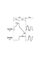
図6は本発明の第2実施例によるプラズマディスプレイパネルの初期起動波形を示した図面である。 FIG. 6 is a diagram illustrating an initial startup waveform of the plasma display panel according to the second embodiment of the present invention.
図6に示すように、本発明の第2実施例によるプラズマディスプレイパネルの初期起動波形で全セル壁電荷形成期間Prrの電圧下降期間Prr2では図5の電圧下降期間Prr2に印加されたVsc電圧よりさらに低いVnf電圧に向かってなだらかに下降するランプ電圧を印加する。
[数式2]
│Vb−Vnf│>│Vb−Vsc│>│Ve−Vsc│
つまり、電圧下降期間Prr2では数式2のように走査電極Yと維持電極Xの間の最終印加電圧の大きさが図5の電圧下降期間Prr2におけるより大きい。このようにすれば、図5におけるより更に多くの壁電荷が形成される。つまり、走査電極Yと維持電極Xに蓄積された壁電荷の消去される量が図5の駆動波形におけるより減少して直ちに維持パルスを印加しても放電が起こるようになる。
As shown in FIG. 6, it is applied to the voltage falling period P rr2 second initial start waveform in all cell wall charge forming period of the plasma display panel according to Example P rr voltage falling period P rr2 In Figure 5 of the present invention A ramp voltage that gradually falls toward a V nf voltage lower than the V sc voltage is applied.
[Formula 2]
│V b -V nf │> │V b -V sc │> │V e -V sc │
That is, in the voltage drop period P rr2 , the magnitude of the final applied voltage between the scan electrode Y and the sustain electrode X is larger in the voltage drop period P rr2 in FIG. In this way, more wall charges are formed than in FIG. That is, the amount of wall charges accumulated in the scan electrode Y and the sustain electrode X is erased more than in the drive waveform of FIG.
そして本発明の第2実施例とは異なって、維持電極XにVe電圧を印加し、走査電極YにVnf電圧を印加することもできる。 And unlike the second embodiment of the present invention may be a V e voltage is applied to the sustain electrodes X, and applies the V nf voltage to the scan electrodes Y.
そして本発明の実施例によるプラズマディスプレイパネルの初期起動波形はパネルの電源オン時にのみ印加されるので、多様なシークエンスで構成することができる。全セル壁電荷形成期間を1回以上繰り返した後、全セル放電期間を数回以上繰り返すことができる。 そしてこれとは異なって全セル壁電荷形成期間後、全セル放電期間を数回以上繰り返し、全体を再び数回以上繰り返すこともできる。このようにすれば、初期起動動作のための電源や回路を別途に備えなくても放電開示電圧より小さい維持パルスの交互印加によって安定な初期起動動作を行うことができる。 Since the initial startup waveform of the plasma display panel according to the embodiment of the present invention is applied only when the panel is turned on, the plasma display panel can be configured with various sequences. After repeating the all-cell wall charge formation period once or more, the all-cell discharge period can be repeated several times or more. In contrast to this, the whole cell discharge period can be repeated several times or more after the all cell wall charge formation period, and the whole can be repeated again several times or more. In this way, it is possible to perform a stable initial startup operation by alternately applying a sustain pulse smaller than the discharge disclosure voltage without separately providing a power source and a circuit for the initial startup operation.
そして本発明の第1及び第2実施例では走査電極Yの電圧をランプ形態でなだらかに下降させたが、これとは異なって階段波形態で変更することもでき、パルス印加とフローティングの交替操作、または抵抗と静電容量による時定数設定を利用した時間によって変わる波形を印加することもできる。 In the first and second embodiments of the present invention, the voltage of the scan electrode Y is gently lowered in the form of a ramp. However, it can be changed in the form of a stepped wave, and the operation of switching between pulse application and floating is different. Alternatively, it is possible to apply a waveform that changes with time using a time constant setting based on resistance and capacitance.
以上、本発明の好ましい実施例について詳細に説明したが、本発明の権利範囲はこれに限定されず、請求範囲で定義している本発明の基本概念を利用した当業者の多様な変形及び改良形態もまた本発明の権利範囲に属する。 The preferred embodiments of the present invention have been described in detail above, but the scope of the present invention is not limited thereto, and various modifications and improvements of those skilled in the art using the basic concept of the present invention defined in the claims. Forms are also within the scope of the present invention.
100 プラズマパネル
200 制御部
300 アドレス電極駆動部
400 維持電極駆動部
500 走査電極駆動部
A1〜Am アドレス電極
X1〜Xn 維持電極
Y1〜Yn 走査電極
Pa アドレス期間
Pr リセット期間
Pr1 上昇ランプ期間
Pr2 下降ランプ期間
Prr 全セル壁電荷形成期間
Prr2 電圧下降期間
Pr_main 主リセット期間
Pr_sub 副リセット期間
Ps 維持期間
Pss 全セル放電期間
Va アドレス電極に印加された電圧
Vsc 走査電極に印加された電圧
100
Claims (9)
a)前記第1電極の電圧を第1電圧から第2電圧まで上昇させ、前記第2電極に第3電圧が印加される間に前記第1電極の電圧を第4電圧から第5電圧まで下降させて前記放電セルに壁電荷を形成する段階、
b)前記放電セルに壁電荷が形成された直後に、前記放電セルの第1電極と第2電極との間の電圧差が、交互に第6電圧または前記第6電圧の値で極性が負の電圧になるように前記第1電極と前記第2電極に電圧を印加して前記放電セルを放電させる段階、
を含む、プラズマディスプレイパネルの初期起動方法。 In the initial startup method operated when the power of the plasma display panel in which the discharge cell is formed by the first electrode and the second electrode is turned on,
a) The voltage of the first electrode is increased from the first voltage to the second voltage, and the voltage of the first electrode is decreased from the fourth voltage to the fifth voltage while the third voltage is applied to the second electrode. Forming a wall charge in the discharge cell,
b) Immediately after the wall charge is formed in the discharge cell, the voltage difference between the first electrode and the second electrode of the discharge cell is alternately negative at the sixth voltage or the value of the sixth voltage. Applying a voltage to the first electrode and the second electrode such that the discharge cell is discharged,
An initial start-up method of a plasma display panel, including:
前記リセット期間は、前記第2電極に第7電圧を印加し、前記第1電極の電圧を第8電圧から第9電圧まで下降させる段階を含み、
前記第3電圧と前記第5電圧の差は、前記第7電圧と前記第9電圧の差より大きい、請求項1に記載のプラズマディスプレイパネルの初期起動方法。 When the plasma display panel is driven by an input image signal, the subfield includes a reset period, an address period, and a sustain period.
The reset period includes applying a seventh voltage to the second electrode and lowering the voltage of the first electrode from an eighth voltage to a ninth voltage,
The method of claim 1, wherein a difference between the third voltage and the fifth voltage is greater than a difference between the seventh voltage and the ninth voltage.
リセット期間、アドレス期間及び維持期間の間に前記第1電極及び第2電極に駆動電圧を印加する駆動回路を含み、
前記駆動回路は、前記プラズマディスプレイパネルの電源がオンする時、前記第2電極に第1電圧を印加した状態で、前記第1電極の電圧を第2電圧から第3電圧まで下降させて、前記第1電極の電圧が前記第3電圧まで下降され前記放電セルに壁電荷が形成された直後に、前記第1電極と前記第2電極に交互に第4電圧を印加して前記放電セルを維持放電させるプラズマ表示装置。 A plasma display panel in which a discharge cell is formed between the first electrode and the second electrode;
A driving circuit for applying a driving voltage to the first electrode and the second electrode during a reset period, an address period, and a sustain period;
The driving circuit lowers the voltage of the first electrode from the second voltage to the third voltage in a state where the first voltage is applied to the second electrode when the power of the plasma display panel is turned on . Immediately after the voltage of the first electrode is lowered to the third voltage and wall charges are formed in the discharge cell, a fourth voltage is applied alternately to the first electrode and the second electrode to Plasma display device for sustain discharge .
前記第1電圧と前記第3電圧の差は、前記第5電圧と前記第7電圧の差より大きい、請求項7に記載のプラズマ表示装置。 In the reset period, a fifth voltage is applied to the second electrode, and the voltage of the first electrode is decreased from a sixth voltage to a seventh voltage,
The plasma display device according to claim 7, wherein a difference between the first voltage and the third voltage is larger than a difference between the fifth voltage and the seventh voltage.
Applications Claiming Priority (1)
| Application Number | Priority Date | Filing Date | Title |
|---|---|---|---|
| KR1020040024869A KR100589349B1 (en) | 2004-04-12 | 2004-04-12 | Initial startup method of plasma display panel and plasma display device |
Publications (2)
| Publication Number | Publication Date |
|---|---|
| JP2005301278A JP2005301278A (en) | 2005-10-27 |
| JP4206397B2 true JP4206397B2 (en) | 2009-01-07 |
Family
ID=35060063
Family Applications (1)
| Application Number | Title | Priority Date | Filing Date |
|---|---|---|---|
| JP2005112268A Expired - Fee Related JP4206397B2 (en) | 2004-04-12 | 2005-04-08 | Initial startup method of plasma display panel and plasma display device |
Country Status (4)
| Country | Link |
|---|---|
| US (1) | US7825874B2 (en) |
| JP (1) | JP4206397B2 (en) |
| KR (1) | KR100589349B1 (en) |
| CN (1) | CN100474367C (en) |
Families Citing this family (6)
| Publication number | Priority date | Publication date | Assignee | Title |
|---|---|---|---|---|
| US7365710B2 (en) * | 2003-09-09 | 2008-04-29 | Samsung Sdi Co. Ltd. | Plasma display panel driving method and plasma display device |
| KR100680709B1 (en) * | 2004-12-23 | 2007-02-08 | 엘지전자 주식회사 | Driving device of plasma display panel |
| CN100362548C (en) * | 2006-01-11 | 2008-01-16 | 四川世纪双虹显示器件有限公司 | Method for driving plasma display panel in reset period and addressing period |
| US20080165175A1 (en) * | 2007-01-09 | 2008-07-10 | Yoo-Jin Song | Plasma display and driving method thereof |
| KR20080103419A (en) * | 2007-05-23 | 2008-11-27 | 삼성에스디아이 주식회사 | Plasma display |
| KR100970488B1 (en) * | 2008-07-24 | 2010-07-16 | 삼성에스디아이 주식회사 | Plasma display device and driving method thereof |
Family Cites Families (10)
| Publication number | Priority date | Publication date | Assignee | Title |
|---|---|---|---|---|
| JP3556097B2 (en) | 1998-06-30 | 2004-08-18 | 富士通株式会社 | Plasma display panel driving method |
| JP2002072957A (en) * | 2000-08-24 | 2002-03-12 | Matsushita Electric Ind Co Ltd | Driving method of plasma display panel |
| JP2002175043A (en) | 2000-12-06 | 2002-06-21 | Nec Corp | Method for driving plasma display panel, and circuit and display device thereof |
| KR100452688B1 (en) | 2001-10-10 | 2004-10-14 | 엘지전자 주식회사 | Driving method for plasma display panel |
| JP4138292B2 (en) | 2001-10-26 | 2008-08-27 | パイオニア株式会社 | Driving method of AC type plasma display |
| KR100493912B1 (en) | 2001-11-24 | 2005-06-10 | 엘지전자 주식회사 | Apparatus and method for driving of plasma display panel |
| US7012579B2 (en) * | 2001-12-07 | 2006-03-14 | Lg Electronics Inc. | Method of driving plasma display panel |
| KR100475161B1 (en) * | 2002-04-04 | 2005-03-08 | 엘지전자 주식회사 | Method for driving of plasma display panel |
| EP1387344A3 (en) * | 2002-08-01 | 2006-07-26 | Lg Electronics Inc. | Method and apparatus for driving plasma display panel |
| JP2004086076A (en) | 2002-08-29 | 2004-03-18 | Sony Corp | Display device, its driving circuit, and driving method |
-
2004
- 2004-04-12 KR KR1020040024869A patent/KR100589349B1/en not_active Expired - Fee Related
-
2005
- 2005-04-08 JP JP2005112268A patent/JP4206397B2/en not_active Expired - Fee Related
- 2005-04-11 US US11/104,229 patent/US7825874B2/en not_active Expired - Fee Related
- 2005-04-12 CN CNB2005100649535A patent/CN100474367C/en not_active Expired - Fee Related
Also Published As
| Publication number | Publication date |
|---|---|
| CN100474367C (en) | 2009-04-01 |
| JP2005301278A (en) | 2005-10-27 |
| KR20050099698A (en) | 2005-10-17 |
| KR100589349B1 (en) | 2006-06-14 |
| CN1684125A (en) | 2005-10-19 |
| US20050225508A1 (en) | 2005-10-13 |
| US7825874B2 (en) | 2010-11-02 |
Similar Documents
| Publication | Publication Date | Title |
|---|---|---|
| JP4109098B2 (en) | Driving method of plasma display panel | |
| CN100392710C (en) | Driving method of plasma display panel | |
| JP4339041B2 (en) | Plasma display panel and driving method thereof | |
| JP2002278510A (en) | Driving method and display device for plasma display panel | |
| JP4655090B2 (en) | Plasma display panel driving method and plasma display device | |
| US7564429B2 (en) | Plasma display apparatus and driving method thereof | |
| JP4530048B2 (en) | Plasma display apparatus and driving method of plasma display panel | |
| EP1717786A2 (en) | Plasma display apparatus and image processing method thereof | |
| JP4055740B2 (en) | Driving method of plasma display panel | |
| JP2005122102A (en) | Plasma display panel and driving method thereof | |
| US7446734B2 (en) | Method of driving plasma display panel | |
| JP4206397B2 (en) | Initial startup method of plasma display panel and plasma display device | |
| JP3988728B2 (en) | Driving method of plasma display panel | |
| KR100421672B1 (en) | Driving Method for scanning of Plasma Display Panel | |
| JP2006293113A (en) | Plasma display panel driving method and plasma display device | |
| JP4956911B2 (en) | Driving method of plasma display panel | |
| JP4813150B2 (en) | Plasma display device and driving method thereof | |
| JP4639579B2 (en) | Driving method of plasma display panel | |
| CN101578647B (en) | Plasma display panel display device and driving method therefor | |
| KR100590099B1 (en) | Driving Method of Plasma Display Panel and Plasma Display | |
| KR100560522B1 (en) | Driving Method of Plasma Display Panel and Plasma Display | |
| KR100560513B1 (en) | Driving Method of Plasma Display Panel and Plasma Display | |
| JP2007163736A (en) | Driving method of plasma display panel | |
| KR100599616B1 (en) | Driving Method of Plasma Display Panel and Plasma Display | |
| KR100578834B1 (en) | Plasma Display Panel and Driving Method thereof |
Legal Events
| Date | Code | Title | Description |
|---|---|---|---|
| A131 | Notification of reasons for refusal |
Free format text: JAPANESE INTERMEDIATE CODE: A131 Effective date: 20080603 |
|
| A601 | Written request for extension of time |
Free format text: JAPANESE INTERMEDIATE CODE: A601 Effective date: 20080903 |
|
| A602 | Written permission of extension of time |
Free format text: JAPANESE INTERMEDIATE CODE: A602 Effective date: 20080908 |
|
| A521 | Request for written amendment filed |
Free format text: JAPANESE INTERMEDIATE CODE: A523 Effective date: 20080909 |
|
| TRDD | Decision of grant or rejection written | ||
| A01 | Written decision to grant a patent or to grant a registration (utility model) |
Free format text: JAPANESE INTERMEDIATE CODE: A01 Effective date: 20081014 |
|
| A01 | Written decision to grant a patent or to grant a registration (utility model) |
Free format text: JAPANESE INTERMEDIATE CODE: A01 |
|
| A61 | First payment of annual fees (during grant procedure) |
Free format text: JAPANESE INTERMEDIATE CODE: A61 Effective date: 20081020 |
|
| FPAY | Renewal fee payment (event date is renewal date of database) |
Free format text: PAYMENT UNTIL: 20111024 Year of fee payment: 3 |
|
| R150 | Certificate of patent or registration of utility model |
Free format text: JAPANESE INTERMEDIATE CODE: R150 |
|
| FPAY | Renewal fee payment (event date is renewal date of database) |
Free format text: PAYMENT UNTIL: 20111024 Year of fee payment: 3 |
|
| FPAY | Renewal fee payment (event date is renewal date of database) |
Free format text: PAYMENT UNTIL: 20121024 Year of fee payment: 4 |
|
| FPAY | Renewal fee payment (event date is renewal date of database) |
Free format text: PAYMENT UNTIL: 20121024 Year of fee payment: 4 |
|
| FPAY | Renewal fee payment (event date is renewal date of database) |
Free format text: PAYMENT UNTIL: 20131024 Year of fee payment: 5 |
|
| R250 | Receipt of annual fees |
Free format text: JAPANESE INTERMEDIATE CODE: R250 |
|
| LAPS | Cancellation because of no payment of annual fees |