JP4199801B2 - 共振周波数タグ、および共振周波数タグの制御方法 - Google Patents
共振周波数タグ、および共振周波数タグの制御方法 Download PDFInfo
- Publication number
- JP4199801B2 JP4199801B2 JP2006508623A JP2006508623A JP4199801B2 JP 4199801 B2 JP4199801 B2 JP 4199801B2 JP 2006508623 A JP2006508623 A JP 2006508623A JP 2006508623 A JP2006508623 A JP 2006508623A JP 4199801 B2 JP4199801 B2 JP 4199801B2
- Authority
- JP
- Japan
- Prior art keywords
- conductor pattern
- land
- tag
- frequency
- conductor
- Prior art date
- Legal status (The legal status is an assumption and is not a legal conclusion. Google has not performed a legal analysis and makes no representation as to the accuracy of the status listed.)
- Expired - Fee Related
Links
Images


Classifications
-
- H—ELECTRICITY
- H01—ELECTRIC ELEMENTS
- H01F—MAGNETS; INDUCTANCES; TRANSFORMERS; SELECTION OF MATERIALS FOR THEIR MAGNETIC PROPERTIES
- H01F41/00—Apparatus or processes specially adapted for manufacturing or assembling magnets, inductances or transformers; Apparatus or processes specially adapted for manufacturing materials characterised by their magnetic properties
- H01F41/02—Apparatus or processes specially adapted for manufacturing or assembling magnets, inductances or transformers; Apparatus or processes specially adapted for manufacturing materials characterised by their magnetic properties for manufacturing cores, coils, or magnets
- H01F41/04—Apparatus or processes specially adapted for manufacturing or assembling magnets, inductances or transformers; Apparatus or processes specially adapted for manufacturing materials characterised by their magnetic properties for manufacturing cores, coils, or magnets for manufacturing coils
- H01F41/041—Printed circuit coils
-
- G—PHYSICS
- G06—COMPUTING; CALCULATING OR COUNTING
- G06K—GRAPHICAL DATA READING; PRESENTATION OF DATA; RECORD CARRIERS; HANDLING RECORD CARRIERS
- G06K19/00—Record carriers for use with machines and with at least a part designed to carry digital markings
- G06K19/06—Record carriers for use with machines and with at least a part designed to carry digital markings characterised by the kind of the digital marking, e.g. shape, nature, code
- G06K19/067—Record carriers with conductive marks, printed circuits or semiconductor circuit elements, e.g. credit or identity cards also with resonating or responding marks without active components
- G06K19/07—Record carriers with conductive marks, printed circuits or semiconductor circuit elements, e.g. credit or identity cards also with resonating or responding marks without active components with integrated circuit chips
- G06K19/077—Constructional details, e.g. mounting of circuits in the carrier
-
- G—PHYSICS
- G06—COMPUTING; CALCULATING OR COUNTING
- G06K—GRAPHICAL DATA READING; PRESENTATION OF DATA; RECORD CARRIERS; HANDLING RECORD CARRIERS
- G06K19/00—Record carriers for use with machines and with at least a part designed to carry digital markings
- G06K19/06—Record carriers for use with machines and with at least a part designed to carry digital markings characterised by the kind of the digital marking, e.g. shape, nature, code
- G06K19/067—Record carriers with conductive marks, printed circuits or semiconductor circuit elements, e.g. credit or identity cards also with resonating or responding marks without active components
- G06K19/07—Record carriers with conductive marks, printed circuits or semiconductor circuit elements, e.g. credit or identity cards also with resonating or responding marks without active components with integrated circuit chips
- G06K19/0723—Record carriers with conductive marks, printed circuits or semiconductor circuit elements, e.g. credit or identity cards also with resonating or responding marks without active components with integrated circuit chips the record carrier comprising an arrangement for non-contact communication, e.g. wireless communication circuits on transponder cards, non-contact smart cards or RFIDs
- G06K19/0726—Record carriers with conductive marks, printed circuits or semiconductor circuit elements, e.g. credit or identity cards also with resonating or responding marks without active components with integrated circuit chips the record carrier comprising an arrangement for non-contact communication, e.g. wireless communication circuits on transponder cards, non-contact smart cards or RFIDs the arrangement including a circuit for tuning the resonance frequency of an antenna on the record carrier
-
- G—PHYSICS
- G06—COMPUTING; CALCULATING OR COUNTING
- G06K—GRAPHICAL DATA READING; PRESENTATION OF DATA; RECORD CARRIERS; HANDLING RECORD CARRIERS
- G06K19/00—Record carriers for use with machines and with at least a part designed to carry digital markings
- G06K19/06—Record carriers for use with machines and with at least a part designed to carry digital markings characterised by the kind of the digital marking, e.g. shape, nature, code
- G06K19/067—Record carriers with conductive marks, printed circuits or semiconductor circuit elements, e.g. credit or identity cards also with resonating or responding marks without active components
- G06K19/07—Record carriers with conductive marks, printed circuits or semiconductor circuit elements, e.g. credit or identity cards also with resonating or responding marks without active components with integrated circuit chips
- G06K19/077—Constructional details, e.g. mounting of circuits in the carrier
- G06K19/07718—Constructional details, e.g. mounting of circuits in the carrier the record carrier being manufactured in a continuous process, e.g. using endless rolls
-
- G—PHYSICS
- G06—COMPUTING; CALCULATING OR COUNTING
- G06K—GRAPHICAL DATA READING; PRESENTATION OF DATA; RECORD CARRIERS; HANDLING RECORD CARRIERS
- G06K19/00—Record carriers for use with machines and with at least a part designed to carry digital markings
- G06K19/06—Record carriers for use with machines and with at least a part designed to carry digital markings characterised by the kind of the digital marking, e.g. shape, nature, code
- G06K19/067—Record carriers with conductive marks, printed circuits or semiconductor circuit elements, e.g. credit or identity cards also with resonating or responding marks without active components
- G06K19/07—Record carriers with conductive marks, printed circuits or semiconductor circuit elements, e.g. credit or identity cards also with resonating or responding marks without active components with integrated circuit chips
- G06K19/077—Constructional details, e.g. mounting of circuits in the carrier
- G06K19/07749—Constructional details, e.g. mounting of circuits in the carrier the record carrier being capable of non-contact communication, e.g. constructional details of the antenna of a non-contact smart card
-
- G—PHYSICS
- G08—SIGNALLING
- G08B—SIGNALLING OR CALLING SYSTEMS; ORDER TELEGRAPHS; ALARM SYSTEMS
- G08B13/00—Burglar, theft or intruder alarms
- G08B13/22—Electrical actuation
- G08B13/24—Electrical actuation by interference with electromagnetic field distribution
- G08B13/2402—Electronic Article Surveillance [EAS], i.e. systems using tags for detecting removal of a tagged item from a secure area, e.g. tags for detecting shoplifting
- G08B13/2405—Electronic Article Surveillance [EAS], i.e. systems using tags for detecting removal of a tagged item from a secure area, e.g. tags for detecting shoplifting characterised by the tag technology used
- G08B13/2414—Electronic Article Surveillance [EAS], i.e. systems using tags for detecting removal of a tagged item from a secure area, e.g. tags for detecting shoplifting characterised by the tag technology used using inductive tags
-
- G—PHYSICS
- G08—SIGNALLING
- G08B—SIGNALLING OR CALLING SYSTEMS; ORDER TELEGRAPHS; ALARM SYSTEMS
- G08B13/00—Burglar, theft or intruder alarms
- G08B13/22—Electrical actuation
- G08B13/24—Electrical actuation by interference with electromagnetic field distribution
- G08B13/2402—Electronic Article Surveillance [EAS], i.e. systems using tags for detecting removal of a tagged item from a secure area, e.g. tags for detecting shoplifting
- G08B13/2428—Tag details
- G08B13/2437—Tag layered structure, processes for making layered tags
-
- H—ELECTRICITY
- H01—ELECTRIC ELEMENTS
- H01F—MAGNETS; INDUCTANCES; TRANSFORMERS; SELECTION OF MATERIALS FOR THEIR MAGNETIC PROPERTIES
- H01F27/00—Details of transformers or inductances, in general
- H01F27/40—Structural association with built-in electric component, e.g. fuse
-
- H—ELECTRICITY
- H01—ELECTRIC ELEMENTS
- H01F—MAGNETS; INDUCTANCES; TRANSFORMERS; SELECTION OF MATERIALS FOR THEIR MAGNETIC PROPERTIES
- H01F5/00—Coils
- H01F5/003—Printed circuit coils
-
- H—ELECTRICITY
- H01—ELECTRIC ELEMENTS
- H01L—SEMICONDUCTOR DEVICES NOT COVERED BY CLASS H10
- H01L2224/00—Indexing scheme for arrangements for connecting or disconnecting semiconductor or solid-state bodies and methods related thereto as covered by H01L24/00
- H01L2224/01—Means for bonding being attached to, or being formed on, the surface to be connected, e.g. chip-to-package, die-attach, "first-level" interconnects; Manufacturing methods related thereto
- H01L2224/42—Wire connectors; Manufacturing methods related thereto
- H01L2224/47—Structure, shape, material or disposition of the wire connectors after the connecting process
- H01L2224/48—Structure, shape, material or disposition of the wire connectors after the connecting process of an individual wire connector
- H01L2224/4805—Shape
- H01L2224/4809—Loop shape
- H01L2224/48091—Arched
-
- H—ELECTRICITY
- H01—ELECTRIC ELEMENTS
- H01L—SEMICONDUCTOR DEVICES NOT COVERED BY CLASS H10
- H01L2924/00—Indexing scheme for arrangements or methods for connecting or disconnecting semiconductor or solid-state bodies as covered by H01L24/00
- H01L2924/01—Chemical elements
- H01L2924/01079—Gold [Au]
-
- H—ELECTRICITY
- H01—ELECTRIC ELEMENTS
- H01L—SEMICONDUCTOR DEVICES NOT COVERED BY CLASS H10
- H01L2924/00—Indexing scheme for arrangements or methods for connecting or disconnecting semiconductor or solid-state bodies as covered by H01L24/00
- H01L2924/19—Details of hybrid assemblies other than the semiconductor or other solid state devices to be connected
- H01L2924/1901—Structure
- H01L2924/1904—Component type
- H01L2924/19041—Component type being a capacitor
-
- H—ELECTRICITY
- H01—ELECTRIC ELEMENTS
- H01L—SEMICONDUCTOR DEVICES NOT COVERED BY CLASS H10
- H01L2924/00—Indexing scheme for arrangements or methods for connecting or disconnecting semiconductor or solid-state bodies as covered by H01L24/00
- H01L2924/30—Technical effects
- H01L2924/301—Electrical effects
- H01L2924/30107—Inductance
-
- H—ELECTRICITY
- H01—ELECTRIC ELEMENTS
- H01L—SEMICONDUCTOR DEVICES NOT COVERED BY CLASS H10
- H01L2924/00—Indexing scheme for arrangements or methods for connecting or disconnecting semiconductor or solid-state bodies as covered by H01L24/00
- H01L2924/30—Technical effects
- H01L2924/301—Electrical effects
- H01L2924/3011—Impedance
-
- Y—GENERAL TAGGING OF NEW TECHNOLOGICAL DEVELOPMENTS; GENERAL TAGGING OF CROSS-SECTIONAL TECHNOLOGIES SPANNING OVER SEVERAL SECTIONS OF THE IPC; TECHNICAL SUBJECTS COVERED BY FORMER USPC CROSS-REFERENCE ART COLLECTIONS [XRACs] AND DIGESTS
- Y10—TECHNICAL SUBJECTS COVERED BY FORMER USPC
- Y10T—TECHNICAL SUBJECTS COVERED BY FORMER US CLASSIFICATION
- Y10T29/00—Metal working
- Y10T29/43—Electric condenser making
- Y10T29/435—Solid dielectric type
-
- Y—GENERAL TAGGING OF NEW TECHNOLOGICAL DEVELOPMENTS; GENERAL TAGGING OF CROSS-SECTIONAL TECHNOLOGIES SPANNING OVER SEVERAL SECTIONS OF THE IPC; TECHNICAL SUBJECTS COVERED BY FORMER USPC CROSS-REFERENCE ART COLLECTIONS [XRACs] AND DIGESTS
- Y10—TECHNICAL SUBJECTS COVERED BY FORMER USPC
- Y10T—TECHNICAL SUBJECTS COVERED BY FORMER US CLASSIFICATION
- Y10T29/00—Metal working
- Y10T29/49—Method of mechanical manufacture
- Y10T29/49002—Electrical device making
- Y10T29/49004—Electrical device making including measuring or testing of device or component part
-
- Y—GENERAL TAGGING OF NEW TECHNOLOGICAL DEVELOPMENTS; GENERAL TAGGING OF CROSS-SECTIONAL TECHNOLOGIES SPANNING OVER SEVERAL SECTIONS OF THE IPC; TECHNICAL SUBJECTS COVERED BY FORMER USPC CROSS-REFERENCE ART COLLECTIONS [XRACs] AND DIGESTS
- Y10—TECHNICAL SUBJECTS COVERED BY FORMER USPC
- Y10T—TECHNICAL SUBJECTS COVERED BY FORMER US CLASSIFICATION
- Y10T29/00—Metal working
- Y10T29/49—Method of mechanical manufacture
- Y10T29/49002—Electrical device making
- Y10T29/49016—Antenna or wave energy "plumbing" making
- Y10T29/49018—Antenna or wave energy "plumbing" making with other electrical component
-
- Y—GENERAL TAGGING OF NEW TECHNOLOGICAL DEVELOPMENTS; GENERAL TAGGING OF CROSS-SECTIONAL TECHNOLOGIES SPANNING OVER SEVERAL SECTIONS OF THE IPC; TECHNICAL SUBJECTS COVERED BY FORMER USPC CROSS-REFERENCE ART COLLECTIONS [XRACs] AND DIGESTS
- Y10—TECHNICAL SUBJECTS COVERED BY FORMER USPC
- Y10T—TECHNICAL SUBJECTS COVERED BY FORMER US CLASSIFICATION
- Y10T29/00—Metal working
- Y10T29/49—Method of mechanical manufacture
- Y10T29/49002—Electrical device making
- Y10T29/4902—Electromagnet, transformer or inductor
- Y10T29/49071—Electromagnet, transformer or inductor by winding or coiling
-
- Y—GENERAL TAGGING OF NEW TECHNOLOGICAL DEVELOPMENTS; GENERAL TAGGING OF CROSS-SECTIONAL TECHNOLOGIES SPANNING OVER SEVERAL SECTIONS OF THE IPC; TECHNICAL SUBJECTS COVERED BY FORMER USPC CROSS-REFERENCE ART COLLECTIONS [XRACs] AND DIGESTS
- Y10—TECHNICAL SUBJECTS COVERED BY FORMER USPC
- Y10T—TECHNICAL SUBJECTS COVERED BY FORMER US CLASSIFICATION
- Y10T29/00—Metal working
- Y10T29/49—Method of mechanical manufacture
- Y10T29/49002—Electrical device making
- Y10T29/4902—Electromagnet, transformer or inductor
- Y10T29/49073—Electromagnet, transformer or inductor by assembling coil and core
-
- Y—GENERAL TAGGING OF NEW TECHNOLOGICAL DEVELOPMENTS; GENERAL TAGGING OF CROSS-SECTIONAL TECHNOLOGIES SPANNING OVER SEVERAL SECTIONS OF THE IPC; TECHNICAL SUBJECTS COVERED BY FORMER USPC CROSS-REFERENCE ART COLLECTIONS [XRACs] AND DIGESTS
- Y10—TECHNICAL SUBJECTS COVERED BY FORMER USPC
- Y10T—TECHNICAL SUBJECTS COVERED BY FORMER US CLASSIFICATION
- Y10T29/00—Metal working
- Y10T29/49—Method of mechanical manufacture
- Y10T29/49002—Electrical device making
- Y10T29/49117—Conductor or circuit manufacturing
- Y10T29/49124—On flat or curved insulated base, e.g., printed circuit, etc.
- Y10T29/49128—Assembling formed circuit to base
-
- Y—GENERAL TAGGING OF NEW TECHNOLOGICAL DEVELOPMENTS; GENERAL TAGGING OF CROSS-SECTIONAL TECHNOLOGIES SPANNING OVER SEVERAL SECTIONS OF THE IPC; TECHNICAL SUBJECTS COVERED BY FORMER USPC CROSS-REFERENCE ART COLLECTIONS [XRACs] AND DIGESTS
- Y10—TECHNICAL SUBJECTS COVERED BY FORMER USPC
- Y10T—TECHNICAL SUBJECTS COVERED BY FORMER US CLASSIFICATION
- Y10T29/00—Metal working
- Y10T29/49—Method of mechanical manufacture
- Y10T29/49002—Electrical device making
- Y10T29/49117—Conductor or circuit manufacturing
- Y10T29/49124—On flat or curved insulated base, e.g., printed circuit, etc.
- Y10T29/4913—Assembling to base an electrical component, e.g., capacitor, etc.
-
- Y—GENERAL TAGGING OF NEW TECHNOLOGICAL DEVELOPMENTS; GENERAL TAGGING OF CROSS-SECTIONAL TECHNOLOGIES SPANNING OVER SEVERAL SECTIONS OF THE IPC; TECHNICAL SUBJECTS COVERED BY FORMER USPC CROSS-REFERENCE ART COLLECTIONS [XRACs] AND DIGESTS
- Y10—TECHNICAL SUBJECTS COVERED BY FORMER USPC
- Y10T—TECHNICAL SUBJECTS COVERED BY FORMER US CLASSIFICATION
- Y10T29/00—Metal working
- Y10T29/49—Method of mechanical manufacture
- Y10T29/49002—Electrical device making
- Y10T29/49117—Conductor or circuit manufacturing
- Y10T29/49124—On flat or curved insulated base, e.g., printed circuit, etc.
- Y10T29/49155—Manufacturing circuit on or in base
- Y10T29/49162—Manufacturing circuit on or in base by using wire as conductive path
Landscapes
- Engineering & Computer Science (AREA)
- Physics & Mathematics (AREA)
- General Physics & Mathematics (AREA)
- Computer Hardware Design (AREA)
- Microelectronics & Electronic Packaging (AREA)
- Theoretical Computer Science (AREA)
- Power Engineering (AREA)
- Automation & Control Theory (AREA)
- Computer Security & Cryptography (AREA)
- Electromagnetism (AREA)
- Manufacturing & Machinery (AREA)
- Computer Networks & Wireless Communication (AREA)
- Burglar Alarm Systems (AREA)
- Radar Systems Or Details Thereof (AREA)
- Near-Field Transmission Systems (AREA)
- Filters And Equalizers (AREA)
Description
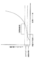
F=1/(2π√(L・C))
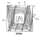
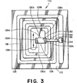
に従ってインダクタンス値およびキャパシタンス値により定められる。共振回路のインダクタンスを一定に維持してキャパシタンスを増加させると、周波数は減少し、インダクタンスを一定に維持してキャパシタンスを減少させると、共振周波数は増加する。第1導体パターン118上の第2導体パターン120の接着位置を正確に選択することにより、共振回路の共振周波数は、非常に厳密な許容範囲で所定の目標共振周波数に一致するよう、正確に制御し、または調整することが可能となる。
所定周波数または所定周波数の僅かな許容範囲内で共振する、共振周波数タグの作成方法の提供に加えて、本発明は、周波数領域内で、各々が異なる周波数で共振する、一連の他とは異なる別個の共振周波数タグを作成する方法も含んでいる。上記の説明により明確に理解可能なように、共振周波数タグの周波数は、タグのキャパシタンスとインダクタンスの逆関数であり、すでに説明した式により規定される。また、上述したように、図3に示した共振周波数タグでは、インダクタンスが一定であり、第1導体パターン118の誘導コイル126のサイズおよび他の特性により決定される。このようにして、図3のタグ110の周波数は、容量要素のキャパシタンスを規定する、第2導体パターン120の位置により規定されるタグのキャパシタンス、特に、導体ランド130により重なり合う導体ランド128の部分により決定される。第2導体パターン120、および特に導体ランド130が、第1導体ランド128の第1終端128aに向かって移動するにつれ、共振周波数回路のキャパシタンスは増加し、それにより、周波数は低くなり、逆もまた同様である。
Claims (24)
- (a)誘導要素と第1ランドとを含む第1導体パターンを形成するステップであって、第1ランドは、誘導要素の1つの終端に接続された第1終端および所定の距離だけ第1終端から離れた第2終端を有する、ステップと、
(b)所定の幅を有する第2ランドおよびリンク要素を含む第2導体パターンを別個に形成するステップと、
(c)誘導要素と共に共振回路を形成する、第1の所定キャパシタンスを有する容量要素のプレートを構築するために、誘電体を介在させて、第2ランドが第1ランドの少なくとも一部分と重なるよう、第2導体パターンを第1導体パターンの近傍の第1所定位置へ配置するステップと、
(d)共振回路の共振周波数を測定し、測定周波数を所定周波数と比較するステップと、
(e)共振周波数が選択許容範囲内で所定周波数に合致しないなら、第1ランドの長さに沿って第2ランドが移動するよう、第2導体パターンを動かし、それにより容量要素のキャパシタンスを変更するステップと、
(f)ステップ(d)、(e)を、合致するまで繰り返すステップと、
(g)第1導体パターンへ第2導体パターンを固定するステップと
を含む、所定周波数で共振する共振周波数タグの作成方法。 - 第1ランドが、一方の終端から他方の終端へ、長さに沿って移動するにつれ、減少する幅を有している、請求項1に記載の方法。
- 第2ランドが、概して長方形であり、第1ランドの最大幅を超える長さを有している、請求項1に記載の方法。
- 第2導体パターンが、接着剤およびホットプレス法のうちの1つにより、第1導体パターンに固定される、請求項1に記載の方法。
- 第2導体パターンが、圧力を加えることにより第1導体パターンに固定され、加えられる圧力の量が、タグの共振周波数を制御するために変更される、請求項4に記載の方法。
- いったん形成された第2導体パターンが、初期にキャリヤーシート上に保持されている、請求項1に記載の方法。
- 第2導体パターンを第1導体パターンへ固定する前に第2ランドと第1ランドとの間に配置される誘電体層を、第2導体パターンが含んでいる、請求項1に記載の方法。
- リンク要素が、第2ランドへ接続された第1セクションおよび第2セクションを含み、リンク要素の第1および第2セクションが、所定の最小幅の隙間だけ距離を置いて離れており、さらに、少なくとも、リンク要素の第1セクションへ電気的に接続した第1リードと、リンク要素の第2セクションへ電気的に接続した第2リードを含む集積回路を含んでいる、請求項1に記載の方法。
- 集積回路が、リンク要素の第1セクションおよび第2セクションの一方へ固定されている、請求項8に記載の方法。
- (a)一連の第1導体パターンを形成するステップであって、第1導体パターンは全て実質的に同じであり、各第1導体パターンは、誘導要素ならびに第1ランドを含み、第1ランドは誘導要素の1つの終端に接続された第1終端、および第1終端から所定の距離だけ離れた第2終端を含んでいるステップと、
(b)別個に、一連の第2導体パターンを形成するステップであって、第2導体パターンは、全て実質的に同じであり、さらに、各第2導体パターンは、所定の幅を有する第2ランドおよびリンク要素を含む、ステップと、
(c)連続する第1タグの、第1所定キャパシタンスを有する容量要素のプレートを構築するために、誘電体を介在させて、第2ランドが第1ランドの少なくとも一部分と重なるよう、第2導体パターンを第1所定位置で連続する第1導体パターンへ固定するステップと、
(d)タグの共振周波数を測定して、測定周波数を所定周波数と比較するステップと、
(e)測定された共振周波数が選択許容範囲内で所定周波数に合致するなら、続くタグの、第1の所定キャパシタンスを有する容量要素のプレートを構築するために、誘電体を介在させて、第2ランドが第1ランドの少なくとも一部分と重なるよう、第2導体パターンをそれに続いて連続する第1導体パターンへ第1所定位置で固定し、その後、連続する残りに対して、ステップ(d)、(e)を繰り返し、さらに、共振周波数が選択許容範囲内で所定周波数に合致しないなら、続くタグの第2所定キャパシタンスを有する容量要素のプレートを構築するために、誘電体を介在させて、第2ランドが第1ランドの少なくとも一部分と重なるよう、第1所定位置とは異なる第2所定位置で、第2導体パターンをそれに続いて連続する第1導体パターンへ固定し、その後、連続する残りに対して、ステップ(d)、(e)を繰り返すステップと
を含む、実質的に同じ所定周波数で各々が共振する、一連の共振周波数タグの作成方法。 - 各第1ランドが、一方の終端から他方の終端へ、長さに沿って移動するにつれ、減少する幅を有する、請求項10に記載の方法。
- 各第2ランドが概して長方形であり、第1ランドの最大幅を超える長さを有する、請求項11に記載の方法。
- 各第2導体パターンが、接着剤およびホットプレス法のうちの1つにより、第1導体パターンに固定される、請求項10に記載の方法。
- 各第2導体パターンが、圧力を加えることにより対応する第1導体パターンに固定され、加えられる圧力の量が、各タグの共振周波数を制御するために変更される、請求項13に記載の方法。
- いったん形成された第2導体パターンが、初期にキャリヤーシート上に保持されている、請求項10に記載の方法。
- 第2導体パターンを対応する第1導体パターンへ固定する前に、第2ランドと第1ランドとの間に配置される誘電体層を、各第2導体パターンが含んでいる、請求項10に記載の方法。
- 各リンク要素が、第2ランドへ接続された第1セクションおよび第2セクションを含み、各リンク要素の第1セクションおよび第2セクションが、所定の最小幅のギャップだけ距離を置いて離れており、さらに、少なくとも、各リンク要素の第1セクションへ電気的に接続した第1リードと、リンク要素の第2セクションへ電気的に接続した第2リードを含む集積回路を含んでいる、請求項10に記載の方法。
- 集積回路が、各リンク要素の第1セクションおよび第2セクションの一方へ固定されている、請求項17に記載の方法。
- 一連のN個の共振周波数タグの作成方法であって、Nは1より大きな整数であり、N個のタグの各々は、連続した他のあらゆるタグの共振周波数と、少なくとも所定の最小周波数範囲だけ異なる共振周波数を有しており、前記方法は、
(a)N個の第1導体パターンを形成するステップであって、第1導体パターンは全て実質的に同じであり、各第1導体パターンは、誘導要素ならびに第1ランドを含み、第1ランドの第1終端は誘導要素の1つの終端に接続され、第1ランドの第2終端は第1終端から所定の距離だけ離れている、ステップと、
(b)別個に、N個の第2導体パターンを形成するステップであって、第2導体パターンは、全て実質的に同じであり、各第2導体パターンは、所定の幅を有する第2ランドおよびリンク要素を含む、ステップと、
(c)各共振周波数タグに対する容量要素のプレートを構築するために、誘電体を介在させて、各第2導体パターンの第2ランドが対応する第1導体パターンの第1ランドの一部分と重なるよう、第2導体パターンを、ある位置で第1導体パターンの各々へ連続して固定し、対応する第1導体パターンの第1ランドに対する各第2導体パターンの位置、したがって、第1ランドに各第2ランドが重なる量が、連続する共振周波数タグの各々で異なっており、各共振周波数タグが連続する他のあらゆる共振周波数タグと異なる周波数で共振するよう、各共振周波数タグの容量要素のキャパシタンスが、連続する他のあらゆる共振周波数タグの容量要素のキャパシタンスと、少なくとも最小値だけ異なるステップと
を含む、一連のN個の共振周波数タグの作成方法。 - 各第1ランドが、一方の終端から他方の終端へ、長さに沿って移動するにつれ、減少する幅を有する、請求項19に記載の方法。
- 各第2導体パターンが、接着剤およびホットプレス法のうちの1つにより、対応する第1導体パターンに固定される、請求項19に記載の方法。
- 各第2導体パターンが、圧力を加えることにより対応する第1導体パターンに固定され、加えられる圧力の量が、各タグの共振周波数を制御するために変更される、請求項21に記載の方法。
- いったん形成された第2導体パターンが、初期にキャリヤーシート上に保持されている、請求項19に記載の方法。
- 第2導体パターンを対応する基板へ固定する前に、第2ランドと第1ランドとの間に配置される誘電体層を、第2導体パターンが含んでいる、請求項19に記載の方法。
Applications Claiming Priority (2)
| Application Number | Priority Date | Filing Date | Title |
|---|---|---|---|
| US10/388,344 US6925701B2 (en) | 2003-03-13 | 2003-03-13 | Method of making a series of resonant frequency tags |
| PCT/US2004/001849 WO2004084119A2 (en) | 2003-03-13 | 2004-01-23 | Resonant frequency tag and method for controlling tag frequency |
Publications (2)
| Publication Number | Publication Date |
|---|---|
| JP2006521632A JP2006521632A (ja) | 2006-09-21 |
| JP4199801B2 true JP4199801B2 (ja) | 2008-12-24 |
Family
ID=32962106
Family Applications (1)
| Application Number | Title | Priority Date | Filing Date |
|---|---|---|---|
| JP2006508623A Expired - Fee Related JP4199801B2 (ja) | 2003-03-13 | 2004-01-23 | 共振周波数タグ、および共振周波数タグの制御方法 |
Country Status (14)
| Country | Link |
|---|---|
| US (3) | US6925701B2 (ja) |
| EP (3) | EP1933285B1 (ja) |
| JP (1) | JP4199801B2 (ja) |
| KR (1) | KR100744714B1 (ja) |
| CN (1) | CN100495452C (ja) |
| AR (1) | AR043264A1 (ja) |
| AT (3) | ATE389221T1 (ja) |
| AU (1) | AU2004222610B2 (ja) |
| CA (2) | CA2519104A1 (ja) |
| DE (3) | DE602004018754D1 (ja) |
| ES (2) | ES2320887T3 (ja) |
| MX (1) | MXPA05009780A (ja) |
| TW (1) | TW200426696A (ja) |
| WO (1) | WO2004084119A2 (ja) |
Families Citing this family (80)
| Publication number | Priority date | Publication date | Assignee | Title |
|---|---|---|---|---|
| ATE474287T1 (de) | 2002-04-24 | 2010-07-15 | Mineral Lassen Llc | Herstellungsverfahren für eine drahtlose kommunikationsvorrichtung und herstellungsvorrichtung |
| JP2004284601A (ja) * | 2003-03-19 | 2004-10-14 | Renesas Technology Corp | 半導体装置の搬送方法および実装方法ならびに包装方法およびそれに用いられる収容体の再利用方法 |
| WO2004094012A2 (en) * | 2003-04-17 | 2004-11-04 | Alliance Gaming Corporation | Wireless monitoring of playing cards and/or wagers in gaming |
| US7324061B1 (en) | 2003-05-20 | 2008-01-29 | Alien Technology Corporation | Double inductor loop tag antenna |
| US7253497B2 (en) | 2003-07-02 | 2007-08-07 | Lsi Corporation | Integrated circuit with inductor having horizontal magnetic flux lines |
| US7753798B2 (en) * | 2003-09-05 | 2010-07-13 | Bally Gaming International, Inc. | Systems, methods, and devices for monitoring card games, such as baccarat |
| US7158037B2 (en) * | 2004-03-22 | 2007-01-02 | Avery Dennison Corporation | Low cost method of producing radio frequency identification tags with straps without antenna patterning |
| ITMO20040080A1 (it) * | 2004-04-08 | 2004-07-08 | Windinglab S R L | Metodo di realizzazione di un circuito stampato di spessore sottile e circuito relativo |
| US7292148B2 (en) * | 2004-06-18 | 2007-11-06 | Avery Dennison Corporation | Method of variable position strap mounting for RFID transponder |
| JP4649183B2 (ja) * | 2004-11-30 | 2011-03-09 | 株式会社東芝 | 無線通信端末 |
| GB0501199D0 (en) * | 2005-01-21 | 2005-03-02 | Qinetiq Ltd | Improved RF tags |
| US7477152B2 (en) | 2005-03-14 | 2009-01-13 | Avery Dennison Corporation | RFID application test systems and methods |
| US7411498B2 (en) | 2005-04-07 | 2008-08-12 | Avery Dennison | RFID testing and classification systems and methods |
| US7295117B2 (en) | 2005-04-07 | 2007-11-13 | Avery Dennison | RFID device test thresholds systems and methods |
| US20060238989A1 (en) * | 2005-04-25 | 2006-10-26 | Delaware Capital Formation, Inc. | Bonding and protective method and apparatus for RFID strap |
| US7298266B2 (en) | 2005-05-09 | 2007-11-20 | Avery Dennison | RFID communication systems and methods |
| US7298267B2 (en) | 2005-05-09 | 2007-11-20 | Avery Dennison | RFID test interface systems and methods |
| US7359823B2 (en) | 2005-05-25 | 2008-04-15 | Avery Dennison | RFID device variable test systems and methods |
| JP4629535B2 (ja) * | 2005-08-30 | 2011-02-09 | 大日本印刷株式会社 | 非接触データキャリア用部材の製造方法及び成形型 |
| US20070046469A1 (en) * | 2005-09-01 | 2007-03-01 | Mark Pempsell | Electronic Deactivation Device for RFID Surveillance and Storage |
| US8550464B2 (en) | 2005-09-12 | 2013-10-08 | Bally Gaming, Inc. | Systems, methods and articles to facilitate playing card games with selectable odds |
| US20070262866A1 (en) * | 2005-11-14 | 2007-11-15 | Ronald Eveland | Multi-Dimensional Broadband Track and Trace Sensor Radio Frequency Identification Device |
| US20070229264A1 (en) * | 2005-11-14 | 2007-10-04 | Ronald Eveland | Software method and system for encapsulation of RFID data into a standardized globally routable format |
| US20070115130A1 (en) * | 2005-11-14 | 2007-05-24 | Ronald Eveland | Multi-dimensional, broadband track and trace sensor radio frequency identification device |
| US8067253B2 (en) * | 2005-12-21 | 2011-11-29 | Avery Dennison Corporation | Electrical device and method of manufacturing electrical devices using film embossing techniques to embed integrated circuits into film |
| DE102006001504A1 (de) * | 2006-01-11 | 2007-07-12 | Infineon Technologies Ag | Identifikations-Datenträger, Lese-Vorrichtung, Identifikations-System und Verfahren zum Herstellen eines Identifikations-Datenträgers |
| US8786510B2 (en) * | 2006-01-24 | 2014-07-22 | Avery Dennison Corporation | Radio frequency (RF) antenna containing element and methods of making the same |
| JP2007235926A (ja) * | 2006-01-31 | 2007-09-13 | Toshiba Tec Corp | 無線icタグ |
| US20070194927A1 (en) * | 2006-02-15 | 2007-08-23 | Johannes Maximilian Peter | Electronic article surveillance marker |
| US7653823B2 (en) * | 2006-03-20 | 2010-01-26 | Lenovo (Singapore) Pte. Ltd. | Method and apparatus for informing computer of power environment |
| US7646304B2 (en) * | 2006-04-10 | 2010-01-12 | Checkpoint Systems, Inc. | Transfer tape strap process |
| US8038153B2 (en) | 2006-05-23 | 2011-10-18 | Bally Gaming, Inc. | Systems, methods and articles to facilitate playing card games |
| US7753779B2 (en) | 2006-06-16 | 2010-07-13 | Bally Gaming, Inc. | Gaming chip communication system and method |
| DE102006028827A1 (de) * | 2006-06-21 | 2008-01-10 | Dynamic Systems Gmbh | Transponder mit elektronischem Speicherchip und magnetischer Ringantenne |
| US20080018473A1 (en) * | 2006-07-18 | 2008-01-24 | 3M Innovative Properties Company | Electrostatic discharge protection for components of an rfid tag |
| US7791445B2 (en) * | 2006-09-12 | 2010-09-07 | Cooper Technologies Company | Low profile layered coil and cores for magnetic components |
| US7784429B2 (en) * | 2006-09-22 | 2010-08-31 | Chiodo Chris D | Contoured specimen holder for imaging machines |
| US8647191B2 (en) | 2006-09-26 | 2014-02-11 | Bally Gaming, Inc. | Resonant gaming chip identification system and method |
| KR100776679B1 (ko) * | 2006-09-27 | 2007-11-16 | 한국전자통신연구원 | 챔버의 비운용 주파수 대역에서의 안테나 특성 측정 방법 |
| US8179231B1 (en) * | 2006-09-28 | 2012-05-15 | Louisiana Tech Research Foundation | Transmission delay based RFID tag |
| AT504243B1 (de) * | 2006-10-11 | 2011-02-15 | Evva Sicherheitstechnologie | Verfahren zur herstellung eines identifikationsträgers oder elektronischen schlüssels für elektronisch betätigbare schlösser |
| US9658178B2 (en) | 2012-09-28 | 2017-05-23 | General Electric Company | Sensor systems for measuring an interface level in a multi-phase fluid composition |
| US9536122B2 (en) | 2014-11-04 | 2017-01-03 | General Electric Company | Disposable multivariable sensing devices having radio frequency based sensors |
| US9389296B2 (en) * | 2012-07-26 | 2016-07-12 | General Electric Company | Method for sensor reader calibration |
| US10914698B2 (en) | 2006-11-16 | 2021-02-09 | General Electric Company | Sensing method and system |
| US9589686B2 (en) | 2006-11-16 | 2017-03-07 | General Electric Company | Apparatus for detecting contaminants in a liquid and a system for use thereof |
| US9538657B2 (en) | 2012-06-29 | 2017-01-03 | General Electric Company | Resonant sensor and an associated sensing method |
| CN101197462B (zh) * | 2006-12-07 | 2011-05-25 | 上海英内电子标签有限公司 | Rfid蚀刻铝天线的制造方法 |
| DE102006061798A1 (de) * | 2006-12-21 | 2008-06-26 | Simons, Gisela | Verfahren zur Anbringung von Kennzeichen auf Substratoberflächen mit Hilfe eines Transferverfahrens |
| JP2008165678A (ja) | 2007-01-04 | 2008-07-17 | Lintec Corp | Icチップ実装用接続体、アンテナ回路、icインレット、icタグ及び静電容量調整方法 |
| US8009101B2 (en) * | 2007-04-06 | 2011-08-30 | Murata Manufacturing Co., Ltd. | Wireless IC device |
| US8102276B2 (en) * | 2007-08-31 | 2012-01-24 | Pathfinder Energy Sevices, Inc. | Non-contact capacitive datalink for a downhole assembly |
| US8920236B2 (en) | 2007-11-02 | 2014-12-30 | Bally Gaming, Inc. | Game related systems, methods, and articles that combine virtual and physical elements |
| US9005034B2 (en) | 2008-04-30 | 2015-04-14 | Bally Gaming, Inc. | Systems and methods for out-of-band gaming machine management |
| EP2128587B1 (en) * | 2008-05-28 | 2018-11-07 | EADS Deutschland GmbH | Irregularity detection in a structure of an aircraft |
| KR101270543B1 (ko) * | 2008-12-03 | 2013-06-03 | 삼성전자주식회사 | 메타물질을 이용한 칩리스 알에프 아이디 시스템 및 그 인식 방법 |
| US20100224356A1 (en) * | 2009-03-06 | 2010-09-09 | Smith International, Inc. | Apparatus for electrical power and/or data transfer between rotating components in a drill string |
| US8701271B2 (en) * | 2010-04-14 | 2014-04-22 | Avery Dennison Corporation | Method of assembly of articles |
| EP2580715B1 (en) | 2010-06-14 | 2019-05-22 | Avery Dennison Corporation | Method, system and apparatus for making short run radio frequency identification tags and labels |
| US9643056B2 (en) | 2010-08-18 | 2017-05-09 | Edge Technology | Golf ball with RFID inlay between a split core |
| US9370694B2 (en) * | 2010-08-18 | 2016-06-21 | Edge Technology | Golf ball with RFID inlay in a molded impression |
| US8542023B2 (en) | 2010-11-09 | 2013-09-24 | General Electric Company | Highly selective chemical and biological sensors |
| EP2493017A1 (de) * | 2011-02-28 | 2012-08-29 | Felix Schoeller Supply Chain Technologies GmbH & Co. KG | Verfahren zur Herstellung einer Antennenanordnung |
| FI125720B (fi) | 2011-05-19 | 2016-01-29 | Tecnomar Oy | Rullalta rullalle -massavalmistukseen soveltuva sähköisten siltojen valmistusmenetelmä |
| EP2645298A1 (en) * | 2012-03-30 | 2013-10-02 | austriamicrosystems AG | Portable object and information transmission system |
| US20130330638A1 (en) * | 2012-06-12 | 2013-12-12 | GM Global Technology Operations LLC | Coated substrate and product including the same and methods of making and using the same |
| AT512401B1 (de) * | 2012-08-06 | 2013-08-15 | Seibersdorf Labor Gmbh | Behälter mit Füllstandsüberwachung |
| US10598650B2 (en) | 2012-08-22 | 2020-03-24 | General Electric Company | System and method for measuring an operative condition of a machine |
| DE112013004129T5 (de) | 2012-08-22 | 2015-05-21 | General Electric Company | Drahtloses System und Verfahren zum Messen einer Betriebsbedingung einer Maschine |
| JP5969339B2 (ja) * | 2012-09-21 | 2016-08-17 | トッパン・フォームズ株式会社 | 周波数調整方法 |
| JP2014063368A (ja) * | 2012-09-21 | 2014-04-10 | Toppan Forms Co Ltd | 周波数調整方法及びこれを用いて製造されたrf−idメディア |
| US10684268B2 (en) | 2012-09-28 | 2020-06-16 | Bl Technologies, Inc. | Sensor systems for measuring an interface level in a multi-phase fluid composition |
| US8990744B2 (en) * | 2013-04-16 | 2015-03-24 | Infineon Technologies Ag | Electrical measurement based circuit wiring layout modification method and system |
| TWI509523B (zh) * | 2013-06-11 | 2015-11-21 | China Steel Corp | 無線射頻標籤及其操作頻率之調整方法 |
| KR101424688B1 (ko) * | 2014-02-18 | 2014-08-04 | (주) 성수기전 | 루프안테나 제조 방법 |
| WO2015141016A1 (ja) * | 2014-03-17 | 2015-09-24 | 株式会社村田製作所 | アンテナ装置、無線通信端末 |
| JP5673891B1 (ja) * | 2014-03-17 | 2015-02-18 | 株式会社村田製作所 | アンテナ装置、無線通信端末 |
| CN108282169A (zh) * | 2018-01-31 | 2018-07-13 | 上海康斐信息技术有限公司 | 一种易于调试的射频匹配结构和射频匹配电路 |
| CN111091966B (zh) * | 2020-01-04 | 2021-04-16 | 深圳感通科技有限公司 | 一体成型电感的自动绕制生产工艺 |
| US11068674B1 (en) * | 2021-02-15 | 2021-07-20 | King Abdulaziz University | RFID tag identification methods, devices, and algorithms based on eigen-mode technique |
Family Cites Families (22)
| Publication number | Priority date | Publication date | Assignee | Title |
|---|---|---|---|---|
| US3863244A (en) | 1972-06-14 | 1975-01-28 | Lichtblau G J | Electronic security system having improved noise discrimination |
| US3913219A (en) * | 1974-05-24 | 1975-10-21 | Lichtblau G J | Planar circuit fabrication process |
| US4369557A (en) * | 1980-08-06 | 1983-01-25 | Jan Vandebult | Process for fabricating resonant tag circuit constructions |
| DE3221500A1 (de) * | 1982-06-07 | 1983-12-08 | Max-E. Dipl.-Ing. 7320 Göppingen Reeb | Identifizierungsanordnung in form eines an einem gegenstand anbringbaren gebildes und verfahren zur herstellung |
| US4717438A (en) * | 1986-09-29 | 1988-01-05 | Monarch Marking Systems, Inc. | Method of making tags |
| JPH0780386B2 (ja) * | 1989-01-25 | 1995-08-30 | 東海金属株式会社 | 共振タグおよびその製造方法 |
| JP3096069B2 (ja) * | 1990-08-06 | 2000-10-10 | チェックポイント・マニュファクチュアリング・ジャパン株式会社 | 共振タグ及びその製造方法 |
| US5182544A (en) * | 1991-10-23 | 1993-01-26 | Checkpoint Systems, Inc. | Security tag with electrostatic protection |
| US5276431A (en) * | 1992-04-29 | 1994-01-04 | Checkpoint Systems, Inc. | Security tag for use with article having inherent capacitance |
| US5381137A (en) * | 1992-10-26 | 1995-01-10 | Motorola, Inc. | RF tagging system and RF tags and method |
| US5444223A (en) * | 1994-01-11 | 1995-08-22 | Blama; Michael J. | Radio frequency identification tag and method |
| US5754431A (en) * | 1995-09-18 | 1998-05-19 | Shima Seiki Manufacturing, Ltd. | Method and apparatus for designing a tubular knitted fabric using a flat knitting machine |
| US5754110A (en) * | 1996-03-07 | 1998-05-19 | Checkpoint Systems, Inc. | Security tag and manufacturing method |
| US6133834A (en) * | 1997-03-06 | 2000-10-17 | Texas Instruments Deutschland, Gmbh | Method of trimming film type antennas |
| US5841350A (en) * | 1997-06-27 | 1998-11-24 | Checkpoint Systems, Inc. | Electronic security tag useful in electronic article indentification and surveillance system |
| US5861809A (en) * | 1997-09-22 | 1999-01-19 | Checkpoint Systems, Inc. | Deactivateable resonant circuit |
| US6087940A (en) * | 1998-07-28 | 2000-07-11 | Novavision, Inc. | Article surveillance device and method for forming |
| WO2000079497A1 (en) * | 1999-06-21 | 2000-12-28 | Bent Thorning Bensen A/S | Radiofrequency resonant circuit sensing device, method of its production, and uses |
| FR2802000B1 (fr) * | 1999-12-01 | 2002-03-22 | Gemplus Card Int | Procede de realisation d'un circuit oscillant accorde et fabrication de dispositifs de radiocommunications de faibles dimensions comprenant un tel circuit |
| US6400271B1 (en) * | 2000-03-20 | 2002-06-04 | Checkpoint Systems, Inc. | Activate/deactiveable security tag with enhanced electronic protection for use with an electronic security system |
| JP2002259926A (ja) * | 2001-03-05 | 2002-09-13 | Miyake:Kk | 折り曲げ共振回路及びその取付け方法 |
| JP4794742B2 (ja) * | 2001-03-13 | 2011-10-19 | 太平洋セメント株式会社 | 圧電トランス |
-
2003
- 2003-03-13 US US10/388,344 patent/US6925701B2/en not_active Expired - Fee Related
-
2004
- 2004-01-23 CA CA002519104A patent/CA2519104A1/en not_active Abandoned
- 2004-01-23 AT AT07005825T patent/ATE389221T1/de not_active IP Right Cessation
- 2004-01-23 WO PCT/US2004/001849 patent/WO2004084119A2/en active IP Right Grant
- 2004-01-23 ES ES04704904T patent/ES2320887T3/es not_active Expired - Lifetime
- 2004-01-23 AT AT08153072T patent/ATE452394T1/de not_active IP Right Cessation
- 2004-01-23 DE DE602004018754T patent/DE602004018754D1/de not_active Expired - Fee Related
- 2004-01-23 CN CNB2004800129106A patent/CN100495452C/zh not_active Expired - Fee Related
- 2004-01-23 JP JP2006508623A patent/JP4199801B2/ja not_active Expired - Fee Related
- 2004-01-23 EP EP08153072A patent/EP1933285B1/en not_active Expired - Lifetime
- 2004-01-23 EP EP07005825A patent/EP1798697B1/en not_active Expired - Lifetime
- 2004-01-23 DE DE602004024725T patent/DE602004024725D1/de not_active Expired - Fee Related
- 2004-01-23 EP EP04704904A patent/EP1602089B1/en not_active Expired - Lifetime
- 2004-01-23 MX MXPA05009780A patent/MXPA05009780A/es active IP Right Grant
- 2004-01-23 CA CA002672690A patent/CA2672690A1/en not_active Abandoned
- 2004-01-23 AT AT04704904T patent/ATE419602T1/de not_active IP Right Cessation
- 2004-01-23 DE DE602004012464T patent/DE602004012464T2/de not_active Expired - Fee Related
- 2004-01-23 AU AU2004222610A patent/AU2004222610B2/en not_active Ceased
- 2004-01-23 ES ES07005825T patent/ES2303334T3/es not_active Expired - Lifetime
- 2004-01-23 KR KR1020057017127A patent/KR100744714B1/ko not_active IP Right Cessation
- 2004-01-30 TW TW093102161A patent/TW200426696A/zh unknown
- 2004-02-23 AR ARP040100562A patent/AR043264A1/es unknown
- 2004-10-19 US US10/968,387 patent/US7076858B2/en not_active Expired - Fee Related
- 2004-10-19 US US10/967,947 patent/US7168150B2/en not_active Expired - Fee Related
Also Published As
Similar Documents
| Publication | Publication Date | Title |
|---|---|---|
| JP4199801B2 (ja) | 共振周波数タグ、および共振周波数タグの制御方法 | |
| US7646305B2 (en) | Capacitor strap | |
| US7492164B2 (en) | Method for manufacturing a product sensor, and a product sensor | |
| FI113809B (fi) | Menetelmä älytarran valmistamiseksi sekä älytarra | |
| JP2018206242A (ja) | 非接触icカード用インレット、非接触icカード及び非接触icカードの共振周波数調整方法 | |
| JP2007515006A (ja) | セキュリティ用レゾナンスタグおよびセキュリティ用レゾナンスタグの製造方法 |
Legal Events
| Date | Code | Title | Description |
|---|---|---|---|
| RD03 | Notification of appointment of power of attorney |
Free format text: JAPANESE INTERMEDIATE CODE: A7423 Effective date: 20080128 |
|
| A977 | Report on retrieval |
Free format text: JAPANESE INTERMEDIATE CODE: A971007 Effective date: 20080903 |
|
| TRDD | Decision of grant or rejection written | ||
| A01 | Written decision to grant a patent or to grant a registration (utility model) |
Free format text: JAPANESE INTERMEDIATE CODE: A01 Effective date: 20080909 |
|
| A01 | Written decision to grant a patent or to grant a registration (utility model) |
Free format text: JAPANESE INTERMEDIATE CODE: A01 |
|
| A61 | First payment of annual fees (during grant procedure) |
Free format text: JAPANESE INTERMEDIATE CODE: A61 Effective date: 20081003 |
|
| FPAY | Renewal fee payment (event date is renewal date of database) |
Free format text: PAYMENT UNTIL: 20111010 Year of fee payment: 3 |
|
| R150 | Certificate of patent or registration of utility model |
Free format text: JAPANESE INTERMEDIATE CODE: R150 |
|
| FPAY | Renewal fee payment (event date is renewal date of database) |
Free format text: PAYMENT UNTIL: 20121010 Year of fee payment: 4 |
|
| FPAY | Renewal fee payment (event date is renewal date of database) |
Free format text: PAYMENT UNTIL: 20131010 Year of fee payment: 5 |
|
| R250 | Receipt of annual fees |
Free format text: JAPANESE INTERMEDIATE CODE: R250 |
|
| R250 | Receipt of annual fees |
Free format text: JAPANESE INTERMEDIATE CODE: R250 |
|
| R250 | Receipt of annual fees |
Free format text: JAPANESE INTERMEDIATE CODE: R250 |
|
| R250 | Receipt of annual fees |
Free format text: JAPANESE INTERMEDIATE CODE: R250 |
|
| LAPS | Cancellation because of no payment of annual fees |