JP4178890B2 - Solid-state imaging device - Google Patents
Solid-state imaging device Download PDFInfo
- Publication number
- JP4178890B2 JP4178890B2 JP2002260417A JP2002260417A JP4178890B2 JP 4178890 B2 JP4178890 B2 JP 4178890B2 JP 2002260417 A JP2002260417 A JP 2002260417A JP 2002260417 A JP2002260417 A JP 2002260417A JP 4178890 B2 JP4178890 B2 JP 4178890B2
- Authority
- JP
- Japan
- Prior art keywords
- solid
- imaging device
- state imaging
- electrode pad
- curved
- Prior art date
- Legal status (The legal status is an assumption and is not a legal conclusion. Google has not performed a legal analysis and makes no representation as to the accuracy of the status listed.)
- Expired - Fee Related
Links
- 238000003384 imaging method Methods 0.000 title claims description 176
- 238000000034 method Methods 0.000 description 16
- 230000004075 alteration Effects 0.000 description 11
- 238000004519 manufacturing process Methods 0.000 description 11
- 230000003287 optical effect Effects 0.000 description 10
- 238000010586 diagram Methods 0.000 description 5
- 238000005452 bending Methods 0.000 description 4
- 238000005498 polishing Methods 0.000 description 4
- 230000002093 peripheral effect Effects 0.000 description 3
- 239000004065 semiconductor Substances 0.000 description 3
- 239000000758 substrate Substances 0.000 description 3
- 238000004891 communication Methods 0.000 description 2
- 238000005336 cracking Methods 0.000 description 2
- 230000000694 effects Effects 0.000 description 2
- 239000011521 glass Substances 0.000 description 2
- 239000000126 substance Substances 0.000 description 2
- 229910010293 ceramic material Inorganic materials 0.000 description 1
- 239000006059 cover glass Substances 0.000 description 1
- 238000005520 cutting process Methods 0.000 description 1
- 230000006378 damage Effects 0.000 description 1
- 238000005516 engineering process Methods 0.000 description 1
- 239000002184 metal Substances 0.000 description 1
- 239000007787 solid Substances 0.000 description 1
- 239000010409 thin film Substances 0.000 description 1
Images


Classifications
-
- H—ELECTRICITY
- H01—ELECTRIC ELEMENTS
- H01L—SEMICONDUCTOR DEVICES NOT COVERED BY CLASS H10
- H01L2224/00—Indexing scheme for arrangements for connecting or disconnecting semiconductor or solid-state bodies and methods related thereto as covered by H01L24/00
- H01L2224/01—Means for bonding being attached to, or being formed on, the surface to be connected, e.g. chip-to-package, die-attach, "first-level" interconnects; Manufacturing methods related thereto
- H01L2224/02—Bonding areas; Manufacturing methods related thereto
- H01L2224/04—Structure, shape, material or disposition of the bonding areas prior to the connecting process
- H01L2224/05—Structure, shape, material or disposition of the bonding areas prior to the connecting process of an individual bonding area
- H01L2224/0554—External layer
- H01L2224/0555—Shape
- H01L2224/05552—Shape in top view
- H01L2224/05554—Shape in top view being square
-
- H—ELECTRICITY
- H01—ELECTRIC ELEMENTS
- H01L—SEMICONDUCTOR DEVICES NOT COVERED BY CLASS H10
- H01L2224/00—Indexing scheme for arrangements for connecting or disconnecting semiconductor or solid-state bodies and methods related thereto as covered by H01L24/00
- H01L2224/01—Means for bonding being attached to, or being formed on, the surface to be connected, e.g. chip-to-package, die-attach, "first-level" interconnects; Manufacturing methods related thereto
- H01L2224/42—Wire connectors; Manufacturing methods related thereto
- H01L2224/44—Structure, shape, material or disposition of the wire connectors prior to the connecting process
- H01L2224/45—Structure, shape, material or disposition of the wire connectors prior to the connecting process of an individual wire connector
- H01L2224/45001—Core members of the connector
- H01L2224/45099—Material
- H01L2224/451—Material with a principal constituent of the material being a metal or a metalloid, e.g. boron (B), silicon (Si), germanium (Ge), arsenic (As), antimony (Sb), tellurium (Te) and polonium (Po), and alloys thereof
- H01L2224/45138—Material with a principal constituent of the material being a metal or a metalloid, e.g. boron (B), silicon (Si), germanium (Ge), arsenic (As), antimony (Sb), tellurium (Te) and polonium (Po), and alloys thereof the principal constituent melting at a temperature of greater than or equal to 950°C and less than 1550°C
- H01L2224/45144—Gold (Au) as principal constituent
-
- H—ELECTRICITY
- H01—ELECTRIC ELEMENTS
- H01L—SEMICONDUCTOR DEVICES NOT COVERED BY CLASS H10
- H01L2224/00—Indexing scheme for arrangements for connecting or disconnecting semiconductor or solid-state bodies and methods related thereto as covered by H01L24/00
- H01L2224/01—Means for bonding being attached to, or being formed on, the surface to be connected, e.g. chip-to-package, die-attach, "first-level" interconnects; Manufacturing methods related thereto
- H01L2224/42—Wire connectors; Manufacturing methods related thereto
- H01L2224/47—Structure, shape, material or disposition of the wire connectors after the connecting process
- H01L2224/48—Structure, shape, material or disposition of the wire connectors after the connecting process of an individual wire connector
- H01L2224/4805—Shape
- H01L2224/4809—Loop shape
- H01L2224/48091—Arched
-
- H—ELECTRICITY
- H01—ELECTRIC ELEMENTS
- H01L—SEMICONDUCTOR DEVICES NOT COVERED BY CLASS H10
- H01L2224/00—Indexing scheme for arrangements for connecting or disconnecting semiconductor or solid-state bodies and methods related thereto as covered by H01L24/00
- H01L2224/01—Means for bonding being attached to, or being formed on, the surface to be connected, e.g. chip-to-package, die-attach, "first-level" interconnects; Manufacturing methods related thereto
- H01L2224/42—Wire connectors; Manufacturing methods related thereto
- H01L2224/47—Structure, shape, material or disposition of the wire connectors after the connecting process
- H01L2224/48—Structure, shape, material or disposition of the wire connectors after the connecting process of an individual wire connector
- H01L2224/481—Disposition
- H01L2224/48151—Connecting between a semiconductor or solid-state body and an item not being a semiconductor or solid-state body, e.g. chip-to-substrate, chip-to-passive
- H01L2224/48221—Connecting between a semiconductor or solid-state body and an item not being a semiconductor or solid-state body, e.g. chip-to-substrate, chip-to-passive the body and the item being stacked
- H01L2224/48225—Connecting between a semiconductor or solid-state body and an item not being a semiconductor or solid-state body, e.g. chip-to-substrate, chip-to-passive the body and the item being stacked the item being non-metallic, e.g. insulating substrate with or without metallisation
- H01L2224/48227—Connecting between a semiconductor or solid-state body and an item not being a semiconductor or solid-state body, e.g. chip-to-substrate, chip-to-passive the body and the item being stacked the item being non-metallic, e.g. insulating substrate with or without metallisation connecting the wire to a bond pad of the item
-
- H—ELECTRICITY
- H01—ELECTRIC ELEMENTS
- H01L—SEMICONDUCTOR DEVICES NOT COVERED BY CLASS H10
- H01L2924/00—Indexing scheme for arrangements or methods for connecting or disconnecting semiconductor or solid-state bodies as covered by H01L24/00
- H01L2924/15—Details of package parts other than the semiconductor or other solid state devices to be connected
- H01L2924/151—Die mounting substrate
- H01L2924/1515—Shape
- H01L2924/15153—Shape the die mounting substrate comprising a recess for hosting the device
- H01L2924/15155—Shape the die mounting substrate comprising a recess for hosting the device the shape of the recess being other than a cuboid
- H01L2924/15156—Side view
Landscapes
- Solid State Image Pick-Up Elements (AREA)
- Transforming Light Signals Into Electric Signals (AREA)
- Studio Devices (AREA)
Description
【0001】
【発明の属する技術分野】
本発明は、固体撮像素子、この固体撮像素子を備えた固体撮像装置及び固体撮像装置の製造方法に関する。
【0002】
【従来の技術】
一般に固体撮像装置に用いられる固体撮像素子は、幾つもの半導体製造工程を経た半導体ウェハからダイシング法などにより各チップ状即ち個片に切断して分離される。このようにして得られた固体撮像素子は、平板状に形成されると共に、厚さが300μm程度あって、リジットな形状特性(堅くて変形しない特性)を有している。また、複数の固体撮像素子の主面に形成される撮像面は、この主面に沿って平面状態を有する形で配置されている。
【0003】
一方、固体撮像素子上(撮像面)で被写体を結像させるには、結像光学系が必要となる。結像光学系には結像レンズが組み込まれ、この結像レンズによって、固体撮像素子上に被写体が結像される。
【0004】
一般に、結像レンズで被写体を結像させた場合、像面湾曲と呼ばれるレンズ収差現象によって、撮像面の中心部と周辺部において焦点位置のずれが発生する。即ち、図14に示すように、固体撮像素子134上に、結像レンズ132と絞り131を備えた結像光学系133を配置した構成において、撮像面の中心部に焦点を合わせると、周辺部では空中で焦点を結ぶという不具合が生じる。その結果、画像の中心部と周辺部とで画質が不均一になるなど、撮像特性の劣化を招くことになる。
【0005】
このような不具合に対して結像レンズを複数枚組み合わせるなどの手段により、レンズ収差の補正を行っている。ただ、この結像レンズを複数枚組合せる方法では、結像レンズを含む結像光学系の設計に大きな負担が掛かることや、充分にレンズ収差を補正しきれないなどの理由によって、画質の劣化を招く恐れがあった。
【0006】
そこで、固体撮像素子を湾曲させた形状で固定することによって、結像光学系で発生するレンズ収差を補正する方法が、特開2001−156278,特開2001−284564において、提案されている。
【0007】
図8〜図10は、特開2001ー284564号に記載された固体撮像装置の例である。図8の固体撮像装置41は、保持部材42の上面に湾曲支持部(凸部)43を一体に形成し、この保持部材42に固体撮像素子44を撮像面が上向きとなるように保持して構成される。固体撮像素子44は、その形状的な可撓性により保持部材42の上面と湾曲支持部43にそれぞれ当接するようにして湾曲形状に保持される。
図9の固体撮像装置45は、保持部材42の上面に段状の凹部46を一体に形成し、その凹部底面46aと湾曲支持部となる保持部材42上面とに固体撮像素子44を当接させるようにして固体撮像素子44を湾曲形状に保持して構成される。
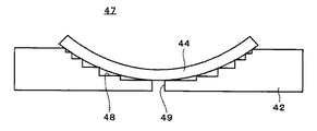
図10の固体撮像装置47は、保持部材42の凹部底面(階段状の包絡線が湾曲面)48に連通孔49を設けて置き、固体撮像素子44を保持部材42上に配置した状態で連通孔49からエアーを吸引することにより、固体撮像素子44を湾曲形状に保持して構成される。
【0008】
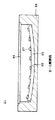
図11〜図12は、特開2001ー156278号に記載された固体撮像装置の例である。この固体撮像装置21は、所要の円筒面状の底面22を有するパッケージ23を設け、パッケージ23の底面22に沿うように撮像面24が上向きとなる湾曲形状の固体撮像素子25を配置し、パッケージ23の上部に透明ガラスカバー26を配置して構成される。固体撮像素子25は、平面からみて長方形をなし、長辺側が湾曲され、その湾曲した長辺側に沿って例えばAlによる電極パッド27が配列されている。この固体撮像素子25の電極パッド27に対応して、パッケージ23側の電極パッド31も長辺方向に配列され、互いに対応する電極パッド27と31間が例えばAu細線32によりワイヤーボンディングされて接続される。なお、図示せざるもパッケージ23の外側に電極パッド31と電気的に接続された外部リードが導出される。
【0009】
【発明が解決しようとする課題】
ところで、円筒面状または球面状に湾曲した固体撮像素子を固定した固体撮像装置においては、次のような問題点があった。
【0010】
上記の固体撮像素子は、例えば、撮像素子を作成した半導体基板(Si基板)の裏面を通常BGR(Back Grinder)と呼ばれている機械的研磨並びに化学的研磨法により、例えば、(30μm程度)の薄さに研磨することで可撓性を持たせて撮像面を湾曲させる。この湾曲した撮像面をパッケージ面に固定するとき、撮像面に歪み(うねり)が発生し、パッケージ面と固体撮像素子裏面との間にも、その歪み(うねり)による隙間が発生する。このため、超音波圧着法によるワイヤーボンディング時に超音波が拡散されてしまい、ボンディング不着が発生する。また、上記の隙間によって、ワイヤーボンディング時の超音波衝撃から電極パッドの剥れや割れなどを生じる。超音波の衝撃が大きい場合は、撮像素子の亀裂(割れ)に発展することも起こり得る。
【0011】
一方、通常の平板状の固体撮像素子の電極パッドへのAu細線のワイヤーボンディングは、各電極パッドの高さ位置が一定しているので、略均一な接合強度(シェア強度)を有している。しかし、湾曲した固体撮像素子の電極パッドへのワイヤーボンディングを通常のワイヤーボンディング装置を用いて行った場合、電極パッド27の傾斜角θ(図15参照)が徐々に変化するために、特に傾斜角θが大きくなる外側の電極パッド27とAu細線32間のシェア強度は許容値より低くなり、接続が不十分になることが判明した。また、各電極パッドの高さ位置が変化するので、電極パッドの位置認識が困難になり、安定したワイヤーボンディングが行い難い。
【0012】
本発明は、上述の点に鑑み、撮像面を円筒面状に湾曲した固体撮像素子の電極パッドへの電気的接続を安定して行えるようにし、品質の安定化、歩留りの向上を図った固体撮像素子、この固体撮像素子を備えた固体撮像装置及び固体撮像装置の製造方法を提供するものである。
【0013】
【課題を解決するための手段】
本発明に係る固体撮像素子は、少なくとも撮像面が円筒面状に湾曲され、電極パッドが湾曲されない方向に沿って配列された構成とする。固体撮像素子としては、撮像面を有する撮像チップ全体を円筒面状に湾曲させることができる。
【0014】
本発明の固体撮像素子においては、湾曲されていない水平方向に固体撮像素子の電極パッドを配列することにより、各電極パッドの高さ位置、傾斜角度が同じになり、各電極パッドに対して安定した電気的接続が可能になる。
【0015】
本発明に係る固体撮像装置は、少なくとも撮像面が円筒面状に湾曲され、電極パッドが湾曲されない方向に沿って配列された固体撮像素子を備え、この電極パッドに電気的接続がなされた構成とする。
本発明の固体撮像装置においては、固体撮像素子の電極パッドが湾曲されない方向に沿って配列されるので、各電極パッドの高さ位置、傾斜角度が同じになり、各電極パッドに対して安定した電気的接続が可能になる。従って、この種の固体撮像装置の高品質化、高歩留り化が可能になる。
【0016】
本発明に係る固体撮像装置の製造方法は、固体撮像素子の少なくとも撮像面を円筒面状に湾曲し、電極パッドを湾曲されない方向に沿って配列する工程を有する。
本発明に係る固体撮像装置の製造方法は、固体撮像素子の少なくとも撮像面を円筒面状に湾曲し、電極パッドを湾曲されない方向に沿って配列する工程と、固体撮像素子をパッケ−ジに収容する工程と、固体撮像素子の電極パッドとパッケージ側の電極パッドとを電気的に接続する工程とを有する。
本発明に係る固体撮像装置の製造方法は、固体撮像素子の少なくとも撮像面を円筒面状に湾曲し、電極パッドを湾曲されない方向に沿って配列する工程と、この電極パッドをTABボンディングで外部接続する工程とを有する。
本発明の固体撮像装置の製造方法においては、固体撮像素子の電極パッドを湾曲されない方向に沿って配列する工程を有するので、各電極パッドの高さ位置、傾斜角度を同じにすることができる。従って、その後の、固体撮像素子をパッケ−ジに収容して固体撮像素子の電極パッドとパッケージ側の電極パッドとの電気的接続工程、あるいはTABボンディングで外部接続する工程において、固体撮像素子の電極パッドに対して安定した電気的接続ができる。
【0017】
【発明の実施の形態】
以下、図面を参照して本発明の実施の形態を説明する。
【0018】
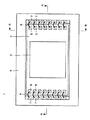
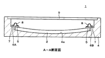
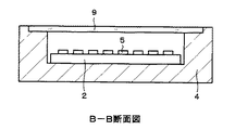
図1〜図3は、本発明に係る固体撮像装置及びその製造方法の一実施の形態を示す。本実施の形態に係る固体撮像装置1は、撮像面3を有し少なくとも撮像面3が円筒面状に湾曲した固体撮像素子2と、この固体撮像素子2を収容したパッケージ4とから構成される。本例の固体撮像素子2は、長方形をなす撮像チップの全体を長辺方向に沿って円筒面状に湾曲して構成される。この固体撮像素子2は、結像光学系で発生するレンズ収差(像面湾曲)を補正するように、所要の曲率の円筒面状に湾曲され、特に、複数の例えばAlによる電極パッド5が湾曲されない方向、即ち短辺方向に沿って配列されて成る。電極パッド5は撮像面3を挟んで両側に配置される。
【0019】
湾曲した固体撮像素子2は、例えば、基板裏面を化学的機械的研磨法(BGR法)等により可撓性を有する薄さ、例えば100μm以下、好ましくは50μm以下、さらに好ましくは20μm以下の厚みに形成し、撮像面3の端部と中央部との高さの差Δhが約100μm程度となるように円筒面状に湾曲して形成することができる。
【0020】
固体撮像素子2としては、例えばCCD撮像素子、CMOS撮像素子、その他等を適用することができる。
【0021】
パッケージ4は、例えばセラミック材からなり、固体撮像素子2を配置する底面4aの全体が固体撮像素子2と同じ曲率の円筒面状に形成さて成る。パッケージ4内の一方の相対向する両内側壁に段差部6〔6A,6B〕が形成され、この段差部6A,6Bの上面に夫々固体撮像素子2の電極パッド5と電気的に接続される例えばAlによる電極パッド7が形成される。なお、図示せざるもパッケージ4の外側には、電極パッド7と電気的に接続された外部リードが導出されている。
【0022】
固体撮像素子2は、その裏面を底面4aに当接するようにパッケージ4内の配置された状態で、金属細線、例えばAu細線8によるワイヤーボンディングにより、撮像素子2の電極パッド5とパッケージ4の電極パッド7間が電気的に接続される。そして、パッケージ4の上部が透明カバー部材、例えば平板状のカバーガラス9で封止される。
【0023】
本実施の形態によれば、円筒面状に湾曲された固体撮像素子2の電極パッド5のレイアウトを、湾曲されない方向、本例では短辺方向に配置することにより、各電極パッド5の高さ位置、傾斜角度が変化せず同一になり、各電極パッド5に対して同じ条件で容易に且つ安定したワイヤーボンディングを行うことができる。図2に示すように、電極パッド5も傾斜しているが、一定の条件で傾斜した電極パッド5に対して専用のボンディング条件を設定すれば、安定した規定以上のシェア強度が確保でき、良好なワイヤーボンディングができる。各電極パッド5の高さ位置が同じであるので、ボンディング時での電極パッドの位置認識も容易である。従って、従来の安価なワイヤーボンディング技術が使え、固体撮像装置としてコストダウンできると同時に安定した品質が確保できる。
【0024】
なお、従来のワイヤーボンディング装置を用いる以外に、一定に傾いた電極パッドに対してボンディング条件を設定した専用ワイヤーボンディング装置を用いることもできる。例えば傾斜した電極パッドを水平に見立ててキャピラリーを電極パッドに垂直に当てるような専用ワイヤーボンディング装置を用いることもできる。
【0025】
本実施の形態では、従来の湾曲方向に電極パッドをレイアウトした場合に比べて、ワイヤーボンディングによる接続時の衝撃によって発生する撮像チップ破壊等による歩留り低下を防止することができる。即ち、湾曲されない短辺に電極パッド5がレイアウトされ、そのパッケージ4の底面4aにしっかり当接された短辺においてワイヤーボンディングされるので、ワイヤーボンディング時の衝撃で撮像チップが破壊することがない。従って、湾曲した固体撮像素子を有する、この種の固体撮像装置の歩留りを向上することができる。
【0026】
図4及び図5は、本発明に係る固体撮像装置及びその製造方法の他の実施の形態を示す。本実施の形態に係る固体撮像装置11は、長方形の撮像チップに対して撮像面3を有する領域部分を長辺方向に沿って円筒面状に湾曲し、撮像面3から外れた両側領域13〔13A,13B〕を平面状に形成し、この領域13A,13B上に湾曲されない方向に沿って電極パッド5を配列して構成した固体撮像素子12を有して成る。パッケージ4は、その底面4aが上記固体撮像素子12の形状に対応するように、湾曲部14とその両側の平坦部15〔15A,15B〕とを有した形状に形成され、段差部6A,6Bの上面に電極パッド7が配列されて成る。その他の構成は、前述の図1〜図3と同様であるので重複説明を省略する。
【0027】
本実施の形態の固体撮像装置11によれば、固体撮像素子12の撮像面3が湾曲し、レンズ収差(像面湾曲)を補正可能にしているも、撮像面3を挟む長辺方向の両領域が平坦部15〔15A,15B〕として形成され、この平坦部15に湾曲されない短辺方向に沿って電極パッド5が形成されるので、各電極パッド5の高さ位置、傾斜角度(=0°)が同じになり、前述の実施の形態と同様に安定した良好なワイヤーボンディングが行える。電極パッド5へのワイヤーボンディングは、電極パッド5が平坦であるので、キャピラリーに案内されたAu細線8の先端ボール部が垂直に均等に潰れる、撮像チップに与える衝撃が面積分の1で分散され、より確実に撮像チップの割れ等を防止できる。
従って、本実施の形態においても、従来の安価なワイヤーボンディング技術が使えると共に、安定した品質が確保でき、歩留りを向上することができる。
【0028】
図7は、本発明に係る固体撮像装置及びその製造方法の他の実施の形態を示す。本実施の形態に係る固体撮像装置17は、図1〜図3と同様の撮像チップ全体が湾曲した固体撮像素子2を有し、パッケージ4の電極パッド7を固体撮像素子2の電極パッド5と同じ傾斜角度θで形成して構成される。その他の構成は、前述の図1〜図3と同様であるので重複説明を省略する。
【0029】
本実施の形態の固体撮像装置17によれば、湾曲した固体撮像素子2の各電極パッド5の高さ位置、傾斜角度が同じであるので、図1〜図3で説明したと同様に、各電極パッド5に対して同じ条件で安定してワイヤーボンディングを行うことができる。一方、パッケージ4の電極パッド7も同じ角度θで傾斜しているので、例えば傾斜した電極パッドに垂直に当てる専用ワイヤーボンディング装置を用いたときには、固体撮像素子2の電極パッド5及びパッケージ4の電極パッド7に対して同じ条件でワイヤーボンディングすることができる。その他、前述の図1〜図3の固体撮像装置1と同様の作用効果を奏する。
【0030】
本発明に係る固体撮像装置は、その固体撮像素子とパッケージ4間の接続をワイヤーボンディングで行ったが、ワイヤーボンディングに限らず、固体撮像素子の電極パッドに対する外部接続をTAB(テープ・オートメイテッド・ボンディング)接続、バンプ接続等の方法を用いることもできる。この場合、パッケージ4を省略して、固体撮像素子を外部接続を兼ねて、或いはTAB接続を介して直接所要の支持部材に取り付けるようにすることも可能である。このときの固体撮像素子の各電極パッドへの外部接続も均一に安定して行うことができる。
【0031】
本発明は、上述の固体撮像装置と結像光学系を備えて撮像カメラを構成するとができる。この撮像カメラによれば、固体撮像素子の撮像面が湾曲しているので、結像光学系の設計に負担をかけることなくレンズ収差(像面湾曲)を補正することができる。しかも、固体撮像素子の各電極パッドへの電気的接続が容易に且つ安定して行えるので、安定した品質を確保することができ、また歩留りの向上が図れる。
【0032】
【発明の効果】
本発明に係る固体撮像素子によれば、円筒面状に湾曲した固体撮像素子の電極パッドレイアウトを湾曲しない方向に沿って配列することにより、各電極パッドへのワイヤーボンディング、TAB接続、バンプ接続等の外部接続を安定して行うことができる。従って、チップ破壊等を防止でき、固体撮像素子の品質の安定化、歩留りの向上を図ることができる。
【0033】
本発明に係る固体撮像装置によれば、湾曲しない方向に電極パッドをレイアウトした上記固体撮像素子を備えることにより、レンズ収差(像面湾曲)の補正を可能にしたこの種の固体撮像装置の品質の安定化、歩留りの向上を図ることができる。また、レンズ収差(像面湾曲)を補正することができ、撮像カメラに適用したときの結像光学系の設計を容易にする。
本発明に係る固体撮像装置の製造方法によれば、湾曲しない方向に電極パッドを配列するようにして固体撮像素子を形成するので、この電極パッドに対する電気的接続、いわゆるボンディング工程において、安定したボンディングを行うことができる。従って、レンズ収差(像面湾曲)の補正を可能にしたこの種の固体撮像装置を安定した高品質で、かつ歩留りのよく製造することができる。
【図面の簡単な説明】
【図1】本発明に係る固体撮像装置の一実施の形態を示す平面図である。
【図2】図1のA−A線上の断面図である。
【図3】図1のB−B線上の断面図である。
【図4】本発明に係る固体撮像装置の他の実施の形態を示す平面図である。
【図5】図4のCーC線上の断面図である。
【図6】図4のDーD線上の断面図である。
【図7】本発明に係る固体撮像装置のさらに他の実施の形態を示す要部の断面図である。
【図8】従来の固体撮像装置の一例を示す構成図である。
【図9】従来の固体撮像装置の他の例を示す構成図である。
【図10】従来の固体撮像装置の他の例を示す構成図である。
【図11】従来の固体撮像装置のさらに他の例を示す平面図である。
【図12】図11のE−E線上の断面図である。
【図13】図11のF−F線上の断面図である。
【図14】レンズ収差(像面歪曲)の説明に供する説明図である。
【図15】電極パッドの傾斜角度の説明に供する説明図である。
【符号の説明】
1,11,17,21,41,45,47・・固体撮像装置、2,12,25,44・・固体撮像素子、3,24・・撮像面、4,23・・パッケージ、8,32・・Au細線、5,7,27,31・・電極パッド、26・・透明ガラスカバー、42・・保持部材、49・・連通孔、131・・絞り、132・・結像レンズ、133・・結像光学系、134・・固体撮像素子 [0001]
BACKGROUND OF THE INVENTION
The present invention relates to a solid-state imaging device , a solid-state imaging device including the solid-state imaging device, and a method for manufacturing the solid-state imaging device .
[0002]
[Prior art]
In general, a solid-state imaging device used in a solid-state imaging device is separated from a semiconductor wafer that has undergone several semiconductor manufacturing processes by cutting into individual chips, that is, individual pieces by a dicing method or the like. The solid-state imaging device thus obtained is formed in a flat plate shape, has a thickness of about 300 μm, and has a rigid shape characteristic (a characteristic that is rigid and does not deform). Moreover, the imaging surface formed in the main surface of a some solid-state image sensor is arrange | positioned in the form which has a planar state along this main surface.
[0003]
On the other hand, an imaging optical system is required to image a subject on a solid-state imaging device (imaging surface). An imaging lens is incorporated in the imaging optical system, and a subject is imaged on the solid-state imaging device by the imaging lens.
[0004]
In general, if obtained by imaging the subject by the imaging lens, the lens aberration phenomenon called curvature, deviation of the focal position occurs in the central portion and the peripheral portion of the imaging surface. That is, as shown in FIG. 14, in the configuration in which the imaging
[0005]
Lens aberrations are corrected by such means as combining a plurality of imaging lenses for such problems. However, this method of combining a plurality of imaging lenses imposes a heavy burden on the design of the imaging optical system including the imaging lens, and the lens aberration cannot be corrected sufficiently. There was a risk of inviting.
[0006]
In view of this, Japanese Patent Application Laid-Open Nos. 2001-156278 and 2001-284564 propose a method of correcting lens aberration generated in the imaging optical system by fixing the solid-state imaging device in a curved shape.
[0007]
8 to 10 are examples of solid-state imaging devices described in JP-A-2001-284564. The solid-state imaging device 41 of FIG. 8 integrally forms a curved support portion (convex portion) 43 on the upper surface of a holding
In the solid-
The solid-
[0008]
11 to 12 are examples of solid-state imaging devices described in JP-A-2001-156278. This solid-
[0009]
[Problems to be solved by the invention]
By the way, in the solid-state imaging device in which the solid-state imaging device curved in a cylindrical surface or a spherical shape is fixed, there are the following problems.
[0010]
For example, the solid-state imaging device may be formed by, for example, (about 30 μm) the backside of the semiconductor substrate (Si substrate) on which the imaging device is formed, by mechanical polishing and chemical polishing, which are usually called BGR (Back Grinder). The imaging surface is curved to give flexibility by polishing to a thin thickness. When the curved imaging surface is fixed to the package surface, distortion (swell) occurs on the imaging surface, and a gap due to the distortion (swell) also occurs between the package surface and the back surface of the solid-state imaging device. For this reason, an ultrasonic wave will be spread | diffused at the time of the wire bonding by an ultrasonic pressure bonding method, and bonding non-stick will generate | occur | produce. In addition, the above-described gap causes peeling or cracking of the electrode pad from ultrasonic impact during wire bonding. When the impact of the ultrasonic wave is large, the image sensor may develop into a crack.
[0011]
On the other hand, the wire bonding of the Au thin wire to the electrode pad of a normal flat solid-state imaging device has a substantially uniform bonding strength (shear strength) because the height position of each electrode pad is constant. . However, when wire bonding to the electrode pad of the curved solid-state imaging device is performed using a normal wire bonding apparatus, the inclination angle θ (see FIG. 15) of the
[0012]
In view of the above-described points, the present invention enables stable electrical connection to an electrode pad of a solid-state imaging device whose imaging surface is curved into a cylindrical surface, and is a solid that stabilizes quality and improves yield. An imaging device , a solid-state imaging device including the solid-state imaging device, and a method for manufacturing the solid-state imaging device are provided.
[0013]
[Means for Solving the Problems]
The solid-state imaging device according to the present invention has a configuration in which at least the imaging surface is curved in a cylindrical shape and the electrode pads are arranged along a direction in which the electrode pad is not curved. As a solid-state imaging device, the entire imaging chip having an imaging surface can be curved into a cylindrical surface.
[0014]
In the solid-state imaging device of the present invention, by arranging the electrode pads of the solid-state imaging device in a horizontal direction that is not curved, the height position and the inclination angle of each electrode pad become the same, and stable with respect to each electrode pad. Electrical connection is possible.
[0015]
A solid-state imaging device according to the present invention includes a solid-state imaging device in which at least an imaging surface is curved in a cylindrical shape and an electrode pad is arranged along a direction in which the electrode pad is not curved, and the electrode pad is electrically connected. To do.
In the solid-state imaging device of the present invention, since the electrode pads of the solid-state imaging element are arranged along the direction in which they are not curved, the height position and the inclination angle of each electrode pad are the same and stable with respect to each electrode pad. Electrical connection is possible. Therefore, it is possible to improve the quality and yield of this type of solid-state imaging device.
[0016]
The manufacturing method of the solid-state imaging device according to the present invention includes the step of bending at least the imaging surface of the solid-state imaging device into a cylindrical surface and arranging the electrode pads along a direction that is not curved.
The method for manufacturing a solid-state imaging device according to the present invention includes a step of bending at least an imaging surface of a solid-state imaging element into a cylindrical surface and arranging electrode pads along a non-curved direction, and housing the solid-state imaging element in a package And a step of electrically connecting the electrode pad of the solid-state imaging device and the electrode pad on the package side.
The method of manufacturing a solid-state imaging device according to the present invention includes a step of bending at least an imaging surface of a solid-state imaging device into a cylindrical surface and arranging electrode pads along a non-curved direction, and externally connecting the electrode pads by TAB bonding. The process of carrying out.
In the method for manufacturing a solid-state imaging device according to the present invention, since the electrode pads of the solid-state imaging device are arranged along a direction that is not curved, the height position and the inclination angle of each electrode pad can be made the same. Therefore, in the subsequent electrical connection process between the electrode pad of the solid-state image sensor and the electrode pad on the package side or the external connection by TAB bonding, the electrode of the solid-state image sensor is accommodated in the package. A stable electrical connection can be made to the pad.
[0017]
DETAILED DESCRIPTION OF THE INVENTION
Embodiments of the present invention will be described below with reference to the drawings.
[0018]
1 to 3 show an embodiment of a solid-state imaging device and a manufacturing method thereof according to the present invention. A solid-
[0019]
The curved solid-
[0020]
As the solid-
[0021]
The
[0022]
The solid-
[0023]
According to the present embodiment, the layout of the
[0024]
In addition to using a conventional wire bonding apparatus, a dedicated wire bonding apparatus in which bonding conditions are set for an electrode pad tilted at a constant angle can also be used. For example, a dedicated wire bonding apparatus in which an inclined electrode pad is viewed horizontally and a capillary is vertically applied to the electrode pad can be used.
[0025]
In this embodiment, it is possible to prevent a decrease in yield due to an imaging chip destruction or the like caused by an impact at the time of connection by wire bonding, as compared with a case where electrode pads are laid out in a conventional bending direction. That is, the
[0026]
4 and 5 show another embodiment of the solid-state imaging device and the manufacturing method thereof according to the present invention. In the solid-
[0027]
According to the solid-
Therefore, also in this embodiment, the conventional inexpensive wire bonding technique can be used, stable quality can be ensured, and the yield can be improved.
[0028]
FIG. 7 shows another embodiment of the solid-state imaging device and the manufacturing method thereof according to the present invention. The solid-
[0029]
According to the solid-
[0030]
In the solid-state imaging device according to the present invention, the connection between the solid-state imaging device and the
[0031]
According to the present invention, an imaging camera can be configured by including the above-described solid-state imaging device and an imaging optical system. According to this imaging camera, since the imaging surface of the solid-state imaging device is curved, lens aberration (field curvature) can be corrected without placing a burden on the design of the imaging optical system. In addition, since the electrical connection of the solid-state imaging device to each electrode pad can be performed easily and stably, stable quality can be ensured and the yield can be improved.
[0032]
【The invention's effect】
According to the solid-state imaging device according to the present invention, by arranging the electrode pad layout of the solid-state imaging device curved in a cylindrical surface along the non-curving direction, wire bonding to each electrode pad, TAB connection, bump connection, etc. Can be stably connected. Therefore, chip breakage or the like can be prevented, the quality of the solid-state imaging device can be stabilized, and the yield can be improved.
[0033]
According to the solid-state image pickup device according to the present invention, the quality of this type of solid-state image pickup device that enables correction of lens aberration (field curvature) by providing the solid-state image pickup element in which the electrode pads are laid out in a direction not to bend. Can be stabilized and the yield can be improved. Further, it is possible to correct lens aberrations (field curvature), to facilitate the imaging optical system of design when applied to an imaging camera.
According to the method for manufacturing a solid-state imaging device according to the present invention, since the solid-state imaging device is formed so that the electrode pads are arranged in a non-curving direction, stable bonding can be achieved in electrical connection to the electrode pads, so-called bonding process. It can be performed. Therefore, this type of solid-state imaging device capable of correcting lens aberration (curvature of field) can be manufactured with high quality and high yield.
[Brief description of the drawings]
FIG. 1 is a plan view showing an embodiment of a solid-state imaging device according to the present invention.
FIG. 2 is a cross-sectional view taken along the line AA of FIG.
FIG. 3 is a cross-sectional view taken along line BB in FIG.
FIG. 4 is a plan view showing another embodiment of the solid-state imaging device according to the present invention.
5 is a cross-sectional view taken along the line CC in FIG. 4. FIG.
6 is a cross-sectional view taken along line DD of FIG.
FIG. 7 is a cross-sectional view of a main part showing still another embodiment of the solid-state imaging device according to the present invention.
FIG. 8 is a configuration diagram illustrating an example of a conventional solid-state imaging device.
FIG. 9 is a configuration diagram illustrating another example of a conventional solid-state imaging device.
FIG. 10 is a configuration diagram illustrating another example of a conventional solid-state imaging device.
FIG. 11 is a plan view showing still another example of a conventional solid-state imaging device.
12 is a cross-sectional view taken along the line EE of FIG.
13 is a cross-sectional view taken along line FF in FIG.
FIG. 14 is an explanatory diagram for explaining lens aberration (image surface distortion).
FIG. 15 is an explanatory diagram for explaining an inclination angle of an electrode pad;
[Explanation of symbols]
1, 11, 17, 21, 41, 45, 47... Solid-state imaging device, 2, 12, 25, 44... Solid-state imaging device, 3, 24. · Au thin wire, 5,7,27,31 ... electrode pad, 26 ... transparent glass cover, 42 ... holding member, 49 ... communication hole, 131 ... aperture, 132 ...
Claims (2)
前記固体撮像素子を収容したパッケージと、
前記固体撮像素子の湾曲されない方向に沿って配列された固体撮像素子の電極パットと、
前記パッケージに設けられたパッケージ側の電極パットと、を備え、
前記固体撮像素子の電極パットと前記パッケージ側の電極パッドと間がワイヤーボンディングで接続されて成る固体撮像装置であって、
前記パッケージの前記パッケージ電極を取り付ける部分に傾斜を設け、この傾斜角度を、前記固体撮像素子の傾斜角度と同じにしたこと
を特徴とする固体撮像装置。 A solid-state imaging device having at least an imaging surface curved into a cylindrical surface at a predetermined inclination angle; and
A package containing the solid-state imaging device;
An electrode pad of a solid-state image sensor arranged along a non-curved direction of the solid-state image sensor;
An electrode pad on the package side provided in the package,
A solid-state imaging device in which an electrode pad of the solid-state imaging element and an electrode pad on the package side are connected by wire bonding,
A solid-state imaging device, wherein an inclination is provided in a portion of the package to which the package electrode is attached, and the inclination angle is the same as the inclination angle of the solid-state imaging element .
ことを特徴とする請求項1記載の固体撮像装置。The solid-state imaging device according to claim 1, wherein the entire imaging chip constituting the solid-state imaging device is characterized in that formed by curved cylindrical surface.
Priority Applications (1)
| Application Number | Priority Date | Filing Date | Title |
|---|---|---|---|
| JP2002260417A JP4178890B2 (en) | 2002-09-05 | 2002-09-05 | Solid-state imaging device |
Applications Claiming Priority (1)
| Application Number | Priority Date | Filing Date | Title |
|---|---|---|---|
| JP2002260417A JP4178890B2 (en) | 2002-09-05 | 2002-09-05 | Solid-state imaging device |
Publications (3)
| Publication Number | Publication Date |
|---|---|
| JP2004104259A JP2004104259A (en) | 2004-04-02 |
| JP2004104259A5 JP2004104259A5 (en) | 2005-11-04 |
| JP4178890B2 true JP4178890B2 (en) | 2008-11-12 |
Family
ID=32261145
Family Applications (1)
| Application Number | Title | Priority Date | Filing Date |
|---|---|---|---|
| JP2002260417A Expired - Fee Related JP4178890B2 (en) | 2002-09-05 | 2002-09-05 | Solid-state imaging device |
Country Status (1)
| Country | Link |
|---|---|
| JP (1) | JP4178890B2 (en) |
Families Citing this family (13)
| Publication number | Priority date | Publication date | Assignee | Title |
|---|---|---|---|---|
| JP2007189108A (en) * | 2006-01-13 | 2007-07-26 | Sony Corp | Solid-state imaging apparatus and method for assembling the solid-state imaging apparatus to lens barrel |
| JP4977378B2 (en) * | 2006-02-23 | 2012-07-18 | 山梨日本電気株式会社 | Magnetic sensor, rotation detection device, and position detection device |
| JP5724322B2 (en) | 2010-11-24 | 2015-05-27 | ソニー株式会社 | Method for manufacturing solid-state imaging device |
| WO2012090729A1 (en) | 2010-12-28 | 2012-07-05 | コニカミノルタオプト株式会社 | Wide angle lens, imaging optical device and digital equipment |
| JP5720305B2 (en) * | 2011-02-28 | 2015-05-20 | ソニー株式会社 | Solid-state imaging device manufacturing method, solid-state imaging device, and electronic apparatus |
| JP5720306B2 (en) * | 2011-02-28 | 2015-05-20 | ソニー株式会社 | Manufacturing method of solid-state imaging device |
| JP5720304B2 (en) * | 2011-02-28 | 2015-05-20 | ソニー株式会社 | Solid-state imaging device and electronic device |
| US8742325B1 (en) * | 2013-07-31 | 2014-06-03 | Google Inc. | Photodetector array on curved substrate |
| WO2015087599A1 (en) * | 2013-12-09 | 2015-06-18 | ソニー株式会社 | Image pickup unit, lens barrel and portable device |
| JP2016103520A (en) * | 2014-11-27 | 2016-06-02 | 京セラ株式会社 | Electronic component mounting package and electronic device |
| WO2016098455A1 (en) * | 2014-12-17 | 2016-06-23 | 京セラ株式会社 | Package for mounting electronic component and electronic device |
| EP3301477A1 (en) * | 2016-10-03 | 2018-04-04 | Xenomatix NV | System for determining a distance to an object |
| EP3343246A1 (en) | 2016-12-30 | 2018-07-04 | Xenomatix NV | System for characterizing surroundings of a vehicle |
Family Cites Families (8)
| Publication number | Priority date | Publication date | Assignee | Title |
|---|---|---|---|---|
| WO1997010672A1 (en) * | 1995-09-11 | 1997-03-20 | Gatan, Inc. | Optically coupled large-format solid state imaging device |
| JP2809215B2 (en) * | 1996-09-26 | 1998-10-08 | 日本電気株式会社 | Solid-state imaging camera |
| JP4156154B2 (en) * | 1999-11-26 | 2008-09-24 | 富士フイルム株式会社 | Solid-state imaging device |
| DE10004891C2 (en) * | 2000-02-04 | 2002-10-31 | Astrium Gmbh | Focal area and detector for optoelectronic image recording systems, manufacturing process and optoelectronic image recording system |
| JP2001309244A (en) * | 2000-04-19 | 2001-11-02 | Canon Inc | Solid-state imaging apparatus and mounting method of the same |
| JP2002218293A (en) * | 2001-01-17 | 2002-08-02 | Canon Inc | Image pickup device |
| JP3896586B2 (en) * | 2001-12-20 | 2007-03-22 | ソニー株式会社 | Solid-state imaging device and solid-state imaging camera |
| JP3959711B2 (en) * | 2002-02-20 | 2007-08-15 | ソニー株式会社 | Solid-state imaging device and manufacturing method thereof |
-
2002
- 2002-09-05 JP JP2002260417A patent/JP4178890B2/en not_active Expired - Fee Related
Also Published As
| Publication number | Publication date |
|---|---|
| JP2004104259A (en) | 2004-04-02 |
Similar Documents
| Publication | Publication Date | Title |
|---|---|---|
| JP4178890B2 (en) | Solid-state imaging device | |
| JP4156154B2 (en) | Solid-state imaging device | |
| JP3782406B2 (en) | Solid-state imaging device and manufacturing method thereof | |
| JP5030360B2 (en) | Method for manufacturing solid-state imaging device | |
| EP1443754A2 (en) | Camera module and manufacturing method thereof | |
| US8810722B2 (en) | Camera module lens holder | |
| JP4951989B2 (en) | Semiconductor device | |
| TWI329924B (en) | Solid-state imaging device and method for manufacturing the same | |
| US9455358B2 (en) | Image pickup module and image pickup unit | |
| JP4846910B2 (en) | Solid-state imaging device | |
| US20070069319A1 (en) | Solid-state imaging device and method for producing the same | |
| WO2008032404A1 (en) | Semiconductor device and method for manufacturing same | |
| JP2008547189A (en) | Electronic implantable image sensor array device and image sensor array thereof | |
| US20080296577A1 (en) | Camera module package | |
| TWI270756B (en) | Optical device and method for fabricating the same | |
| TWI309084B (en) | ||
| JPH0786693A (en) | Optical semiconductor module | |
| JP2004233482A (en) | Camera module manufacturing method | |
| JP4352664B2 (en) | Semiconductor device and manufacturing method thereof | |
| JP3896586B2 (en) | Solid-state imaging device and solid-state imaging camera | |
| JP2005064060A (en) | Solid-state imaging element, method of manufacturing the same, and solid-state imaging apparatus | |
| US20180301366A1 (en) | Semiconductor device, semiconductor wafer and semiconductor device manufacturing method | |
| JPH09199701A (en) | Solid-state image pick-up device | |
| JP4543605B2 (en) | Solid-state imaging device and manufacturing method thereof | |
| US20090273072A1 (en) | Semiconductor device and method for manufacturing the same |
Legal Events
| Date | Code | Title | Description |
|---|---|---|---|
| A521 | Request for written amendment filed |
Free format text: JAPANESE INTERMEDIATE CODE: A523 Effective date: 20050805 |
|
| A621 | Written request for application examination |
Free format text: JAPANESE INTERMEDIATE CODE: A621 Effective date: 20050805 |
|
| A977 | Report on retrieval |
Free format text: JAPANESE INTERMEDIATE CODE: A971007 Effective date: 20080428 |
|
| A131 | Notification of reasons for refusal |
Free format text: JAPANESE INTERMEDIATE CODE: A131 Effective date: 20080513 |
|
| A521 | Request for written amendment filed |
Free format text: JAPANESE INTERMEDIATE CODE: A523 Effective date: 20080709 |
|
| TRDD | Decision of grant or rejection written | ||
| A01 | Written decision to grant a patent or to grant a registration (utility model) |
Free format text: JAPANESE INTERMEDIATE CODE: A01 Effective date: 20080805 |
|
| A01 | Written decision to grant a patent or to grant a registration (utility model) |
Free format text: JAPANESE INTERMEDIATE CODE: A01 |
|
| A61 | First payment of annual fees (during grant procedure) |
Free format text: JAPANESE INTERMEDIATE CODE: A61 Effective date: 20080818 |
|
| FPAY | Renewal fee payment (event date is renewal date of database) |
Free format text: PAYMENT UNTIL: 20110905 Year of fee payment: 3 |
|
| LAPS | Cancellation because of no payment of annual fees |