JP4175598B2 - Display / dimming element, control method thereof, and manufacturing method thereof - Google Patents
Display / dimming element, control method thereof, and manufacturing method thereof Download PDFInfo
- Publication number
- JP4175598B2 JP4175598B2 JP2000397041A JP2000397041A JP4175598B2 JP 4175598 B2 JP4175598 B2 JP 4175598B2 JP 2000397041 A JP2000397041 A JP 2000397041A JP 2000397041 A JP2000397041 A JP 2000397041A JP 4175598 B2 JP4175598 B2 JP 4175598B2
- Authority
- JP
- Japan
- Prior art keywords
- compound
- supramolecular structure
- display
- display element
- cyclic compound
- Prior art date
- Legal status (The legal status is an assumption and is not a legal conclusion. Google has not performed a legal analysis and makes no representation as to the accuracy of the status listed.)
- Expired - Fee Related
Links
Images


Description
【0001】
【発明の属する技術分野】
本発明は、超分子構造体を用いた表示素子または前記表示素子を備える表示装置であり、特に屋外や室内共に用いられたり、照明環境の変化の激しい環境内で使用される携帯電話、PDA、ノートパソコン等の情報端末機器や各種映像機器、ゲーム機器、携帯型VTR、デジタルカメラなどに用いられる表示素子に関する。
【0002】
【従来の技術】
従来、フラットパネルディスプレイとしてさまざまな素子が提案、開発され実用化されている。特に液晶ディスプレイにおいては、液晶と偏光版を組み合わせ、液晶に電界を印加することによって前記液晶を平面シャッターとして用いることで光源光を変調させる表示素子が、パソコンや、携帯電話、モバイル機器、TVモニターなど幅広い分野で平面ディスプレイとして広く用いられている。また、最近では自発光型の有機ELの開発が進み、携帯電話や携帯ゲーム機器などへの実用化に向けた開発が盛んになってきている。有機EL素子は有機化合物に電界を印加し前記有機化合物中で電子と正孔の再結合が起こり、発光物質が励起され発光するものである。さらに、実用化されるには至っていないがエレクトロクロミックディスプレイ(ECD)の開発も行われている。ECDは一般的にエレクトロクロミック材料及び電解質材料からなり、エレクトロクロミック材料に電界をかけることによって、酸化還元反応による発色を起こさせるものである。一方、化学、特に高分子関連の研究において超分子化学が盛んになってきている。超分子化学は、分子(原子)のペアや集団が非共有結合によって結びつくことによって新規な構造を持ち、さらには単分子では実現できなかったような機能性を発揮することができる錯体や会合体である。ゲスト−ホスト錯体による分子認識から端を発したといわれるこのような研究は、現在ではさまざまな超分子構造体が発表され有機化合物の新たな機能性の可能性が研究されている。なかでも、包接化合物はさまざまな新規の構造体が発表されている。特開平3−273003及び同11−80207によれば、シクロデキストリンと包接化合物によって包接時と解放時での発色の違いが生じる現象について報告されている。また、特開平6−25307によれば、シクロデキストリンの穴に高分子鎖を通すいわゆる分子ネックレス構造が発表されている。さらに、両端をかさ高い修飾基で覆うことによって両端を閉じられた高分子鎖中をシクロデキストリンが移動するような分子シャトル構造体も発表されている。さらに特開平7−48451によれば、シクロデキストリンをいくつも修飾基で結合させることで複数個のシクロデキストリンが連なってできる分子チューブ構造体が開示され、このチューブ内を高分子鎖が包接されたり解離されたりできるユニークな構造体が発表されている。また、このような分子シャトル構造体はシクロデキストリンにとどまらず、シクロファンによる分子シャトル構造体や、カテナン構造を持った超分子構造体が提案されている。超分子構造体の一つとして、非共有結合的に一体化した回転子と軸との二種の実在物からなり且つ前記回転子が前記軸から離脱できないように前記軸がエンドキャップされたロタキサン構造が知られるようになっている。
【0003】
【発明が解決しようとする課題】
これまでのディスプレイには、以下のような問題があった。つまり、液晶表示素子は偏光板を基本的に用いるため、光利用効率が50%以下に落ちてしまうし、カラーディスプレイを考えると一般にRGBカラーフィルターが用いられるのでさらに利用効率は1/3になってしまい、最終的な基板透過率を考えると10%以下の光利用効率に低下してしまう。明るさを確保するためには、バックライトやフロントライトを用いることが必要になるが、パネル自身の透過率が低いために輝度の高いライトを用いる必要があり、ディスプレイ全体の消費電力を大幅に上げてしまう。また、上記バックライトシステムを用いた液晶ディスプレイは透過型液晶ディスプレイと言われ一種の発光型ディスプレイであるが、昼間は太陽光の明るさのために視認性の悪いディスプレイとなってしまう。
【0004】
一方、反射型ディスプレイは太陽光など外部光の反射を用いて表示する方式で、明るい光源下ではある程度の明るさ、見易さを実現できている。この場合、補助光源光を用いないので消費電力は非常に低くできる。しかしながら、上述したように原理的に素子の透過率は低く、たとえば印刷物の表示に比べると明るさや色再現性の点で難点がある。また、自発光ではないため、夜間はフロントライトをつけなければならないが、ディスプレイ自身の光効率は悪くフロントライトの消費電力を大きくし明るくしなければならない。これらの課題を解決するため、特開平10−282489や特開平11−316382で開示されるような半透過型液晶ディスプレイなどが提案されている。明所暗所どちらでも使うことができるディスプレイも実用化されているが、透過型、反射型それぞれのディスプレイの弱点を補完している反面、それぞれの長所も抑えられた構造になっており、明るい場所での反射型ディスプレイ、暗い場所での透過型ディスプレイの視認性が達成できていない。
【0005】
また、有機ELディスプレイは自発光型であるため、昼間は太陽光の明るさのために暗くて見にくいディスプレイとなってしまう。また、消費電力が原理的に発光させるために必要な電荷量は他の有機電子材料を用いた場合に比べて大きく、液晶素子に比べても大きくなる。
【0006】
ところで、エレクトロクロミック・ディスプレイは、発色型のディスプレイであり、材料自身が発色し、偏向板や光学的フィルターを用いる必要もない。このため、印刷物と同じような明るいディスプレイを作ることができる。発光型ではないので、暗い場所では補助ライトが必要であるが、パネル自身の光利用効率が高いので、液晶ディスプレイに比べて理想的には1/6程度の輝度の補助光源で充分な明るさを出すことができる。このために消費電力も低くすることができる。しかしながら、エレクトロクロミック・ディスプレイは、酸化還元反応を用いたディスプレイであり基本的に電解質を使用するため、マトリックス駆動が非常に難しく表示素子として実用化にはいたっていない。
【0007】
本発明者らは、超分子科学の研究が隆盛な点に関心をもち、これまでデバイス構造、特に表示素子として全く用いられていないこれらの新規な構造体が、デバイス、特に表示素子や調光素子として応用するべく鋭意研究を重ね本発明を完成するに至った。
【0008】
本発明者らはこれまでの研究開発経験に基づいて、屋外や室内共に用いることができ、照明環境の変化の激しい環境内で使用される、携帯電話、PDA、ノートパソコン等の情報端末機器や各種映像機器、ゲーム機器、携帯型VTR、デジタルカメラなどに用いられるディスプレイとして、
(1)光利用効率が高く明るいディスプレイ+補助光源
(2)使用するシーンに応じて発光素子と反射素子を切り替えることができるマルチシーンディスプレイ
といった特徴を有することが従来のディスプレイの問題点を解決できる新規ディスプレイであると目標を設定した。
【0009】
このような目標のもと鋭意研究を重ねた結果、本発明者らは、超分子構造体をデバイス素子に応用して、新規な原理に基づく表示素子または調光素子とすることにより、この目標を達成できることを見出した。また、これまでの表示素子に比べて、低消費電力、動画に対応する高速応答速度、長寿命が可能な表示素子または調光素子を提供しうることも見出した。
【0010】
【問題を解決するための手段】
第1の態様
本発明の第1の態様の表示素子または調光素子は、環状化合物と前記環状化合物に包接された鎖状化合物からなる超分子構造体を少なくとも1枚の支持基板と封止材料に狭持された素子である。この表示素子において、超分子構造体の1状態として上記鎖状化合物が環状化合物を貫通できるロタキサン構造体をもち、鎖状化合物上を環状化合物が移動することができ、外部刺激によって環状化合物の移動を制御することで、上記超分子体の相互作用変化を起こし光学特性を変化させることを特徴としている。
【0011】
上記構成によれば、超分子構造体を1枚の支持基板と周辺部の封止材料によって狭持させた素子構造にする。この素子は、必要に応じ画素に区画化されそれぞれに画素に必要な外部刺激を与えることにより、超分子構造体に光学的変化をもたらしめ、任意の画像や情報を表示または調光することができる。
【0012】
本発明において、超分子構造体は包接化合物であり、環状化合物および鎖状化合物からなる。環状化合物は、分子や分子団が環状に結合した化合物である。環状形状をした化合物で、鎖状化合物と相互作用を起こすものであればよい。たとえば、シクロデキストリンやシクロファン、カリックス系化合物、クラウンエーテル、DNA等の鎖状化合物の螺旋構造体などが挙げられる。鎖状化合物は上記環状化合物の環内に包接させられるような化合物であればよく、その形状や化合物を限定されない。
【0013】
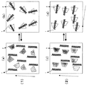
本発明において超分子構造体は、たとえば図1に示すような形態をとる。図1(a)は、環状化合物に鎖状化合物が包接されている状態と解離されている状態である。これら2状態は外部刺激によって可逆的に変化させることができる。ここでは、環状化合物と鎖状化合物は共有結合によって結合しているのではなく、非共有結合による相互作用によって包接錯体をつくっている。図1(a)においては環状化合物が1つ包接されているが、図1(a)’のように複数包接されてもよい。環状化合物と鎖状化合物は、包接−解離を起こす。この挙動を「環状化合物が鎖状化合物上を移動した結果、鎖状化合物上から解離した」と定義する。
【0014】
図1(b)は、図1(a)の超分子構造体の形態において鎖状化合物と環状化合物が修飾基で一体化されている構造体を示す。この形態では一体化されていても図1(a) 同様に包接−解離の可逆挙動を示す。包接体が一体化している場合には、包接−解離の挙動が1分子内で行われることにより効率のよい挙動を示す。また図1(b)’のように鎖状化合物に複数の環状化合物が包接されてもよい。
【0015】
図1(c)は、鎖状化合物が複数個存在し外部刺激によって包接される化合物が変わる超分子構造体を示す。ここでは2種類の鎖状化合物を示したが、これに限らず複数個の鎖状化合物が存在させ外部刺激の程度や形態を複数状態変えることで複数個の包接化合物を形成することもできる。
【0016】
図1(d)は、鎖状化合物が十分に長く環状化合物が鎖状化合物上にあり、外部刺激によって鎖状化合物上を移動する超分子構造体を示す。また、図1(d)’に示すように鎖状化合物は基質分子鎖1に、異なる分子鎖、組成物4、5などの混合体であってもよい。もちろん、混合体の場合、組成物の種類やその数に限定はない。このようないくつかの組成単位の複合鎖である場合には外部刺激によってある特定の部位に止まることもできる。さらに刺激を与えることによって、また異なる部位に固定されることもできる。すなわち、いくつかの異なる組成を持つ分子鎖にすることで外部刺激に応じて任意の部位に環状化合物を配置することができる。ここで、鎖状化合物に包接される環状化合物は1つでも複数個でもよい。
【0017】
以上のような構造をもつ錯体化合物も、超分子構造体に含まれる。本発明においては、鎖状化合物上を環状化合物が移動することができ、広義には解離まですることができる構造体をロタキサン構造と定義する。その挙動は外部刺激によって制御することができる。
これらの超分子構造体は、単独の構造体として用いるばかりではなく、何らかの媒質中(溶媒など)に存在する場合、高分子の架橋構造体(ゲルなど)中に存在する場合、高分子の主鎖中や側鎖として存在する場合、支持バインダー樹脂混合体である場合があり、刺激による分子移動が適宜に行われるような材料系として用いることができる。もちろん上記以外の系も可能であり、その形態を限定するものではない。
【0018】
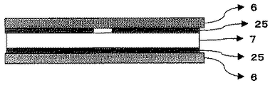
このような超分子構造体材料系は、図2に示すように支持基板と封止材料によって狭持され素子の形態をとる。超分子材料系が高分子フィルムや固体膜の形態を持つ場合には図2(a)に示すように1枚の支持基板6上に超分子構造体を含む系7による膜を形成し、これが外気に直接触れないように封止材料8で封止して素子とすることができる。また、固体でない場合(固体でも可)は図2(b)のように2枚の基板6、9に狭持させて周囲を封止材料10で封止する構成としてもよい。また図2(c)のように、素子内を区画化材料11によって区画化して超分子構造体を含む系7を封入してもよい。このように1枚以上に基板と封止材料によって素子を形成することができる。支持基板は、柔軟性のあるプラスティックフィルムや剛直なガラス材料など超分子構造体を含む系7を支持できるものであればよい。
【0019】
また、素子中は適当な大きさで画素を形成し画素毎に外部刺激を与えられ、光学特性を変化させることによって表示素子となる。画素の大きさは上記の超分子構造体が分子レベルのスイッチング素子であることから、数ナノから数ミリ数センチなど必要な大きさで区切ることができる。
【0020】
また、本素子には支持基板、超分子構造体を含む系7及び封止材料だけではなく、それ以外の機能性膜を挿入することができる。たとえば、超分子構造体の機能を補助、補完するために必要であれば挿入される膜であってもよく、電気の絶縁を実現させる絶縁膜、分子の並び方を制御する配向制御膜、電子や正孔の輸送効率を高めるキャリア輸送層、などが挙げられるがこれに限定するものではない。
【0021】
外部刺激には、電界印加、光(放射線)照射、温度変化(過熱、冷却)などが挙げられる。これらは表示画素ごとに任意の刺激を加えることで任意の表示を行うことができる。これらの外部刺激は単独に用いてもよく、いくつか組合せて用いてもよい。また、これらの外部刺激に限らずここに挙げた以外の外部刺激によって任意の画素に刺激を与えてもよい。
【0022】
超分子構造体の相互作用変化としては、環状化合物と鎖状化合物との包接−解離現象、鎖状化合物上の環状化合物の配置変化とそれによる相互作用状態変化、及びその配置変化による分子形状変化などが挙げられる。このような相互作用変化によって生じる光学特性変化としては、次のようなものがある。
【0023】
一つは、相互作用変化による超分子構造体の配向性、屈折率、分子配列変化によって生じる系の2色性変化、散乱−透過状態変化、光学特性の異方性出現、干渉発色現象である。つぎに、相互作用変化による分子間結合変化、水素結合変化、酸化還元反応、分子内開環・閉環反応、シス−トランス転移、分子内・間水素移動、2量化、イオンの解離・吸着(ドーピング)、ラジカルの解離・吸着(ドーピング)、酸素付加、分子内・間のキャリア移動などに起因する発色、発光現象などが挙げられる。ここで挙げた相互作用や光学変化は一例であり、その種類を限定するものではない。
【0024】
これらの相互作用は、環状化合物と鎖状化合物の分子特性によって生じる。環状化合物は、その形状から内孔(穴)の大きさの違い、内孔部と外孔部の特性の違い、分子左右での特性の違いなどによって相互作用に違いが生じる。一例をあげるとシクロデキストリンは、D−グルコース単位が6、7、8以上の1,4α結合で結ばれて環構造をとる化合物である。シクロデキストリンは、グルコース単位の数で内孔の大きさが決まる。6つのものがα−シクロデキストリン(内径4.5Å)、7つのものがβ−シクロデキストリン(内径6.0Å)、8つのものがγ−シクロデキストリン(内径8.0Å)である。また、内孔が疎水基である反面外孔部(外側部分)は、親水基であるという特徴をもっている。また分子の片側は第2級水酸基を、もう片側には第1級水酸基を有する。これらの特徴から、疎水性の分子で内孔の大きさに合う化合物を内孔に包接することができる。
【0025】
ここではシクロデキストリンの例を参考に説明したが、これに限定するものではなく、環状構造をとることによって包接条件をもつような化合物であればよい。たとえば、シクロファン化合物やクラウンエーテル系化合物、カリックス化合物、DNA等が考えられるし、これ以外の化合物であってもよい。
【0026】
また、上記の環状化合物は、誘導体を有するものでもよい。主として包接相互作用を環状部分に、機能性を誘導体部分に付加させたような環状化合物誘導体を用いることによって外部刺激による機能性を発揮しやすくできる。
【0027】
これに対して、鎖状化合物は基本的には上記のような環状化合物に対して包接される基質から設計する。このような基質に、包接条件の異なる組成部を導入させ外的刺激によって包接条件を変化させれば環状化合物の移動が始まる。または、鎖状化合物、環状化合物が含まれる系の状態を変えることによっても最適な包接状態になるように環状化合物の移動が誘起される。
【0028】
このように、外的刺激によって環状化合物の鎖状化合物上での移動が起こり、相互作用変化につながるのである。つまり、一般的には外部刺激の印加から光学変化に至るまでの過程は、(1)外部刺激の印加、(2)超分子構造体及びそれを含む系の状態変化、(3)分子内もしくは分子の駆動・移動、(4)包接・包接状態の変化、(5)光学変化となる。もちろん系によっては必ずしもこの過程に沿わない場合もあるが、結果的に外的刺激→光学変化が起こればよく、その過程を限定するものではない。
【0029】
このような原理に伴う光学変化は単一分子自身で生じるので、液晶表示素子などのように偏光板を用いる必要も無く明るい表示素子となり得る。また、視野角などの問題も基本的には生じない。また、同じ発色系デバイスであるエレクトロクロミックのような電解質も必要なくデバイスを構築することが可能である。
【0030】
光学変化のスイッチング形態としては、白−黒スイッチング、透明−発色スイッチング、透明−白色スイッチング、発色色相変化、発光などがある。これらを用いた表示素子の形態としては、白−黒スイッチングをもちいた白黒表示素子、さらにカラーフィルターと組み合わせた並列型加法混色によるカラー表示素子、透明−発色スイッチングを用いた発色素子、さらに背面に白色板を用いCMY発色積層による積層型減法混色カラー素子、透明−白色スイッチングと背面吸収板による白黒表示素子、及びさらにカラーフィルターを組み合わせたカラー表示素子、発色色相変化によるカラー表示素子、発光を使ったカラー表示素子などが考えられる。表示素子の形態はこれらに限定されるものではない。
【0031】
以上のような構成によって、新規原理に基づいた新規ディスプレイを提供することができる。
第2の態様
本発明の第2の態様において、上記超分子構造体は上記鎖状化合物が環状化合物を貫通できるロタキサン構造体であり、かつ鎖状化合物の少なくとも1端に前記環状化合物が鎖状化合物から脱離できないような置換基が導入されている超分子構造体であることを特徴とする。
【0032】
上記構成によれば、超分子構造体は前述の超分子構造体図1(d)の構造において少なくとも一端に環状化合物のストッパーとなる置換基を導入した構造になっていてもよい。たとえば、環状化合物がシクロデキストリンの場合には、2−ナフトールアミン6,8−ジスルホン酸モノカリウム塩や2,4−ジニトロフェニル、ダンシル基、トリチル基などを用いることができる。図3(a)に示すように、両端にストッパー12を導入したもの、(b)に示すように鎖状化合物が高分子鎖の側鎖になっており片側がストッパー12であるものなどであってもよい。さらに、(c)のように鎖状化合物は基質分子鎖1にともに異なる分子鎖、組成物4、5などの混合体であってもよい。もちろん、混合体の場合その数に限定はない。さらには、ここでは3種類の超分子構造体をあげたがこれ以外の構造体でもよく、その構造の種類を限定するものではない。
【0033】
鎖状化合物に包接される環状化合物は、1つでも複数でもよい。このように端部をストッパーで止められることによって、環状化合物は区切られた鎖状化合物間を往復運動することになる。(c)のような複数種類の組成の鎖状化合物では外部刺激によって特定の組成部分に環状化合物が停止・配置することができ、その動きは外部刺激によって制御することができる。この場合、鎖状化合物1、環状化合物2に誘導体を導入してもよい。
【0034】
このような超分子構造体を前述したような素子構造として、電界や光(放射線)、熱変化などの外部刺激を与えることで光学特性を変化させ、表示素子とすることができる。
【0035】
超分子構造体の相互作用変化としては、鎖状化合物上の環状化合物の配置変化とそれによる相互作用状態変化、及びその配置変化による分子形状変化などが考えられる。また、ストッパーとして導入する末端基と環状化合物間に生じる相互作用の有無も考えられる。
【0036】
このような相互作用変化によって生じる光学特性変化としては次のようなものがある。一つは、相互作用変化による超分子構造体の配向性、屈折率、分子配列変化によって生じる系の2色性変化、散乱−透過状態変化、光学特性の異方性の出現である。さらには、相互作用変化、相互作用の有無によって生じる、分子間の分子間結合変化、水素結合変化、酸化還元反応、分子内開環・閉環反応、シス−トランス転移、分子内・間の水素移動、2量化、イオンの解離・吸着(ドーピング)、ラジカルの解離・吸着(ドーピング)、酸素付加、分子内・間のキャリア移動などに起因する発色、発光現象などが挙げられる。ここで挙げた相互作用や光学変化は一例であり、その種類を限定するものではない。
【0037】
以上の光学変化を用いて、本発明の第1の態様のようなデバイス構造をとることによって、超分子構造体は表示素子または調光素子とすることができる。
本発明の第2の態様において、超分子構造体は、環状化合物が常に同一の鎖状化合物上をシャトル移動する。上述した本発明の第1の態様における超分子構造体も基本的には同一超分子構造体内の挙動であるが、末端部にストッパーが配置されていないために、基本的には同一超分子構造体内での挙動であるが、環状化合物が外部刺激によって環状化合物は外部刺激によって鎖状化合物から解離することも考えられる。いったん解離してしまうと、再び鎖状化合物に戻らない可能性がある。
【0038】
この現象は、いったん解離した環状化合物や鎖状化合物が系に含まれる他の化合物や不純物と結合したり、鎖状化合物や環状化合物同士で結合あるいは相互作用を起こしてしまうことなどに起因するものと考えられる。このような現象は、超分子構造体の浸食や他の部材の侵食にもつながり、素子の寿命を著しく短くしてしまう。また、いったん解離してしまったものが再度包接する際には、応答速度的も非常に遅くなってしまう可能性もある。また再度包接する際にも、同一鎖状化合物に包接される環状化合物が不均一になることも考えられ、素子の再現性が保たれないおそれがある。
【0039】
本発明の第2の態様において、超分子構造体は、鎖状化合物にストッパーが設けられているので常に同一の鎖状化合物上を、同一の環状化合物が同一個数シャトル移動するために、上記のような問題点を克服した素子とすることができる。
【0040】
以上のような構成によって、特性の再現性、寿命、応答速度に優れた、新規な表示素子または調光素子を提供することができる。
第3の態様
本発明の第3の態様において、表示素子または調光素子は、本発明の第1の態様における上記相互作用変化が、環状化合物と鎖状化合物が包接状態と解離状態をとることを特徴とする。
【0041】
上記態様の構成によれば、超分子構造体が外部刺激によって鎖状化合物と環状化合物の包接、解離現象を誘起し、これに伴う光学特性変化の変化を表示素子に用いる。
【0042】
外部刺激による包接−解離現象は、例を挙げると以下のようして起こりうる。図4では、初期状態では環状化合物2と包接相互作用をつくらない環状化合物1が外部刺激を与えられることによって、分子内に変化を起こし環状化合物の包接条件を満たすような状態となり、包接状態をつくり上げる。また、逆の刺激を与えて包接条件からはずすことで再び解離状態をつくる。このように鎖状化合物を外部刺激で変化させることによって包接−解離を起こすことができる。ここで、外部刺激によって変化を起こさせるのは環状化合物であってもよい。ここでは、鎖状化合物と環状化合物は別々の化合物として示しているが、鎖状化合物が環状化合物の誘導体として形成されているような化合物であってもよい。
【0043】
次に図5では、外部刺激によって鎖状化合物1を変化させ、すでに包接されている鎖状化合物13と入れ替わって環状化合物へ包接される。鎖状化合物が複数存在する場合には、環状化合物との包接相互作用の大きいほうが包接されるので、外部刺激によって鎖状化合物1や交換鎖状化合物13に変化をもたらせ、任意の化合物を包接させることができる。ここでは鎖状化合物は独立な化合物として説明したが、少なくともひとつの鎖状化合物は環状化合物の誘導体として導入してもよい。
【0044】
また図6のように、超分子構造体が含まれる系を変えることで包接−解離を行うこともできる。初期状態では環状化合物に包接されているより超分子構造体を含む系(たとえば、バインダー樹脂中)のほうが安定状態であった鎖状化合物が、外部刺激を与えることで超分子構造体を含む系(たとえば、バインダー樹脂)の状態に変化が起こり、環状化合物中に包接されたほうが安定な状態になれば、環状化合物中に包接されるようになる。逆に、外部刺激によって環状化合物外の超分子構造体を含む系(たとえばバインダー樹脂)のほうが鎖状化合物にとって安定な状態であれば包接化合物から解離される。ここでは、鎖状化合物と環状化合物は別々の化合物として示しているが、鎖状化合物が環状化合物の誘導体として形成されているような化合物であってもよい。
【0045】
同様に図7に示すように、外部刺激によって系の状態を変えることで少なくとも2つ以上の鎖状化合物が存在する場合には、環状化合物中に包接されるほうが安定なものと、系のほうが安定なものとで包接される鎖状化合物を入れ替えることができる。ここでは鎖状化合物は独立な化合物として説明したが、少なくともひとつの鎖状化合物は環状化合物の誘導体として導入してもよい。
【0046】
このように、外部刺激によって環状化合物に対して鎖状化合物を包接させたり解離させたりすることができる。ここでは、4つの例を述べたがその包接−解離の原理はこれに限定されるものではない。
【0047】
また、環状化合物もしくは鎖状化合物が外部刺激、特に電界などと相互作用つまりは静電作用や電荷輸送を起こせる場合には、鎖状化合物の相互作用にかかわりなく鎖状化合物上を移動させることも可能である。すなわち、鎖状化合物上での相互作用を振り切る駆動力として直接外部刺激によって環状化合物を駆動させ、任意の相互作用を引き起こすことができるのである。
【0048】
次にこのような包接−解離が外部刺激によって起こる場合に、どのような光学的変化が生じるかを述べる。
図8では、鎖状化合物、環状化合物及び媒質(バインダー樹脂)からなる超分子構造体の系が包接−解離によって屈折率変調を起こす様子を示している。図8(a)の状態では、鎖状化合物、環状化合物及び媒質(バインダー樹脂)が存在する系であり、それぞれのこの系全体で屈折率が決まる。ここで外部刺激をかけて、包接状態を形成することで系の状態は図8(b)のようになる。ここでは鎖状化合物が環状化合物包接されてしまうので、系の成分に変化が生じ屈折率にも変化を与えることができる。ここでは、1組の包接解離超分子体しか系に示されていないが、いくつかの包接−解離超分子体を系の中に入れていくとこによって、包接時と解離時の成分変化が大きくなり、より大きな屈折率変化を起こすことが可能である。屈折変化が十分に得られれば、包接部分とその他の部分の屈折率差を用いた表示素子、たとえば散乱−透過型変調表示素子や導光板型表示素子のような例が考えられる。
【0049】
図9においては、系の異方性変化について示している。ここで示す系では鎖状化合物と環状化合物のみの系として示しているが、補助的な化合物を混入した系でもよい。また、鎖状化合物は屈折率に異方性を有している。図9(1)の系では、初期状態(a)である程度の一軸性配向状態を鎖状化合物につけて光学的な異方性を持たせておく。ここで、外部刺激によって包接状態をつくらせる(b)と、この配向状態が崩れ系の光学的な異方性が弱くなってしまう。系によっては、異方性が消滅してしまうこともある。また図9(2)の系では初期状態(c)で、ある程度の一軸性配向状態を鎖状化合物につけて光学的な異方性をもたせ、環状化合物もしくは鎖状化合物のどちらかを素子内で固定させておく(ここでは環状化合物を固定した例を示す)。そうすることで、包接状態をつくった状態(d)では、環状化合物に包接された鎖状化合物の配向性が大きく変化し、光学的な異方性の方向が大きく変化する。環状化合物に対して分子長の長い鎖状化合物を用いれば、この光学的異方性の差を顕著にさせることができる。このように、包接−解離の相互作用変化によって、光学的な異方性を変化させることができる。この光学変化の効果を向上させるためには、鎖状化合物と環状化合物の屈折率差がなるべく小さいものがよい。ここでは2つの例を示したが、これに限るものではなくこれ以外の方法でも異方性を持たせてもよい。このように光学的異方性の変化を用いることができれば、光学フィルターや偏向板と組み合わせて光変調表示素子を作成することができる。この系では分子の配列や異方性の方向性などを自由に調整することが可能であるので、液晶表示素子のように2枚以上の光学フィルムを用いることなく効率のよい表示素子を作成することができる。
【0050】
次に図10においては、系の配向性変化特に配向性変化による散乱状態の出現について示している。ここで示す例(1)では、環状化合物、鎖状化合物からなる超分子構造体の系である。ここで、鎖状化合物は、屈折率に異方性を有している。また、鎖状化合物と環状化合物との間に屈折率差をもたせてある。初期状態(a)では、配向性をある程度持たせて素子内に固定化した環状化合物と配向性を持たせない鎖状化合物からなる。この状態では、鎖状化合物の無秩序性と屈折率差から散乱状態となり、白色表示となる。この系に外部刺激を与えて鎖状化合物を環状化合物に包接させると、(b)に示すように、環状化合物が配向性を持つため、包接された超分子体は配向性をもった一つの系となり、透明状態になる。包接される鎖状化合物を複数種類混合すると、初期状態の白色状態は向上する。
【0051】
また(2)の系は、屈曲性鎖状化合物15と環状化合物2からなる系である。初期状態(c)では配向性をある程度もたせて素子内に固定化した環状化合物と無秩序に屈曲した鎖状化合物からなるため、この状態では鎖状化合物の無秩序性と屈折率差から散乱状態となり白色表示となる。この系に外部刺激を与えて鎖状化合物を環状化合物に包接させると、(b)に示すように、環状化合物が配向性をもつため包接された超分子体は配向性をもった一つの系となり、また屈曲性鎖状化合物の分子鎖も伸びて屈折率に異方性ができるために透明状態になる。ここでは2つの例を示したが、これに限るものではなく、これ以外の方法でも散乱状態を発現させてもよい。
【0052】
このように散乱−透過状態を制御することによって、散乱型の表示素子を作成することができる。また、ここでは屈折率の変化も期待できるので前述のような屈折率変化を用いた表示素子を作成することも可能である。
【0053】
また図11に示すように、鎖状化合物がキラル化合物であったり、超分子構造体の系にキラル化合物を混入した場合には、系が螺旋ピッチを持った層構造を形成する場合がある。この場合、この層間隔が可視光の波長領域にあれば、干渉発色を起こす(図11(a))。この状態において、外部刺激によって包接状態を制御すれば、各層の分子構成に変化がもたらされるので層間隔が変化し、構造発色の色調を変化させることができる(図11(b))。さらには、包接体を作成することによって層構造を解消し、散乱状態にすることもできる(図11(c))。
【0054】
このように散乱−透過状態を制御することによって、散乱型の表示素子を作成することができる。
次に図12を用いて化合物間の相互作用による発色・発光現象について述べる。鎖状化合物及び環状化合物からなる系では、外部刺激によって解離状態(図12(a))と包接状態(図12(b))を形成するが、解離した状態では互いの化合物は相互作用をもたない化合物単体の状態であり、包接した状態では鎖状化合物の組成基と環状化合物の組成基が相互作用を起こしている状態をつくっている。また、超分子構造体の系に鎖状化合物と相互作用を起こすような顕色化合物16を混入した場合には、包接と解離によって鎖状化合物が環状化合物と相互作用を起こしている状態(図12(b))と、顕色化合物16と相互作用を起こしている状態(図12(c))がある。
【0055】
このように、分子同士が相互作用を起こしている場合には、分子間の分子間結合変化、水素結合変化、酸化還元反応、分子内開環・閉環反応、シス−トランス転移、分子間水素移動、2量化、イオンの解離・吸着(ドーピング)、ラジカルの解離・吸着(ドーピング)、酸素付加、分子間のキャリア移動、分子内キャリア移動などに起因する発色、色相変化、発光が起こることがある。発光や発色は相互作用の種類や強さなどによってさまざまな形態をとるし、分子構造の設計によって発色や発光の色調を調整することもできる。有機化合物ではこのような色調の変化を制御しやすい利点がある。このような分子間の相互作用による発色を用いることができれば発色型表示素子が、発光を用いることで自発光素子を作ることができる。これらの素子は基本的に分子の包接解離によって発現する現象であり、ECDのような電解質は必要なく発色させることができるし、有機ELのようには大量の電流量を流さなくても発光させることも可能である。
【0056】
図13を用いて、発光、発色のもう一つの形態について述べる。ここでは、鎖状化合物、環状化合物、バインダー樹脂からなる超分子系において発現する。鎖状化合物の中には同一分子同士で相互作用を起こすものや、複数の鎖状化合物を系に混入した場合には鎖状化合物同士で相互作用を起こすものがある。このような鎖状化合物に対して、解離状態では相互作用を阻害するようなバインダー樹脂を用いることによって、相互作用を阻害する。ここで外部刺激を与え、包接状態になり鎖状化合物が相互作用阻害バインダーから隔離され、環状化合物内を一種の反応場として用いることで鎖状化合物が相互作用を起こし発色・発光を起こすことができるようになる。
【0057】
反応場としての包接状態は、(a)に示すように2つの環状化合物と2つの鎖状化合物が包接されている場合や、一つの環状化合物内に複数の鎖状化合物を包接する場合などが考えられるがこの限りではない。
【0058】
相互作用によって、分子間の分子間結合変化、水素結合変化、酸化還元反応、分子内開環・閉環反応、シス−トランス転移、分子間水素移動、2量化、イオンの解離・吸着(ドーピング)、ラジカルの解離・吸着(ドーピング)、酸素付加、分子間のキャリア移動、分子内キャリア移動などが起こることで発色、発光が起こる。このような分子間の相互作用による発色を用いることができれば発色型表示素子が、発光を用いることで自発光素子を作ることができる。発色・発光の形態等は前述のものと同様である。
【0059】
以上のように、包接−解離の相互作用によって、さまざまな光学的変化が生じ新規原理に基づく表示素子を提供することができる。本発明の第4の態様において、表示素子または調光素子は、本発明の第1から第3の態様における相互作用変化が、環状化合物の鎖状化合物上における停止位置変化であることを特徴とする。
【0060】
上記構成によれば、超分子構造体中の環状化合物が外部刺激によって、鎖状化合物上を移動し、これに伴う光学特性変化の変化を表示素子に用いる。
第4の態様
前述の本発明の第3の態様においては、環状化合物と鎖状化合物の相互作用によって包接状態と解離状態の2つの状態変化を説明した。本発明の第4の態様においては、鎖状化合物上に環状化合物と複数の相互作用を起こす組成が鎖状化合物に形成され、外部変化によって相互作用を起こす位置が変化しその変化に伴って光学変化を引き起こすものである。そのため、外部刺激によって環状化合物は鎖状化合物上を移動することができるが、本発明の第2の態様のように解離する必要はない。
【0061】
外部刺激による環状化合物の鎖状化合物上の位置変化は、例を挙げると以下のようにして起こる。基本的な相互作用の起こり方、変化については前述の本発明の第3の態様において挙げた例と同様である。
【0062】
図14によれば、鎖状化合物1には環状化合物2と包接相互作用をとる組成部分4、5が複数含まれていて、外部刺激に相互作用の程度に変化を生じさせ、より相互作用しやすい部位に環状化合物が移動する。また図15によれば、超分子構造体を含む系が外部刺激によって状態変化を起こし、それに伴って環状化合物と鎖状化合物との相互作用の起こしやすさに変化が生じ、環状化合物の位置変化を起こす。図16に示すように、鎖状化合物が超分子構造体外部の化合物と相互作用を起こしている場合、外部刺激によってその相互作用に変化をもたらせて環状化合物の位置変化を起こさせることができる。さらに図17のように、環状化合物2が誘導体基3をもちその誘導体基3と鎖状化合物1上の組成部分4、5の相互作用の相互作用によって決まる環状化合物2の停止位置を外部刺激によって、上記相互作用の状態に変化をもたらせ停止位置を変えさせることができる。
【0063】
このように外部刺激によって相互作用の状態変化を生じさせ、環状化合物の停止位置を変えることができる。ここでは、4つの例を示したが停止位置を変える原理、方法はこれに限るものではなく可逆的に環状化合物の停止位置を変えるのであればよい。
【0064】
ここでは、環状化合物の停止位置として、鎖状化合物上に2つ以上の相互作用を起こしうる組成部位が必要である。これらは異なるものでもよいし、同じものでもよい。同じ組成部位でも環状化合物からの距離や誘導基などによって位置を変える可能性がある。また、複数種類の相互作用を起こす組成部位を導入し、外部刺激によってある組成部では停止、ある部位では通過など停止位置を自由に変えることも可能である。もちろん1本の鎖状化合物内に取り込まれる環状化合物も複数あってもよく、外部刺激によって停止できるものとできないものを制御することも可能である。
【0065】
また、環状化合物が外部刺激、特に電界などと相互作用つまりは静電作用や電荷輸送を起こせる場合には、鎖状化合物の相互作用にかかわりなく鎖状化合物上を移動させることも可能である。前述の本発明の第4の態様における鎖状化合物上での相互作用を振り切る駆動力として直接外部刺激によって環状化合物を駆動させ任意の相互作用を引き起こすことができる。
【0066】
このような、環状化合物の停止位置変化によって生じる光学変化について説明する。前述した本発明の第3の態様のように環状化合物は鎖状化合物上で相互作用を形成している。また、系の内外の他の化合物と相互作用を形成しているものもある。このような場合には、これらの状態が環状化合物の移動及び停止位置の移動によって変化すれば、分子間の分子間結合変化、水素結合変化、酸化還元反応、分子内開環・閉環反応、シス−トランス転移、分子間水素移動、2量化、イオンの解離・吸着(ドーピング)、ラジカルの解離・吸着(ドーピング)、酸素付加、分子間キャリア移動、分子内キャリア移動などに起因する発色、発光が起こることがある。発光や発色は相互作用の種類や強さなどによってさまざまな形態をとるし、分子構造の設計によって発色や発光の色調を調整することもできる。
【0067】
このような分子間の相互作用による発色を用いることができれば発色型表示素子が、発光を用いることで自発光素子を作ることができる。これらの素子は基本的に分子の相互作用変化によって発現する現象であり、ECDのような電解質は必要なく発色させることができるし、有機ELのようには大量に電流量を流さなくても発光させることも可能である。
【0068】
また、これらの光学変化は前述の本発明の第3の態様のように、超分子構造体の包接−解離現象によって起こるのではなく、1本の鎖状化合物上での移動によって起こるので、応答速度も速くなる。また、基本的に分子内での相互作用なので、解離した環状化合物や鎖状化合物が系に含まれる他の化合物や不純物と結合したり、鎖状化合物や環状化合物同士で結合あるいは相互作用を起こしてしまうことがなく、素子の再現性や安定性もよい。さらには、鎖状化合物上に複数の環状化合物が包接され、外部刺激による移動を制御し、鎖状化合物上での凝集、分散によっても上記のような相互作用、ひいては光学変化を起こすことができる。
【0069】
また、環状化合物の鎖状化合物上での移動は、分子の特性を変化させることができる。鎖状化合物上の複数個の環状化合物を鎖状化合物に均一に配置した場合と、末端部あるいは中心部に凝集した場合では分子の特性が異なる。たとえば、中心に凝集させた場合には、鎖状化合物は構造的に液晶化合物と類似したものになり、液晶性を有するようになる。液晶性を有することができれば分子配列が起こり、その配列状態によって光学的性質が変わる。ネマティック配列や、スメクティック配列のような分子配向秩序を持てば偏向板との組み合わせによって光の透過率をコントロールすることができる。また、コレステリック配列を取れば各層の層間隔によって干渉色発色を起こすことができる。
【0070】
これ以外にも、分子の末端部に環状化合物を凝集させても超分子構造体の分子配列に大きな影響を与え、上記のような光学変化を起こすことが可能である。分子設計によっては、環状化合物の位置によって他の分子や超分子構造体同士との相互作用に変化を与え、系全体での相互作用つまりは、分子間結合変化、水素結合変化、酸化還元反応、分子内開環・閉環反応、シス−トランス転移、水素移動、2量化、イオンの解離・吸着(ドーピング)、ラジカルの解離・吸着(ドーピング)、酸素付加、キャリア移動などに起因する発色、発光を起こすことも可能である。
【0071】
また、環状化合物の鎖状化合物上の位置変化によって鎖状化合物の立体配置や相互作用変化、環状化合物の均一な配置と特定部分への凝集によって上記のような環状化合物の鎖状化合物の形状変化を起こすこともできる。直線状の鎖状化合物が、外部刺激によって相互作用変化を起こし屈曲系に変化した場合にも上述したような配向秩序の変化等によって光学的変化を引き出すことができる。
【0072】
こうして得られる光学変化を用いて、前述の本発明の第1の態様のようなデバイス構造をとることによって、超分子構造体は表示素子または調光素子とすることができる。
【0073】
以上のような、超分子構造体の環状化合物の位置変化による光学変化を用いることによって新規原理に基づく表示素子を提供することができる。
第5の態様
本発明の第5の態様において、表示素子または調光素子は、本発明の第2の態様の構成において上記相互作用変化が末端部と環状化合物との相互作用による鎖状化合物上移動であることを特徴としている。
【0074】
上記構成によれば、鎖状化合物はストッパーとしての末端基を少なくとも片方に備え、末端部と環状化合物の相互作用によって環状化合物が鎖状化合物上を移動させ、それによって生じる光学特性変化を表示素子として用いる構成である。
【0075】
前述の本発明の第3及び第4の態様においては、鎖状化合物上の特定部位と環状化合物との相互作用によって光学変化を引き起こした。ここでは、鎖状化合物の末端部に相互作用を引き起こさせ、外部刺激によってその相互作用を引き離させることによって相互作用変化とし、これによって生じる光学変化を表示素子として用いる。ところで、環状化合物の移動速度は鎖状化合物上に相互作用を引き出させるような部位がないほうが高速である。前述の相互作用は、環状化合物の移動にとって鎖状化合物との相互作用は、ある場合には障害物となりうる部位間を移動することになる。そうすれば外部刺激に対する応答速度は低くなる可能性がある。これに比べて末端部分での相互作用で鎖状化合物上は移動のみに用いれば分子内での高速応答を十分に発揮することができる。
【0076】
末端部分による環状化合物の移動については以下のような例が挙げられる。
図18では、末端基12に誘導された誘導組成部18と環状化合物の誘導体3が非共有結合によって包接相互作用状態にある。これを外部刺激によって切り離し相互作用状態を変化させる。切り離れた環状化合物は反対側の末端基まで移動してもよいし、途中で止まってもよい。反対側に環状化合物の誘導体部分と相互作用を引き起こす組成を形成すれば反対側の末端部にも固定配置することができる。いったん切り離された環状化合物に再び外部刺激を加えることによってもとの場所に戻すこともできる。環状化合物と末端部では静電気力、分子間力、水素結合、イオンの授受、キャリアの授受等によって相互作用を形成し、これらの相互作用によって前述の本発明の第3及び第4同様の、発色や発光現象を引き起こさせることができる。同様に、図19のように、末端部及び組成部分19と環状化合物そのものが包接相互作用を起こしている状態であり、外部刺激によって包接相互作用状態を切り離す系、図20のように、環状化合物そのものと誘導体がどちらも包接相互作用を有してこれを外部刺激によって切り離す系などが考えられる。これらは、鎖状化合物の末端部のうち、図18から20に示すように、片方のみに導入してもよいし、図21のように、両側に導入してもよい。両側に導入する場合には、両端の包接相互作用は同じものでもよいし、異なるものでもいい。また、鎖状化合物がポリマー状でいくつもの分岐状態を形成している場合には、それぞれの末端基に上記の包接相互作用の系を自由に組み合わせることも可能である。さらに図21に示すように、鎖状化合物上に前述の本発明の第3の態様で示したような環状化合物の停止位置となる組成部を組み込んでもよい。また、鎖状化合物上には1つの環状化合物が導入されている例を述べたが、これに限らず図22に示すように、鎖状化合物の両端に相互作用を引き起こす環状化合物が導入され、外部刺激によって、環状化合物同士が接近、相互作用を引き起こすようにすることもできる。
【0077】
また、環状化合物が外部刺激、特に電界などと相互作用つまりは静電作用や電荷輸送を起こせる場合には、鎖状化合物の相互作用にかかわりなく鎖状化合物上を移動させることも可能である。前述の本発明の第4の態様における鎖状化合物上での相互作用を振り切る駆動力として直接外部刺激によって環状化合物を駆動させ任意の相互作用を引き起こすことができる。
【0078】
このように相互作用を形成している状態と、外部刺激によって切り離された状態との光学特性の変化によって表示素子とすることができる。この系では、鎖状化合物の末端部に片方のみ相互作用を引き起こす組成部を導入することによって、相互作用の有無によるスイッチングを行うことができる。両側の末端部に同じ相互作用を引き起こす組成を導入しても切り離された状態が維持できれば相互作用の有無によるスイッチングを行うことができる。両側の末端部に異なる相互作用を引き起こす組成を導入すれば、多色発色及び発光、発色と発光などを組み合わせた多機能表示が可能なスイッチングを行うこともできる。また、鎖状化合物上に環状化合物の停止位置となる組成部を組み込めば、両側の相互作用状態を制御するストッパーになるばかりか、末端部と鎖状化合物上の相互作用を組み合わせたさらに多機能化が可能になるスイッチング素子を作成することができる。
【0079】
また、図23に示すように、環状化合物に誘導基3に輸送基20を導入し外部刺激によって環状化合物もしくは誘導体との包接相互作用を切り離し、輸送基20に輸送体21を付与させて反対側の末端基部分へ輸送体を運ぶ系によっても相互作用変化を起こさせることができる。輸送体としてはキャリア及びイオン体などが考えられるが、これらに限定されるのもではない。これらの輸送体を末端基から引き離したり、輸送体が付着したりすることで末端基部分の状態変化が起こり光学変化を発現させることができる。
【0080】
以上のような、環状化合物の移動によって起こる光学変化は前述したように、末端部分との環状化合物の相互作用における、静電気力、分子間力、水素結合、イオンの授受、キャリアの授受等による、本発明の第3及び第4の態様と同様の、発色や発光現象が考えられる。さらに、図24に示すように、キャリア輸送による光学変化も起こる。たとえば、外部刺激によって発現させたキャリアを輸送基に付与させ(図24(a)、(b))、反対側には対になるキャリアを発現させ(図24(a))、さらに外部刺激によって反対側の末端基まで環状化合物を移動させ、キャリアと対キャリアを結合させる(図24(c))。これによって、発光もしくは発色現象を引き起こすことができる。同様に、イオン対の移動によってイオンドーピングによって吸収波長が変化するような化合物を末端基部分に導入することでイオンドープ−脱ドープによる発色型スイッチングを行うことができる。
【0081】
図25,26に示すように、擬似発色団の形成による発色を起こすこともできる。発色を示す化合物は基質となる発色団を有することがある。たとえば図26に示すように、インジコなどの色素を形成するH型発色団などがその例である。このH型の発色団を図26(a)に示すように、環状化合物の誘導基と末端部の化合物誘導基に分割するような形で形成し、図26(b)のような環状化合物の移動によって末端基部に環状化合物が配置された際に分割された発色団が擬似的に発色団を形成し、発色現象を起こさせる。これはこのタイプの発色団に限らず、適応できる発色団を形成すればよい。
【0082】
このように、末端基からの環状化合物移動によってさまざまな光学変化を引き起こすことができる。この系では、鎖状化合物の末端部分がストッパーとして働くため環状化合物が鎖状化合物から飛び出すことがない。そのため、再現性のよい素子にすることができる。また、鎖状化合物上は主に環状化合物の移動に使われるので、スイッチングスピードが速く動画表示にも対応できる。また、素子のスイッチングはキャリア移動も含めて単一の超分子構造体で行われるので、他分子と相互作用してしまったり、過剰な反応や不均一な反応が起こらず均一で信頼性の高い素子とすることができる。
【0083】
このように、末端部と環状化合物の相互作用によって環状化合物が鎖状化合物上を移動させ、それによって生じる光学特性変化を用いることによって新規原理に基づく表示素子及び高速応答速度、高い信頼性も有する表示素子を提供することができる。
第6の態様
本発明の第6の態様において、表示素子または調光素子は、本発明の第1から第5の態様の構成において上記支持基板が電極を備え、電気的刺激によって上記超分子構造体の相互作用を制御することを特徴としている。
【0084】
上記構成によれば、電気信号によって超分子構造体の光学変化を制御し表示素子とする。表示領域を電極によって分割することで、任意の画素に電界を印加し任意の表示を行うことができる。また、電界印加によって表示の書き換え、さらには動画表示を任意に行うことができる。
【0085】
また、環状化合物が静電特性などを有している場合には、鎖状化合物との相互作用にかかわりなく電界の極性によって鎖状化合物上を移動させることも可能である。前述の本発明の第3及び第4の態様のように環状化合物と鎖状化合物の相互作用をもたせた系であっても、その相互作用にかかわりなく電界のみで鎖状化合物上を移動させることも可能である。この場合は、電界強度による環状化合物の移動駆動力と、環状化合物と鎖状化合物の相互作用の比較によって環状化合物の移動条件も変わり、またそれを制御することによって光学変化を発現させ制御することも可能である。
【0086】
また、環状化合物と鎖状化合物との相互作用で発生した静電気や電荷などをフレッシュアップすることも可能である。
このように電気信号による制御によって書き換え可能,さらには動画表示も可能な表示素子および、環状化合物を可動させる駆動力となる表示素子を提供することができる。
第7の態様
本発明の第7の態様において、表示素子または調光素子は、本発明の第6の態様の構成において上記電気的刺激を上記支持基板の上下から与えることを特徴としている。
【0087】
上記構成によれば図27に示すように、超分子構造体の上下に電極を設け、電界印加を行うことによって表示を行う。電極を上下方向に形成することによって、表示領域で分割された画素に均一に電界を印加することができる。上記超分子構造体のスイッチングにおいては、化合物やキャリアのやりとりを行う場合も多く、それらのやりとりを同一画素中で行うことが素子の均一性に非常に重要である。そのためには、画素に対して垂直方向つまり超分子体に対して上下から電界を印加させるとよい。上下からの電界駆動としては、それぞれストライプ上に切った電極を上下で垂直に重ねるパッシブ電界駆動、少なくとも片方基板にアクティブ素子を設けたアクティブ駆動などの電界印加法が考えられるが、これらに限らず上下から電界をかけられる方式であればよい。
【0088】
このように超分子体に上下から電界を印加することによって、書き換え可能,さらには動画表示も可能な表示素子を提供することができる。
第8の態様
本発明の第8の態様において、表示素子または調光素子は、本発明の第6の態様の構成において上記電気的刺激を上記支持基板に対して同一平面上から与えることを特徴としている。
【0089】
上記構成によれば、図28に示すように、電極を同一平面上から印加させるインプレイン型電界印加法によって表示素子を形成する。超分子構造体による素子を形成する場合、1枚基板上に電極や超分子材料などの部材を積層して素子を形成する方法、2枚の基板に電極を形成し部材を積層した後両基板を貼り合わせる方法などが考えられる。1枚基板上へ積層する方法で、上下に電極を設ける場合には,超分子構造体あるいは有機材料上に電極パターンを形成する工程が入る。有機材料上の電極材料の工程は紫外線照射、アルカリ、酸による処理など有機材料を侵食する工程が有り、超分子構造体及び有機材料の材料特性に悪影響を与えてしまうおそれがある。
【0090】
一方、2枚基板を重ね合わせる方法では、基板が2枚必要で素子の厚みを2倍にしてしまうし、貼り合わせ面での接合面の界面密着性が積層より弱くなって素子の機能性を低下させるおそれがある。これらの問題点を解決するためには、基板上に横電界をかけられるように電極を形成し、その上に有機樹脂を順次積層して素子を作成すれば、有機樹脂上に電極工程を行う必要なく、各部材の接合界面の密着性も損なうことない素子を作成することができる。平面電極の形状としては図29に示すように、同一基板上に形成される(図29(a))、保護層を介して形成(図29(b))、対抗電極を形成後、保護層のスルーホールを通じて平面状に電極を形成(図29(c))、などの方式が考えられるがこれに限定させるものではない。超分子構造体の上下どちらか片方のみに電極が形成されるような構造であればよい。平面上の電極形成においても、パッシブマトリックス状電極、アクティブ素子によるアクティブマトリックスなど素子の性能に応じた電極を形成することができる。
【0091】
このように、平面上に電極を形成することによって、有機材料に悪影響を及ぼすことなく素子が作成され、書き換え可能,さらには動画表示も可能な表示素子を提供することができる。
第9の態様
本発明の第9の態様において、表示素子または調光素子は、本発明の第1から第6の態様の構成において上記超分子構造体が上記基板に対して垂直もしくは略垂直または平行もしくは略平行に配向していることを特徴している。
【0092】
上記構成によれば、超分子構造体が配向性を有する素子である。機能性材料をデバイスとして機能させるには、分子同士が機能性を打ち消さないようにする必要がある。特に外部刺激を与える方向に対してどのような方向にあるかが重要である。外部刺激の方向に対して分子の向きや、配向方向が各分子同士で異なっている場合には、外部刺激に対して機能性が発現したりしなかったり、逆方向の機能性によって機能性を消失させたりなど、外部刺激を与えた単位領域内で機能性を効果的に発揮することができない。そのため、超分子構造体は一定の配向性さらには、一定の方向性を持つことが必要である。特に外部刺激は超分子構造体に対して垂直方向や横方向に与えられるので、この方向に配向することが機能を効果的に出すために必要である。
【0093】
超分子構造体の配向性については、液晶分子で見られるようなネマティック相配列やスメクティック相配列が考えられる。隣接分子の影響を受けないようにするためには、スメクティック層のような配列の方がより望ましいであろう。
【0094】
配向性を持たせるためには、超分子構造体を含む系に配向性を持つ分子を混合させたり、超分子構造体を高分子化したり、配向性を有する組成を導入したり、超分子構造体自体に配向性の機能を有するものとしてもよい。また、超分子構造体を配向制御層上に配列させてもよい。さらには、超分子自身の包接現象などの機能によって一定の分子配列を行うこともできる。
【0095】
このように、配向性及び分子の配列に秩序を持たせれば、外部刺激に対して、超分子構造体の機能が十分発揮でき表示素子として機能することができる。
このように、超分子構造体を配向させることによって機能性を効果的に発現させることができる。
第10の態様
本発明の第10の態様において、表示素子または調光素子は、本発明の第1から第9の態様の構成において上記超分子構造体が単一分子内で相互作用変化および光学変化を完結することを特徴としている。
【0096】
上記構成によれば、超分子構造体の相互作用が単一分子内で完結する。超分子構造体は外部刺激によって相互作用が変化し光学変化を誘起するが、超分子構造体が近接している場合には同一分子内での相互作用だけでなく、近接超分子構造間での相互作用が起こってしまう可能性がある。一分子内での相互作用では、分子内のやりとりが完結するが、他分子同士のやりとりが行われると、相互作用を起こす箇所、起こさない箇所、過剰に起こす箇所など相互作用が系内で不均一に成る。このため、単分子で起こる光学変化が発現されなかったり、効果が小さくなる。
【0097】
また、素子としては外部刺激によって光学変化が可逆的に発現することが素子として必要であるが、上記のような超分子構造間での相互作用は必ずしも可逆性をもたない相互作用を形成することも考えられ、外部刺激による制御が不可能になる。また、不均一な相互作用は不可逆な残留化合物となり系の不純物や他の樹脂膜を侵食し素子の破壊につながることも考えられる。
【0098】
このような課題を解決するには、単一分子内で相互作用を完結させることが必要である。そのためには、分子間の距離を保つように配列させればよい。超分子構造体の分子内での相互作用の方が分子間の相互作用より強い範囲外に分子を配置すれば単一分子内で相互作用が完結する。さらには、この位置で分子を固定させておけばさらに分子内相互作用の完結性が向上する。
【0099】
このように、分子間の配置を規定する方法は、配列を制御する膜を使用したり、ポリマー鎖によって配列を規定する方法などが考えられ、超分子構造体を含む系に配向性を持つ分子を混合させたり、超分子構造体を高分子化したり、配向性を有する組成を導入したり、超分子構造体自体に配向性の機能を有するものとしてもよい。また、超分子構造体を配向制御層上に配列させてもよい。さらには、超分子自身の包接現象などの機能によって一定の分子配列を行うこともできる。
【0100】
このように分子の配列を単分子内で相互作用が完結する範囲に規定することで、信頼性に優れ、機能性を発揮できる素子を提供することができる。
第11の態様
本発明の第11の態様において、表示素子または調光素子は、本発明の第1から第10の態様の構成において上記素子が支持基板または支持基板に備えた電極と超分子構造体間に、少なくとも一層以上の中間層含むことを特徴としている。
【0101】
上記構成によれば、素子内特に超分子構造体の上下に機能性膜を形成する。これらの機能性膜は、外部刺激の効果を向上させるような機能を持ったものや、配向秩序を制御させる効果のあるもの、キャリア、イオンの注入などが挙げられる。これらの膜を超分子構造体の少なくとも片側に形成することによって、前述の本発明の態様で説明した超分子構造体の相互作用や、分子の配向性、分子間相互作用を防ぐような配列を効率よく行うことができる。また、超分子構造体の機能を向上させることもできる。
【0102】
このような機能性膜は、1層のとどまらず必要に応じて何層も積層させたり、外部刺激の最小単位内で異なる機能性膜を形成したり、超分子構造体の上下で異なる機能性膜を異なる構成で形成してもよい。
【0103】
このように、機能性膜を用いることで光学変化を効率よく行い、また再現性や均一性に優れた表示素子を提供することができる。
第12の態様
本発明の第12の態様において、表示素子または調光素子は、本発明の第11の態様の構成において上記中間層が電極と超分子構造体間に設置され、電界印加時の電極を備えた支持基板と超分子構造体間のインターフェイスとして機能することを特徴としている。
【0104】
上記構成によれば、電極と超分子構造体間に機能性膜を形成し、電界印加の効果を超分子構造体に効果的に伝達させる。
前述したように、外部刺激に対して超分子構造体の相互作用ひいては光学特性変化を効率よく発現させるためには、超分子構造体を一定の秩序を持たせて配向させることが必要である。それに加えて、外部刺激が電気刺激つまり電界印加の場合には、電界の効果を超分子構造体に効果的に伝達する必要がある。特に、電荷の注入放出を伴う相互作用系の場合には電極と直接的に超分子構造体を接合させることが必要である。もちろん、電荷の極性と超分子構造体の電荷伝達の方向が一致していなければ機能性を発現させることはできない。
【0105】
そこで、電極と超分子構造体間にインターフェイス材料を形成することによって電界の効果を高めることができる。この場合、この機能膜は電極及び超分子構造体どちらにも表面の相互作用をもち、お互いを結びつけ、さらに超分子構造体の配向性を制御させることができる。さらに、前記機能膜が電荷輸送能力を持たせることができれば電極−超分子構造体間のインターフェイスとして機能させることができる。
【0106】
このように、電極−超分子構造体間にインターフェイス機能膜を形成することによって電界印加の効果を高め超分子構造体の機能を効率よく発現させることができる。
第13の態様
本発明の第13の態様において、表示素子または調光素子は、本発明の第1から第6の態様の構成において上記超分子構造体又は前記超分子構造体を含む系が固体であることを特徴としている。
【0107】
上記構成によれば、素子が全固体型である。超分子構造体が液体もしくは流動性を有する場合には液漏れや液による基板部材の侵食などの悪影響を引き起こす可能性がある。また、液状の超分子構造体は上下2枚基板間に封入する素子構造になるが、その際充分な脱気を行わなければ温度変化や大気圧変化によって素子中に気泡が生じてしまう。また、脱気する際には超分子構造体の成分が蒸発し成分の組成変化が起こる可能性もある。
【0108】
これに対して、固体の素子にすることで、このような課題を回避することができる。また、固体であれば積層プロセスが可能で1枚基板での素子作成も可能となる。素子の固体化する方法には、超分子構造体自身がフィルム化できるような分子設計にする方法、ポリマー化することによってフィルム化する方法、超分子構造体に包接架橋させることによってゲル化、固体化する方法、および超分子構造体をバインダー樹脂中に混入しフィルム化する方法などの方法が考えられるが、これに限定することなく超分子構造体の系が固体化されればよい。
【0109】
また、超分子構造体では鎖状化合物部分がポリマー化されても外部刺激による分子スイッチは単位分子内での環状化合物の移動によって行われるので、高分子化や固形化によって素子の応答速度に対する影響が小さくて済む。このことは、高分子化によって素子の応答が著しく劣化することに比べて非常に優れた特徴である。
【0110】
このように、全固体型素子にすることで信頼性の高い素子を提供することができる。
第14の態様
本発明の第14の態様において、表示素子または調光素子は、本発明の第1から第13の態様の構成において上記超分子体の環状化合物が複数の環状化合物で形成されたチューブ状化合物であることを特徴としている。
【0111】
上記構成によれば、環状化合物が複数の環状化合物が接合されることからなるチューブ状化合物からなっている。表示素子を外部刺激で制御するためには外部刺激に対して光学変化を起こす閾値を有することが望まれる。特に有機化合物の相互作用変化では微小な状態変化や外部条件の変化(温度、気圧、紫外線)によって相互作用変化が進むことが多い。そのため、外部刺激を与えた後も光学変化が持続したり、不必要なときにも光学変化が起こることがある。これでは、素子を外部刺激によって制御することができなくなり、表示素子として機能しない。
【0112】
この課題に対して、超分子構造体に閾値を持たせることで、一定の刺激以下では変化しないようにさせることが必要である。つまりは、超分子構造体中に相互作用を起こしにくい要因を形成すればよい。ここでは、環状化合物をいくつも接合したチューブ状にすることによって、相互作用効果を強くして外部刺激による相互作用変化を起こしにくくすれば、一定の閾値を持たせることができる。チューブの長さや形成法は必要な閾値や鎖状化合物の長さに合わせればよい。
【0113】
このように、チューブ状環状化合物を用いることによって素子に閾値を与え、信頼性の高い表示素子を提供することができる。
第15の態様
本発明の第15の態様において、表示素子または調光素子は、本発明の第1から第14の態様の構成において上記超分子構造体の環状化合物が鎖状化合物中に複数個包接されていることを特徴としている。
【0114】
上記構成によれば、環状化合物が鎖状化合物状に複数包接されていて、環状化合物同士が鎖状化合物上で相互作用を起こしている。上記本発明の第14の態様で説明したように素子を外部刺激で制御するためには超分子構造体に閾値を持たすことが必要である。ここでは、鎖状化合物上に複数の環状化合物を包接させることによって、環状化合物同士が相互作用を起こし、環状化合物の移動が起こりにくくすることで一定の閾値を持たせることができる。鎖状化合物に包接させる環状化合物は同じ化合物を用いてもよいし、異なる化合物を用いてもよい。包接させる個数も必要な閾値や鎖状化合物の長さによって調整すればよい。
【0115】
さらに本構成の効果として、複数個の環状化合物の鎖状化合物上での凝集・分散によって相互作用の変化をもたらし光学特性や超分子構造体の物性に変化をもたらせることができる。環状化合物の凝集によって液晶性を持つ例が報告されていることなどもあり、このような分子形状の変化によって超分子体の配向性を高めることも可能であり、超分子の機能性を高めることになる。
【0116】
このように、環状化合物を複数個包接することによって素子に閾値を与えたり、超分子構造体に新規な機能性を付加することができ、信頼性の高い表示素子を提供することができる。
第16の態様
本発明の第16の態様において、表示素子または調光素子は、本発明の第1から第6の態様において上記環状化合物がチューブ状であり、鎖状化合物がチューブ内を移動することを特徴としている。
【0117】
上記構成によれば、チューブ状の環状化合物内を鎖状化合物が移動しその相互作用変化によって光学変化を起こし表示素子とする。
図30に示すようにチューブ状の環状化合物内を外部刺激によって、鎖状化合物が移動する。図31に示すように環状化合物内に相互作用を起こすような組成部があれば、本発明の第3、第4の態様のような相互作用による光学変化を引き起こすことができる。また、末端基に鎖状化合物と相互作用を引き起こす誘導体をつけることによって、本発明の第5の態様のような末端基間のスイッチングを引き起こすことも可能である。さらに、鎖状化合物自身もしくは誘導体に輸送基をつけることで、本発明の第5の態様に示すような電荷やイオンなどの輸送型素子を作ることもできる。
【0118】
このようにチューブ状化合物内を鎖状化合物が移動することによっても相互作用変化を生じさせ、光学変化を引き起こした表示素子を作ることができる。
ここで、チューブ状化合物は、環状化合物がポリマー化したものでもよいし、DNAなどの鎖状分子による螺旋構造体でもよい。
【0119】
この系では、鎖状化合物は環状化合物内で移動するため、環状化合物外部の影響を受けずにスイッチングでき、信頼性の高い素子を作成することができる。
このように、チューブ状化合物内で鎖状化合物を動かす系によって新規原理に基づいた表示素子、特に信頼性の高い表示素子を提供することができる。
第17の態様
本発明の第17の態様において、表示素子または調光素子は、本発明の第1から第6の態様において上記超分子構造体は外部刺激を与えられる最小単位内に少なくとも2種類以上の異なる構成単位を持つことを特徴としている。
【0120】
上記構成によれば、1画素内で外部刺激の違いによって超分子構造体の応答が異なり、階調表示を可能にする。表示素子としては、外部刺激に対する閾値が明確であると同時に、同一画素内で異なる刺激に追随して表示状態が変化できる階調表示ができることが望ましい。
【0121】
外部刺激に対する安定状態が2つある場合には、外部刺激の変化を調整することで状態変化ひいては光学変化を任意に調整することができない。そこで、閾値の異なる構造体を複数種類混入することで画素内において閾値変化が生じ外部刺激の変化に応じた表示状態の変化をもたらし、階調表示を可能にすることができる。
【0122】
このように、1画素内に異なる閾値を持つ超分子構造体を配することで階調表示が可能な表示素子を提供することができる。
第18の態様
本発明の第18の態様において、表示素子または調光素子は、本発明の第1から第17の構成において上記構造体を構成する系に、少なくとも2種類以上の鎖長の異なる鎖状化合物が含まれていることを特徴としている。
上記構成によれば、超分子構造体の系の中で、鎖状化合物の長さを変えることで、外部刺激の違いによる超分子構造体の応答を異なるものにすることができ、階調表示を可能にする。表示素子としては、前述した本発明の第17の態様のように、外部刺激に対する閾値が明確であると同時に、同一画素内で異なる刺激に追随して表示状態が変化できる階調表示ができることが望ましい。外部刺激に対する安定状態が2つある場合には、外部刺激の変化を調整することによって状態変化ひいては光学変化を任意に調整することができない。ここでは、鎖状化合物の鎖長の異なる化合物を系の中に混合することによって、鎖長の違いによる応答速度の変化、閾値電圧の違いを有することが可能であり、階調表示を行うことができる。
このように、1画素内に異なる閾値を持つ超分子構造体を配することによって階調表示が可能な表示素子を提供することができる。
第19の態様
本発明の第19の態様において、表示素子または調光素子は、本発明の第1から第5の態様の構成において上記超分子構造体の外部刺激による光学特性変化の形態が同一素子内の外部刺激の与えられる最小単位内で、少なくとも二種類以上起こることを特徴としている。
【0123】
上記構成によれば、1画素内において異なる光学変化を示す超分子構造体を複数入れることによって、1画素での表示機能を多機能化することができる。
例を挙げると、異なる発色を示す複数個の超分子構造体が1画素内に含まれていれば外部刺激に違いによって1画素内で多色発色させることができる。また、複数の発色状態を組み合わせることによって任意の発色状態を表示することも可能である。また、1画素内に発色変化と発光を示す超分子構造体が含まれている場合には、必要に応じて発色表示素子と発光素子を使い分けることもできる。このような使い分けができれば、外光が明るい場合には発色機能による反射型素子として、夜間などの外光が暗い場合には発光素子として周囲の環境に応じた視認性の良い表示素子を作成することができる。1画素内に盛り込む複数機能は上記の例に限定するものではなく、超分子構造体がもつあらゆる機能を適用することができる。
【0124】
またこれらの複数の機能性は、外部刺激の変化によって機能性の出現を制御させる。例えば、外部刺激が電界の場合には、一画素内に複数の機能性を示す超分子構造体が含まれ、その電界強度が異なる場合にはその電界強度を制御することによって機能性を制御することができ、発色の色調変化や、発色と発光の切り替えを行うことができる。同様に、極性反転によって機能性が変化する場合には極性を制御することによって発色の色調変化や、発色と発光の切り替えを行うことができる。他の外部刺激についても、刺激の強弱や、周波数変化、特性変化などによって出現する機能性を制御して複数の機能性を制御させることができる。
【0125】
このように、1画素内に異なる光学変化を示す超分子構造体を複数織り込むことで、素子の多機能化や視認性に優れた素子を提供することができる。
第20の態様
本発明の第20の態様において、表示素子または調光素子は、本発明の第1から第5の態様の構成において上記超分子構造体が、外部刺激による光学特性変化の形態が同一分子内で、少なくとも二種類以上設けられることを特徴としている。
【0126】
上記構成によれば、同一素子が複数の機能を有する。
一つの超分子構造体が、異なる発色を示すことができれば、外部刺激に違いによって1分子内で多色発色させることができる。また、複数の発色状態を組み合わせることによって任意の発色状態を表示することも可能である。また、1分子内に発色変化と発光を示す場合には、必要に応じて発色表示素子と発光素子を使い分けることもできる。このような使い分けができれば、外光が明るい場合には発色機能による反射型素子として、夜間などの外光が暗い場合には発光素子として周囲の環境に応じた視認性のよい表示素子を作成することができる。1分子内に盛り込む複数機能は上記の例に限定するものではなく、超分子構造体が持つあらゆる機能を適用することができる。
【0127】
またこれらの複数の機能性は、外部刺激の変化によって機能性の出現を制御させる。例えば、外部刺激が電界の場合には一分子内での複数の機能性を示す超分子構造体が含まれ複数の機能性を示す電界強度が異なる場合には、その電界強度を制御することによって機能性を制御することができ、発色の色調変化や、発色と発光の切り替えを行うことができる。同様に、極性反転によって機能性が変化する場合には極性を制御することによって発色の色調変化や、発色と発光の切り替えを行うことができる。他の外部刺激についても、刺激の強弱や、周波数変化、特性変化などによって出現する機能性を制御して複数の機能性を制御させることができる。
【0128】
このように、1分子内で異なる光学変化を示す超分子構造体を用いることで、素子の多機能化や視認性に優れた素子を提供することができる。
第21の態様
本発明の第21の態様において、表示素子または調光素子は、本発明の第1から第20の態様の構成において上記超分子構造体と電極から構成される素子において、1層の標準電極と前記標準電極を挟み込む少なくとも2層の超分子構造体、さらに前記超分子構造体の外側に設置された電極が設けられ、上記3つの電極によって同時に2層の超分子構造体を制御することを特徴としている。
【0129】
上記構成によれば、電極3層にはさまれた超分子構造体が2層以上あり、複数の超分子構造体を同時に制御する。
図32に示すように、超分子構造体7A、7Bが標準電極を中心にして電極25C、25Dにはさまれる構造にすると、標準電極を基準に超分子構造体7A、7Bに異なる電界を印加することができる。超分子構造体が同一のものであれば、上下の電界強度を異なるものにすることで表示特性を2層で制御することができる。1層では階調表示が不十分な場合でも、2層を同時に制御することによって階調表示を向上させることができる。
【0130】
また、超分子構造体7A、7Bが異なる色調を発色・発光したり、片方が発光もう片方が発色するなど、特性の異なる光学変化をする場合には、2層の電界を制御することによって色調を変化させたり、異なる特性を使い分けることができる。また、2つの構造体の特性を同時に使用することもできる。
【0131】
同一画素内に異なる複数の特性をもつ超分子構造体を導入したり、1分子内に異なる特性をもつ超分子構造体を導入した場合には、電界強度で特性を制御させることも可能ではあるが、極性反転や電界強度の変化によってある特性が強くなれば、ある特性は低くなるといった特性の強弱が生まれることになる場合が多く、それぞれの特性を最大限に引き出すことが難しい。極性反転によって特性を制御する場合には片方の特性はある極性では、使用することができない。
【0132】
しかしながら、上記のような電極3層による2層の超分子構造体の制御によって、複数の機能性を最大限に発揮することができる。極性反転によって特性を制御する場合にも、基準電極に対して上下で極性の異なる電界を印加することができるので、複数の特性を同時に発揮させることができる。
【0133】
このように、3層電極によって2層の超分子構造体を制御することによって、階調表示素子や多機能な表示素子を提供することができる。
第22の態様
本発明の第22の態様において、表示素子または調光素子は、本発明の第1から第21の態様の構成において上記超分子構造体と電極から構成される素子において、1表示画素が複数に分割されていることを特徴としている。
上記構成によれば、1画素が複数に分割されており分割画素それぞれ独立に電界印加ができる。
超分子構造体が同一のものであれば、分割画素それぞれの電界強度を異なるものにすることで表示特性を1画素内で分割制御することができる。1画素全面の電界印加では階調表示が不十分な場合でも、画素を複数に分割して分割画素ごとに特性制御することで階調表示を向上させることができる。
また、分割画素それぞれに複数の超分子構造体を導入し、それぞれの超分子構造体が異なる色調を発色・発光したり、ある分割画素が発光他の分割画素が発色するなど、特性の異なる光学変化をする場合には、分割画素それぞれの電界を制御することによって色調を変化させたり、異なる特性を使い分けることができる。また、複数の構造体の特性を同時に使用することもできる。
同一画素内に異なる複数の特性をもつ超分子構造体を導入したり、1分子内に異なる特性をもつ超分子構造体を導入し画素全体を、電界強度で特性を制御させることも可能ではあるが、極性反転や電界強度の変化によってある特性が強くなれば、ある特性は低くなるといった特性の強弱が生まれることになる場合が多く、それぞれの特性を最大限に引き出すことが難しい。極性反転によって特性を制御する場合には片方の特性はある極性では、使用することができない。
しかしながら、上記のような分割画素によるの超分子構造体の制御によって、複数の機能性を最大限に発揮することができる。極性反転によって特性を制御する場合にも、分割画素それぞれに極性の異なる電界を印加することができるので、複数の特性を同時に発揮させることができる。
このように、分割画素によって超分子構造体を制御することによって、超分子の特性を十分に引き出す表示素子を提供することができる。
第23の態様
本発明の第23の態様において、表示素子または調光素子は、本発明の第1から第22の態様の構成において上記超分子構造体と電極から構成される素子の少なくとも一部分が、転写法によって製造されることを特徴としている。
上記構成によれば、超分子構造体及び電極の少なくとも1層が転写プロセスによって作成される。
上記超分子構造体構造は図27に示すように超分子構造体及び有機機能層を電極がはさむ構造になっている。
1枚基板上にこのような構造を積層させて作成する場合、超分子構造体及び有機機能層上に電極を形成することがある。また、各画素や1画素内に複数の超分子構造体を形成する場合には超分子構造体自身をパターン形成する必要がある。このような場合、超分子構造体及び有機機能層上に、塗布膜形成、電極蒸着、フォトリソ工程などの工程を行うことになる。
このような工程が超分子構造体や有機機能膜上で行われると、表面や内部が侵食され超分子構造体の特性や耐久性が著しく損なわれる可能性がある。よって、超分子構造体や有機機能材料上にはこのようなプロセスが行われないことが望ましい。
転写法は、支持基板と転写剥離層からなる母材上に有機膜を塗布したり、電極をパターン形成し、これを本基板上に熱や放射線によって剥離層からから剥離し本基板上にパターン電極や有機膜を転写させる方法である。
この方法を用いることによって、超分子構造体や有機機能膜上で上記プロセスを行うことなく、素子を構成する膜を積層することができる。また、転写法によって転写時に有機層を任意のパターンに選択転写することもできるので画素毎、あるいは画素内に任意の有機材料を任意のパターン形成したい場合にも有機材料上にフォトリソ工程などのプロセスを行うことなくパターン形成することができる。
このような転写法は、超分子構造体を含む表示素子作成の全ての構成膜形成に用いても良いし、一部の構成膜に用いても良い。構成する有機膜の種類に応じて転写法を用いることができる。
このように、転写法を用いたプロセスを用いることによって、超分子構造体や有機機能膜を侵すことなく素子構成膜を積層でき、特性を十分発揮できる素子を作成することができる。
【0134】
【発明の実施の形態】
実施形態 1 ・基本構成
以下、本発明の実施の形態の1例を詳細に説明するが、本発明が以下に実施例に限定されるものではない。
【0135】
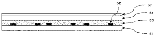
本発明の実施の形態について図33から38に基づいて説明すれば次の通りである。図33は本実施例の形態にかかる表示素子101の概略図を示す断面図である。本表示素子は基板51に発色素子を備えた構成である。
【0136】
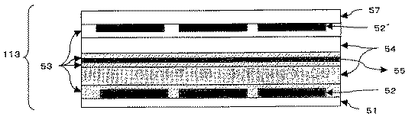
基板51は絶縁性基板からなり、本基板上にお互いに平行に配置された電極52と、電極52を覆うように形成された絶縁性機能性膜53、電界によって光学変化を起こす超分子構造体54、電極52と垂直に交差するように配置された対抗電極55、電極55と超分子構造体54の間に形成された絶縁性機能性膜56、電極55及び素子101を覆うように設置された保護膜57から構成される。
【0137】
基板51は前述の基板上に配置される部材52〜57を支持するための支持体であり、ガラスやプラスティック材料などが用いられる。この基板は部材52〜57が支持できれば良いので硬質なものである必要はない。また、後述する超分子構造体の光学変化や電極材料にもよるが、基板は透明であることが望ましい。
【0138】
電極52、55は後述する超分子構造体の光学変化にもよるが、透明であることが望ましい。この場合,電極材料としてはITOや酸化スズなどが用いられる。これらの電極は一般的にフォトリソ工程で作成されるが、素子101を基板から順次積層することによって素子を作成する場合には、有機材料上に直接電極を形成する必要がある。この場合、電極形成のためのフォトリソ工程によって有機材料を汚染する場合がある。このような場合には、後述するような転写法によっても電極を形成することができる。また、塗布型の有機錯体導電性材料もあり、このような材料の場合にはスクリーン法に代表されるような印刷法によって電極を形成してもよい。
【0139】
また、本実施形態では、電極52、55を超分子構造体54を上下にはさむように配置したが、図34のように同一平面上に設置する方法もある。この方法では有機材料上に電極を作成する必要が無いので電極作成時にすでに形成された有機材料を侵食することなく素子を作成することができる。
【0140】
また、本実施形態では単純マトリックス駆動方式による素子構造を示したが、アクティブマトリックス駆動に対応する素子にすることもできる。
絶縁性機能性材料53、56は電極52、55と超分子構造体54を結びつけるために配置される。ここで機能性膜とは、上下や左右の電極間が導電しないような絶縁性や、超分子構造体の機能性を向上させるため超分子構造体を配列させる配向制御膜、超分子構造体に効率よく電荷を注入する為の電荷注入層などが考えられる。また、電極からかけられる電界の効果を超分子構造体に効率よく伝達できるインターフェイス機能を有する膜でもよい。機能性材料はこれらに限定されるわけでもなく、光学変化を起こす超分子構造体の機能性向上をもたらすものであればよい。特に機能性膜53、56が必要でなければ、これら機能性膜は設置することもないし、逆に必要であれば数層の機能性膜を積層して設置してもよい。
【0141】
機能性膜53、56は、上下基板で同じ機能性膜を持った同じ膜を用いてもいいし、上下で機能性の異なる膜を形成してもよい。これらの機能性膜は通常有機材料が用いられるが、無機材料でもいいし、無機材用と有機材料をハイブリッドさせた材料でもよい。これらの機能性膜は、蒸着法、スピンコート法、キャスト法、印刷法、LB膜法など公知の方法で膜形成することができる。
【0142】
保護層57は、電極55上に形成される。保護膜は、超分子構造体や機能性膜が外部の酸素や水分に触れることによって機能性を低下することを防いだり、素子を外的な衝撃から防護する機能性を持つ。そのため保護層としては、これらの機能性膜は通常有機材料が用いられるが,無機材料でもいいし、無機材用と有機材料をハイブリッドさせた材料でもよい。これらの機能性膜は、蒸着法、スピンコート法、キャスト法、印刷法、LB膜法など公知の方法で膜形成することができる。
【0143】
また、超分子構造体54が溶液系、あるいはゲル状流動体である場合には、基板51のみでは超分子構造体54を支持できない場合がある。このような場合には保護層57も基板51同様支持体として機能する材料にする必要がある。このようにして、上下を支持基板で支持し、側面部を有機樹脂などで封止することによって素子101を作成することができる。ここで支持材料は基板51と同様の材料を用いることができる。封止材料としては超分子構造体や電極材料機能性膜などへの悪影響が最小限に止められる材料であることが望ましい。材料としては液晶表示素子の封止材として用いられるような有機系接着剤などが挙げられるがこれに限るものではない。
【0144】
超分子構造体54の種類とそれによって作成される素子101の種類については後述する。
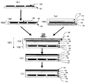
次に、素子101のプロセス方法について説明する。ここでは実施の一例として転写法を用いた素子の作成方法を示すが、素子の作成方法がこの方法に限定されるものではない。
(転写法による素子101の作成方法)
ここでは素子101を基板51上に各部材52から57を順次積層して作成する。まずプラスティック基板51上にITOをスパッタリング法で製膜した(図35(a))。ここでプラスチック基板は吸水性が押さえられ、またフォトリソプロセス(露光、現像、エッチングなど)によって侵食されない材料を用いている。また、ITOの厚さは1000Åとした。これをフォトリソ工程で画素部280μm、抜き20μmのピッチでパターンニングした。
【0145】
このようにして形成したITO電極52上に機能性膜53を製膜した(図35(b))。ここで基板102ができる。
一方、転写基板12上に転写剥離層59を形成した(図35(c))。この転写犠牲層は、特定の紫外線を当てると転写基板から剥離する特性をもつ。このような転写犠牲層は、紫外線によって剥離作用が起こるものだけでなく、レーザー加熱によって融解するものもある。この転写犠牲層上に電極52同様にフォトリソ工程でパターンニングし電極55とした。こうして得られた電極55上に、機能性膜56及び超分子構造体54を製膜した。機能製膜53、56、超分子構造体54は用いる材料によって製膜方法が異なるので省略する。このようにして転写基板103が完成した。
【0146】
このようにして得られた転写基板103と基板102を電極2、5が互いに垂直に交差するように向かい合わせ加圧する(図35(d))。そこで転写基板裏側から紫外線を照射し転写犠牲層を剥離させる。こうして転写基板上に形成した層を基板102に転写することができる(図35(e))。こうして得られた基板104に保護層を形成した(図35(f))。保護層は、吸水性の少ない封止性の良いポリカーボネート系樹脂系材料をキャスト法によって形成した。ここで用いた有機層(機能性膜、超分子構造体、保護層)は、全て透明であり透明な素子101が完成した。
【0147】
基板51上に部材52から57を順次積層した場合には、機能性膜や超分子構造体上にITOのスパッタリング(200℃前後)及びフォトリソ工程を行う必要がある。有機機能性樹脂上にこのようなプロセスを行った場合有機樹脂が侵食され機能性を損なう可能性が高い。しかしながら上記の転写プロセスを用いることで、有機樹脂上にフォトリソプロセスを行う必要がなくなり有機樹脂の機能をそこなうことなく素子を作成することができる。またITO製膜時の高温にさらされることなく有機樹脂膜を作成することができるので、低温プロセスも可能である。
【0148】
このようにして得られた素子101は上下電極に適宜な電界を印加することによって超分子構造体の光学変化を起こし表示素子となる。以下に、電界印加によって起こる相互作用変化と光学変化及び表示素子の種類を説明する。
(表示素子の例1)
ここでは、超分子構造体54の材料として電界印加によって環状化合物が鎖状化合物から解離する特性をもつ超分子構造体A(環状化合物としてシクロデキストリンを用い、鎖状化合物としてアルキル鎖を用いたもの)を用いた。超分子構造体Aは、包接時には透明、解離時に発色する特性を有する。発色は分子設計によってCMY3色の発色特性をもつ3つの超分子構造体を作成した。また、本超分子構造体Aはポリマーフィルム化されキャスト法で塗布可能である。
【0149】
この材料を表示素子101の超分子構造体54の層として用いた。
また、ここでは機能性膜53、56として、超分子構造体Aが基板に対して垂直に配向させることができる配向制御膜を用いた。
【0150】
このようにして得られた表示素子101は、電界印加によって透明−発色のSWを行った。発色性は超分子構造体そのものが発色反応するために非常に鮮やかで見やすい素子ができた。また、消費電力も非常に小さい素子ができた。
【0151】
つぎに、CMY3色発色できるカラー表示素子を作成するため図36に示すような単色表示素子を3層積層した積層型減法混色表示素子を作成した。これは各単色発色素子104、105、106を積層したものである。各素子間は保護層57を積層している。また、背面に白色反射板60をつけ反射型素子とした。本素子は転写法によって任意に積層できるため、長分子構造体や機能性膜を侵食することなく、素子を作成することができた。
【0152】
このようにして得られた素子107は、3層透明時に背面が見えるので白表示、3層発色時に黒表示とした。さらに、各層の発色性を制御することで任意の色表示を行うことが可能である。
【0153】
こうして得られたカラー表示素子は発色が鮮やかで非常に視認性の優れた素子となった。また、色表示および白表示が非常に明るい素子となった。他の反射型素子と比べてみると、反射型液晶表示素子に比べて、本表示素子は偏向板を用いていないことやカラーフィルター並列による利用効率の低下などを起こさない積層の減法混色素子であることによって約6倍の明るさを実現することができた。また、本素子と同様の構造であるコレステリック液晶の積層素子に比べても、コレステリック液晶が螺旋ピッチによって半分の光を利用できないので、本素子は2倍の明るさを持つに至った。
【0154】
このように、現行の表示素子に比べて非常に明るく視認性に優れた素子を作成することができた。
ここでは、発色タイプの表示素子を作成したが、超分子構造体の解離−包接現象では、散乱、屈折率変化、発光などさまざまな光学変化を起こすことができるので、これらの光学特性変化に応じた素子を作成することができる。また、セル構成についても、ここで作製した積層タイプでなくても、加法混色を用いた3色並列型のカラー素子など必要に応じた素子構造をもつことができる。
(表示素子の例2)
ここでは、超分子構造体54の材料として電界印加によって環状化合物が鎖状化合物上を移動し、相互作用を起こす位置を変化させる特性をもつ超分子構造体B(環状化合物としてシクロデキストリンを用い、鎖状化合物としてアルキル鎖を用いたもの)を用いた。超分子構造体Bは、相互作用を起こす個所によって透明、発色する特性を有する。発色は分子設計によってCMY3色の発色特性をもつ3つの超分子構造体を作成した。また、本超分子構造体Bはポリマーフィルム化されキャスト法で塗布可能である。
【0155】
この材料を表示素子101の超分子構造体54の層として用いた。
また、ここでは機能性膜53、56として、超分子構造体Aが基板に対して垂直に配向させることができる配向制御膜を用いた。
【0156】
このようにして得られた表示素子101は電界印加によって透明−発色のSWを行った。発色性は超分子構造体そのものが発色反応するために非常に鮮やかで見やすい素子ができた。また、消費電力も非常に小さい素子ができた。
【0157】
ここで得られた素子は、表示素子の例1に比べて、応答速度の速い素子を作製することができた。これは例1で用いられた超分子構造体Aは、スイッチングのたびに環状化合物が鎖状化合物から解離するので、応答に時間がかかるからである。これに対して超分子構造体Bは、鎖状化合物上を環状化合物が移動するのみでスイッチングするので応答速度が速くなった。
【0158】
さらに、長時間駆動させたところ、例1の超分子構造体Aに比べてスイッチングの安定性が良かった。これも、解離−包接によってばらばらになった分子が必ずしも同じ分子同士で包接−解離を起こさないので系でのスイッチングが不均一になったためである。また、さらに素子の安定性を高めるため、超分子構造体Bの鎖状化合物の両末端にストッパー基を導入した超分子構造体Cを作製し素子に用いたところ、長時間駆動に対する安定性が向上した。これはストッパーによって、環状化合物が鎖状化合物から離脱することがなくなったため、スイッチングの安定性がさらに向上したためであると考えられる。
【0159】
また、超分子構造体の発色特性は変えることなく、鎖状化合物上に配置する環状化合物の数を増やすとともに、数種類にした超分子構造体D(環状化合物としてシクロデキストリンを用い、鎖状化合物としてアルキル鎖を用いたもの)を作製し、素子に用いたところ電界に対する発色の閾値電圧が向上した。また、閾値電圧によって発色の程度を容易に制御することができた。これは、環状化合物の数を増やすことで、発色現象の閾値がはっきり出たためで、外部の環境変化などでスイッチングが進まない安定した素子になった。また、異なる環状化合物の数が入ったため、閾値にばらつきが生じ、階調表示が制御しやすくなったと考えられる。同様に、鎖状化合物の長さを変えた超分子構造体を作成したときも、上記と同様に階調表示の制御しやすい素子を作成することができた。
【0160】
つぎに、CMY3色発色できるカラー表示素子を作成するため、表示素子の例1同様の図36に示すような単色表示素子を3層積層した積層型減法混色表示素子を作成した。
【0161】
こうして得られたカラー表示素子107は発色が鮮やかで非常に視認性の優れた素子となった。また、色表示および白表示が非常に明るい素子となった。他の反射型素子と比べてみると、反射型液晶表示素子に比べて、本表示素子は偏向板を用いていないことやカラーフィルター並列による利用効率の低下などを起こさない積層の減法混色素子であることによって約6倍の明るさを実現することができた。また、本素子と同様の構造であるコレステリック液晶の積層素子に比べても、コレステリック液晶が螺旋ピッチによって半分の光を利用できないので、本素子は2倍の明るさを持つに至った。
【0162】
このように、現行の表示素子に比べて非常に明るく視認性に優れた素子を作成することができた。さらには素子の例1に比べても応答速度、信頼性、寿命、階調表示特性の優れた表示素子を作製することができた。
【0163】
ここでは、発色タイプの表示素子を作成したが、そのほかにも発光などさまざまな光学変化を起こすことができるので、これらの光学特性変化に応じた素子を作成することができる。また、セル構成についても、ここで作製した積層タイプでなくても、加法混色を用いた3色並列型のカラー素子など必要に応じた素子構造をもつことができる。
(表示素子の例3)
ここでは、超分子構造体54の材料として電界印加によって環状化合物が鎖状化合物上の末端部分から移動し、相互作用変化を起こす特性をもつ超分子構造体E(環状化合物としてシクロデキストリンを用い、鎖状化合物としてアルキル鎖を用いたもの)を用いた。超分子構造体Eは末端部で相互作用を起こす際に発色、電界によって離脱したときに透明になる特性を有する。発色は分子設計によってCMY3色の発色特性をもつ3つの超分子構造体を作成した。また、本超分子構造体Eはポリマーフィルム化されキャスト法で塗布可能である。
【0164】
この材料を表示素子101の超分子構造体54の層として用いた。
また、ここでは機能性膜53、56として、超分子構造体Aが基板に対して垂直に配向させることができる配向制御膜を用いた。
【0165】
このようにして得られた表示素子101は電界印加によって透明−発色のSWを行った。発色性は超分子構造体そのものが発色反応するために非常に鮮やかで見やすい素子ができた。また、消費電力も非常に小さい素子ができた。
【0166】
ここで得られた素子は、表示素子の例2に比べて、応答速度の速い素子を作製することができた。超分子構造体Bは、鎖状化合物上を環状化合物が移動するのみでスイッチングするので応答速度を超分子構造体Aに比べて高速化することができたが、鎖状化合物上には複数の環状化合物と相互作用を起こす組成部位があり環状化合物の動きを阻害してしまう。これに比べて超分子構造体Eでは鎖状化合物上の障害がないので移動を阻害する要因がなく非常に早いスイッチング挙動を実現できる。そのため、μsecオーダーでのスイッチングが可能で、動画表示を行うこともできた。
【0167】
さらに、長時間駆動させたところ、超分子構造体Eでは鎖状化合物の両末端にストッパー基が導入されていたために、環状化合物が鎖状化合物から離脱することがなくなったため前述の超分子構造体C同様、非常に安定性のよい素子とすることができた。
【0168】
また、超分子構造体D同様に鎖状化合物上に配置する環状化合物の数を増やすとともに、数種類にした超分子構造体F(環状化合物としてシクロデキストリンを用い、鎖状化合物としてアルキル鎖を用いたもの)を作製し素子に用いたところ、素子に用いたところ電界に対する発色の閾値電圧が向上した。また、閾値電圧によって発色の程度を容易に制御することができた。これは、環状化合物の数を増やすことで、発色現象の閾値がはっきり出たためで、外部の環境変化などでスイッチングが進まない安定した素子になった。また、異なる環状化合物の数が入ったため、閾値にばらつきが生じ、階調表示が制御しやすくなったと考えられる。同様に、鎖状化合物の長さを変えた超分子構造体を作成したときも、上記と同様に階調表示の制御しやすい素子を作成することができた。
【0169】
つぎに、CMY3色発色できるカラー表示素子を作成するため、表示素子の例1同様の図36に示すような単色表示素子を3層積層した積層型減法混色表示素子を作成した。
【0170】
こうして得られたカラー表示素子107は、発色が鮮やかで非常に視認性の優れた素子となった。また、色表示および白表示が非常に明るい素子となった。他の反射型素子と比べてみると、反射型液晶表示素子に比べて、本表示素子は偏向板を用いていないことやカラーフィルター並列による利用効率の低下などを起こさない積層の減法混色素子であることによって約6倍の明るさを実現することができた。また、本素子と同様の構造であるコレステリック液晶の積層素子に比べても、コレステリック液晶が螺旋ピッチによって半分の光を利用できないので、本素子は2倍の明るさを持つに至った。
【0171】
また、上記液晶表示素子では応答速度が遅いために動画表示、特に動きの速い映像では表示が汚く動画表示に適さないことがあるが、本表示素子では高速スイッチングが可能であり、動画表示も可能であった。
【0172】
このように、現行の表示素子に比べて非常に明るく視認性に優れた素子を作成することができた。さらには応答速度、信頼性、寿命、階調表示特性の優れた、動画表示も可能な表示素子を作製することができた。
【0173】
ここでは、発色タイプの表示素子を作成したが、そのほかにも発光などさまざまな光学変化を起こすことができるので、これらの光学特性変化に応じた素子を作成することができる。また、セル構成についても、ここで作製した積層タイプでなくても、加法混色を用いた3色並列型のカラー素子など必要に応じた素子構造をもつことができる。
(表示素子の例4)
ここでは、超分子構造体54の材料として電界印加によってチューブ状環状化合物内を鎖状化合物が末端部分から移動し、相互作用変化を起こす特性をもつ超分子構造体G(環状化合物としてシクロデキストリンを用い、鎖状化合物としてアルキル鎖を用いたもの)を用いた。環状化合物はチューブ状であり末端部に鎖状化合物と相互作用を起こす誘導基を有している。超分子構造体Gは末端部で相互作用を起こす際に発色、電界によって離脱したときに透明になる特性を有する。発色は分子設計によってCMY3色の発色特性をもつ3つの超分子構造体を作成した。また、本超分子構造体Fはポリマーフィルム化されキャスト法で塗布可能である。
【0174】
この材料を表示素子101の超分子構造体54の層として用いた。
また、ここでは機能性膜53、56として、超分子構造体Aが基板に対して垂直に配向させることができる配向制御膜を用いた。
【0175】
このようにして得られた表示素子101は電界印加によって透明−発色のSWを行った。発色性は超分子構造体そのものが発色反応するために非常に鮮やかで見やすい素子ができた。また、消費電力も非常に小さい素子ができた。
【0176】
ここで得られた素子は、表示素子の例3同様、応答速度の速い素子を作製することができた。超分子構造体Gは、チューブ状環状化合物内を鎖状化合物が移動するのみでスイッチングし、環状内には鎖状化合物の移動を阻害する障害がないので非常に早いスイッチング挙動を実現できる。そのため、μsecオーダーでのスイッチングが可能で、動画表示を行うこともできた。
【0177】
さらに、長時間駆動させたところ、超分子構造体Gでは環状化合物内を動くために、環状化合物外の変化や他分子の影響を受けることがないので、非常に安定性のよい素子とすることができた。
【0178】
つぎに、CMY3色発色できるカラー表示素子を作成するため、表示素子の例1同様の図36に示すような単色表示素子を3層積層した積層型減法混色表示素子を作成した。
【0179】
こうして得られたカラー表示素子107は、発色が鮮やかで非常に視認性の優れた素子となった。また、色表示および白表示が非常に明るい素子となった。他の反射型素子と比べてみると、反射型液晶表示素子に比べて、本表示素子は、偏向板を用いていないことやカラーフィルター並列による利用効率の低下などを起こさない積層の減法混色素子であることによって、約6倍の明るさを実現することができた。また、本素子と同様の構造であるコレステリック液晶の積層素子に比べても、コレステリック液晶が螺旋ピッチによって半分の光を利用できないので、本素子は2倍の明るさを持つに至った。
【0180】
また、上記液晶表示素子では応答速度が遅いために動画表示、特に動きの速い映像では表示が汚く動画表示に適さないことがあるが、本表示素子では高速スイッチングが可能であり、動画表示も可能であった。
【0181】
このように、現行の表示素子に比べて非常に明るく視認性に優れた素子を作成することができた。さらには応答速度、信頼性、寿命、などの特性の優れた、動画表示も可能な表示素子を作製することができた。
【0182】
ここでは、発色タイプの表示素子を作成したが、そのほかにも発光などさまざまな光学変化を起こすことができるので、これらの光学特性変化に応じた素子を作成することができる。また、セル構成についても、ここで作製した積層タイプでなくても、加法混色を用いた3色並列型のカラー素子など必要に応じた素子構造をもつことができる。
(表示素子の例5)
ここでは、超分子構造体54の材料として電界印加によって環状化合物が鎖状化合物上の末端部分から移動し、相互作用変化を起こす特性をもつ超分子構造体H(環状化合物としてシクロデキストリンを用い、鎖状化合物としてアルキル鎖を用いたもの)を用いた。超分子構造体Hは末端部で相互作用を起こす際に発色、電界によって離脱したときに透明になる特性を有する。発色は分子設計によってCMY3色の発色特性をもつ3つの超分子構造体を作成した。また、本超分子構造体Hはポリマーフィルム化されキャスト法で塗布可能である。
【0183】
さらに、電界印加によって環状化合物が鎖状化合物上の末端部分から移動し、相互作用変化を起こす特性をもつ超分子構造体I(環状化合物としてシクロデキストリンを用い、鎖状化合物としてアルキル鎖を用いたもの)を用いた。超分子構造体Iは、末端部で相互作用を起す際に発光し、電界によって離脱したときに透明になる特性を有する。発色は分子設計によってCMY3色の発色特性をもつ3つの超分子構造体を作成した。また、本超分子構造体Hはポリマーフィルム化されキャスト法で塗布可能である。
【0184】
発光色は、分子設計によってRGB3色の発色特性をもつ3つの超分子構造体を作成した。また、本超分子構造体Iは、ポリマーフィルム化されキャスト法で塗布可能である。
【0185】
ここで、H、Iは、電界極性に対する特性を逆方向にした。つまり、相互作用を起す末端部分に対して、超分子構造体Hは+極性を印加したときに環状化合物が離脱し消色する。逆に、超分子構造体Iにおいては−極性を印加したときに環状化合物が離脱し発光が消える。
【0186】
このような特性をもつ材料を混合させ、表示素子101の超分子構造体54の層として用いた。
また、ここでは機能性膜53、56として、超分子構造体H、Iが基板に対して垂直に配向させることができる配向制御膜を用いた。また、この配向制御膜では図37に示すように超分子構造体H、Iいずれの材料についても鎖状化合物の発色相互作用基61、発光相互作用基62の末端が同じ電極方向に配列するように配向制御させた。
【0187】
このようにして得られた表示素子101は電界印加によって、発光、発色の2種類の表示形態を発現させることができる。電極を反転させることによって、透明−発色のSWと透明−発光のSWを起すことができる。
【0188】
このように、極性反転によって発光と発色を使い分けることができれば、1表示素子において発光ディスプレイと、反射型ディスプレイを同時に作製することができる。このようなディスプレイは、証明環境の違いに応じて最適な視認性を得るディスプレイとなり、マルチシーンで使用可能なディスプレイである。昼間のように外光が明るい時は反射型ディスプレイとして、夜間時は発光型ディスプレイとして用いることができる。また、文字情報や静止画情報などを見る場合には目にやさしい反射型ディスプレイとして、臨場感のある動画映像を見る場合には発光型ディスプレとして用いることができる。
【0189】
本表示素子においても、照明環境や、画像の種類によって電極を入れ替えることで反射型、発光型を任意に切り替えることができるので、マルチシーンディスプレイとして用いることができた。また、電極の構成や、駆動方法によっては表示素子の画面の一部を反射型、一部を発光型にできるので、文字コンテンツの一部が映像情報でそのコンテンツに応じた表示方法を選択することができる。
【0190】
ここで得られた素子は、発色、発光どちらの表示形態においても、応答速度の速い素子を作製することができた。超分子構造体H、Iでは鎖状化合物上の障害がないので移動を阻害する要因がなく非常に早いスイッチング挙動を実現できる。そのため、μsecオーダーでのスイッチングが可能で、動画表示を行うこともできた。
【0191】
さらに、長時間駆動させたところ、超分子構造体H、Iでは鎖状化合物の両末端にストッパー基が導入されているので、環状化合物が鎖状化合物から離脱することがなくなったため前述の超分子構造体C同様、非常に安定性のよい素子とすることができた。
【0192】
また、超分子構造体D、F同様に鎖状化合物上に配置する環状化合物の数を増やすとともに、数種類にしたところ、素子に用いたところ電界に対する閾値電圧が向上した。また、閾値電圧によって階調表示を容易に制御することができた。これは、環状化合物の数を増やすことで、発色現象の閾値がはっきり出たためで、外部の環境変化などでスイッチングが進まない安定した素子になった。また、異なる環状化合物の数が入ったため、閾値にばらつきが生じ、階調表示が制御しやすくなったと考えられる。
つぎに、カラー表示素子を作成するため、表示素子の例1同様の図36に示すような単色表示素子を3層積層した積層型表示素子を作成した。
【0193】
こうして得られたカラー表示素子107は、極性によって発光素子と発色素子を使い分けることができ、さらに電界の強度によって発光強度や発色の程度を制御できるマルチシーンディスプレイとなった。
【0194】
ここでは、極性によって発色、発光を制御する表示素子を作製したが、発色、発光の閾値電圧に差をもたすことでも2つの表示形態を制御することは可能である。
【0195】
また、ここでは2種類の表示形態をもつ超分子構造体の混合でマルチシーンディスプレイという多機能ディスプレイを作製したが、発色色相の異なる超分子構造体、発光色の異なる超分子構造体を混入させたものでも多機能表示素子を作製することができる。
(表示素子の例6)
ここでは、超分子構造体54の材料として電界印加によって環状化合物が鎖状化合物上の末端部分から移動し、相互作用変化を起こす特性をもつ超分子構造体J(環状化合物としてシクロデキストリンを用い、鎖状化合物としてアルキル鎖を用いたもの)を用いた。超分子構造体Jは鎖状化合物の両末端に相互作用を起す誘導基を有している。さらに片方の末端部では相互作用を起こす際に発色、電界によって離脱したときに透明になる特性を有する。さらに、もう片方の末端部で相互作用を起す際に発光し、電界によって離脱したときに透明になる特性を有する。また、各末端で相互作用から環状化合物を離脱させるための電界極性が反対極性である特性を持つ。
【0196】
つまり、電界によって鎖状化合物の両末端まで環状化合物を移動させ、電界の極性によって両末端を選択制御し極性によって発色と発光を制御することができる。
【0197】
発色は、分子設計によってCMY3色の発色特性をもつ3つの超分子構造体を作成した。また、発光色は分子設計によってRGB3色の発色特性をもつ3つの超分子構造体を作成した。発色は分子設計によってCMY3色の発色特性をもつ3つの超分子構造体を作成した。また、本超分子構造体Jは、ポリマーフィルム化されキャスト法で塗布可能である。
【0198】
このような特性をもつ材料を混合させ、表示素子101の超分子構造体54の層として用いた。
また、ここでは機能性膜53、56として、超分子構造体Jが基板に対して垂直に配向させることができる配向制御膜を用いた。また、この配向制御膜では超分子構造体Jについて図38に示すように、鎖状化合物の発色相互作用基61と、発光相互作用基62が同方向に配列するように配向制御させた。
【0199】
このようにして得られた表示素子101は電界印加によって、発光、発色の2種類の表示形態を発現させることができる。電極を反転させることによって、透明−発色のSWと透明−発光のSWを起すことができる。
【0200】
このように、極性反転によって発光と発色を使い分けることができれば、1表示素子において発光ディスプレイと、反射型ディスプレイを同時に作製することができる。このようなディスプレイは、証明環境の違いに応じて最適な視認性を得るディスプレイとなり、マルチシーンで使用可能なディスプレイである。昼間のように外光が明るい時は反射型ディスプレイとして、夜間時は発光型ディスプレイとして用いることができる。また、文字情報や静止画情報などを見る場合には目にやさしい反射型ディスプレイとして、臨場感のある動画映像を見る場合には発光型ディスプレイとして用いることができる。
【0201】
本表示素子においても、照明環境や、画像の種類によって電極を入れ替えることで反射型、発光型を任意に切り替えることができるので、マルチシーンディスプレイとして用いることができた。また、電極の構成や、駆動方法によっては表示素子の画面の一部を反射型、一部を発光型にできるので、文字コンテンツの一部が映像情報でそのコンテンツに応じた表示方法を選択することができる。
【0202】
ここで得られた素子は、発色、発光どちらの表示形態においても、応答速度の速い素子を作製することができた。超分子構造体Jでは鎖状化合物上の障害がないので移動を阻害する要因がなく非常に早いスイッチング挙動を実現できる。そのため、μsecオーダーでのスイッチングが可能で、動画表示を行うこともできた。
【0203】
さらに、長時間駆動させたところ、超分子構造体Jでは鎖状化合物の両末端にストッパー基が導入されているので、環状化合物が鎖状化合物から離脱することがなくなったため、前述の超分子構造体C同様、非常に安定性のよい素子とすることができた。
【0204】
また、超分子構造体D、F同様に鎖状化合物上に配置する環状化合物の数を増やすとともに、数種類にしたところ、素子に用いたところ電界に対する閾値電圧が向上した。また、閾値電圧によって階調表示を容易に制御することができた。これは、環状化合物の数を増やすことで、発色現象の閾値がはっきり出たためで、外部の環境変化などでスイッチングが進まない安定した素子になった。また、異なる環状化合物の数が入ったため、閾値にばらつきが生じ、階調表示が制御しやすくなったと考えられる。
【0205】
表示素子の例5では、同一画素に異なる2種類の表示形態を有する超分子構造体H、Iを混合してマルチシーンディスプレイとした。この場合、2種類の超分子構造体はほぼ均一に混合され画素のむら等はなかったが、材料系によっては分離が起こり不均一な表示になってしまう可能性がある。しかしながら、本例では1分子内で発色と発光という2つの機能性があることから材料の混合むらや層分離といった問題のない表示の均一な表示素子を作製することができた。
【0206】
つぎに、カラー表示素子を作成するため、表示素子の例1同様の図36に示すような単色表示素子を3層積層した積層型表示素子を作成した。
こうして得られたカラー表示素子107は、極性によって発光素子と発色素子を使い分けることができ、さらに電界の強度によって発光強度や発色の程度を制御できるマルチシーンディスプレイとなった。
【0207】
ここでは2種類の表示形態をもつ超分子構造体によってマルチシーンディスプレイという多機能ディスプレイを作製したが、発色色相の異なる超分子構造体、発光色の異なる超分子構造体を混入させたものでも多機能表示素子を作製することができる。
実施形態2・インプレイン素子
以下、本発明の実施の形態の1例を詳細に説明するが、本発明が以下に実施例に限定されるものではない。
【0208】
なお、説明の便宜上前述の実施の形態の図面に示した部材と同一の部材には同一の符号を付記しその説明を省略する。
本発明の他の実施の形態について図39から41に基づいて説明すれば次の通りである。図39は、本実施例の形態にかかる表示素子108の概略図を示す断面図である。本表示素子は、基板51に発色素子を備えた構成である。
【0209】
基板51は絶縁性基板からなり、本基板上にお互いに平行に配置された電極52と、電極52を覆うように形成された絶縁膜53、電極52と平行に形成された電極55、電界によって光学変化を起こす超分子構造体54、電極55及び素子101を覆うように設置された保護膜57から構成される。
【0210】
電極52及び55は図40に示すように、まずお互いが平行で電極55に対して垂直な方向に伸びたライン及び画素部を形成する電極55に平行なラインを備えたくし型電極を形成する。得られたくし型電極を覆うように絶縁膜63を形成し、さらにその上に電極55を電極52のくし歯と平行に形成することで電極52と55を形成しこれらの電極に囲まれた64が画素領域となる。ここでは、単純間トリック上の電極構造としたが、インプレイン用のアクティブ素子を用いた電極構造にしてもよい。
【0211】
ここでは、表示素子108を基板51上への順次積層プロセスによって形成した。本表示素子では電極構造がインプレイン型であるので、電極構造を作製した後では、機能膜53、超分子構造体54、保護膜57を順次積層するだけで表示素子とすることができる。これらの有機系膜上に電極形成プロセスなどを行うことがなく、有機膜表面や内部を侵食されることのない表示素子を作成することができる。
【0212】
このようにして作製した、表示素子108に対して、超分子構造体54として前述の実施の形態で挙げたような材料を用いた。機能膜53については電界のかかる方向は横方向であるので超分子構造体を基板に対して平行方向に配向させた。さらに、分子の向きも電界効果が向上するように同一方向に配列した。また、横電極によって電極間は分子長に対して非常に長くなってしまうので、電界の効果を高めるように機能膜53に電荷輸送効果のある成分を混合することで素子の性能を向上させる材料もあった。
【0213】
超分子構造体54は、本表示素子でも前述の実施の形態1と同じようにスイッチング挙動を起し表示素子として機能した。
さらに、図41に示すような単層発色素子109、110、111を積層して作製した表示素子112においても実施の形態1同様にカラー表示素子として、従来の反射型ディスプレイに比べて非常に明るいディスプレイを作製することができた。しかしながら、本形態では、表示素子107に比べて電極の開口率が小さいため、107に比べてやや暗い表示素子となった。
【0214】
また、実施の形態例5、6におけるマルチシーンディスプレイの形態も同じ材料系で同様の表示を行うことができた。
このように、インプレイン構造によっても従来の表示素子より優れた性能を有する表示素子を作製することができた。
実施形態3・多機能表示素子
以下、本発明の実施の形態の1例を詳細に説明するが、本発明が以下に実施例に限定されるものではない。
【0215】
なお、説明の便宜上前述の実施の形態の図面に示した部材と同一の部材には同一の符号を付記しその説明を省略する。
本発明の他の実施の形態について図42に基づいて説明すれば次の通りである。図42は、本実施例の形態にかかる表示素子113の概略図を示す断面図である。本表示素子は基板51に発色素子を備えた構成である。
【0216】
基板51は絶縁性基板からなり、本基板上にお互いに平行に配置された電極52と、電極52を覆うように形成された絶縁性機能性膜53、電界によって光学変化を起こす超分子構造体54、電極52と垂直に交差するように配置された対抗電極55、電極55と超分子構造体54の間に形成された絶縁性機能性膜53、さらに超分子構造体54’さらにその上に電極52と平行かつ同じ形状に形成された電極52’及び素子113を覆うように設置された保護膜57から構成される。
【0217】
本構成の表示素子113は、実施の形態1で示した転写法によって、有機系膜上に電極プロセスが行われないように作製された。
こうして得られた表示素子113に超分子構造体54として前述の実施の形態1で挙げたような材料を用いた。
【0218】
この構成では、2層の長分子構造体層に中心の電極55を標準電位として用いることで、同時に電極をかけることができる。
超分子構造体54および54’に同一の超分子構造体を用いたところ、2層によって発色を制御できるので、単一の材料では制御が難しいものでも階調表示を容易に制御することができた。
【0219】
超分子構造体54および54’に片側に発光材料、片方に発色材料を用いたところ、2層同時制御によって発光と発色を同時に制御することができる。実施の形態1の表示素子の例5、6では超分子構造体H、Iの混合体、超分子構造体Jが極性反転や電界の閾値に大きな差がなければ2つの表示形態をコントロールできなかったが、ここでは独立に、しかも同時に駆動できるので表示形態の特性差がなくても制御することができる。また、発色させ、同時に発光させることも可能でありさらに多彩な表示形態を作り出すことができる。
【0220】
このように、本実施の形態によって多機能表示素子を作成することができる。
実施形態4・画素分割表示素子
以下、本発明の実施の形態の1例を詳細に説明するが、本発明が以下に実施例に限定されるものではない。
【0221】
なお、説明の便宜上前述の実施の形態の図面に示した部材と同一の部材には同一の符号を付記しその説明を省略する。
本発明の他の実施の形態について図43に基づいて説明すれば次の通りである。図43は、本実施例の形態にかかる表示素子114の概略図を示す断面図である。本表示素子は基板51に発色素子を備えた構成である。
【0222】
本構成は実施の形態1と同様であるが、電極52が1画素内で分割されてそれぞれを独立に駆動できるところが異なっている。
本構成によって、実施の形態1で用いた超分子構造体54を用いたところ、分割されていない画素による駆動では電界の強弱によって階調表示を制御することが難しかった材料でも、分割画素による独立駆動によって画素分割階調表示を行うことができた。また、応答速度が高速である利点を生かして、時間分割による階調表示と組み合わせるとさらに細かい階調表示が可能となる。
【0223】
また、本構成によって、実施の形態1例5、6で用いた超分子構造体H、Iの混合体、超分子構造体Jを用いたところ、画素内のそれぞれの分割画素で電極を反転制御することで、発光、発色が可能なマルチシーン表示素子を作製することができた。実施の形態1の表示素子の例5、6では超分子構造体H、Iの混合体、超分子構造体Jが極性反転や電界の閾値に大きな差がなければ2つの表示形態をコントロールできなかったが、ここでは独立に、しかも同時に駆動できるので表示形態の特性差がなくても制御することができる。さらに、発光と発色表示を同時に行うこともできるので、さらに多機能な表示も可能である。
【0224】
さらに、図44に示すように、各分割画素ごとに異なる超分子構造体を転写法によって形成することで、分割画素それぞれを独立させ1画素において多機能な表示機能を持たせることができる。ここでは、2分割した画素に発光及び発色材料を転写法によって作製したところ、画素内のそれぞれの分割画素で電極を制御することで、発光、発色が可能なマルチシーン表示素子を作製することができた。上述した素子同様に、ここでも各分割画素を独立にしかも同時に駆動できるので、表示形態の特性差がなくても制御することができる。
【0225】
このように、画素分割を行いそれぞれを独立駆動することで、階調表示や多機能表示素子を作製することができた。
【0226】
【発明の効果】
本発明の第1の態様における表示素子または調光素子は、環状化合物と前記環状化合物に包接された鎖状化合物からなる超分子構造体と、前記超分子構造体を少なくとも1枚の支持基板と封止材料に狭持された素子からなり、超分子構造体の1状態として上記鎖状化合物が環状化合物を貫通できるロタキサン構造体を持ち、鎖状化合物上を環状化合物が移動することができ、外部刺激によって環状化合物の移動を制御することで、上記超分子体の相互作用変化を起こし光学特性を変化させる構成である。この構成により、超分子構造体のスイッチングを用いた新規な表示素子を提供できる。
【0227】
本発明の第2の態様における表示素子または調光素子は、第1の態様の構成において、上記超分子構造体が上記鎖状化合物が環状化合物を貫通できるロタキサン構造体であり、かつ鎖状化合物の少なくとも一端に前記環状化合物が鎖状化合物から脱離できないような置換基が導入されている構成である。この構成により、分子シャトルによるスイッチング原理に基づく新規な表示素子を提供できる。本発明の第3の態様における表示素子または調光素子は、第1の態様の構成において、上記相互作用変化が、環状化合物と鎖状化合物が包接状態と解離状態をとる構成である。この構成によって、超分子構造体の包接−解離現象によるスイッチング原理に基づく新規な表示素子を提供できる。
本発明の第4の態様における表示素子または調光素子は、第1及び第2の態様の構成において上記相互作用変化が、環状化合物の鎖状化合物上における停止位置変化である構成である。この構成によって、超分子の分子シャトル移動によるスイッチング原理に基づく新規な表示素子、特に、応答速度や素子の安定性に優れた表示素子を提供できる。
本発明の第5の態様における表示素子または調光素子は、第2の態様の構成において、上記相互作用変化が末端部と環状化合物との相互作用による鎖状化合物上移動である構成である。この構成によって、超分子の分子シャトル移動によるスイッチング原理に基づく新規な表示素子特に動画表示可能な応答速度を持ち、さらにセルの信頼性に優れた表示素子を提供することができる。
本発明の第6の態様における表示素子または調光素子は、第1から第5の態様の構成において上記支持基板が電極を備え、電気的刺激によって上記超分子構造体の相互作用を制御する構成である。この構成によって、表示の書き換え、さらには動画表示を任意に行うことができ、及び超分子構造体のシャトル移動駆動力として働くことができる。
本発明の第7の態様における表示素子または調光素子は、第6の態様の構成において電気的刺激を上記支持基板に対して上下から与える構成である。この構成によって、表示の書き換え、さらには動画表示を任意に行うことができ、特に均一な電気刺激を与えることができる。
本発明の第8の態様における表示素子または調光素子は、第6の態様の構成において上記電気的刺激を上記支持基板に対して同一平面上から与える構成である。この構成によって、表示の書き換え、さらには動画表示を任意に行うことができ、特に有機構成膜を侵すことなく表示素子を作成できる。
本発明の第9の態様における表示素子または調光素子は、第1から第6の態様の構成において上記超分子構造体が上記基板に対して略垂直または略並行に配向している構成である。この構成によって、外部刺激の効果を効果的に伝達し超分子構造体の光学特性変化を効果的に発現させることができる。
【0228】
本発明の第10の態様における表示素子または調光素子は、第1から第9の態様の構成において上記超分子構造体が単一分子内で相互作用変化および光学変化を完結する構成である。この構成によって、超分子構造体の光学特性変化を効果的に発現させ、さらには信頼性に優れた表示素子を提供することができる。
【0229】
本発明の第11の態様における表示素子または調光素子は、第1から第10の態様の構成において、上記素子が電極と超分子構造体間に少なくとも一層以上の中間層を含む構成である。この構成によって、光学特性変化を効果的に発現させることができる。
【0230】
本発明の第12の態様における表示素子または調光素子は、第11の態様の構成において、上記機中間層が電極と超分子構造体間に設置され、電界印加時の電極と超分子構造体間のインターフェイスとして機能する構成である。この構成によって、電極からの電気刺激を効果的に超分子構造体に伝達し、超分子構造体の光学特性変化を効果的に発現させることができる。
【0231】
本発明の第13の態様における表示素子または調光素子は、第1から第6の態様の構成において、上記超分子構造体を含む系が固形である構成である。この構成によって、信頼性の高い表示素子を提供することができる。
【0232】
本発明の第14の態様における表示素子または調光素子は、第1から第13の態様の構成において、上記超分子体の環状化合物が複数の環状化合物で形成されたチューブ状化合物である構成である。この構成によって、超分子構造体に外部刺激に対する閾値を持たせ信頼性の高い表示素子を提供することができる。
【0233】
本発明の第15の態様における表示素子または調光素子は、第1から第14の態様の構成において、上記超分子構造体の環状化合物が鎖状化合物中に複数個包接されている構成である。この構成によって、超分子構造体に外部刺激に対する閾値を持たせ、信頼性の高い表示素子を提供することができる。
【0234】
本発明の第16の態様における表示素子または調光素子は、第15の態様の構成において、上記環状化合物がチューブ状であり、鎖状化合物がチューブ内を移動する構成である。この構成によって、鎖状化合物の移動によるスイッチング原理に基づく新規な表示素子、特に高速応答性、高い信頼性を有する表示素子を提供することができる。
【0235】
本発明の第17の態様における表示素子または調光素子は、第1から第6の態様の構成において、上記超分子構造体は外部刺激を与えられる最小単位内に少なくとも2種類以上の異なる構成単位を持つ構成である。この構成によって、階調表示を用意に可能にする表示素子を提供することができる。
【0236】
本発明の第18の態様における表示素子または調光素子は、第1から第17の態様の構成において、上記構造体を構成する系に、少なくとも2種類以上の鎖長の異なる鎖状化合物が含まれていることを特徴としている。この構成によって、階調表示を用意に可能にする表示素子を提供することができる。
【0237】
本発明の第19の態様における表示素子または調光素子は、第1から第5の態様の構成において、上記超分子構造体の外部刺激による光学特性変化の形態が同一素子内の外部刺激の与えられる最小単位内で、少なくとも二種類以上起こる構成である。この構成によって、多機能な表示素子、特にマルチシーンディスプレイを提供することができる。
【0238】
本発明の第20の態様における表示素子または調光素子は、第1から第5の態様の構成において、上記超分子構造体が、外部刺激による光学特性変化の形態が同一分子内で少なくとも二種類以上設けられる構成である。この構成によって、多機能な表示素子、特にマルチシーンディスプレイを提供することができる。
【0239】
本発明の第21の態様における表示素子または調光素子は、第1から第20の態様の構成において、上記超分子構造体と電極から構成される素子において、1層の標準電極と前記標準電極を挟み込む少なくとも2層以上の超分子構造体、さらに前記超分子構造体の外側に設置された電極が設けられ、上記三つの電極によって同時に2層の超分子構造体を制御する構成である。この構成によって、超分子構造体の階調表示素子や多機能な表示素子を提供できる。
【0240】
本発明の第22の態様における表示素子または調光素子は、第1から第21の態様の構成において、上記超分子構造体と電極から構成される素子において、1表示画素が複数に分割されている構成である。この構成によって、超分子構造体の階調表示素子や多機能な表示素子を提供できる。
【0241】
本発明の第23の態様における表示素子または調光素子は、第1から第22の態様の構成において、上記超分子構造体と電極から構成される素子の少なくとも一部分が、転写法によって製造される構成である。この構成によって、超分子構造体や有機機能膜を侵すことなく素子構成膜を積層でき、特性を十分発揮することができる。
【図面の簡単な説明】
【図1】本発明に係る超分子構造体の例を示す図である。
【図2】本発明に係る本発明の表示素子の概略図を示す図である。
【図3】本発明に係る超分子構造体の分子シャトルの概略図を示す図である。
【図4】本発明に係る超分子構造体の包接−解離現象の1例を示す図である。
【図5】本発明に係る超分子構造体の包接−解離現象の1例を示す図である。
【図6】本発明に係る超分子構造体の包接−解離現象の1例を示す図である。
【図7】本発明に係る超分子構造体の包接−解離現象の1例を示す図である。
【図8】本発明に係る超分子構造体の包接−解離現象による光学特性の変化の1例を示す図である。
【図9】本発明に係る超分子構造体の包接−解離現象による光学特性の変化の1例を示す図である。
【図10】本発明に係る超分子構造体の包接−解離現象による光学特性の変化の1例を示す図である。
【図11】本発明に係る超分子構造体の包接−解離現象による光学特性の変化の1例を示す図である。
【図12】本発明に係る超分子構造体の包接−解離現象による光学特性の変化の1例を示す図である。
【図13】本発明に係る超分子構造体の包接−解離現象による光学特性の変化の1例を示す図である。
【図14】本発明に係る超分子構造体の分子ステーション現象の1例を示す図である。
【図15】本発明に係る超分子構造体の分子ステーション現象の1例を示す図である。
【図16】本発明に係る超分子構造体の分子ステーション現象の1例を示す図である。
【図17】本発明に係る超分子構造体の分子ステーション現象の1例を示す図である。
【図18】本発明に係る超分子構造体の末端基の相互作用の1例を示す図である。
【図19】本発明に係る超分子構造体の末端基の相互作用の1例を示す図である。
【図20】本発明に係る超分子構造体の末端基の相互作用の1例を示す図である。
【図21】本発明に係る超分子構造体の末端基の相互作用の1例を示す図である。
【図22】本発明に係る超分子構造体の末端基の相互作用の1例を示す図である。
【図23】本発明に係る超分子構造体の末端基の相互作用の1例を示す図である。
【図24】本発明に係る超分子構造体の末端基相互作用による光学変化の1例を示す図である。
【図25】本発明に係る発色団の構成を示す図である。
【図26】本発明に係る超分子構造体の末端基相互作用による光学変化の1例を示す図である。
【図27】本発明に係る電極構造の1例を示す図である。
【図28】本発明に係る電極構造の1例を示す図である。
【図29】本発明に係る電極構造の1例を示す図である。
【図30】本発明に係る超分子構造体の1例を示す図である。
【図31】本発明に係る超分子構造体の相互作用の1例を示す図である。
【図32】本発明に係る表示素子の構造の1例を示す図である。
【図33】本発明に係る実施の形態における表示素子の概略を示す図である。
【図34】本発明に係る実施の形態における表示素子の概略を示す図である。
【図35】本発明に係る実施の形態における表示素子の製造方法の1例を示す図である。
【図36】本発明に係る実施の形態における表示素子の概略を示す図である。
【図37】本発明に係る実施の形態における超分子構造体の配列の1例をを示す図である。
【図38】本発明に係る実施の形態における超分子構造体の配列の1例を示す図である。
【図39】本発明に係る実施の形態における表示素子の概略を示す図である。
【図40】本発明に係る実施の形態における電極形成方法の1例を示す図である。
【図41】本発明に係る実施の形態における表示素子の概略を示す図である。
【図42】本発明に係る実施の形態における表示素子の概略を示す図である。
【図43】本発明に係る実施の形態における表示素子の概略を示す図である。
【図44】本発明に係る実施の形態における表示素子の概略を示す図である。
【符号の説明】
1:鎖状化合物
2:環状化合物
3:誘導体
4:鎖状化合物上の異なる組成単位
5:鎖状化合物上の異なる組成単位
6:基板
7:超分子構造体
8:封止材料
9:対抗基板
10:側面封止材料
11:区画化材料
12:ストッパー
13:交換鎖状化合物
14:媒質(バインダー樹脂)
15:屈曲性鎖状化合物
16:顕色化合物
17:化合物
18:末端誘導基
19:末端基一部組成部
20:輸送体
21:移動体
22:キャリア
23:キャリア生成部
24:対キャリア
25:電極
26:電極保護層
27:スルーホール電極
28:チューブ状化合物
51:基板
52:電極
53:絶縁性機能膜
54:超分子構造体
55:対抗電極
56:絶縁性機能膜
57:保護層
58:転写基板
59:転写剥離層
60:白色反射板
61:発色相互作用基
62:発光相互作用基
63:絶縁膜
64:表示画素
101:表示素子
102:基板
103:転写基板
104:単色発色素子
105:単色発色素子
106:単色発色素子
107:積層カラー素子
108:インプレイン表示素子
109:単層インプレイン表示素子
110:単層インプレイン表示素子
111:単層インプレイン表示素子
112:積層インプレイン表示素子
113:2層同時駆動素子[0001]
BACKGROUND OF THE INVENTION
The present invention is a display device using a supramolecular structure or a display device including the display device, and is used particularly in a mobile phone, a PDA, The present invention relates to display elements used in information terminal devices such as notebook personal computers, various video devices, game devices, portable VTRs, digital cameras, and the like.
[0002]
[Prior art]
Conventionally, various elements have been proposed, developed and put into practical use as flat panel displays. Particularly in a liquid crystal display, a display element that modulates light source light by combining a liquid crystal and a polarizing plate and applying an electric field to the liquid crystal to use the liquid crystal as a flat shutter is used for a personal computer, a mobile phone, a mobile device, a TV monitor. It is widely used as a flat display in a wide range of fields. In recent years, self-luminous organic EL has been developed, and development for practical application to mobile phones, portable game devices, and the like has become active. In the organic EL element, an electric field is applied to an organic compound, recombination of electrons and holes occurs in the organic compound, and a light emitting substance is excited to emit light. Furthermore, although not yet put into practical use, an electrochromic display (ECD) has been developed. ECD is generally composed of an electrochromic material and an electrolyte material, and causes color development by a redox reaction by applying an electric field to the electrochromic material. On the other hand, supramolecular chemistry has become popular in chemistry, especially in polymer-related research. Supramolecular chemistry is a complex or aggregate that has a new structure when molecules (atoms) pairs or groups are linked together by non-covalent bonds, and that can exhibit functionality that cannot be realized with a single molecule. It is. Such research, which is said to have originated from molecular recognition by guest-host complexes, has now been published on various supramolecular structures and the possibility of new functionality of organic compounds. Among these, various new structures have been announced for inclusion compounds. According to Japanese Patent Application Laid-Open Nos. 3-273003 and 11-80207, there has been reported a phenomenon in which a color difference between inclusion and release occurs due to cyclodextrin and inclusion compound. JP-A-6-25307 discloses a so-called molecular necklace structure in which a polymer chain is passed through a cyclodextrin hole. Furthermore, a molecular shuttle structure in which cyclodextrin moves in a polymer chain closed at both ends by covering both ends with a bulky modifying group has been announced. Furthermore, according to Japanese Patent Laid-Open No. 7-48451, a molecular tube structure is disclosed in which a plurality of cyclodextrins can be linked by combining several cyclodextrins with a modifying group, and a polymer chain is included in the tube. Unique structures that can be released or dissociated have been announced. Such molecular shuttle structures are not limited to cyclodextrins, and molecular shuttle structures based on cyclophanes and supramolecular structures having a catenane structure have been proposed. One of the supramolecular structures is a rotaxane composed of two kinds of non-covalently integrated rotor and shaft, and the shaft is end-capped so that the rotor cannot be detached from the shaft The structure is known.
[0003]
[Problems to be solved by the invention]
Conventional displays have the following problems. In other words, since the liquid crystal display element basically uses a polarizing plate, the light use efficiency drops to 50% or less, and when considering a color display, an RGB color filter is generally used, so the use efficiency becomes 1/3. Therefore, considering the final substrate transmittance, the light utilization efficiency is reduced to 10% or less. In order to ensure brightness, it is necessary to use a backlight or front light. However, because the panel itself has low transmittance, it is necessary to use a light with high brightness, which greatly reduces the power consumption of the entire display. I will raise it. A liquid crystal display using the backlight system is a transmissive liquid crystal display and is a kind of light-emitting display. However, it becomes a display with poor visibility due to the brightness of sunlight in the daytime.
[0004]
On the other hand, a reflective display is a method of displaying using reflection of external light such as sunlight, and can achieve a certain level of brightness and visibility under a bright light source. In this case, since the auxiliary light source light is not used, the power consumption can be very low. However, as described above, the transmittance of the element is low in principle, and there are difficulties in terms of brightness and color reproducibility as compared with, for example, display of printed matter. Also, since it is not self-luminous, the front light must be turned on at night, but the light efficiency of the display itself is poor and the power consumption of the front light must be increased to make it brighter. In order to solve these problems, a transflective liquid crystal display as disclosed in JP-A-10-282489 and JP-A-11-316382 has been proposed. A display that can be used in either a dark place or a dark place has been put into practical use, but it complements the weaknesses of both transmissive and reflective displays, but it has a structure with reduced strengths. The visibility of reflective displays in places and transmissive displays in dark places has not been achieved.
[0005]
In addition, since the organic EL display is a self-luminous type, it is dark and difficult to see due to the brightness of sunlight during the daytime. In addition, the amount of electric charge necessary for light emission in principle is larger than that in the case of using another organic electronic material, and also larger than that of a liquid crystal element.
[0006]
By the way, the electrochromic display is a color-type display, and the material itself develops color, and there is no need to use a deflector or an optical filter. For this reason, a bright display similar to a printed matter can be made. Since it is not a light-emitting type, an auxiliary light is necessary in a dark place, but the panel itself has high light use efficiency, so an auxiliary light source ideally having a brightness of about 1/6 compared to a liquid crystal display has sufficient brightness. Can be issued. For this reason, power consumption can be reduced. However, an electrochromic display is a display using an oxidation-reduction reaction, and basically uses an electrolyte, so that matrix driving is very difficult and has not been put into practical use as a display element.
[0007]
The present inventors are interested in the great research of supramolecular science, and these new structures that have not been used at all as device structures, particularly display elements, have been developed in devices, particularly display elements and dimming devices. The present invention has been completed through extensive research for application as an element.
[0008]
Based on past research and development experience, the present inventors can use information terminals such as mobile phones, PDAs, notebook computers, etc. that can be used both outdoors and indoors and used in environments where the lighting environment changes rapidly. As a display used in various video equipment, game equipment, portable VTRs, digital cameras, etc.
(1) Bright display with high light use efficiency + auxiliary light source
(2) Multi-scene display that can switch between light-emitting elements and reflecting elements according to the scene used
The goal was set to be a new display that can solve the problems of conventional displays.
[0009]
As a result of intensive research under such a goal, the present inventors applied the supramolecular structure to a device element to make a display element or a light control element based on a novel principle. I found that I can achieve. It has also been found that a display element or a light control element capable of providing low power consumption, a high-speed response speed corresponding to a moving image, and a long life compared to conventional display elements can be provided.
[0010]
[Means for solving problems]
First aspect
In the display element or the light control element according to the first aspect of the present invention, a supramolecular structure composed of a cyclic compound and a chain compound included in the cyclic compound is sandwiched between at least one supporting substrate and a sealing material. It is the element made. In this display element, the chain compound has a rotaxane structure capable of penetrating the cyclic compound as one state of the supramolecular structure, the cyclic compound can move on the chain compound, and the cyclic compound can be moved by an external stimulus. By controlling the above, the above-mentioned supramolecular body interaction is changed, and the optical characteristics are changed.
[0011]
According to the above configuration, an element structure in which the supramolecular structure is sandwiched between one supporting substrate and the sealing material in the peripheral portion is formed. This element is partitioned into pixels as needed, and each pixel is given a necessary external stimulus, thereby causing an optical change in the supramolecular structure and displaying or dimming any image or information. it can.
[0012]
In the present invention, the supramolecular structure is an inclusion compound, and consists of a cyclic compound and a chain compound. A cyclic compound is a compound in which molecules and molecular groups are bonded in a cyclic manner. Any compound having an annular shape that can interact with a chain compound may be used. Examples thereof include helical structures of chain compounds such as cyclodextrins, cyclophanes, calix compounds, crown ethers, and DNAs. The chain compound may be a compound that can be included in the ring of the cyclic compound, and the shape and the compound are not limited.
[0013]
In the present invention, the supramolecular structure takes a form as shown in FIG. FIG. 1A shows a state where a chain compound is included in a cyclic compound and a state where it is dissociated. These two states can be reversibly changed by an external stimulus. Here, the cyclic compound and the chain compound are not bonded by a covalent bond, but form an inclusion complex by a non-covalent bond interaction. In FIG. 1 (a), one cyclic compound is clathrated, but a plurality of clathrates may be clathrated as shown in FIG. 1 (a) '. A cyclic compound and a chain compound cause inclusion-dissociation. This behavior is defined as “the cyclic compound dissociated from the chain compound as a result of movement on the chain compound”.
[0014]
FIG. 1 (b) shows a structure in which a chain compound and a cyclic compound are integrated with a modifying group in the form of the supramolecular structure of FIG. 1 (a). Even if they are integrated in this form, the reversible behavior of inclusion-dissociation is shown as in FIG. In the case where the inclusion bodies are integrated, the inclusion-dissociation behavior is performed within one molecule, thereby showing an efficient behavior. Further, as shown in FIG. 1B ', a plurality of cyclic compounds may be included in the chain compound.
[0015]
FIG. 1 (c) shows a supramolecular structure in which a plurality of chain compounds are present and the compounds included by external stimulation are changed. Here, two types of chain compounds are shown, but the present invention is not limited to this, and a plurality of inclusion compounds can be formed by the presence of a plurality of chain compounds and changing the degree and form of external stimulation in a plurality of states. .
[0016]
FIG. 1 (d) shows a supramolecular structure in which a chain compound is sufficiently long and a cyclic compound is on the chain compound, and moves on the chain compound by an external stimulus. Further, as shown in FIG. 1D, the chain compound may be a mixture of different molecular chains,
[0017]
Complex compounds having the above structure are also included in the supramolecular structure. In the present invention, a structure in which a cyclic compound can move on a chain compound and can be dissociated in a broad sense is defined as a rotaxane structure. Its behavior can be controlled by external stimuli.
These supramolecular structures are not only used as a single structure, but also when present in some medium (such as a solvent) or when present in a crosslinked polymer structure (such as a gel). When present in a chain or as a side chain, it may be a support binder resin mixture, and can be used as a material system in which molecular movement by stimulation is appropriately performed. Of course, systems other than those described above are possible, and the form thereof is not limited.
[0018]
Such a supramolecular structure material system is sandwiched between a support substrate and a sealing material as shown in FIG. When the supramolecular material system is in the form of a polymer film or a solid film, as shown in FIG. 2 (a), a film of the
[0019]
Further, a pixel is formed in an appropriate size in the element, an external stimulus is applied to each pixel, and a display element is formed by changing optical characteristics. Since the supramolecular structure is a switching element at the molecular level, the size of the pixel can be divided by a required size such as several nanometers to several millimeters centimeters.
[0020]
In addition to the support substrate, the
[0021]
Examples of the external stimulus include electric field application, light (radiation) irradiation, temperature change (overheating, cooling) and the like. These can perform arbitrary display by applying an arbitrary stimulus to each display pixel. These external stimuli may be used alone or in combination. In addition to these external stimuli, any pixel may be stimulated by external stimuli other than those listed here.
[0022]
The interaction change of the supramolecular structure includes the inclusion-dissociation phenomenon between the cyclic compound and the chain compound, the change of the arrangement of the cyclic compound on the chain compound and the interaction state change, and the molecular shape due to the change of the arrangement. Change. Examples of changes in optical characteristics caused by such interaction changes include the following.
[0023]
One is the orientation of the supramolecular structure due to the interaction change, the refractive index, the dichroic change of the system caused by the change of the molecular arrangement, the scattering-transmission state change, the appearance of anisotropy of optical properties, and the interference coloring phenomenon. . Next, intermolecular bond changes, hydrogen bond changes, redox reactions, intramolecular ring-opening / ring-closure reactions, cis-trans transition, intramolecular / intermolecular hydrogen transfer, dimerization, ion dissociation / adsorption (doping) ), Color development caused by radical dissociation / adsorption (doping), oxygen addition, intra- and inter-carrier transfer, and luminescence. The interaction and optical change mentioned here are examples, and the kind is not limited.
[0024]
These interactions are caused by the molecular properties of the cyclic compound and the chain compound. The cyclic compound has a difference in interaction due to the difference in the size of the inner hole (hole), the difference in the characteristics between the inner hole and the outer hole, the difference in characteristics between the left and right molecules, and the like. For example, cyclodextrin is a compound having a ring structure in which D-glucose units are connected by 1,4α bonds having 6, 7, 8 or more. The size of the inner pore of cyclodextrin is determined by the number of glucose units. Six are α-cyclodextrin (inner diameter 4.5 mm), seven are β-cyclodextrin (inner diameter 6.0 mm), and eight are γ-cyclodextrin (inner diameter 8.0 mm). Moreover, the inner hole is a hydrophobic group, but the outer hole part (outer part) is characterized by being a hydrophilic group. One side of the molecule has a secondary hydroxyl group and the other side has a primary hydroxyl group. From these characteristics, a compound that fits the size of the inner pore with a hydrophobic molecule can be included in the inner pore.
[0025]
Here, the example of cyclodextrin has been described with reference to the example. However, the present invention is not limited to this, and any compound having an inclusion condition by taking a cyclic structure may be used. For example, a cyclophane compound, a crown ether compound, a calix compound, DNA, and the like are conceivable, and other compounds may be used.
[0026]
Further, the cyclic compound may have a derivative. By using a cyclic compound derivative in which inclusion interaction is mainly added to the cyclic portion and functionality is added to the derivative portion, the functionality due to external stimulation can be easily exhibited.
[0027]
On the other hand, the chain compound is basically designed from a substrate that is included in the cyclic compound as described above. If a composition part having different inclusion conditions is introduced into such a substrate and the inclusion conditions are changed by an external stimulus, the cyclic compound starts to move. Alternatively, the movement of the cyclic compound is induced so as to obtain an optimum inclusion state by changing the state of the system containing the chain compound and the cyclic compound.
[0028]
In this way, the movement of the cyclic compound on the chain compound occurs due to an external stimulus, leading to a change in interaction. That is, in general, the process from application of an external stimulus to optical change includes (1) application of an external stimulus, (2) a change in state of a supramolecular structure and a system including the same, and (3) intramolecular or Molecular drive / movement, (4) Inclusion / inclusion change, (5) Optical change. Of course, depending on the system, this process may not always follow, but as a result, an external stimulus → an optical change may occur, and the process is not limited.
[0029]
Since the optical change accompanying such a principle occurs in a single molecule itself, it is not necessary to use a polarizing plate as in a liquid crystal display element, and a bright display element can be obtained. In addition, problems such as viewing angle do not basically occur. Moreover, it is possible to construct a device without the need for an electrolyte such as electrochromic, which is the same coloring device.
[0030]
Examples of optical change switching modes include white-black switching, transparent-color switching, transparent-white switching, color hue change, and light emission. As for the form of the display device using these, a monochrome display device using white-black switching, a color display device using parallel additive color mixing combined with a color filter, a color display device using transparent-color switching, and a back surface Using a subtractive subtractive color device with a white plate and CMY color layering, a monochrome display device with transparent-white switching and back absorption plate, and a color display device combining color filters, a color display device with color change, and light emission A color display element can be considered. The form of the display element is not limited to these.
[0031]
With the configuration as described above, a new display based on a new principle can be provided.
Second aspect
In the second aspect of the present invention, the supramolecular structure is a rotaxane structure in which the chain compound can penetrate the cyclic compound, and the cyclic compound is detached from the chain compound at at least one end of the chain compound. It is a supramolecular structure into which a substituent that cannot be introduced is introduced.
[0032]
According to the above configuration, the supramolecular structure may have a structure in which a substituent serving as a stopper for the cyclic compound is introduced into at least one end in the structure of the supramolecular structure shown in FIG. For example, when the cyclic compound is cyclodextrin, 2-
[0033]
One or more cyclic compounds may be included in the chain compound. By stopping the end portion with the stopper in this way, the cyclic compound reciprocates between the separated chain compounds. In the chain compound having a plurality of types of compositions as shown in (c), the cyclic compound can be stopped and arranged in a specific composition portion by an external stimulus, and its movement can be controlled by the external stimulus. In this case, derivatives may be introduced into the
[0034]
Such a supramolecular structure can be used as an element structure as described above to change the optical characteristics by applying an external stimulus such as an electric field, light (radiation), or thermal change, thereby forming a display element.
[0035]
As the interaction change of the supramolecular structure, a change in the arrangement of the cyclic compound on the chain compound, a change in the interaction state due to the change, and a change in the molecular shape due to the change in the arrangement can be considered. Moreover, the presence or absence of the interaction which arises between the terminal group introduce | transduced as a stopper and a cyclic compound is also considered.
[0036]
There are the following optical property changes caused by such interaction changes. One is the emergence of supramolecular structures due to interaction changes, refractive index, dichroic changes in the system caused by changes in molecular arrangement, changes in scattering-transmission state, and anisotropy of optical properties. Furthermore, interaction changes, intermolecular bond changes, hydrogen bond changes, redox reactions, intramolecular ring-opening / ring-closure reactions, cis-trans transitions, intramolecular / intermolecular hydrogen transfer, caused by the presence or absence of interactions. Examples include dimerization, ion dissociation / adsorption (doping), radical dissociation / adsorption (doping), addition of oxygen, intra- and inter-carrier transfer, and light emission. The interaction and optical change mentioned here are examples, and the kind is not limited.
[0037]
By taking the device structure as in the first aspect of the present invention using the above optical change, the supramolecular structure can be a display element or a light control element.
In the second aspect of the present invention, the supramolecular structure is shuttle-moved on the chain compound in which the cyclic compound is always the same. The supramolecular structure according to the first aspect of the present invention described above is basically also in the same supramolecular structure, but basically has the same supramolecular structure because no stopper is disposed at the end. Although it is a behavior in the body, it is also conceivable that the cyclic compound is dissociated from the chain compound by the external stimulus by the external stimulus. Once dissociated, it may not return to a chain compound.
[0038]
This phenomenon is caused by the dissociated cyclic compound or chain compound binding to other compounds or impurities in the system, or the chain compound or cyclic compound binding or interacting with each other. it is conceivable that. Such a phenomenon leads to the erosion of the supramolecular structure and the erosion of other members, and the lifetime of the device is remarkably shortened. In addition, when the once dissociated material is included again, the response speed may become very slow. In addition, when the clathrate is included again, it is conceivable that the cyclic compound clathrated in the same chain compound may be non-uniform, and the reproducibility of the element may not be maintained.
[0039]
In the second aspect of the present invention, since the supramolecular structure is provided with a stopper on the chain compound, the same cyclic compound always moves on the same chain compound by the same number of shuttle movements. An element that overcomes such problems can be obtained.
[0040]
With the configuration as described above, a novel display element or dimming element having excellent characteristics reproducibility, lifetime, and response speed can be provided.
Third aspect
In the third aspect of the present invention, the display element or the light control element is characterized in that the interaction change in the first aspect of the present invention is such that the cyclic compound and the chain compound take an inclusion state and a dissociation state. To do.
[0041]
According to the configuration of the above aspect, the supramolecular structure induces the inclusion and dissociation phenomenon of the chain compound and the cyclic compound by an external stimulus, and the change in the optical characteristics accompanying this is used for the display element.
[0042]
The inclusion-dissociation phenomenon due to an external stimulus can occur as follows, for example. In FIG. 4, in the initial state, the
[0043]
Next, in FIG. 5, the
[0044]
In addition, as shown in FIG. 6, inclusion-dissociation can be performed by changing a system including a supramolecular structure. In the initial state, a chain compound that is more stable in a system containing a supramolecular structure (for example, in a binder resin) than the inclusion of a cyclic compound contains the supramolecular structure by applying an external stimulus. If a change occurs in the state of the system (for example, the binder resin) and the inclusion in the cyclic compound becomes more stable, the inclusion in the cyclic compound will occur. On the contrary, if the system (for example, binder resin) containing the supramolecular structure outside the cyclic compound is more stable for the chain compound by external stimulation, it is dissociated from the inclusion compound. Here, although the chain compound and the cyclic compound are shown as separate compounds, the chain compound may be formed as a derivative of the cyclic compound.
[0045]
Similarly, as shown in FIG. 7, when at least two chain compounds are present by changing the state of the system by an external stimulus, it is more stable to be included in the cyclic compound, It is possible to replace the chain compound included by the more stable one. Although the chain compound has been described here as an independent compound, at least one chain compound may be introduced as a derivative of a cyclic compound.
[0046]
As described above, the chain compound can be included in or dissociated from the cyclic compound by an external stimulus. Although four examples have been described here, the principle of inclusion-dissociation is not limited to this.
[0047]
In addition, when a cyclic compound or a chain compound can cause an external stimulus, particularly an electric field or the like, that is, an electrostatic action or charge transport, it can be moved on the chain compound regardless of the chain compound interaction. Is possible. That is, the cyclic compound can be directly driven by an external stimulus as a driving force to shake off the interaction on the chain compound, thereby causing an arbitrary interaction.
[0048]
Next, it will be described what optical changes occur when such inclusion-dissociation is caused by an external stimulus.
FIG. 8 shows a state in which a supramolecular structure system composed of a chain compound, a cyclic compound, and a medium (binder resin) causes refractive index modulation by inclusion-dissociation. In the state of FIG. 8A, a chain compound, a cyclic compound, and a medium (binder resin) are present, and the refractive index is determined for each of the entire systems. Here, by applying an external stimulus to form an inclusion state, the state of the system becomes as shown in FIG. Here, since the chain compound is included in the cyclic compound, a change occurs in the components of the system, and the refractive index can also be changed. Here, only one set of inclusion-dissociation supramolecular bodies is shown in the system, but by including several inclusion-dissociation supramolecular bodies in the system, components at the time of inclusion and dissociation The change becomes larger, and a larger refractive index change can be caused. If a sufficient change in refraction is obtained, examples such as a display element using a difference in refractive index between the inclusion part and the other part, such as a scattering-transmission type modulation display element or a light guide plate type display element, can be considered.
[0049]
FIG. 9 shows the change in system anisotropy. In the system shown here, only a chain compound and a cyclic compound are shown, but a system in which an auxiliary compound is mixed may be used. The chain compound has anisotropy in the refractive index. In the system of FIG. 9 (1), a certain amount of uniaxial orientation state is attached to the chain compound in the initial state (a) to give optical anisotropy. Here, when an inclusion state is created by an external stimulus (b), this orientation state collapses and the optical anisotropy of the system becomes weak. Depending on the system, the anisotropy may disappear. In the system of FIG. 9 (2), in the initial state (c), a certain degree of uniaxial orientation is imparted to the chain compound to give optical anisotropy, and either the cyclic compound or the chain compound is placed in the device. It is fixed (Here, an example in which a cyclic compound is fixed is shown). By doing so, in the state (d) in which the inclusion state is created, the orientation of the chain compound included in the cyclic compound is greatly changed, and the direction of optical anisotropy is greatly changed. If a chain compound having a long molecular length with respect to the cyclic compound is used, this difference in optical anisotropy can be made remarkable. Thus, the optical anisotropy can be changed by the interaction change of inclusion-dissociation. In order to improve the effect of this optical change, it is preferable that the difference in refractive index between the chain compound and the cyclic compound is as small as possible. Although two examples are shown here, the present invention is not limited to this, and anisotropy may be given by other methods. If a change in optical anisotropy can be used in this way, a light modulation display element can be produced in combination with an optical filter or a deflection plate. In this system, molecular alignment and anisotropic directionality can be freely adjusted, so that an efficient display element can be produced without using two or more optical films unlike a liquid crystal display element. be able to.
[0050]
Next, FIG. 10 shows the change in the orientation of the system, particularly the appearance of the scattering state due to the change in orientation. The example (1) shown here is a supramolecular structure system composed of a cyclic compound and a chain compound. Here, the chain compound has anisotropy in the refractive index. In addition, a difference in refractive index is provided between the chain compound and the cyclic compound. In the initial state (a), it is composed of a cyclic compound fixed in the device with a certain degree of orientation and a chain compound not having the orientation. In this state, it becomes a scattering state due to the disorder of the chain compound and the difference in refractive index, resulting in a white display. When an external stimulus is applied to this system and the chain compound is included in the cyclic compound, as shown in (b), since the cyclic compound has an orientation, the encapsulated supramolecular body has an orientation. It becomes one system and becomes transparent. When a plurality of types of chain compounds to be included are mixed, the initial white state is improved.
[0051]
The system (2) is a system composed of the
[0052]
By controlling the scattering-transmission state in this way, a scattering type display element can be created. In addition, since a change in refractive index can be expected here, a display element using the change in refractive index as described above can also be produced.
[0053]
In addition, as shown in FIG. 11, when the chain compound is a chiral compound or when a chiral compound is mixed in a supramolecular structure system, the system may form a layer structure having a helical pitch. In this case, if this layer interval is in the wavelength region of visible light, interference color development occurs (FIG. 11 (a)). In this state, if the inclusion state is controlled by an external stimulus, the molecular structure of each layer is changed, so that the layer spacing is changed and the color tone of the structural color development can be changed (FIG. 11 (b)). Furthermore, by creating an inclusion body, the layer structure can be eliminated and a scattering state can be obtained (FIG. 11C).
[0054]
By controlling the scattering-transmission state in this way, a scattering type display element can be created.
Next, the color development / luminescence phenomenon due to the interaction between compounds will be described with reference to FIG. In a system composed of a chain compound and a cyclic compound, a dissociated state (FIG. 12 (a)) and an inclusion state (FIG. 12 (b)) are formed by an external stimulus. In the dissociated state, the compounds interact with each other. It is a state of a single compound that does not have any, and in the state of inclusion, it creates a state in which the composition group of the chain compound and the composition group of the cyclic compound are interacting with each other. In addition, when the developing
[0055]
Thus, when molecules interact with each other, intermolecular bond changes, hydrogen bond changes, redox reactions, intramolecular ring-opening / ring-closing reactions, cis-trans transition, intermolecular hydrogen transfer Coloring, hue change, and luminescence may occur due to dimerization, ion dissociation / adsorption (doping), radical dissociation / adsorption (doping), oxygen addition, intermolecular carrier movement, intramolecular carrier movement, etc. . Luminescence and color development take various forms depending on the type and strength of interaction, and the color tone of color development and luminescence can be adjusted by designing the molecular structure. An organic compound has an advantage of easily controlling such a change in color tone. If color generation by such interaction between molecules can be used, a color-emitting display element can produce a self-luminous element by using light emission. These elements are a phenomenon that is basically manifested by the inclusion dissociation of molecules, and an electrolyte such as ECD can be developed without the need for light emission, and light emission can be achieved without passing a large amount of current as in organic EL. It is also possible to make it.
[0056]
Another mode of light emission and color development will be described with reference to FIG. Here, it is expressed in a supramolecular system composed of a chain compound, a cyclic compound, and a binder resin. Some chain compounds cause an interaction between the same molecules, and some chain compounds cause an interaction between chain compounds when a plurality of chain compounds are mixed in the system. For such a chain compound, the interaction is inhibited by using a binder resin that inhibits the interaction in the dissociated state. Here, external stimuli are applied, the inclusion of the chain compound is isolated from the interaction-inhibiting binder, and the chain compound interacts by using the inside of the cyclic compound as a kind of reaction field, causing color development and light emission. Will be able to.
[0057]
The inclusion state as a reaction field is the case where two cyclic compounds and two chain compounds are included as shown in (a), or the case where a plurality of chain compounds are included in one cyclic compound. This is not a limitation.
[0058]
By interaction, intermolecular bond change, hydrogen bond change, redox reaction, intramolecular ring opening / closing reaction, cis-trans transition, intermolecular hydrogen transfer, dimerization, ion dissociation / adsorption (doping), Color development and light emission occur due to radical dissociation / adsorption (doping), oxygen addition, intermolecular carrier movement, intramolecular carrier movement, and the like. If color generation by such interaction between molecules can be used, a color-emitting display element can produce a self-luminous element by using light emission. The form of color development and light emission is the same as described above.
[0059]
As described above, various optical changes occur due to the inclusion-dissociation interaction, and a display element based on a novel principle can be provided. In the fourth aspect of the present invention, the display element or the light control element is characterized in that the interaction change in the first to third aspects of the present invention is a stop position change on the chain compound of the cyclic compound. To do.
[0060]
According to the above configuration, the cyclic compound in the supramolecular structure moves on the chain compound by an external stimulus, and the change in the optical property change associated therewith is used for the display element.
Fourth aspect
In the third aspect of the present invention described above, two state changes of the inclusion state and the dissociation state due to the interaction between the cyclic compound and the chain compound have been described. In the fourth aspect of the present invention, a composition causing a plurality of interactions with a cyclic compound is formed on the chain compound on the chain compound, and the position at which the interaction occurs due to an external change is changed, and the optical is accompanied by the change. It causes change. Therefore, the cyclic compound can move on the chain compound by an external stimulus, but it is not necessary to dissociate as in the second aspect of the present invention.
[0061]
For example, the positional change of the cyclic compound on the chain compound by an external stimulus occurs as follows. The basic interaction and change are the same as in the above-described example of the third aspect of the present invention.
[0062]
According to FIG. 14, the
[0063]
Thus, the state of interaction can be changed by an external stimulus, and the stop position of the cyclic compound can be changed. Here, four examples have been shown, but the principle and method of changing the stop position are not limited to this, and it is sufficient if the stop position of the cyclic compound is changed reversibly.
[0064]
Here, as a stop position of the cyclic compound, a composition site capable of causing two or more interactions on the chain compound is required. These may be different or the same. Even in the same composition site, the position may be changed depending on the distance from the cyclic compound or a derivative group. It is also possible to introduce a composition site that causes multiple types of interaction, and to freely change the stop position such as stopping at a certain composition part and passing at a certain site by external stimulation. Of course, there may be a plurality of cyclic compounds incorporated into one chain compound, and it is possible to control what can and cannot be stopped by an external stimulus.
[0065]
Further, when the cyclic compound can cause an interaction with an external stimulus, particularly an electric field, that is, an electrostatic action or a charge transport, it can be moved on the chain compound regardless of the interaction of the chain compound. The cyclic compound can be driven directly by an external stimulus to cause an arbitrary interaction as a driving force for shaking off the interaction on the chain compound in the fourth aspect of the present invention.
[0066]
Such an optical change caused by a change in the stop position of the cyclic compound will be described. As in the third aspect of the present invention described above, the cyclic compound forms an interaction on the chain compound. Some of them also interact with other compounds inside and outside the system. In such a case, if these states change due to the movement of the cyclic compound and the movement of the stop position, the intermolecular bond change, hydrogen bond change, redox reaction, intramolecular ring-opening / ring-closing reaction, cis -Transition, intermolecular hydrogen transfer, dimerization, ion dissociation / adsorption (doping), radical dissociation / adsorption (doping), oxygen addition, intermolecular carrier transfer, intramolecular carrier transfer, etc. May happen. Luminescence and color development take various forms depending on the type and strength of interaction, and the color tone of color development and luminescence can be adjusted by designing the molecular structure.
[0067]
If color generation by such interaction between molecules can be used, a color-emitting display element can produce a self-luminous element by using light emission. These elements are basically a phenomenon manifested by a change in the interaction of molecules, and an electrolyte such as ECD can be developed without the need for light, and light emission can be achieved without passing a large amount of current as in organic EL. It is also possible to make it.
[0068]
Further, these optical changes are not caused by the inclusion-dissociation phenomenon of the supramolecular structure as in the third aspect of the present invention described above, but are caused by movement on one chain compound, Response speed is also increased. In addition, since the interaction is basically within the molecule, the dissociated cyclic compound or chain compound may bind to other compounds or impurities contained in the system, or the chain compound or cyclic compound may bond or interact with each other. The reproducibility and stability of the device are also good. Furthermore, a plurality of cyclic compounds are included on the chain compound, and the movement due to the external stimulus is controlled, and the above-mentioned interaction and thus the optical change can be caused by aggregation and dispersion on the chain compound. it can.
[0069]
Moreover, the movement of the cyclic compound on the chain compound can change the characteristics of the molecule. The molecular characteristics differ between the case where a plurality of cyclic compounds on the chain compound are uniformly arranged on the chain compound and the case where they are aggregated at the terminal portion or the central portion. For example, when aggregating at the center, the chain compound is structurally similar to the liquid crystal compound and has liquid crystallinity. If it can have liquid crystallinity, molecular alignment occurs, and optical properties change depending on the alignment state. If it has a molecular orientation order such as a nematic arrangement or a smectic arrangement, the light transmittance can be controlled by combination with a deflecting plate. Further, if a cholesteric arrangement is taken, interference color development can be caused by the spacing between layers.
[0070]
In addition to this, even if the cyclic compound is aggregated at the end of the molecule, the molecular arrangement of the supramolecular structure is greatly affected, and the optical change as described above can be caused. Depending on the molecular design, the interaction with other molecules and supramolecular structures is changed depending on the position of the cyclic compound, and the interaction in the whole system, that is, intermolecular bond change, hydrogen bond change, redox reaction, Intramolecular ring-opening / ring-closing reaction, cis-trans transition, hydrogen transfer, dimerization, ion dissociation / adsorption (doping), radical dissociation / adsorption (doping), oxygen addition, carrier migration, etc. It is also possible to wake up.
[0071]
In addition, the change in the configuration of the chain compound and the interaction due to the change in the position of the cyclic compound on the chain compound, and the change in the shape of the chain compound of the cyclic compound as described above due to the uniform arrangement of the cyclic compound and aggregation to a specific part. Can also be caused. Even when the linear chain compound undergoes an interaction change due to an external stimulus and changes to a bending system, an optical change can be brought about by a change in orientation order as described above.
[0072]
By using the optical change obtained in this manner, the supramolecular structure can be a display element or a dimming element by adopting the device structure as in the first aspect of the present invention described above.
[0073]
The display element based on a novel principle can be provided by using the optical change by the position change of the cyclic compound of the supramolecular structure as described above.
Fifth aspect
In the fifth aspect of the present invention, in the display element or the light control element, in the configuration of the second aspect of the present invention, the interaction change is movement on the chain compound due to the interaction between the terminal portion and the cyclic compound. It is characterized by.
[0074]
According to the above configuration, the chain compound has at least one end group as a stopper, and the cyclic compound moves on the chain compound by the interaction between the terminal portion and the cyclic compound, and the change in optical characteristics caused thereby is displayed on the display element. It is the structure used as.
[0075]
In the third and fourth aspects of the present invention described above, the optical change is caused by the interaction between the specific portion on the chain compound and the cyclic compound. Here, an interaction is caused at the terminal portion of the chain compound, and the interaction is separated by an external stimulus, and an optical change caused thereby is used as a display element. By the way, the moving speed of the cyclic compound is faster when there is no site on the chain compound that can draw out the interaction. The aforementioned interaction is a movement of the cyclic compound, and the interaction with the chain compound moves between sites that can be an obstacle in some cases. Then, the response speed to the external stimulus may be lowered. Compared with this, if the chain compound is used only for movement by the interaction at the terminal portion, a high-speed response in the molecule can be sufficiently exhibited.
[0076]
Examples of the movement of the cyclic compound by the terminal portion include the following examples.
In FIG. 18, the
[0077]
Further, when the cyclic compound can cause an interaction with an external stimulus, particularly an electric field, that is, an electrostatic action or a charge transport, it can be moved on the chain compound regardless of the interaction of the chain compound. The cyclic compound can be driven directly by an external stimulus to cause an arbitrary interaction as a driving force for shaking off the interaction on the chain compound in the fourth aspect of the present invention.
[0078]
Thus, a display element can be obtained by a change in optical characteristics between a state in which an interaction is formed and a state in which the interaction is separated by an external stimulus. In this system, switching based on the presence or absence of an interaction can be performed by introducing a composition part that causes an interaction only on one end of the chain compound. Even if the composition that causes the same interaction is introduced into the end portions on both sides, switching can be performed depending on the presence or absence of the interaction if the disconnected state can be maintained. If a composition that causes different interactions is introduced into the terminal portions on both sides, switching capable of multi-color display and light emission, or multi-function display combining color generation and light emission can be performed. In addition, if a composition part that becomes the stop position of the cyclic compound is incorporated on the chain compound, it will not only serve as a stopper to control the interaction state on both sides, but it also has a more multifunctional combination of the interaction between the terminal part and the chain compound. It is possible to create a switching element that can be realized.
[0079]
In addition, as shown in FIG. 23, the
[0080]
As described above, the optical change caused by the movement of the cyclic compound as described above is caused by electrostatic force, intermolecular force, hydrogen bond, exchange of ions, exchange of carriers, etc. in the interaction of the cyclic compound with the terminal portion. Similar to the third and fourth aspects of the present invention, color development and light emission are conceivable. Furthermore, as shown in FIG. 24, an optical change due to carrier transport also occurs. For example, a carrier expressed by an external stimulus is imparted to the transport group (FIGS. 24 (a) and (b)), and a pair of carriers is expressed on the opposite side (FIG. 24 (a)). The cyclic compound is moved to the terminal group on the opposite side to bond the carrier and the counter carrier (FIG. 24C). This can cause light emission or color development. Similarly, color-type switching by ion doping-undoping can be performed by introducing into the terminal group a compound whose absorption wavelength is changed by ion doping due to ion pair movement.
[0081]
As shown in FIGS. 25 and 26, color formation can be caused by formation of a pseudo chromophore. A compound exhibiting color development may have a chromophore serving as a substrate. For example, as shown in FIG. 26, an H-type chromophore that forms a pigment such as indigo is an example. As shown in FIG. 26 (a), this H-type chromophore is formed so as to be divided into a cyclic compound-derived group and a terminal compound-derived group, and the cyclic compound as shown in FIG. The chromophore divided when the cyclic compound is arranged at the end base portion by migration forms a chromophore in a pseudo manner, thereby causing a coloring phenomenon. This is not limited to this type of chromophore, and it is only necessary to form an adaptable chromophore.
[0082]
Thus, various optical changes can be caused by the movement of the cyclic compound from the end group. In this system, since the terminal portion of the chain compound acts as a stopper, the cyclic compound does not jump out of the chain compound. Therefore, an element with good reproducibility can be obtained. In addition, since the chain compound is mainly used for the movement of the cyclic compound, the switching speed is fast and it can correspond to the moving image display. In addition, switching of devices is performed with a single supramolecular structure including carrier movement, so it does not interact with other molecules or cause excessive or non-uniform reactions and is uniform and reliable. It can be set as an element.
[0083]
In this way, the cyclic compound moves on the chain compound by the interaction between the terminal portion and the cyclic compound, and the display element based on the new principle and the high-speed response speed and high reliability are also obtained by using the optical property change caused thereby. A display element can be provided.
Sixth aspect
According to a sixth aspect of the present invention, in the display element or the light control element, the support substrate includes an electrode in the configuration of the first to fifth aspects of the present invention, and the interaction of the supramolecular structure by electrical stimulation. It is characterized by controlling.
[0084]
According to the above configuration, the optical change of the supramolecular structure is controlled by an electric signal to obtain a display element. By dividing the display region with electrodes, an electric field can be applied to an arbitrary pixel and an arbitrary display can be performed. In addition, display rewriting and moving image display can be arbitrarily performed by applying an electric field.
[0085]
In addition, when the cyclic compound has electrostatic characteristics or the like, it can be moved on the chain compound by the polarity of the electric field regardless of the interaction with the chain compound. Even in a system having an interaction between a cyclic compound and a chain compound as in the third and fourth aspects of the present invention, the chain compound can be moved only by an electric field regardless of the interaction. Is also possible. In this case, the movement condition of the cyclic compound also changes by comparing the movement driving force of the cyclic compound due to the electric field strength and the interaction between the cyclic compound and the chain compound, and the optical change is expressed and controlled by controlling it. Is also possible.
[0086]
It is also possible to refresh the static electricity and electric charge generated by the interaction between the cyclic compound and the chain compound.
In this way, it is possible to provide a display element that can be rewritten by control by an electric signal and that can also display a moving image, and a display element that has a driving force for moving the cyclic compound.
Seventh aspect
In the seventh aspect of the present invention, the display element or the light control element is characterized in that in the configuration of the sixth aspect of the present invention, the electrical stimulation is applied from above and below the support substrate.
[0087]
According to the above configuration, as shown in FIG. 27, electrodes are provided above and below the supramolecular structure, and display is performed by applying an electric field. By forming the electrodes vertically, an electric field can be uniformly applied to the pixels divided in the display region. In the switching of the supramolecular structure, there are many cases in which exchange of compounds and carriers is performed, and it is very important for the uniformity of the elements to exchange them in the same pixel. For this purpose, it is preferable to apply an electric field perpendicularly to the pixel, that is, from above and below the supramolecular body. As the electric field driving from above and below, there are conceivable electric field application methods such as passive electric field driving in which electrodes cut on stripes are vertically stacked vertically and active driving in which an active element is provided on at least one substrate, but are not limited thereto. Any system that can apply an electric field from above and below is acceptable.
[0088]
Thus, by applying an electric field to the supramolecular body from above and below, a display element that can be rewritten and can also display a moving image can be provided.
Eighth aspect
In an eighth aspect of the present invention, the display element or the light control element is characterized in that in the configuration of the sixth aspect of the present invention, the electrical stimulation is applied to the support substrate from the same plane.
[0089]
According to the above configuration, as shown in FIG. 28, the display element is formed by an in-plane electric field application method in which electrodes are applied from the same plane. When forming an element with a supramolecular structure, a method of forming an element by laminating members such as electrodes and supramolecular materials on a single substrate, and forming both electrodes after laminating electrodes on two substrates and then both substrates The method of sticking together can be considered. When electrodes are provided on the upper and lower sides by a method of stacking on a single substrate, a step of forming an electrode pattern on a supramolecular structure or an organic material is included. The process of the electrode material on the organic material includes a process of eroding the organic material such as ultraviolet irradiation, alkali, and acid treatment, which may adversely affect the material properties of the supramolecular structure and the organic material.
[0090]
On the other hand, in the method of stacking two substrates, two substrates are required and the thickness of the element is doubled, and the interface adhesion at the bonding surface at the bonding surface is weaker than the lamination, and the functionality of the element is reduced. May decrease. In order to solve these problems, an electrode is formed on an organic resin by forming an electrode on a substrate so that a lateral electric field can be applied and sequentially laminating an organic resin on the substrate. It is unnecessary, and an element that does not impair the adhesiveness of the bonding interface of each member can be created. As shown in FIG. 29, the planar electrode is formed on the same substrate (FIG. 29A), formed through a protective layer (FIG. 29B), and after forming the counter electrode, the protective layer is formed. A method of forming electrodes in a planar shape through the through holes (FIG. 29C) is conceivable, but the present invention is not limited to this. Any structure in which electrodes are formed only on one of the upper and lower sides of the supramolecular structure may be used. Also in the formation of electrodes on a plane, an electrode corresponding to the performance of the element such as a passive matrix electrode or an active matrix using an active element can be formed.
[0091]
Thus, by forming electrodes on a plane, an element can be created without adversely affecting the organic material, and a display element that can be rewritten and can display a moving image can be provided.
Ninth aspect
In a ninth aspect of the present invention, the display element or the light control element is characterized in that the supramolecular structure is perpendicular or substantially perpendicular or parallel or substantially parallel to the substrate in the configuration of the first to sixth aspects of the present invention. It is characterized by being oriented.
[0092]
According to the above configuration, the supramolecular structure is an element having orientation. In order for a functional material to function as a device, it is necessary to prevent molecules from canceling the functionality. In particular, the direction in which the external stimulus is applied is important. When the orientation and orientation of molecules are different from each other in the direction of the external stimulus, the functionality may not be exhibited with respect to the external stimulus, or the functionality may be Functionality cannot be exhibited effectively within the unit area to which external stimuli have been applied, such as disappearance. For this reason, the supramolecular structure needs to have a certain orientation and a certain direction. In particular, the external stimulus is applied in the vertical direction or the lateral direction with respect to the supramolecular structure, and it is necessary to orient in this direction to effectively exert the function.
[0093]
Regarding the orientation of the supramolecular structure, a nematic phase arrangement or a smectic phase arrangement as seen in liquid crystal molecules can be considered. An arrangement such as a smectic layer may be more desirable to avoid the influence of neighboring molecules.
[0094]
In order to provide orientation, the molecules containing the supramolecular structure are mixed with molecules with orientation, the supramolecular structure is polymerized, a composition having orientation is introduced, the supramolecular structure The body itself may have an orientation function. Further, the supramolecular structure may be arranged on the orientation control layer. Furthermore, a certain molecular arrangement can be performed by a function such as an inclusion phenomenon of the supramolecule itself.
[0095]
In this manner, when the orientation and the arrangement of molecules are ordered, the function of the supramolecular structure can be sufficiently exerted with respect to external stimuli and can function as a display element.
Thus, functionality can be effectively expressed by orienting the supramolecular structure.
Tenth aspect
In a tenth aspect of the present invention, in the display element or the light control element, in the configuration of the first to ninth aspects of the present invention, the supramolecular structure completes an interaction change and an optical change within a single molecule. It is characterized by that.
[0096]
According to the above configuration, the interaction of the supramolecular structure is completed within a single molecule. Supramolecular structures change in interaction and induce optical changes due to external stimuli. However, when the supramolecular structures are close to each other, not only interactions within the same molecule but also between adjacent supramolecular structures. Interactions can occur. Interaction within one molecule completes the interaction within the molecule, but when interactions between other molecules occur, interactions such as where interaction occurs, where it does not occur, and where it occurs excessively are not allowed in the system. Become uniform. For this reason, the optical change which occurs in a single molecule is not expressed or the effect becomes small.
[0097]
In addition, as an element, it is necessary for the element to reversibly exhibit an optical change by an external stimulus, but the interaction between the supramolecular structures as described above does not necessarily form a reversible interaction. It is also possible that control by an external stimulus becomes impossible. In addition, the non-uniform interaction may become an irreversible residual compound, which may erode system impurities and other resin films, leading to element destruction.
[0098]
In order to solve such a problem, it is necessary to complete the interaction within a single molecule. For that purpose, it may be arranged so as to keep the distance between the molecules. If a molecule is arranged outside the range where the interaction in the molecule of the supramolecular structure is stronger than the interaction between molecules, the interaction is completed within a single molecule. Furthermore, if the molecule is fixed at this position, the completeness of the intramolecular interaction is further improved.
[0099]
As described above, the method for defining the arrangement between molecules may be a method of using a film for controlling the arrangement or a method for defining the arrangement with polymer chains. May be mixed, the supramolecular structure may be polymerized, a composition having orientation may be introduced, or the supramolecular structure itself may have an orientation function. Further, the supramolecular structure may be arranged on the orientation control layer. Furthermore, a certain molecular arrangement can be performed by a function such as an inclusion phenomenon of the supramolecule itself.
[0100]
Thus, by defining the molecular arrangement within a range where the interaction is completed within a single molecule, it is possible to provide an element that is excellent in reliability and can exhibit functionality.
Eleventh aspect
In an eleventh aspect of the present invention, a display element or a light control element is provided between the electrode provided on the support substrate or the support substrate and the supramolecular structure in the structure of the first to tenth aspects of the present invention, It is characterized by including at least one or more intermediate layers.
[0101]
According to the above configuration, the functional film is formed in the element, particularly above and below the supramolecular structure. These functional films include those having a function of improving the effect of external stimulation, those having an effect of controlling the alignment order, carriers, and ion implantation. By forming these films on at least one side of the supramolecular structure, an arrangement that prevents the supramolecular structure interaction, molecular orientation, and intermolecular interaction described in the embodiment of the present invention described above is provided. It can be done efficiently. In addition, the function of the supramolecular structure can be improved.
[0102]
Such a functional film is not limited to a single layer, but can be stacked as many layers as necessary, different functional films can be formed within the minimum unit of external stimulation, and different functionalities can be applied to the top and bottom of the supramolecular structure. The film may be formed with a different configuration.
[0103]
As described above, by using the functional film, it is possible to efficiently perform optical changes and provide a display element having excellent reproducibility and uniformity.
12th aspect
In a twelfth aspect of the present invention, a display element or a light control element includes the electrode in the configuration of the eleventh aspect of the present invention, in which the intermediate layer is disposed between the electrode and the supramolecular structure, and an electrode at the time of applying an electric field is provided. It is characterized by functioning as an interface between the support substrate and the supramolecular structure.
[0104]
According to the said structure, a functional film is formed between an electrode and a supramolecular structure, and the effect of an electric field application is effectively transmitted to a supramolecular structure.
As described above, it is necessary to orient the supramolecular structure with a certain order in order to efficiently express the interaction of the supramolecular structure and thus the change in optical properties with respect to external stimuli. In addition, when the external stimulus is an electrical stimulus, that is, an electric field application, it is necessary to effectively transmit the effect of the electric field to the supramolecular structure. In particular, in the case of an interaction system involving charge injection and release, it is necessary to join the supramolecular structure directly to the electrode. Of course, if the polarity of the charge does not match the direction of charge transfer of the supramolecular structure, the functionality cannot be expressed.
[0105]
Therefore, the effect of the electric field can be enhanced by forming an interface material between the electrode and the supramolecular structure. In this case, the functional film has surface interaction with both the electrode and the supramolecular structure, and can link the supramolecular structure and control the orientation of the supramolecular structure. Furthermore, if the functional film can have a charge transport capability, it can function as an interface between the electrode and the supramolecular structure.
[0106]
Thus, by forming an interface functional film between the electrode and the supramolecular structure, the effect of applying an electric field can be enhanced and the function of the supramolecular structure can be efficiently expressed.
13th aspect
In a thirteenth aspect of the present invention, the display element or the light control element is characterized in that, in the configurations of the first to sixth aspects of the present invention, the supramolecular structure or the system containing the supramolecular structure is solid. It is a feature.
[0107]
According to the above configuration, the element is an all solid type. When the supramolecular structure has liquid or fluidity, it may cause adverse effects such as liquid leakage or erosion of the substrate member by the liquid. In addition, the liquid supramolecular structure has an element structure that is sealed between two upper and lower substrates. However, if sufficient deaeration is not performed at this time, bubbles are generated in the element due to temperature change or atmospheric pressure change. Further, when degassing, the component of the supramolecular structure may evaporate and the composition of the component may change.
[0108]
On the other hand, such a problem can be avoided by using a solid element. Further, if it is solid, a lamination process is possible, and an element can be formed on a single substrate. The method of solidifying the element includes a method of designing a molecule so that the supramolecular structure itself can be formed into a film, a method of forming a film by polymerizing, and gelling by inclusion cross-linking to the supramolecular structure. A method of solidification and a method of mixing a supramolecular structure into a binder resin to form a film are conceivable. However, the present invention is not limited to this, and the supramolecular structure system may be solidified.
[0109]
In addition, even if the chain compound part is polymerized in the supramolecular structure, the molecular switch due to external stimulation is performed by the movement of the cyclic compound within the unit molecule. Is small. This is an excellent feature compared to the fact that the response of the device is significantly deteriorated by the polymerization.
[0110]
Thus, a highly reliable element can be provided by making it an all solid state element.
14th aspect
In a fourteenth aspect of the present invention, the display element or the light control element is a tubular compound in which the above-mentioned supramolecular cyclic compound is formed of a plurality of cyclic compounds in the configurations of the first to thirteenth aspects of the present invention. It is characterized by being.
[0111]
According to the said structure, the cyclic compound consists of a tubular compound which consists of joining a some cyclic compound. In order to control the display element with an external stimulus, it is desirable to have a threshold value that causes an optical change with respect to the external stimulus. Particularly in the interaction change of organic compounds, the interaction change often proceeds due to minute state changes or external condition changes (temperature, atmospheric pressure, ultraviolet rays). For this reason, the optical change may continue even after an external stimulus is applied, or the optical change may occur even when unnecessary. In this case, the element cannot be controlled by an external stimulus and does not function as a display element.
[0112]
To solve this problem, it is necessary to provide a threshold value for the supramolecular structure so that it does not change below a certain stimulus. That is, it is only necessary to form a factor that hardly causes an interaction in the supramolecular structure. Here, a certain threshold value can be provided by forming a tube shape in which a number of cyclic compounds are joined so that the interaction effect is strengthened and it is difficult to cause an interaction change due to an external stimulus. What is necessary is just to match | combine the length and formation method of a tube with the required threshold value or the length of a chain compound.
[0113]
Thus, by using a tubular cyclic compound, a threshold value is given to the element, and a highly reliable display element can be provided.
15th aspect
In a fifteenth aspect of the present invention, a display element or a light control element is formed by including a plurality of cyclic compounds of the supramolecular structure in a chain compound in the configuration of the first to fourteenth aspects of the present invention. It is characterized by being.
[0114]
According to the above configuration, a plurality of cyclic compounds are included in the form of a chain compound, and the cyclic compounds cause an interaction on the chain compound. As described in the fourteenth aspect of the present invention, the supramolecular structure must have a threshold value in order to control the element with an external stimulus. Here, the inclusion of a plurality of cyclic compounds on the chain compound causes the cyclic compounds to interact with each other, thereby making it difficult for the cyclic compounds to move, thereby providing a certain threshold value. The cyclic compound to be included in the chain compound may be the same compound or different compounds. The number of inclusions may be adjusted according to the required threshold value or the length of the chain compound.
[0115]
Further, as an effect of this configuration, the interaction can be changed by aggregation / dispersion of a plurality of cyclic compounds on the chain compound, and the optical properties and the physical properties of the supramolecular structure can be changed. There are cases where liquid crystallinity has been reported due to the aggregation of cyclic compounds, and it is possible to increase the orientation of supramolecular bodies by such changes in molecular shape, thereby enhancing the functionality of supramolecules. become.
[0116]
In this manner, by including a plurality of cyclic compounds, a threshold value can be given to the element, or a novel functionality can be added to the supramolecular structure, and a highly reliable display element can be provided.
16th aspect
In a sixteenth aspect of the present invention, the display element or the light control element is characterized in that in the first to sixth aspects of the present invention, the cyclic compound is tube-shaped and the chain compound moves in the tube. Yes.
[0117]
According to the above configuration, the chain compound moves in the tube-shaped cyclic compound, and an optical change is caused by the interaction change to obtain a display element.
As shown in FIG. 30, the chain compound moves in the tubular cyclic compound by an external stimulus. As shown in FIG. 31, if there is a composition part that causes an interaction in the cyclic compound, an optical change due to the interaction as in the third and fourth aspects of the present invention can be caused. It is also possible to cause switching between end groups as in the fifth aspect of the present invention by attaching a derivative that causes interaction with a chain compound to the end groups. Furthermore, by attaching a transport group to the chain compound itself or a derivative, a transport element such as an electric charge or an ion as shown in the fifth aspect of the present invention can be produced.
[0118]
In this way, a change in interaction can be caused also by the movement of the chain compound in the tubular compound, and a display element that causes an optical change can be made.
Here, the tube-shaped compound may be a polymer obtained by polymerizing a cyclic compound, or may be a helical structure made of chain molecules such as DNA.
[0119]
In this system, since the chain compound moves within the cyclic compound, it can be switched without being influenced by the outside of the cyclic compound, and a highly reliable device can be created.
As described above, a display element based on a novel principle, particularly a highly reliable display element, can be provided by a system in which a chain compound is moved in a tubular compound.
Seventeenth aspect
In a seventeenth aspect of the present invention, in the display element or the light control element, in the first to sixth aspects of the present invention, the supramolecular structure has at least two or more different configurations within a minimum unit to which an external stimulus can be applied. It is characterized by having units.
[0120]
According to the above configuration, the response of the supramolecular structure varies depending on the external stimulus within one pixel, and gradation display is possible. As a display element, it is desirable that the threshold for external stimuli is clear, and at the same time, gradation display capable of changing the display state following different stimuli within the same pixel is possible.
[0121]
When there are two stable states with respect to the external stimulus, it is not possible to arbitrarily adjust the state change and thus the optical change by adjusting the change of the external stimulus. Therefore, by mixing a plurality of types of structures with different threshold values, a threshold value change occurs in the pixel, causing a change in display state in accordance with a change in external stimulus, thereby enabling gradation display.
[0122]
Thus, a display element capable of gradation display can be provided by arranging supramolecular structures having different threshold values in one pixel.
18th aspect
In an eighteenth aspect of the present invention, the display element or the light control element includes at least two types of chain compounds having different chain lengths in the system constituting the structure in the first to seventeenth configurations of the present invention. It is characterized by being included.
According to the above configuration, by changing the length of the chain compound in the system of the supramolecular structure, the response of the supramolecular structure due to a difference in external stimulus can be made different, and gradation display Enable. As the display element, as in the seventeenth aspect of the present invention described above, the threshold for external stimuli is clear, and at the same time, gradation display is possible in which the display state can be changed following different stimuli within the same pixel. desirable. When there are two stable states with respect to the external stimulus, the state change and thus the optical change cannot be arbitrarily adjusted by adjusting the change of the external stimulus. Here, by mixing compounds with different chain lengths of chain compounds into the system, it is possible to have a change in response speed due to a difference in chain length, a difference in threshold voltage, and a gradation display Can do.
In this manner, a display element capable of gradation display can be provided by arranging supramolecular structures having different threshold values in one pixel.
19th aspect
In a nineteenth aspect of the present invention, the display element or the dimming element has an optical characteristic change form caused by external stimulation of the supramolecular structure in the configuration of the first to fifth aspects of the present invention. It is characterized by at least two types occurring within the minimum unit to which stimulation is given.
[0123]
According to the above configuration, the display function in one pixel can be multi-functionalized by inserting a plurality of supramolecular structures showing different optical changes in one pixel.
For example, if a plurality of supramolecular structures exhibiting different colors are included in one pixel, multicolor coloring can be performed in one pixel depending on the external stimulus. It is also possible to display an arbitrary color state by combining a plurality of color states. Further, when a supramolecular structure showing color change and light emission is included in one pixel, a color display element and a light emitting element can be selectively used as necessary. If it can be properly used, a display element with a high visibility according to the surrounding environment is created as a reflective element with a coloring function when the outside light is bright, and as a light emitting element when the outside light is dark at night or the like. be able to. The plurality of functions included in one pixel is not limited to the above example, and any function of the supramolecular structure can be applied.
[0124]
These multiple functionalities also control the appearance of functionality by changing external stimuli. For example, when an external stimulus is an electric field, a supramolecular structure having a plurality of functionalities is included in one pixel, and when the electric field strength is different, the functionality is controlled by controlling the electric field strength. It is possible to change the color tone of color development and switch between color development and light emission. Similarly, when the functionality changes due to polarity inversion, the color tone can be changed or the color can be switched between light emission and light emission by controlling the polarity. As for other external stimuli, it is possible to control a plurality of functionalities by controlling the functionalities that appear by the intensity of the stimuli, frequency changes, characteristic changes, and the like.
[0125]
In this manner, by interweaving a plurality of supramolecular structures exhibiting different optical changes in one pixel, it is possible to provide an element that is multi-functional and has excellent visibility.
20th aspect
In a twentieth aspect of the present invention, the display element or the light control element is the same as the first to fifth aspects of the present invention, in which the supramolecular structure has a form of optical property change caused by an external stimulus in the same molecule. , At least two types are provided.
[0126]
According to the above configuration, the same element has a plurality of functions.
If a single supramolecular structure can exhibit different color development, multicolor color development can be achieved within one molecule due to differences in external stimuli. It is also possible to display an arbitrary color state by combining a plurality of color states. In addition, when a color change and light emission are shown in one molecule, a color display element and a light emitting element can be selectively used as necessary. If it can be properly used, a display element with high visibility according to the surrounding environment is created as a reflective element with a coloring function when the outside light is bright, and as a light emitting element when the outside light is dark at night or the like. be able to. The plurality of functions incorporated in one molecule is not limited to the above example, and any function of the supramolecular structure can be applied.
[0127]
These multiple functionalities also control the appearance of functionality by changing external stimuli. For example, when the external stimulus is an electric field, a supramolecular structure showing a plurality of functionalities in one molecule is included, and when the electric field strengths showing a plurality of functionalities are different, by controlling the electric field strength Functionality can be controlled, color tone can be changed, and color and light emission can be switched. Similarly, when the functionality changes due to polarity inversion, the color tone can be changed or the color can be switched between light emission and light emission by controlling the polarity. As for other external stimuli, it is possible to control a plurality of functionalities by controlling the functionalities that appear by the intensity of the stimuli, frequency changes, characteristic changes, and the like.
[0128]
In this way, by using a supramolecular structure that exhibits different optical changes within one molecule, it is possible to provide an element that is multi-functional and has excellent visibility.
21st aspect
In a twenty-first aspect of the present invention, a display element or a dimming element includes a single layer standard electrode in the element composed of the supramolecular structure and the electrode in the structure of the first to twentieth aspects of the present invention. A supramolecular structure of at least two layers sandwiching the standard electrode, and an electrode installed outside the supramolecular structure are provided, and the supramolecular structure of two layers is controlled simultaneously by the three electrodes. It is said.
[0129]
According to the above configuration, there are two or more supramolecular structures sandwiched between three electrode layers, and a plurality of supramolecular structures are controlled simultaneously.
As shown in FIG. 32, when the
[0130]
In addition, when the
[0131]
When a supramolecular structure with different characteristics is introduced in the same pixel or a supramolecular structure with different characteristics is introduced in one molecule, it is also possible to control the characteristics with electric field strength. However, if a characteristic is strengthened by polarity inversion or a change in electric field strength, the characteristic is often weakened, and it is difficult to maximize each characteristic. When the characteristic is controlled by polarity inversion, one characteristic cannot be used with a certain polarity.
[0132]
However, by controlling the two-layered supramolecular structure by the three electrode layers as described above, a plurality of functionalities can be exhibited to the maximum. Even when the characteristics are controlled by polarity reversal, electric fields having different polarities can be applied to the reference electrode in the vertical direction, so that a plurality of characteristics can be exhibited simultaneously.
[0133]
Thus, by controlling the two-layer supramolecular structure with the three-layer electrode, it is possible to provide a gradation display element or a multifunctional display element.
22nd aspect
In a twenty-second aspect of the present invention, there is provided a display element or a dimming element, wherein the display element or the dimming element includes a plurality of one display pixel in the element composed of the supramolecular structure and the electrode in the configuration of the first to twenty-first aspects of the present invention. It is characterized by being divided.
According to the above configuration, one pixel is divided into a plurality of pixels, and an electric field can be applied independently to each of the divided pixels.
If the supramolecular structure is the same, the display characteristics can be divided and controlled within one pixel by making the electric field strength of each divided pixel different. Even when the gray scale display is insufficient when an electric field is applied to the entire surface of one pixel, the gray scale display can be improved by dividing the pixel into a plurality of pixels and controlling the characteristics of each divided pixel.
In addition, by introducing multiple supramolecular structures into each divided pixel, each supramolecular structure emits and emits different colors, and certain divided pixels emit light and other divided pixels develop colors. In the case of changing, the color tone can be changed by controlling the electric field of each divided pixel, or different characteristics can be used properly. In addition, the characteristics of a plurality of structures can be used simultaneously.
It is also possible to introduce supramolecular structures with different characteristics within the same pixel, or introduce supramolecular structures with different characteristics within one molecule to control the characteristics of the entire pixel with electric field strength. However, if a characteristic is strengthened by polarity inversion or a change in electric field strength, the characteristic is often weakened, and it is difficult to maximize each characteristic. When the characteristic is controlled by polarity inversion, one characteristic cannot be used with a certain polarity.
However, by controlling the supramolecular structure using the divided pixels as described above, a plurality of functionalities can be exhibited to the maximum. Even when the characteristics are controlled by polarity inversion, electric fields having different polarities can be applied to the divided pixels, so that a plurality of characteristics can be exhibited simultaneously.
In this manner, by controlling the supramolecular structure with the divided pixels, it is possible to provide a display element that sufficiently draws the supramolecular characteristics.
23rd aspect
In a twenty-third aspect of the present invention, at least a part of the element composed of the supramolecular structure and the electrode in the structure of the first to twenty-second aspects of the present invention is formed by a transfer method. It is characterized by being manufactured.
According to the above configuration, at least one layer of the supramolecular structure and the electrode is formed by a transfer process.
As shown in FIG. 27, the supramolecular structure has a structure in which an electrode sandwiches a supramolecular structure and an organic functional layer.
When such a structure is laminated on a single substrate, an electrode may be formed on the supramolecular structure and the organic functional layer. Further, when a plurality of supramolecular structures are formed in each pixel or one pixel, it is necessary to pattern the supramolecular structures themselves. In such a case, steps such as coating film formation, electrode deposition, and photolithography are performed on the supramolecular structure and the organic functional layer.
When such a process is performed on the supramolecular structure or the organic functional film, the surface and the inside may be eroded and the characteristics and durability of the supramolecular structure may be significantly impaired. Therefore, it is desirable that such a process is not performed on the supramolecular structure or the organic functional material.
In the transfer method, an organic film is applied on a base material composed of a support substrate and a transfer release layer, or an electrode is patterned, and this is peeled off from the release layer by heat or radiation on the substrate and patterned on the substrate. This is a method of transferring an electrode or an organic film.
By using this method, the film constituting the element can be stacked without performing the above process on the supramolecular structure or the organic functional film. In addition, since the organic layer can be selectively transferred to an arbitrary pattern at the time of transfer by the transfer method, a process such as a photolithography process is also performed on the organic material when it is desired to form an arbitrary organic material for each pixel or in the pixel. The pattern can be formed without performing the above.
Such a transfer method may be used for forming all the constituent films for creating a display element including a supramolecular structure, or may be used for some constituent films. A transfer method can be used depending on the type of organic film to be formed.
In this way, by using a process using a transfer method, an element constituent film can be laminated without damaging a supramolecular structure or an organic functional film, and an element that can sufficiently exhibit characteristics can be created.
[0134]
DETAILED DESCRIPTION OF THE INVENTION
Hereinafter, an example of an embodiment of the present invention will be described in detail, but the present invention is not limited to the following example.
[0135]
The embodiment of the present invention will be described with reference to FIGS. FIG. 33 is a cross-sectional view showing a schematic diagram of the display element 101 according to the embodiment. This display element has a structure in which a color developing element is provided on a
[0136]
The
[0137]
The board |
[0138]
The
[0139]
Further, in this embodiment, the
[0140]
In the present embodiment, the element structure by the simple matrix driving method is shown, but an element corresponding to the active matrix driving can also be used.
Insulating
[0141]
As the
[0142]
The
[0143]
When the
[0144]
The type of the
Next, a method for processing the element 101 will be described. Here, an element creation method using a transfer method is shown as an example of implementation, but the element creation method is not limited to this method.
(Method for creating element 101 by transfer method)
Here, the element 101 is formed by sequentially stacking the
[0145]
A
On the other hand, a
[0146]
The
[0147]
When the
[0148]
The element 101 thus obtained becomes a display element by causing an optical change in the supramolecular structure by applying an appropriate electric field to the upper and lower electrodes. Hereinafter, the interaction change and the optical change caused by the application of the electric field and the type of the display element will be described.
(Example 1 of display element)
Here, as a material of the
[0149]
This material was used as a layer of the
Here, as the
[0150]
The display element 101 thus obtained was subjected to transparent-coloring SW by applying an electric field. As for the color developability, the supramolecular structure itself has a color reaction, so that a very vivid and easy-to-view device was obtained. In addition, an element with very low power consumption was obtained.
[0151]
Next, in order to produce a color display element capable of developing three colors of CMY, a laminated subtractive color mixing display element in which three monochromatic display elements are laminated as shown in FIG. 36 was produced. This is a stack of monochromatic
[0152]
The
[0153]
The color display device thus obtained was a device that was vivid in color and very excellent in visibility. In addition, the color display and the white display are very bright elements. Compared with other reflective elements, this display element is a subtractive subtractive color mixing element that does not use a deflection plate and does not cause a decrease in utilization efficiency due to parallel color filters. In some cases, it was possible to achieve about 6 times the brightness. Compared with a cholesteric liquid crystal laminated element having the same structure as the present element, the cholesteric liquid crystal cannot use half of the light due to the helical pitch, and thus the element has twice the brightness.
[0154]
As described above, it was possible to produce an element that was extremely bright and excellent in visibility as compared with the current display element.
Here, a color-type display element was created, but the dissociation-inclusion phenomenon of the supramolecular structure can cause various optical changes such as scattering, refractive index change, and light emission. A corresponding element can be created. In addition, the cell structure may have an element structure as required, such as a three-color parallel type color element using additive color mixing, even if it is not the laminated type produced here.
(Example 2 of display element)
Here, as a material of the
[0155]
This material was used as a layer of the
Here, as the
[0156]
The display device 101 thus obtained was subjected to transparent-coloring SW by applying an electric field. As for the color developability, the supramolecular structure itself has a color reaction, so that a very vivid and easy-to-view device was obtained. In addition, an element with very low power consumption was obtained.
[0157]
The element obtained here was able to produce an element with a higher response speed than that of the display element example 1. This is because the supramolecular structure A used in Example 1 takes a long time to respond because the cyclic compound dissociates from the chain compound each time switching is performed. On the other hand, since the supramolecular structure B was switched only by moving the cyclic compound on the chain compound, the response speed was increased.
[0158]
Furthermore, when driven for a long time, the switching stability was better than that of the supramolecular structure A of Example 1. This is also because the molecules that have become dissociated by dissociation-inclusion do not necessarily cause inclusion-dissociation between the same molecules, resulting in non-uniform switching in the system. Further, in order to further enhance the stability of the device, when a supramolecular structure C in which stopper groups are introduced at both ends of the chain compound of the supramolecular structure B is produced and used in the device, the stability against long-time driving is improved. Improved. This is considered to be because the cyclic compound is not detached from the chain compound by the stopper, and the switching stability is further improved.
[0159]
Also, without changing the color development characteristics of the supramolecular structure, the number of cyclic compounds arranged on the chain compound is increased, and several types of supramolecular structures D (cyclodextrin is used as the cyclic compound and the chain compound is used as the chain compound). When an alkyl chain was used and used in the device, the threshold voltage for color development with respect to the electric field was improved. Moreover, the degree of color development could be easily controlled by the threshold voltage. This is because by increasing the number of cyclic compounds, the threshold of the color development phenomenon was clearly obtained, so that the device did not proceed with switching due to external environmental changes or the like. Further, since the number of different cyclic compounds is included, it is considered that the threshold value varies and the gradation display is easily controlled. Similarly, when a supramolecular structure in which the length of the chain compound was changed was created, it was possible to produce an element in which gradation display can be easily controlled as described above.
[0160]
Next, in order to create a color display element capable of developing three colors of CMY, a stacked subtractive color mixing display element in which three monochromatic display elements as shown in FIG.
[0161]
The
[0162]
As described above, it was possible to produce an element that was extremely bright and excellent in visibility as compared with the current display element. Furthermore, a display element excellent in response speed, reliability, lifetime, and gradation display characteristics could be manufactured as compared with element example 1.
[0163]
Here, a color-development type display element is created, but in addition to this, various optical changes such as light emission can be caused. Therefore, an element corresponding to these optical characteristic changes can be created. In addition, the cell structure may have an element structure as required, such as a three-color parallel type color element using additive color mixing, even if it is not the laminated type produced here.
(Example 3 of display element)
Here, as a material for the
[0164]
This material was used as a layer of the
Here, as the
[0165]
The display device 101 thus obtained was subjected to transparent-coloring SW by applying an electric field. As for the color developability, the supramolecular structure itself has a color reaction, so that a very vivid and easy-to-view device was obtained. In addition, an element with very low power consumption was obtained.
[0166]
The device obtained here was able to produce a device with a faster response speed than the display device example 2. Since the supramolecular structure B is switched only by the movement of the cyclic compound on the chain compound, the response speed can be increased as compared with the supramolecular structure A. There is a composition site that interacts with the cyclic compound, which inhibits the movement of the cyclic compound. Compared to this, the supramolecular structure E has no obstacle on the chain compound, so that there is no factor that hinders migration and a very fast switching behavior can be realized. Therefore, switching on the order of μsec was possible, and moving images could be displayed.
[0167]
Furthermore, when driven for a long time, in the supramolecular structure E, since the stopper groups were introduced at both ends of the chain compound, the cyclic compound was not detached from the chain compound. Like C, it was possible to obtain a very stable element.
[0168]
Further, as with the supramolecular structure D, the number of cyclic compounds arranged on the chain compound was increased, and several types of supramolecular structures F (cyclodextrin was used as the cyclic compound and an alkyl chain was used as the chain compound). When the device was used for an element, the threshold voltage for color development with respect to the electric field was improved. Moreover, the degree of color development could be easily controlled by the threshold voltage. This is because by increasing the number of cyclic compounds, the threshold of the color development phenomenon was clearly obtained, so that the device did not proceed with switching due to external environmental changes or the like. Further, since the number of different cyclic compounds is included, it is considered that the threshold value varies and the gradation display is easily controlled. Similarly, when a supramolecular structure in which the length of the chain compound was changed was created, it was possible to produce an element in which gradation display can be easily controlled as described above.
[0169]
Next, in order to create a color display element capable of developing three colors of CMY, a stacked subtractive color mixing display element in which three monochromatic display elements as shown in FIG.
[0170]
The
[0171]
In addition, the above-mentioned liquid crystal display device has a slow response speed, so it may not be suitable for moving image display, especially for fast moving images, but this display device is capable of high-speed switching and can also display moving images. Met.
[0172]
As described above, it was possible to produce an element that was extremely bright and excellent in visibility as compared with the current display element. Furthermore, a display element capable of displaying a moving image with excellent response speed, reliability, life, and gradation display characteristics could be manufactured.
[0173]
Here, a color-development type display element is created, but in addition to this, various optical changes such as light emission can be caused. Therefore, an element corresponding to these optical characteristic changes can be created. In addition, the cell structure may have an element structure as required, such as a three-color parallel type color element using additive color mixing, even if it is not the laminated type produced here.
(Example 4 of display element)
Here, as a material of the
[0174]
This material was used as a layer of the
Here, as the
[0175]
The display device 101 thus obtained was subjected to transparent-coloring SW by applying an electric field. As for the color developability, the supramolecular structure itself has a color reaction, so that a very vivid and easy-to-view device was obtained. In addition, an element with very low power consumption was obtained.
[0176]
The device obtained here was able to produce a device with a high response speed as in Example 3 of the display device. The supramolecular structure G can be switched only by the movement of the chain compound in the tube-shaped cyclic compound, and since there is no obstacle to the movement of the chain compound in the ring, a very fast switching behavior can be realized. Therefore, switching on the order of μsec was possible, and moving images could be displayed.
[0177]
Furthermore, when driven for a long time, since the supramolecular structure G moves inside the cyclic compound, it is not affected by changes outside the cyclic compound or the influence of other molecules. I was able to.
[0178]
Next, in order to create a color display element capable of developing three colors of CMY, a stacked subtractive color mixing display element in which three monochromatic display elements as shown in FIG.
[0179]
The
[0180]
In addition, the above-mentioned liquid crystal display device has a slow response speed, so it may not be suitable for moving image display, especially for fast moving images, but this display device is capable of high-speed switching and can also display moving images. Met.
[0181]
As described above, it was possible to produce an element that was extremely bright and excellent in visibility as compared with the current display element. In addition, a display element having excellent characteristics such as response speed, reliability, and life and capable of displaying a moving image could be manufactured.
[0182]
Here, a color-development type display element is created, but in addition to this, various optical changes such as light emission can be caused. Therefore, an element corresponding to these optical characteristic changes can be created. In addition, the cell structure may have an element structure as required, such as a three-color parallel type color element using additive color mixing, even if it is not the laminated type produced here.
(Example 5 of display element)
Here, as a material of the
[0183]
Furthermore, a supramolecular structure I (cyclic compound is used as a cyclic compound and an alkyl chain is used as a chain compound), which has a characteristic that a cyclic compound moves from the terminal portion on the chain compound by applying an electric field and causes an interaction change. Used). The supramolecular structure I has a characteristic that it emits light when an interaction occurs at the terminal portion and becomes transparent when it is detached by an electric field. As for the color development, three supramolecular structures having color development characteristics of CMY three colors were created by molecular design. In addition, the supramolecular structure H is formed into a polymer film and can be applied by a casting method.
[0184]
As for the luminescent color, three supramolecular structures having color development characteristics of RGB three colors were created by molecular design. The supramolecular structure I can be formed into a polymer film and applied by a casting method.
[0185]
Here, H and I have characteristics with respect to the electric field polarity reversed. In other words, the supramolecular structure H is decolored by removing the cyclic compound when + polarity is applied to the terminal portion causing the interaction. On the contrary, in the supramolecular structure I, when -polarity is applied, the cyclic compound is detached and the light emission is extinguished.
[0186]
A material having such characteristics was mixed and used as a layer of the
Here, as the
[0187]
The display element 101 obtained in this manner can exhibit two types of display modes of light emission and color development by applying an electric field. By reversing the electrodes, a transparent-coloring SW and a transparent-emitting SW can be generated.
[0188]
Thus, if light emission and color development can be properly used by polarity inversion, a light-emitting display and a reflective display can be simultaneously produced in one display element. Such a display is a display that obtains optimal visibility according to the difference in the certification environment, and can be used in multiple scenes. It can be used as a reflective display when the outside light is bright as in the daytime and as a light-emitting display at night. In addition, it can be used as a reflective display that is easy on the eyes when viewing text information, still image information, and the like, and as a light-emitting display when viewing moving images with a sense of reality.
[0189]
This display element can also be used as a multi-scene display because the reflection type and the light emission type can be arbitrarily switched by changing the electrode according to the illumination environment and the type of image. Depending on the electrode configuration and driving method, a part of the screen of the display element can be a reflective type and a part can be a light emitting type. Therefore, a part of text content is video information and a display method corresponding to the content is selected be able to.
[0190]
The device obtained here was able to produce a device with a high response speed in both display modes of color development and light emission. In the supramolecular structures H and I, since there is no obstacle on the chain compound, there is no factor that inhibits migration, and a very fast switching behavior can be realized. Therefore, switching on the order of μsec was possible, and moving images could be displayed.
[0191]
Furthermore, when driven for a long time, in the supramolecular structures H and I, since the stopper groups were introduced at both ends of the chain compound, the cyclic compound was not detached from the chain compound, so that the aforementioned supramolecule Like the structure C, it was possible to obtain a very stable element.
[0192]
Further, as with the supramolecular structures D and F, the number of cyclic compounds arranged on the chain compound was increased and several types were used. When used in the device, the threshold voltage with respect to the electric field was improved. Further, the gradation display can be easily controlled by the threshold voltage. This is because by increasing the number of cyclic compounds, the threshold of the color development phenomenon was clearly obtained, so that the device did not proceed with switching due to external environmental changes or the like. Further, since the number of different cyclic compounds is included, it is considered that the threshold value varies and the gradation display is easily controlled.
Next, in order to create a color display element, a multilayer display element in which three monochromatic display elements as shown in FIG.
[0193]
The
[0194]
Here, a display element that controls color development and light emission according to polarity is manufactured. However, it is possible to control the two display modes by providing a difference in threshold voltages for color development and light emission.
[0195]
Here, a multi-function display called a multi-scene display is produced by mixing supramolecular structures with two types of display forms. However, supramolecular structures with different color hues and supramolecular structures with different emission colors can be mixed. A multi-function display element can be manufactured even with a thin film.
(Example 6 of display element)
Here, as a material of the
[0196]
That is, the cyclic compound can be moved to both ends of the chain compound by an electric field, and both ends can be selectively controlled by the polarity of the electric field, and color development and light emission can be controlled by the polarity.
[0197]
For color development, three supramolecular structures having CMY three-color color development characteristics were created by molecular design. In addition, three supramolecular structures having color development characteristics of RGB three colors were created by molecular design. As for the color development, three supramolecular structures having color development characteristics of CMY three colors were created by molecular design. In addition, the supramolecular structure J can be formed into a polymer film and applied by a casting method.
[0198]
A material having such characteristics was mixed and used as a layer of the
Further, here, as the
[0199]
The display element 101 obtained in this manner can exhibit two types of display modes of light emission and color development by applying an electric field. By reversing the electrodes, a transparent-coloring SW and a transparent-emitting SW can be generated.
[0200]
Thus, if light emission and color development can be properly used by polarity inversion, a light-emitting display and a reflective display can be simultaneously produced in one display element. Such a display is a display that obtains optimal visibility according to the difference in the certification environment, and can be used in multiple scenes. It can be used as a reflective display when the outside light is bright as in the daytime and as a light-emitting display at night. Further, it can be used as a reflective display that is easy on the eyes when viewing text information, still image information, and the like, and can be used as a light-emitting display when viewing realistic moving image images.
[0201]
This display element can also be used as a multi-scene display because the reflection type and the light emission type can be arbitrarily switched by changing the electrode according to the illumination environment and the type of image. Depending on the electrode configuration and driving method, a part of the screen of the display element can be a reflective type and a part can be a light emitting type. Therefore, a part of text content is video information and a display method corresponding to the content is selected. be able to.
[0202]
The device obtained here was able to produce a device with a high response speed in both display modes of color development and light emission. In the supramolecular structure J, there is no obstacle on the chain compound, so that there is no factor that hinders migration and a very fast switching behavior can be realized. Therefore, switching on the order of μsec was possible, and moving images could be displayed.
[0203]
Furthermore, when the supramolecular structure J was driven for a long time, since the stopper groups were introduced at both ends of the chain compound, the cyclic compound was not detached from the chain compound. Like the body C, it was possible to obtain a very stable element.
[0204]
Further, as with the supramolecular structures D and F, the number of cyclic compounds arranged on the chain compound was increased and several types were used. When used in the device, the threshold voltage with respect to the electric field was improved. Further, the gradation display can be easily controlled by the threshold voltage. This is because by increasing the number of cyclic compounds, the threshold of the color development phenomenon was clearly obtained, so that the device did not proceed with switching due to external environmental changes or the like. Further, since the number of different cyclic compounds is included, it is considered that the threshold value varies and the gradation display is easily controlled.
[0205]
In Example 5 of the display element, supramolecular structures H and I having two different display forms are mixed in the same pixel to form a multi-scene display. In this case, the two types of supramolecular structures were mixed almost uniformly and there was no unevenness of pixels, but depending on the material system, separation may occur and non-uniform display may occur. However, in this example, since there are two functions of color development and light emission within one molecule, a display device with uniform display without problems such as uneven mixing of materials and layer separation could be manufactured.
[0206]
Next, in order to create a color display element, a multilayer display element in which three monochromatic display elements as shown in FIG.
The
[0207]
Here, a multi-function display called a multi-scene display is produced by using supramolecular structures having two types of display forms. However, there are many supramolecular structures with different color hues or mixed with supramolecular structures with different emission colors. A function display element can be manufactured.
Hereinafter, an example of an embodiment of the present invention will be described in detail, but the present invention is not limited to the following example.
[0208]
For convenience of explanation, the same members as those shown in the drawings of the above-described embodiment are denoted by the same reference numerals, and description thereof is omitted.
The following will describe another embodiment of the present invention with reference to FIGS. FIG. 39 is a cross-sectional view illustrating a schematic diagram of the
[0209]
The
[0210]
As shown in FIG. 40, the
[0211]
Here, the
[0212]
For the
[0213]
The
Furthermore, the display element 112 produced by laminating the single-
[0214]
In addition, the multi-scene display in
Thus, the display element which has the performance superior to the conventional display element also by the in-plane structure was able to be produced.
Hereinafter, an example of an embodiment of the present invention will be described in detail, but the present invention is not limited to the following example.
[0215]
For convenience of explanation, the same members as those shown in the drawings of the above-described embodiment are denoted by the same reference numerals, and description thereof is omitted.
The following will describe another embodiment of the present invention with reference to FIG. FIG. 42 is a cross-sectional view showing a schematic view of the
[0216]
The
[0217]
The
For the
[0218]
In this configuration, the electrodes can be applied simultaneously by using the
When the same supramolecular structure is used for the
[0219]
When the light emitting material is used on one side and the color developing material is used on one side of the
[0220]
As described above, a multi-function display element can be formed according to this embodiment mode.
Hereinafter, an example of an embodiment of the present invention will be described in detail, but the present invention is not limited to the following example.
[0221]
For convenience of explanation, the same members as those shown in the drawings of the above-described embodiment are denoted by the same reference numerals, and description thereof is omitted.
The following will describe another embodiment of the present invention with reference to FIG. FIG. 43 is a cross-sectional view showing a schematic diagram of the
[0222]
This configuration is the same as that of the first embodiment except that the
With this configuration, when the
[0223]
In addition, with this configuration, when the supermolecular structure H, I mixture and the supermolecular structure J used in the first and fifth embodiments are used, the electrodes are inverted in each divided pixel in the pixel. By doing so, a multi-scene display element capable of emitting light and color was able to be manufactured. In Examples 5 and 6 of the display element of the first embodiment, the two display modes cannot be controlled unless the mixture of the supramolecular structures H and I and the supramolecular structure J have a large difference in polarity inversion or electric field threshold. However, since it can be driven independently and simultaneously here, it can be controlled even if there is no difference in the characteristics of the display form. Furthermore, since light emission and color display can be performed simultaneously, a more multifunctional display is possible.
[0224]
Furthermore, as shown in FIG. 44, by forming a different supramolecular structure for each divided pixel by the transfer method, each divided pixel can be made independent and a multifunctional display function can be provided in one pixel. Here, when a light emitting and coloring material is produced on a pixel divided into two by a transfer method, a multi-scene display element capable of emitting light and coloring can be produced by controlling the electrode at each divided pixel in the pixel. did it. Similarly to the above-described element, each divided pixel can be driven independently and simultaneously here, so that it can be controlled even if there is no difference in display form characteristics.
[0225]
In this manner, gradation display and a multi-function display element can be manufactured by dividing pixels and independently driving each of them.
[0226]
【The invention's effect】
The display element or the light control element according to the first aspect of the present invention includes a supramolecular structure composed of a cyclic compound and a chain compound included in the cyclic compound, and at least one support substrate comprising the supramolecular structure. And a device sandwiched between sealing materials, and has a rotaxane structure in which the chain compound can penetrate the cyclic compound as one state of the supramolecular structure, and the cyclic compound can move on the chain compound. In this configuration, the movement of the cyclic compound is controlled by an external stimulus, thereby causing an interaction change of the supramolecular body to change the optical characteristics. With this configuration, a novel display element using switching of a supramolecular structure can be provided.
[0227]
In the display element or the light control element according to the second aspect of the present invention, in the configuration of the first aspect, the supramolecular structure is a rotaxane structure in which the chain compound can penetrate the cyclic compound, and the chain compound In such a configuration, a substituent that prevents the cyclic compound from being removed from the chain compound is introduced into at least one end. With this configuration, a novel display element based on the switching principle by the molecular shuttle can be provided. In the display element or the light control element according to the third aspect of the present invention, in the structure of the first aspect, the interaction change is a structure in which the cyclic compound and the chain compound take an inclusion state and a dissociation state. With this configuration, a novel display element based on the switching principle based on the inclusion-dissociation phenomenon of the supramolecular structure can be provided.
The display element or the light control element according to the fourth aspect of the present invention has a configuration in which the interaction change is a stop position change on the chain compound of the cyclic compound in the configurations of the first and second aspects. With this configuration, it is possible to provide a novel display element based on the switching principle based on the molecular shuttle movement of supramolecules, particularly a display element excellent in response speed and element stability.
The display element or the light control element according to the fifth aspect of the present invention is the structure according to the second aspect, wherein the interaction change is a movement on the chain compound due to the interaction between the terminal portion and the cyclic compound. With this configuration, it is possible to provide a novel display element based on the switching principle based on the molecular shuttle movement of supramolecules, particularly a display element having a response speed capable of displaying a moving image and having excellent cell reliability.
A display element or a light control element according to a sixth aspect of the present invention is the structure according to any one of the first to fifth aspects, wherein the support substrate includes an electrode, and the interaction of the supramolecular structure is controlled by electrical stimulation. It is. With this configuration, display rewriting and moving image display can be arbitrarily performed, and it can serve as a driving force for shuttle movement of the supramolecular structure.
The display element or dimming element according to the seventh aspect of the present invention is configured to apply electrical stimulation to the support substrate from above and below in the configuration according to the sixth aspect. With this configuration, display rewriting and moving image display can be arbitrarily performed, and particularly uniform electrical stimulation can be applied.
A display element or a light control element according to an eighth aspect of the present invention has a configuration in which the electrical stimulation is applied to the support substrate from the same plane in the configuration according to the sixth aspect. With this configuration, display rewriting and further moving image display can be performed arbitrarily, and a display element can be created without damaging the organic constituent film.
A display element or a light control element according to a ninth aspect of the present invention is a structure in which the supramolecular structure is oriented substantially perpendicularly or substantially parallel to the substrate in the structure of the first to sixth aspects. . With this configuration, it is possible to effectively transmit the effect of external stimuli and effectively express changes in the optical properties of the supramolecular structure.
[0228]
A display element or a light control element according to a tenth aspect of the present invention has a structure in which the supramolecular structure completes an interaction change and an optical change within a single molecule in the structures of the first to ninth aspects. With this configuration, it is possible to effectively display a change in the optical characteristics of the supramolecular structure and to provide a display device with excellent reliability.
[0229]
The display element or the light control element according to the eleventh aspect of the present invention is the structure according to the first to tenth aspects, wherein the element includes at least one intermediate layer between the electrode and the supramolecular structure. With this configuration, a change in optical characteristics can be effectively expressed.
[0230]
A display element or a light control element according to a twelfth aspect of the present invention is the structure of the eleventh aspect, wherein the intermediate layer is disposed between the electrode and the supramolecular structure, and the electrode and the supramolecular structure when an electric field is applied. It is the structure which functions as an interface between. With this configuration, the electrical stimulation from the electrode can be effectively transmitted to the supramolecular structure, and the change in optical characteristics of the supramolecular structure can be effectively expressed.
[0231]
A display element or a light control element according to a thirteenth aspect of the present invention has a structure in which the system including the supramolecular structure is solid in the structures of the first to sixth aspects. With this configuration, a highly reliable display element can be provided.
[0232]
A display element or a light control element according to a fourteenth aspect of the present invention is a structure according to the structure of the first to thirteenth aspects, wherein the supramolecular cyclic compound is a tubular compound formed of a plurality of cyclic compounds. is there. With this configuration, the supramolecular structure can have a threshold for external stimulation and a highly reliable display element can be provided.
[0233]
A display element or a light control element according to a fifteenth aspect of the present invention is the structure according to the first to fourteenth aspects, wherein a plurality of cyclic compounds of the supramolecular structure are included in a chain compound. is there. With this configuration, the supramolecular structure can have a threshold for external stimulation, and a highly reliable display element can be provided.
[0234]
A display element or a light control element according to a sixteenth aspect of the present invention is the structure according to the fifteenth aspect, wherein the cyclic compound is tube-shaped and the chain compound moves within the tube. With this configuration, it is possible to provide a novel display element based on the switching principle based on the movement of the chain compound, particularly a display element having high-speed response and high reliability.
[0235]
A display element or a light control element according to a seventeenth aspect of the present invention is the structure of the first to sixth aspects, wherein the supramolecular structure has at least two different structural units within a minimum unit to which an external stimulus can be applied. It is the composition which has. With this configuration, it is possible to provide a display element that enables gradation display.
[0236]
In the display element or the light control element according to the eighteenth aspect of the present invention, in the structure of the first to seventeenth aspects, the system constituting the structure includes at least two kinds of chain compounds having different chain lengths. It is characterized by being. With this configuration, it is possible to provide a display element that enables gradation display.
[0237]
A display element or a light control element according to a nineteenth aspect of the present invention is the configuration of the first to fifth aspects, wherein the form of optical property change due to the external stimulus of the supramolecular structure is an external stimulus within the same element. This is a configuration that occurs at least two types within the minimum unit. With this configuration, a multi-functional display element, particularly a multi-scene display can be provided.
[0238]
The display element or the light control element according to the twentieth aspect of the present invention is the structure of the first to fifth aspects, wherein the supramolecular structure has at least two types of optical property changes caused by an external stimulus in the same molecule. This is the configuration provided above. With this configuration, a multi-functional display element, particularly a multi-scene display can be provided.
[0239]
A display element or a light control element according to a twenty-first aspect of the present invention is the element composed of the supramolecular structure and the electrode in the structure of the first to twentieth aspects. In this configuration, at least two layers of supramolecular structures sandwiching the electrode and electrodes disposed outside the supramolecular structure are provided, and the two layers of supramolecular structures are simultaneously controlled by the three electrodes. With this configuration, a supramolecular structure gray scale display element and a multifunctional display element can be provided.
[0240]
In the display element or the light control element according to the twenty-second aspect of the present invention, in the structure of the first to twenty-first aspects, one display pixel is divided into a plurality of elements in the element composed of the supramolecular structure and the electrode. It is the composition which is. With this configuration, a supramolecular structure gray scale display element and a multifunctional display element can be provided.
[0241]
In the display element or the light control element according to the twenty-third aspect of the present invention, in the structure of the first to twenty-second aspects, at least a part of the element composed of the supramolecular structure and the electrode is manufactured by a transfer method. It is a configuration. With this configuration, the element constituent film can be stacked without damaging the supramolecular structure and the organic functional film, and the characteristics can be sufficiently exhibited.
[Brief description of the drawings]
FIG. 1 is a diagram showing an example of a supramolecular structure according to the present invention.
FIG. 2 is a diagram showing a schematic view of a display element of the present invention according to the present invention.
FIG. 3 is a diagram showing a schematic diagram of a molecular shuttle of a supramolecular structure according to the present invention.
FIG. 4 is a diagram showing an example of an inclusion-dissociation phenomenon of a supramolecular structure according to the present invention.
FIG. 5 is a diagram showing an example of an inclusion-dissociation phenomenon of a supramolecular structure according to the present invention.
FIG. 6 is a diagram showing an example of an inclusion-dissociation phenomenon of a supramolecular structure according to the present invention.
FIG. 7 is a diagram showing an example of the inclusion-dissociation phenomenon of a supramolecular structure according to the present invention.
FIG. 8 is a diagram showing an example of a change in optical properties due to an inclusion-dissociation phenomenon of a supramolecular structure according to the present invention.
FIG. 9 is a diagram showing an example of a change in optical properties due to an inclusion-dissociation phenomenon of a supramolecular structure according to the present invention.
FIG. 10 is a diagram showing an example of a change in optical properties due to an inclusion-dissociation phenomenon of a supramolecular structure according to the present invention.
FIG. 11 is a diagram showing an example of a change in optical characteristics due to an inclusion-dissociation phenomenon of a supramolecular structure according to the present invention.
FIG. 12 is a diagram showing an example of a change in optical properties due to an inclusion-dissociation phenomenon of a supramolecular structure according to the present invention.
FIG. 13 is a diagram showing an example of a change in optical properties due to an inclusion-dissociation phenomenon of a supramolecular structure according to the present invention.
FIG. 14 is a diagram showing an example of a molecular station phenomenon of a supramolecular structure according to the present invention.
FIG. 15 is a diagram showing an example of a molecular station phenomenon of a supramolecular structure according to the present invention.
FIG. 16 is a diagram showing an example of a molecular station phenomenon of a supramolecular structure according to the present invention.
FIG. 17 is a diagram showing an example of a molecular station phenomenon of a supramolecular structure according to the present invention.
FIG. 18 is a diagram showing an example of the interaction of terminal groups of the supramolecular structure according to the present invention.
FIG. 19 is a diagram showing an example of the interaction of terminal groups of the supramolecular structure according to the present invention.
FIG. 20 is a diagram showing an example of the interaction of terminal groups of the supramolecular structure according to the present invention.
FIG. 21 is a diagram showing an example of the interaction of terminal groups of the supramolecular structure according to the present invention.
FIG. 22 is a diagram showing an example of the interaction of terminal groups of the supramolecular structure according to the present invention.
FIG. 23 is a diagram showing an example of the interaction of terminal groups of the supramolecular structure according to the present invention.
FIG. 24 is a diagram showing an example of an optical change due to the end group interaction of the supramolecular structure according to the present invention.
FIG. 25 is a diagram showing the structure of a chromophore according to the present invention.
FIG. 26 is a diagram showing an example of an optical change due to the end group interaction of the supramolecular structure according to the present invention.
FIG. 27 is a diagram showing an example of an electrode structure according to the present invention.
FIG. 28 is a diagram showing an example of an electrode structure according to the present invention.
FIG. 29 is a diagram showing an example of an electrode structure according to the present invention.
FIG. 30 is a diagram showing an example of a supramolecular structure according to the present invention.
FIG. 31 is a diagram showing an example of the interaction of the supramolecular structure according to the present invention.
FIG. 32 is a diagram showing an example of the structure of a display element according to the present invention.
FIG. 33 is a diagram schematically showing a display element in an embodiment according to the present invention.
FIG. 34 is a diagram schematically showing a display element according to an embodiment of the present invention.
FIG. 35 is a diagram showing an example of a method for manufacturing a display element in an embodiment according to the present invention.
FIG. 36 is a diagram showing an outline of a display element in an embodiment according to the present invention.
FIG. 37 is a diagram showing an example of the arrangement of supramolecular structures according to an embodiment of the present invention.
FIG. 38 is a diagram showing an example of the arrangement of supramolecular structures according to an embodiment of the present invention.
FIG. 39 is a diagram schematically showing a display element according to an embodiment of the present invention.
FIG. 40 is a diagram showing an example of an electrode forming method according to an embodiment of the present invention.
FIG. 41 is a diagram schematically showing a display element in an embodiment according to the present invention.
FIG. 42 is a diagram schematically showing a display element in an embodiment according to the present invention.
FIG. 43 is a diagram schematically showing a display element according to an embodiment of the present invention.
FIG. 44 is a diagram showing an outline of a display element in an embodiment according to the present invention.
[Explanation of symbols]
1: Chain compound
2: Cyclic compound
3: Derivative
4: Different composition units on chain compounds
5: Different composition units on chain compounds
6: Substrate
7: Supramolecular structure
8: Sealing material
9: Counter board
10: Side sealing material
11: Compartmental material
12: Stopper
13: Exchange chain compound
14: Medium (binder resin)
15: Flexible chain compound
16: Developer compound
17: Compound
18: Terminal-derived group
19: Terminal group partial composition part
20: Transporter
21: Mobile object
22: Career
23: Carrier generation unit
24: Career
25: Electrode
26: Electrode protective layer
27: Through-hole electrode
28: Tubular compound
51: Substrate
52: Electrode
53: Insulating functional film
54: Supramolecular structure
55: Counter electrode
56: Insulating functional film
57: Protective layer
58: Transfer substrate
59: Transfer peeling layer
60: White reflector
61: Color development interaction group
62: Luminescent interaction group
63: Insulating film
64: Display pixel
101: Display element
102: Substrate
103: Transfer substrate
104: Monochromatic coloring element
105: Monochromatic coloring element
106: Monochromatic coloring element
107: Laminated color element
108: In-plane display element
109: Single-layer in-plane display element
110: Single-layer in-plane display element
111: Single-layer in-plane display element
112: laminated in-plane display element
113: Two-layer simultaneous drive element
Claims (31)
Priority Applications (1)
| Application Number | Priority Date | Filing Date | Title |
|---|---|---|---|
| JP2000397041A JP4175598B2 (en) | 2000-12-27 | 2000-12-27 | Display / dimming element, control method thereof, and manufacturing method thereof |
Applications Claiming Priority (1)
| Application Number | Priority Date | Filing Date | Title |
|---|---|---|---|
| JP2000397041A JP4175598B2 (en) | 2000-12-27 | 2000-12-27 | Display / dimming element, control method thereof, and manufacturing method thereof |
Publications (2)
| Publication Number | Publication Date |
|---|---|
| JP2002196375A JP2002196375A (en) | 2002-07-12 |
| JP4175598B2 true JP4175598B2 (en) | 2008-11-05 |
Family
ID=18862230
Family Applications (1)
| Application Number | Title | Priority Date | Filing Date |
|---|---|---|---|
| JP2000397041A Expired - Fee Related JP4175598B2 (en) | 2000-12-27 | 2000-12-27 | Display / dimming element, control method thereof, and manufacturing method thereof |
Country Status (1)
| Country | Link |
|---|---|
| JP (1) | JP4175598B2 (en) |
Families Citing this family (8)
| Publication number | Priority date | Publication date | Assignee | Title |
|---|---|---|---|---|
| WO2005062677A1 (en) * | 2003-12-22 | 2005-07-07 | Hitachi Chemical Co., Ltd | Luminescence system, method of luminescence and chemical substance for luminescence |
| WO2007052795A1 (en) * | 2005-11-07 | 2007-05-10 | Pioneer Corporation | Storage device |
| JP4860504B2 (en) * | 2006-02-28 | 2012-01-25 | 富士フイルム株式会社 | Organic electroluminescence device |
| JP5274061B2 (en) * | 2008-03-14 | 2013-08-28 | 日本航空電子工業株式会社 | Display element and display device |
| KR101636905B1 (en) * | 2008-12-08 | 2016-07-06 | 삼성전자주식회사 | Display device |
| DE102008064168A1 (en) * | 2008-12-22 | 2010-06-24 | Leibniz-Institut Für Neue Materialien Gemeinnützige Gmbh | Method and composition for producing gradient element optical elements |
| JP5366705B2 (en) * | 2009-08-24 | 2013-12-11 | 日本航空電子工業株式会社 | Display element and display device |
| KR102250717B1 (en) * | 2019-11-26 | 2021-05-10 | 연세대학교 산학협력단 | light-emitting device |
-
2000
- 2000-12-27 JP JP2000397041A patent/JP4175598B2/en not_active Expired - Fee Related
Also Published As
| Publication number | Publication date |
|---|---|
| JP2002196375A (en) | 2002-07-12 |
Similar Documents
| Publication | Publication Date | Title |
|---|---|---|
| JP4314302B2 (en) | Electroluminescence display device | |
| US7532383B2 (en) | Electrochromic device having improved color properties | |
| US6798472B2 (en) | Light modulating device wherein colored/uncolored state of color filter is electrically controlled by second electrode and third electrode | |
| EP2369405B1 (en) | Display devices using electrochromism and polymer dispersed liquid crystal and methods of driving the same | |
| US7002723B2 (en) | Display device | |
| CN1809781A (en) | Display device comprising stacked transmissive and electroluminiscent display elements | |
| WO2012086516A1 (en) | Display device | |
| KR20040091641A (en) | Display device | |
| WO2016173106A1 (en) | Colour film substrate and liquid crystal display panel | |
| WO2015024348A1 (en) | Display panel and display device | |
| CN109633999A (en) | Array substrate, liquid crystal display device and its driving method | |
| JP4175598B2 (en) | Display / dimming element, control method thereof, and manufacturing method thereof | |
| JP2019525211A (en) | PDLC display panel, PDLC display device and driving method thereof | |
| TW201227129A (en) | Pixel unit of electrochromic display panel and driving method thereof | |
| JP2008180999A (en) | Electrochromic element, and electrochromic device equipped with the same | |
| KR100662194B1 (en) | Electrophoretic display device | |
| WO2012133417A1 (en) | See-through display device, and electrical device and furniture piece each of which is provided with see-through display device | |
| JP4244569B2 (en) | ELECTROCHROMIC DISPLAY ELEMENT, ITS MANUFACTURING METHOD, ELECTROCHROMIC DISPLAY DEVICE | |
| JPH11202332A (en) | Display device | |
| JP2000029013A (en) | Liquid crystal display element | |
| US8687257B2 (en) | Optical device | |
| JP2006267831A (en) | Color display element | |
| US20120127385A1 (en) | Liquid crystal display device and liquid crystal display apparatus | |
| JPH07248491A (en) | Reflection type color display device | |
| JPH0561024A (en) | Liquid crystal display device |
Legal Events
| Date | Code | Title | Description |
|---|---|---|---|
| TRDD | Decision of grant or rejection written | ||
| A01 | Written decision to grant a patent or to grant a registration (utility model) |
Free format text: JAPANESE INTERMEDIATE CODE: A01 Effective date: 20080815 |
|
| A01 | Written decision to grant a patent or to grant a registration (utility model) |
Free format text: JAPANESE INTERMEDIATE CODE: A01 |
|
| A61 | First payment of annual fees (during grant procedure) |
Free format text: JAPANESE INTERMEDIATE CODE: A61 Effective date: 20080818 |
|
| FPAY | Renewal fee payment (event date is renewal date of database) |
Free format text: PAYMENT UNTIL: 20110829 Year of fee payment: 3 |
|
| R150 | Certificate of patent or registration of utility model |
Free format text: JAPANESE INTERMEDIATE CODE: R150 |
|
| FPAY | Renewal fee payment (event date is renewal date of database) |
Free format text: PAYMENT UNTIL: 20110829 Year of fee payment: 3 |
|
| FPAY | Renewal fee payment (event date is renewal date of database) |
Free format text: PAYMENT UNTIL: 20120829 Year of fee payment: 4 |
|
| FPAY | Renewal fee payment (event date is renewal date of database) |
Free format text: PAYMENT UNTIL: 20120829 Year of fee payment: 4 |
|
| FPAY | Renewal fee payment (event date is renewal date of database) |
Free format text: PAYMENT UNTIL: 20130829 Year of fee payment: 5 |
|
| LAPS | Cancellation because of no payment of annual fees |