JP4170033B2 - Liquid crystal display - Google Patents
Liquid crystal display Download PDFInfo
- Publication number
- JP4170033B2 JP4170033B2 JP2002205768A JP2002205768A JP4170033B2 JP 4170033 B2 JP4170033 B2 JP 4170033B2 JP 2002205768 A JP2002205768 A JP 2002205768A JP 2002205768 A JP2002205768 A JP 2002205768A JP 4170033 B2 JP4170033 B2 JP 4170033B2
- Authority
- JP
- Japan
- Prior art keywords
- liquid crystal
- region
- layer
- substrate
- electrode layer
- Prior art date
- Legal status (The legal status is an assumption and is not a legal conclusion. Google has not performed a legal analysis and makes no representation as to the accuracy of the status listed.)
- Expired - Fee Related
Links
Images


Classifications
-
- G—PHYSICS
- G02—OPTICS
- G02F—OPTICAL DEVICES OR ARRANGEMENTS FOR THE CONTROL OF LIGHT BY MODIFICATION OF THE OPTICAL PROPERTIES OF THE MEDIA OF THE ELEMENTS INVOLVED THEREIN; NON-LINEAR OPTICS; FREQUENCY-CHANGING OF LIGHT; OPTICAL LOGIC ELEMENTS; OPTICAL ANALOGUE/DIGITAL CONVERTERS
- G02F1/00—Devices or arrangements for the control of the intensity, colour, phase, polarisation or direction of light arriving from an independent light source, e.g. switching, gating or modulating; Non-linear optics
- G02F1/01—Devices or arrangements for the control of the intensity, colour, phase, polarisation or direction of light arriving from an independent light source, e.g. switching, gating or modulating; Non-linear optics for the control of the intensity, phase, polarisation or colour
- G02F1/13—Devices or arrangements for the control of the intensity, colour, phase, polarisation or direction of light arriving from an independent light source, e.g. switching, gating or modulating; Non-linear optics for the control of the intensity, phase, polarisation or colour based on liquid crystals, e.g. single liquid crystal display cells
- G02F1/133—Constructional arrangements; Operation of liquid crystal cells; Circuit arrangements
- G02F1/136—Liquid crystal cells structurally associated with a semi-conducting layer or substrate, e.g. cells forming part of an integrated circuit
- G02F1/1362—Active matrix addressed cells
- G02F1/136227—Through-hole connection of the pixel electrode to the active element through an insulation layer
-
- G—PHYSICS
- G02—OPTICS
- G02F—OPTICAL DEVICES OR ARRANGEMENTS FOR THE CONTROL OF LIGHT BY MODIFICATION OF THE OPTICAL PROPERTIES OF THE MEDIA OF THE ELEMENTS INVOLVED THEREIN; NON-LINEAR OPTICS; FREQUENCY-CHANGING OF LIGHT; OPTICAL LOGIC ELEMENTS; OPTICAL ANALOGUE/DIGITAL CONVERTERS
- G02F1/00—Devices or arrangements for the control of the intensity, colour, phase, polarisation or direction of light arriving from an independent light source, e.g. switching, gating or modulating; Non-linear optics
- G02F1/01—Devices or arrangements for the control of the intensity, colour, phase, polarisation or direction of light arriving from an independent light source, e.g. switching, gating or modulating; Non-linear optics for the control of the intensity, phase, polarisation or colour
- G02F1/13—Devices or arrangements for the control of the intensity, colour, phase, polarisation or direction of light arriving from an independent light source, e.g. switching, gating or modulating; Non-linear optics for the control of the intensity, phase, polarisation or colour based on liquid crystals, e.g. single liquid crystal display cells
- G02F1/133—Constructional arrangements; Operation of liquid crystal cells; Circuit arrangements
- G02F1/1333—Constructional arrangements; Manufacturing methods
- G02F1/1339—Gaskets; Spacers; Sealing of cells
- G02F1/13394—Gaskets; Spacers; Sealing of cells spacers regularly patterned on the cell subtrate, e.g. walls, pillars
-
- G—PHYSICS
- G02—OPTICS
- G02F—OPTICAL DEVICES OR ARRANGEMENTS FOR THE CONTROL OF LIGHT BY MODIFICATION OF THE OPTICAL PROPERTIES OF THE MEDIA OF THE ELEMENTS INVOLVED THEREIN; NON-LINEAR OPTICS; FREQUENCY-CHANGING OF LIGHT; OPTICAL LOGIC ELEMENTS; OPTICAL ANALOGUE/DIGITAL CONVERTERS
- G02F1/00—Devices or arrangements for the control of the intensity, colour, phase, polarisation or direction of light arriving from an independent light source, e.g. switching, gating or modulating; Non-linear optics
- G02F1/01—Devices or arrangements for the control of the intensity, colour, phase, polarisation or direction of light arriving from an independent light source, e.g. switching, gating or modulating; Non-linear optics for the control of the intensity, phase, polarisation or colour
- G02F1/13—Devices or arrangements for the control of the intensity, colour, phase, polarisation or direction of light arriving from an independent light source, e.g. switching, gating or modulating; Non-linear optics for the control of the intensity, phase, polarisation or colour based on liquid crystals, e.g. single liquid crystal display cells
- G02F1/133—Constructional arrangements; Operation of liquid crystal cells; Circuit arrangements
- G02F1/136—Liquid crystal cells structurally associated with a semi-conducting layer or substrate, e.g. cells forming part of an integrated circuit
- G02F1/1362—Active matrix addressed cells
- G02F1/136222—Colour filters incorporated in the active matrix substrate
Landscapes
- Physics & Mathematics (AREA)
- Nonlinear Science (AREA)
- Liquid Crystal (AREA)
- Engineering & Computer Science (AREA)
- Microelectronics & Electronic Packaging (AREA)
- Mathematical Physics (AREA)
- Chemical & Material Sciences (AREA)
- Crystallography & Structural Chemistry (AREA)
- General Physics & Mathematics (AREA)
- Optics & Photonics (AREA)
- Optical Filters (AREA)
- Devices For Indicating Variable Information By Combining Individual Elements (AREA)
Description
【0001】
【発明の属する技術分野】
本発明は、液晶表示装置に係り、特に、アクティブ素子を形成した基板側にカラーフィルタ層を有する液晶表示装置に関する。
【0002】
【従来の技術】
ノート型コンピュータやコンピュータモニター、あるいはテレビ受像機用の高精細かつカラー表示が可能な液晶表示装置としてアクティブ・マトリクス型の液晶表示装置が多様されている。この種の液晶表示装置は、基本的には少なくとも一方がガラス板等の透明基板からなる二枚の基板の間に液晶層を挟持した所謂液晶パネルを有する。液晶パネルには、その周辺に駆動回路(駆動IC)やその配線等が搭載、または形成され、制御回路基板や必要に応じてバックライト等の補助照明装置が組み合わされて液晶表示装置とされる。なお、以下では、液晶パネル自体の構成の説明であっても便宜上、液晶表示装置として説明する。
【0003】
上記液晶表示装置の一方の基板(以下、第1基板)には薄膜トランジスタや薄膜ダイオード等のアクティブ素子とこのアクティブ素子で駆動される画素電極を有し、他方の基板(以下、第2基板)には前記画素電極との間に液晶駆動用の電界を形成する共通電極が形成される、所謂縦電界方式(TN方式)の液晶表示装置が知られている。この種のアクティブ・マトリクス型の液晶表示装置を開示したものとしては、例えば、特開昭63−309921号公報を挙げることができる。
【0004】
一方、第1基板側に上記の共通電極を形成して液晶層に印加する電界の方向を基板面とほぼ平行な方向とする、所謂横電界方式(IPS方式)の液晶表示装置も実用化されている。このIPS方式の液晶表示装置を開示したものとしては、2枚の基板の一方に櫛歯電極を用いて非常に広い視野角を得るようにした特公昭63−21907号公報等を挙げることができる。
【0005】
上記の各方式の液晶表示装置において、フルカラー表示を行うために第1基板または第2基板に3色のカラーフィルタ層を設けている。このカラーフィルタ層は、第2基板側に設けたものが広く知られているが、第1基板側にカラーフィルタ層を形成する方式もある。何れの方式も、アクティブ素子で選択される画素電極と共通電極の間にある液晶層を通る光をカラーフィルタ層で色変調することでカラー表示を得るものである。
【0006】
一般に、第1基板は画素を駆動する薄膜トランジスタ等のアクティブ素子をマトリクス状に有することからアクティブ・マトリクス基板とも称する。以下では第1基板をアクティブ・マトリクス基板、アクティブ素子を薄膜トランジスタとして説明する。このアクティブ・マトリクス基板にカラーフィルタ層を形成する方式は、対向して重ね合わせる第2基板との重ね合わせ工程が容易であるという利点を有する。以下、第2基板を対向基板とも称する。
【0007】
【発明が解決しようとする課題】
アクティブ・マトリクス基板は、基板上に多数の薄膜トランジスタをマトリクス状に形成し、この薄膜トランジスタの駆動端子(出力端子)に第1の電極層を形成する。対向基板側にカラーフィルタを有する方式では、この第1の電極層は画素電極となるものであるが、本発明の液晶表示装置では、第1の電極層を覆ってカラーフィルタ層を形成し、このカラーフィルタ層の上層に上記第1の電極層とは別部材として形成される第2の電極層を設け、第1の電極層と電気的に接続して画素電極とする。
【0008】
後述する実施例では、第1の電極層と第2の電極層および対向基板に設ける共通電極は、全てITO(インジウム・チン・オキサイド)であるものとして説明するが、この他にIZO(インジウム・ジンク・オキサイド)その他の透明導電膜を用いることができる。それぞれの薄膜トランジスタが配置される領域を画素領域とし、この画素領域にカラーフィルタ層が塗布される。そして、このカラーフィルタ層を覆って画素電極となる第2の電極層を形成する。このとき、第2の電極層を第1の電極層に対して電気的に接続する必要がある。
【0009】
従来のこの種のカラーフィルタ一体型アクティブ・マトリクス基板を採用する液晶表示装置では、カラーフィルタ層を形成後に薄膜トランジスタの駆動出力部にコンタクトホールを穿孔し、このコンタクトホールを通してカラーフィルタ層の上層に設ける電極層(画素電極)と薄膜トランジスタの駆動出力部とを電気的に接続している。また、画素領域を避けた部分で第1の基板と第2の基板との間の電気的接続を行う場合もあるが、画素領域を避けた部分には薄膜トランジスタの構成層やこの薄膜トランジスタに駆動のための各種信号を印加する配線等が存在するため、膜面が不整な場合が多い。そのため、電極層(画素電極)と薄膜トランジスタの駆動出力部と接続信頼性を大きくすることには限界があった。また、従来はカラーフィルタを形成後にコンタクトホールを形成する工程等を要する等、ホトグラフィー工程が多くなる等、特有の製造プロセスを採用する必要があり、対向基板側にカラーフィルタを形成する、所謂カラーフィルタ分離型の場合に比べて製造工程数が多くなるという問題があり、これが解決すべき課題の一つとなっていた。
【0010】
本発明の目的は、上記従来技術における課題を解決して低コストかつ高信頼性の液晶表示装置を得ることにあり、従来のカラーフィルタ分離型のアクティブ・マトリクス基板の製造工程を変更することなくカラーフィルタ一体型アクティブ・マトリクス基板を得ることができる。
【0011】
【課題を解決するための手段】
上記目的を達成するために、本発明は、アクティブ・マトリクス基板である第1基板の画素領域の夫々に、アクティブ素子の駆動出力端子に電気的に接続した導電性薄膜からなる第1の電極層を設け、画素領域の夫々にカラーフィルタ層の一部に形成した開孔部、あるいは端縁が第1の電極層の一部を露呈した露呈部を有するカラーフィルタ層を形成する。このカラーフィルタ層を覆って画素電極となる第2の電極層を形成することにより、第2の電極層は第1の電極層と上記開孔部、あるいは露呈部を通して電気的に接続される。第1の電極層は前記した従来のカラーフィルタ分離型のアクティブ・マトリクス基板と同等の構造であり、カラーフィルタ分離型では画素電極となるものである。
【0012】
したがって、カラーフィルタ層の形成の前工程までは従来のカラーフィルタ分離型のアクティブ・マトリクス基板の製造プロセスをそのまま使用でき、対向基板との位置合わせも容易であり、スループットが向上し、低コスト化が可能である。また、第1の電極層と第2の電極層の電気的接続部は画素領域にあるため、両電極層は高精度で接続され、信頼性が向上する。
【0013】
さらに、上記電気的接続部にアクティブ・マトリクス基板と対向基板の間の間隙を規制するスペーサを設けることで、光漏れが抑制される。さらに、カラーフィルタ層の開孔部、あるいは露呈部に対応する対向基板の部分に遮光層を設けることにより、開口率は低下するものの、コントラストを向上することがでいる。
【0014】
なお、本発明は、上記の構成および後述する実施例の構成に限定されるものではなく、本発明の技術思想を逸脱することなく種々の変更が可能であることは言うまでもない。
【0015】
【発明の実施の形態】
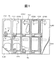
以下、本発明の実施の形態について、実施例の図面を参照して詳細に説明する。図1は本発明の液晶表示装置を構成する画素部の平面図であり、理解を容易にするため、各構成層の一部を破断し、あるいは除去して示す。また、図2〜図5はそれぞれ図1のA−A’線、B−B’線、C−C’線、D−D’線で切断した断面図である。なお、以下の実施例では、アクティブ素子として薄膜トランジスタを用いた例で説明する。各図中、参照符号SUB1は第1基板であるアクティブ・マトリクス基板、SUB2は第2基板(対向基板)、TFTは単位画素を駆動する薄膜トランジスタである。
【0016】
アクティブ・マトリクス基板SUB1の内面には、モノクロ表示の場合の1画素を構成する一つの単位画素、あるいはカラー表示の場合のカラー1画素を構成する赤(R)、緑(G)、青(B)の各単位画素は2本のデータ線(以下、ドレイン線)DLと2本の走査線(以下、ゲート線)GLで囲まれた領域(画素領域)に形成される。この単位画素をオン/オフ駆動する薄膜トランジスタTFTは画素領域の一郭に形成される。図2〜図4はアクティブ・マトリクス基板SUB1に薄膜トランジスタTFTおよび画素電極等を形成する工程を説明しており、図5はアクティブ・マトリクス基板SUB1に対向基板SUB2を貼り合わせ、内部に液晶層を封入した状態を示す。
【0017】
図2において、ゲート線GLの一部は薄膜トランジスタTFTのゲート電極となり、その上に第1の絶縁層IN1を介して半導体層SIが所要のパターンに形成され、この半導体層SI上にアルミニウム、クロム、モリブデン、その他の金属膜の成膜とパターニングでソース電極SD1およびドレイン電極SD2が形成される。そして、その上層には第2の絶縁層IN2が形成される。第2の絶縁層IN2にコンタクトホールTHを穿ち、このコンタクトホールTHを通してインジウム・チン・オキイドを好適とする導電層を蒸着等で成膜し、ソース電極SD1と電気的に接続された第1の電極層ITO1を画素領域毎にその大略全域にわたる範囲に形成する(図1参照)。
【0018】
そして、画素領域内の第1の電極層ITO1を覆って各色のカラーフィルタ層が塗布される。図3は図1のB−B’線の沿った断面を示す。この画素には緑(G)のカラーフィルタ層CF(G)が形成される。このとき、カラーフィルタ層の一部に開孔部CFHを設ける。開孔部CFH内には下層にある第1の電極層ITO1が見えている。
【0019】
次に、図4に示したように、カラーフィルタ層CFを覆って第2のデータ層ITO2を蒸着等で形成する。図4は青の蛍光体層CF(B)の単位画素の部分の断面図である。図示されたように、第2の電極層ITO2はカラーフィルタ層CFの開孔部CFHを通して第1の電極層ITO1と電気的に接続される。この第2の電極層ITO2は画素電極となる。その後、第2の電極層ITO2の上層に配向膜を形成してアクティブ・マトリクス基板が完成する。なお、配向膜は図示は省略した。
【0020】
図5は上記のようにして製造されたアクティブ・マトリクス基板に共通電極ITO3を有する対向基板である第2基板SUB2を液晶層CLを介して貼り合わせた状態を示す図1のD−D’線の沿った断面図である。
【0021】
本実施例の液晶表示装置では、アクティブ・マトリクス基板側に形成したカラーフィルタ層CFの上に画素電極である第2の電極層ITO2と対向基板SUB2に共通電極ITO3の間に形成される電界で液晶層CLの配向が制御され、所定の色の単位画素が駆動されて画像表示が行われる。カラーフィルタ層CFに設ける開孔部CFHの面積比をあまり大きくすると色相の劣化が目立つので、この大きさは1%〜20%とするのが望ましい。この面積比は液晶パネルのサイズや実装する電子機器の種類等、表示品質の要求性能を勘案して決めればよい。
【0022】
本実施例によれば、従来のように、金属層で形成されたソース電極SD1(あるいはドレイン電極SD2)と画素電極であるインジウム・チン・オキサイドで形成される透明電極ITOとを電気的に接続のためのコンタクト層の形成を要せず、従ってこのようなコンタクト層の形成のためのプロセスを必要としない。また、アクティブ・マトリクス基板SUB1は従来のカラーフィルタ分離型のアクティブ・マトリクス基板の製造プロセスをそのまま採用できるため、新規な製造設備を要しない。
【0023】
さらに、第1の電極層ITO1と第2の電極層ITO2の電気的接続部を画素領域の内部で行うため、画素領域の外側にはゲート線やドレイン線が存在するために、膜面が不整でかつコンタクトホールの大きさ、位置に制限がある。本実施例によれば、このような部分にコンタクトホールTHを形成しないため、第1の電極層ITO1と第2の電極層ITO2の電気的接続を容易に、かつ確実に行うことはでき、信頼性が向上する。
【0024】
そして、本実施例は、共に透明な第1の電極層ITO1と第2の電極層ITO2を直接接続するため、当該接続の信頼性が向上し、また、開口率の低下はなく、明るい画像表示を得ることができる。
【0025】
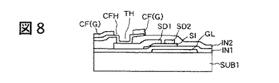
図6は本発明の第2実施例を説明する図1と同様の画素部の平面図である。また、図7〜図10は図6のA−A’線、B−B’線、C−C’線、D−D’線で切断した断面図である。本実施例は、図7に示したように、アクティブ・マトリクス基板SUB1上に薄膜トランジスタTFTを形成し、薄膜トランジスタTFTのソース電極SD1と接続する第1の電極層ITO1の形成までは第1実施例と同様であるので、繰り返しの説明は省略する。本実施例では、第1の電極層ITO1の上層に形成するカラーフィルタ層CFNI設ける開孔部CFHの位置を薄膜トランジスタTFTのソース電極SD1の直上で第1の電極層ITO1と当該ソース電極SD1との接続部分を含む部分としたものである。
【0026】
薄膜トランジスタTFTのソース電極SD1の部分は、画素領域でカラーフィルタ層の光透過に寄与しない部分である。したがって、ソース電極SD1を含んだ部分にカラーフィルタ層CFの開孔部CFHを設けることで当該開孔部CFHにより色相の劣化を低減できる。図7〜図10は、カラーフィルタ層CFの開孔部CFHの位置を除いては同様である。また、本実施例の他の効果は第1実施例と同様であるので繰り返しの説明は省略する。
【0027】
図11は本発明の第3実施例を説明する図1および図2と同様の画素部の平面図である。本実施例は、薄膜トランジスタTFTのソース電極SD1に接続する第1の電極層ITO1を当該ソース電極SD1の近傍のみに限定したものである。第1の電極層ITO1はカラーフィルタ層CFの上層に成膜する第2の電極層ITO2との電気的接続の機能を有するのみでよい。したがって、本実施例では、前記の各実施例のように画素領域の大略全域を覆って第1の電極層ITO1を形成せずに、必要な部分にのみ第1の電極層ITO1を形成した。
【0028】
カラーフィルタ層CFに設ける開孔部CFHは、この第1の電極層ITO1の位置に合わせて形成する。そして、カラーフィルタ層CFの上層に形成する画素電極となる第2の電極層ITO2は、図中に参照符号COTで示した部分で第1の電極層ITO1と電気的に接続される。
【0029】
本実施例によれば、第1の電極層ITO1を必要最小限の面積とすることで画素の透過率を向上できる。他の効果は前記の各実施例と同様であるので、繰り返しの説明は省略する。
【0030】
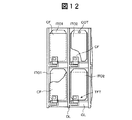
図12は本発明の第4実施例を説明する画素部の平面図である。本実施例では、例えば第1実施例における第1の電極層ITO1の上層に形成するカラーフィルタ層CFの一部を当該第1の電極層ITO1の端縁から後退させて塗布する。このカラーフィルタ層CFの上に第2の電極層ITO2を画素領域の大略全域に形成することで、上記カラーフィルタ層CFの後退で露呈した第1の電極層ITO1と電気的に接続される。この接続部分を参照符号COTで示す。本実施例の効果は第1の実施例と同様である。
【0031】
図13は本発明の第5実施例を説明する図12と同様の画素部の平面図である。本実施例では、例えば第1実施例における第1の電極層ITO1の上層に形成するカラーフィルタ層CFを第1の電極層ITO1の領域で分割し、カラーフィルタ層CFが露呈した露呈部を設けた。このカラーフィルタ層CFの上に第2の電極層ITO2を画素領域の大略全域に形成することで、上記カラーフィルタ層CFの分割で露呈した第1の電極層ITO1と画素領域内で電気的に接続される。この接続部分を参照符号COTで示す。なお、カラーフィルタ層CFの分割は図13に示したようにゲート線GLの延在方向と平行な方向に限るものではなく、ドレイン線DLと平行な方向、非平行な方向、あるいはそれらを組合せて分割数を3以上とすることも可能である。本実施例の効果は第1の実施例等と同様である。
【0032】
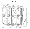
図14は本発明の第6実施例を説明する画素部の平面図であり、理解を容易にするため、各構成層の一部を破断し、あるいは除去して示す。また、図15〜図18はそれぞれ図14のA−A’線、B−B’線、C−C’線、D−D’線で切断した断面図である。本実施例は、例えば図1で説明した本発明の第1実施例にスペーサを設けたものである。通常、アクティブ・マトリクス基板SUB1と対向基板SUB2の間隙を所定値に保持するために、両者の間にスペーサを介挿している。本実施例では、このスペーサを、アクティブ・マトリクス基板SUB1に固定した、所謂柱状スペーサSPとしたものである。この柱状スペーサSPは第2の電極層ITO2の上、かつカラーフィルタ層CFに設けた開孔部CFHの直上に形成した。
【0033】
図15と図16までは前記実施例と同様のプロセスで各層が形成される。その後、図17に示したように、柱状スペーサSPをホトリソグラフィー技法などを用いてカラーフィルタ層CFの開孔部CFHに設ける。このとき、柱状スペーサSPを遮光性材料で形成すれば、開口率は低下するが、当該開孔部CFHからの光抜けを抑制してコントラストを向上することができる。なお、柱状スペーサに代えて粒状のスペーサ(スペーサビーズ)を設けてもよい。スペーサビーズはスプレーで散布されるが、このときに凹部を形成するカラーフィルタ層CFの開孔部CFHに当該スペーサビーズが配置される確率が大きくなる。スペーサビーズを用いる場合は、画素領域の内部にランダムに散布されるので、ガラスあるいはプラスチックの透明ビーズを用いるのが望ましい。
【0034】
図19は本発明の第7実施例を説明する画素部の平面図であり、理解を容易にするため、各構成層の一部を破断し、あるいは除去して示す。また、図20〜図23はそれぞれ図19のA−A’線、B−B’線、C−C’線、D−D’線で切断した断面図である。本実施例は、図6で説明した本発明の第2実施例に相当するアクティブ・マトリクス基板SUB1を用い、対向基板SUB2におけるカラーフィルタ層CFの開孔部CFHに対応した部分に遮光膜BSを設けたものである。
【0035】
すなわち、図20〜図22は図7〜図9と同様であり、図23に示した対向基板SUB2に遮光膜BSを設けた。この遮光膜BSは図19のカラーフィルタ層CFの開孔部CFHである第1の電極層ITO1と第2の電極層ITO2との接続部分の直上に位置する。遮光膜BSの大きさはカラーフィルタ層CFの開孔部CFHと同等とするのが望ましいが、それより多少の大きくても、あるいは小さくてもよい。
【0036】
本実施例によれば、画素の開口率は若干低下するが、開孔部CFHを透過する光Lを遮断することで色相低下を抑制し、コントラストの向上を図ることができ、高精細の画像表示装置に好適である。本実施例の他の効果は本発明の第2実施例と同様である。
【0037】
図24は本発明による液晶表示装置の全体構成の一例を説明する展開斜視図である。また、図25は図24のE−E’線に相当する位置で切断した断面図である。図24中、参照符号PNLは液晶パネルを示し、前記実施例において説明したアクティブ・マトリクスSUB1と対向基板SUB2の貼り合わせたものの表裏にそれぞれ偏光板(図示せず)を貼付して構成されている。また、この液晶パネルPNLの周縁には画素を構成する薄膜トランジスタに表示データや走査信号を供給するための駆動回路チップDICが搭載されている。
【0038】
また、参照符号OPSはプリズムシートや拡散シートからなる光学シート、GLBは導光板、RFSは反射シート、MDLはモールドフレーム、SHDはシルドフレーム、CFLは導光板GLBと共にバックライトを構成する冷陰極蛍光ランプ、RFSは反射板である。また、参照符号FPC1、FPC2は駆動回路チップDIC等に表示のためのデータやタイミング信号を供給するためのフレキシブルプリント基板、LPCはランプケーブルを示す。
【0039】
導光板GLBはモールドフレームMDLの内側に設置され、その下側には反射板RFSが設けられている。導光板GLBの液晶パネルPNL側にはプリズムシートや拡散シートからなる光学シートOPSが重ね合わされてモールドフレームMDLに収容されている。そして、導光板GLBのの両側の側縁に沿って冷陰極蛍光ランプCFLが配置されている。
【0040】
なお、図25には駆動回路チップDICやフレキシブルプリント基板FPC1、FPC2等は図示を省略してある。このような構成とした液晶表示装置において、液晶パネルPNLは導光板GLB、冷陰極蛍光ランプCFL、ランプ反射シートLFS等で構成されたバックライトからの光で照明され、当該液晶パネルPNLに形成された電子潜像を可視化する。
【0041】
図26は本発明の液晶表示装置を構成する液晶表示装置の回路構成を簡略に説明するブロック図である。図中、参照符号ARは液晶パネルの有効表示領域を示し、この有効表示領域ARにおいて前記した第1の基板SUB1の内面にゲート線(走査線)GL、ドレイン線(データ線)GL、共通電極線CL、薄膜トランジスタTFT、カラーフィルタ層CF、画素電極(ITO2)等が形成されている。走査線GLとデータ線GLの交差部分に画素選択用の薄膜トランジスタTFTが形成されている(図示せず)。共通電極線CLは前記した第1の基板(対向基板SUB2)の内面に形成された共通電極に共通電位を供給するものであり、、アクティブ・マトリクス基板SUB1側から端子Vcomを介して体好基板SUB2側に接続される。
【0042】
走査線GLは走査回路GDRで駆動され、データ線GLにはデータ線駆動回路DDRから表示データが供給される。コントローラCTLは外部信号源SSCから入力する表示信号に基づいて表示データやタイミング信号などの制御信号を生成する。表示データはデータ線駆動回路DDRに与えられ、制御信号は走査回路GDRに印加される。電源回路PWUは液晶表示装置に必要とれる各種の電圧を生成する。
【0043】
図27は本発明の液晶表示装置を適用した電子機器の一例であるテレビ受像機の外観図である。このテレビ受像機は表示部DSPとスタンド部STDで構成され、比較的大サイズの画面を有する液晶パネルPNLを有する液晶表示装置が表示部DSPに実装される。液晶表示装置の画面となる液晶パネルPNLの有効表示領域は表示部に露呈されている。このテレビ受像機の表示部に本発明の液晶表示装置を実装することで、高品質、高信頼性の画像表示装置を実現できる。
【0044】
なお、本発明は、上記実施例のサイドエッジ型バックライトを用いた液晶表示装置に限らず、液晶表示装置の背面に直接複数の冷陰極蛍光ランプを配置した、所謂直下型のバックライト、あるいはバックライトやフロントライト等の補助照明装置を備えた、あるいはこのような補助照明装置を備えない携帯電話機等の電子端末にも同様に適用できることは言うまでもない。
【0045】
【発明の効果】
以上説明したように、本発明によれば、従来のカラーフィルタ分離型のアクティブ・マトリクス基板の製造工程を変更することなくカラーフィルタ一体型アクティブ・マトリクス基板を用いた高品質の液晶表示装置を提供することができる。
【図面の簡単な説明】
【図1】本発明の液晶表示装置を構成する画素部の平面図である。
【図2】図1のA−A’線で切断した断面図である。
【図3】図1のB−B’線で切断した断面図である。
【図4】図1のC−C’線で切断した断面図である。
【図5】図1のD−D’線で切断した断面図である。
【図6】本発明の第2実施例を説明する図1と同様の画素部の平面図である。
【図7】図6のA−A’線で切断した断面図である。
【図8】図6のB−B’線で切断した断面図である。
【図9】図6のC−C’線で切断した断面図である。
【図10】図6のD−D’線で切断した断面図である。
【図11】本発明の第3実施例を説明する図1および図2と同様の画素部の平面図である。
【図12】本発明の第4実施例を説明する画素部の平面図である。
【図13】本発明の第5実施例を説明する画素部の平面図である。
【図14】本発明の第6実施例を説明する画素部の平面図である。
【図15】図14のA−A’線で切断した断面図である。
【図16】図14のB−B’線で切断した断面図である。
【図17】図14のC−C’線で切断した断面図である。
【図18】図14のD−D’線で切断した断面図である。
【図19】本発明の第7実施例を説明する画素部の平面図である。
【図20】図19のA−A’線で切断した断面図である。
【図21】図19のB−B’線で切断した断面図である。
【図22】図19のC−C’線で切断した断面図である。
【図23】図19のD−D’線で切断した断面図である。
【図24】本発明による液晶表示装置の全体構成の一例を説明する展開斜視図である。
【図25】図24のE−E’線に相当する位置で切断した断面図である。
【図26】本発明の液晶表示装置を構成する液晶表示装置の回路構成を簡略に説明するブロック図である。
【図27】本発明の液晶表示装置を適用した電子機器の一例であるテレビ受像機の外観図である。
【符号の説明】
SUB1・・・・第1基板(アクティブ・マトリクス基板)、DL・・・・データ線(ドレイン線)、GL・・・・走査線(ゲート線)、TFT・・・・薄膜トランジスタ、SUB2・・・・対向基板、IN1・・・・第1の絶縁層、IN2・・・・第2の絶縁層、SI・・・・半導体層、SD1・・・・ソース電極、SD2・・・・ドレイン電極、TH・・・・コンタクトホール、ITO1・・・・第1の電極層、ITO2・・・・第2の電極層、CF(CF(R),CF(G),CF(B))・・・・カラーフィルタ層、CFH・・・・開孔部、ITO3・・・・共通電極。[0001]
BACKGROUND OF THE INVENTION
The present invention relates to a liquid crystal display device, and more particularly to a liquid crystal display device having a color filter layer on a substrate side on which an active element is formed.
[0002]
[Prior art]
2. Description of the Related Art Active matrix type liquid crystal display devices are various as liquid crystal display devices capable of high-definition and color display for notebook computers, computer monitors, or television receivers. This type of liquid crystal display device basically has a so-called liquid crystal panel in which a liquid crystal layer is sandwiched between two substrates, at least one of which is made of a transparent substrate such as a glass plate. The liquid crystal panel has a driving circuit (driving IC) and wirings mounted or formed around it, and a liquid crystal display device is formed by combining a control circuit board and an auxiliary lighting device such as a backlight as necessary. . In the following description, even the description of the configuration of the liquid crystal panel itself will be described as a liquid crystal display device for convenience.
[0003]
One substrate (hereinafter referred to as a first substrate) of the liquid crystal display device has an active element such as a thin film transistor or a thin film diode and a pixel electrode driven by the active element, and the other substrate (hereinafter referred to as a second substrate). There is known a so-called vertical electric field type (TN type) liquid crystal display device in which a common electrode for forming an electric field for driving liquid crystal is formed between the pixel electrode and the pixel electrode. An example of an active matrix type liquid crystal display device of this type is disclosed in Japanese Patent Application Laid-Open No. 63-309921.
[0004]
On the other hand, a so-called lateral electric field type (IPS type) liquid crystal display device in which the common electrode is formed on the first substrate side and the direction of the electric field applied to the liquid crystal layer is substantially parallel to the substrate surface has been put into practical use. ing. Japanese Patent Publication No. 63-21907, which uses a comb electrode on one of two substrates to obtain a very wide viewing angle, can be cited as a disclosure of this IPS liquid crystal display device. .
[0005]
In each of the above-described liquid crystal display devices, three color filter layers are provided on the first substrate or the second substrate for full color display. The color filter layer provided on the second substrate side is widely known, but there is a method of forming the color filter layer on the first substrate side. In either method, color display is obtained by color-modulating light passing through a liquid crystal layer between a pixel electrode selected by an active element and a common electrode with a color filter layer.
[0006]
In general, the first substrate is also referred to as an active matrix substrate because it has active elements such as thin film transistors for driving pixels in a matrix. In the following description, it is assumed that the first substrate is an active matrix substrate and the active elements are thin film transistors. The method of forming the color filter layer on the active matrix substrate has an advantage that the overlaying process with the second substrate that is opposed and superimposed is easy. Hereinafter, the second substrate is also referred to as a counter substrate.
[0007]
[Problems to be solved by the invention]
In the active matrix substrate, a large number of thin film transistors are formed in a matrix on the substrate, and a first electrode layer is formed on a drive terminal (output terminal) of the thin film transistor. In the method having a color filter on the counter substrate side, the first electrode layer is a pixel electrode. However, in the liquid crystal display device of the present invention, a color filter layer is formed to cover the first electrode layer, A second electrode layer formed as a separate member from the first electrode layer is provided above the color filter layer, and is electrically connected to the first electrode layer to form a pixel electrode.
[0008]
In the examples described later, the common electrodes provided on the first electrode layer, the second electrode layer, and the counter substrate are all assumed to be ITO (indium tin oxide), but in addition to this, IZO (indium. Zinc oxide) and other transparent conductive films can be used. An area where each thin film transistor is arranged is a pixel area, and a color filter layer is applied to the pixel area. Then, a second electrode layer serving as a pixel electrode is formed so as to cover the color filter layer. At this time, it is necessary to electrically connect the second electrode layer to the first electrode layer.
[0009]
In a conventional liquid crystal display device employing this type of color filter integrated active matrix substrate, a contact hole is formed in the driving output portion of the thin film transistor after the color filter layer is formed, and is provided in the upper layer of the color filter layer through this contact hole. The electrode layer (pixel electrode) and the drive output portion of the thin film transistor are electrically connected. In some cases, the electrical connection between the first substrate and the second substrate is performed in a portion that avoids the pixel region. For this reason, there are many cases where the film surface is irregular because there are wirings for applying various signals for the purpose. For this reason, there is a limit to increasing the connection reliability between the electrode layer (pixel electrode) and the drive output portion of the thin film transistor. Also, conventionally, it is necessary to employ a specific manufacturing process such as a step of forming a contact hole after forming a color filter, etc., such as an increase in photolithography processes, and so-called forming a color filter on the counter substrate side. There is a problem that the number of manufacturing steps is increased as compared with the case of the color filter separation type, and this is one of the problems to be solved.
[0010]
An object of the present invention is to solve the above-described problems in the prior art and obtain a low-cost and high-reliability liquid crystal display device without changing the manufacturing process of a conventional color filter separation type active matrix substrate. An active matrix substrate integrated with a color filter can be obtained.
[0011]
[Means for Solving the Problems]
In order to achieve the above object, the present invention provides a first electrode layer comprising a conductive thin film electrically connected to a drive output terminal of an active element in each of pixel regions of a first substrate which is an active matrix substrate. And a color filter layer having an opening formed in a part of the color filter layer in each pixel region or an exposed part with an edge exposing a part of the first electrode layer. By covering the color filter layer and forming a second electrode layer to be a pixel electrode, the second electrode layer is electrically connected to the first electrode layer through the aperture or the exposed portion. The first electrode layer has a structure equivalent to that of the above-described conventional color filter separation type active matrix substrate, and the color filter separation type serves as a pixel electrode.
[0012]
Therefore, the conventional color filter separation type active matrix substrate manufacturing process can be used as it is up to the pre-process of forming the color filter layer, the alignment with the counter substrate is easy, the throughput is improved, and the cost is reduced. Is possible. In addition, since the electrical connection portion between the first electrode layer and the second electrode layer is in the pixel region, both electrode layers are connected with high accuracy, and reliability is improved.
[0013]
Furthermore, light leakage is suppressed by providing a spacer for regulating the gap between the active matrix substrate and the counter substrate in the electrical connection portion. Furthermore, by providing a light-shielding layer in the aperture portion of the color filter layer or the portion of the counter substrate corresponding to the exposed portion, the aperture ratio is reduced, but the contrast can be improved.
[0014]
It should be noted that the present invention is not limited to the above-described configuration and the configuration of the embodiments described later, and it goes without saying that various modifications can be made without departing from the technical idea of the present invention.
[0015]
DETAILED DESCRIPTION OF THE INVENTION
Embodiments of the present invention will be described below in detail with reference to the drawings of the embodiments. FIG. 1 is a plan view of a pixel portion constituting the liquid crystal display device of the present invention. For easy understanding, a part of each constituent layer is broken or removed. 2 to 5 are cross-sectional views taken along lines AA ′, BB ′, CC ′, and DD ′ of FIG. 1, respectively. In the following embodiments, an example in which a thin film transistor is used as an active element will be described. In each figure, reference numeral SUB1 is an active matrix substrate that is a first substrate, SUB2 is a second substrate (counter substrate), and TFT is a thin film transistor that drives a unit pixel.
[0016]
On the inner surface of the active matrix substrate SUB1, red (R), green (G), blue (B) constituting one unit pixel constituting one pixel for monochrome display or one color pixel for color display is provided. ) Is formed in an area (pixel area) surrounded by two data lines (hereinafter, drain lines) DL and two scanning lines (hereinafter, gate lines) GL. The thin film transistor TFT for driving the unit pixel on / off is formed in the pixel area. 2 to 4 illustrate a process of forming a thin film transistor TFT, a pixel electrode, and the like on the active matrix substrate SUB1, and FIG. 5 attaches a counter substrate SUB2 to the active matrix substrate SUB1 and encloses a liquid crystal layer therein. Shows the state.
[0017]
In FIG. 2, a part of the gate line GL becomes a gate electrode of the thin film transistor TFT, and a semiconductor layer SI is formed in a required pattern via the first insulating layer IN1, and aluminum, chromium are formed on the semiconductor layer SI. The source electrode SD1 and the drain electrode SD2 are formed by depositing and patterning molybdenum, other metal films. A second insulating layer IN2 is formed on the upper layer. A contact hole TH is formed in the second insulating layer IN2, and a conductive layer suitable for indium, chin, and oxide is formed by vapor deposition or the like through the contact hole TH, and is electrically connected to the source electrode SD1. The electrode layer ITO1 is formed in a range covering almost the entire region for each pixel region (see FIG. 1).
[0018]
Then, a color filter layer of each color is applied so as to cover the first electrode layer ITO1 in the pixel region. FIG. 3 shows a cross section taken along line BB ′ of FIG. In this pixel, a green (G) color filter layer CF (G) is formed. At this time, the opening CFH is provided in a part of the color filter layer. The first electrode layer ITO1 in the lower layer is visible in the opening portion CFH.
[0019]
Next, as shown in FIG. 4, a second data layer ITO2 is formed by vapor deposition or the like so as to cover the color filter layer CF. FIG. 4 is a cross-sectional view of the unit pixel portion of the blue phosphor layer CF (B). As illustrated, the second electrode layer ITO2 is electrically connected to the first electrode layer ITO1 through the opening portion CFH of the color filter layer CF. The second electrode layer ITO2 becomes a pixel electrode. Thereafter, an alignment film is formed on the second electrode layer ITO2 to complete the active matrix substrate. The alignment film is not shown.
[0020]
FIG. 5 is a DD ′ line in FIG. 1 showing a state in which the second substrate SUB2, which is a counter substrate having the common electrode ITO3, is bonded to the active matrix substrate manufactured as described above via the liquid crystal layer CL. FIG.
[0021]
In the liquid crystal display device of this embodiment, an electric field formed between the second electrode layer ITO2 as a pixel electrode and the common electrode ITO3 on the counter substrate SUB2 on the color filter layer CF formed on the active matrix substrate side. The orientation of the liquid crystal layer CL is controlled, and unit pixels of a predetermined color are driven to perform image display. If the area ratio of the opening portion CFH provided in the color filter layer CF is too large, the hue is noticeably deteriorated. Therefore, the size is desirably 1% to 20%. This area ratio may be determined in consideration of the required performance of display quality such as the size of the liquid crystal panel and the type of electronic device to be mounted.
[0022]
According to this embodiment, the source electrode SD1 (or the drain electrode SD2) formed of a metal layer and the transparent electrode ITO formed of indium tin oxide, which is a pixel electrode, are electrically connected as in the past. Therefore, it is not necessary to form a contact layer, and thus a process for forming such a contact layer is not required. In addition, since the active matrix substrate SUB1 can employ the manufacturing process of the conventional color filter separation type active matrix substrate as it is, no new manufacturing equipment is required.
[0023]
Furthermore, since the electrical connection between the first electrode layer ITO1 and the second electrode layer ITO2 is performed inside the pixel region, the gate line and the drain line exist outside the pixel region, so that the film surface is irregular. In addition, the size and position of the contact hole are limited. According to the present embodiment, since the contact hole TH is not formed in such a portion, the electrical connection between the first electrode layer ITO1 and the second electrode layer ITO2 can be easily and reliably performed. Improves.
[0024]
In this embodiment, since the first electrode layer ITO1 and the second electrode layer ITO2 which are both transparent are directly connected, the reliability of the connection is improved, and the aperture ratio is not lowered and a bright image display is achieved. Can be obtained.
[0025]
FIG. 6 is a plan view of a pixel portion similar to FIG. 1 for explaining the second embodiment of the present invention. 7 to 10 are cross-sectional views taken along lines AA ′, BB ′, CC ′, and DD ′ of FIG. In this embodiment, as shown in FIG. 7, the thin film transistor TFT is formed on the active matrix substrate SUB1, and the formation of the first electrode layer ITO1 connected to the source electrode SD1 of the thin film transistor TFT is the same as that of the first embodiment. Since it is the same, repeated description is omitted. In the present embodiment, the position of the opening portion CFH provided in the color filter layer CFNI formed on the first electrode layer ITO1 is positioned immediately above the source electrode SD1 of the thin film transistor TFT between the first electrode layer ITO1 and the source electrode SD1. It is a part including a connection part.
[0026]
The portion of the source electrode SD1 of the thin film transistor TFT is a portion that does not contribute to light transmission of the color filter layer in the pixel region. Therefore, by providing the opening portion CFH of the color filter layer CF in the portion including the source electrode SD1, the deterioration of the hue can be reduced by the opening portion CFH. 7 to 10 are the same except for the position of the opening portion CFH of the color filter layer CF. Further, since the other effects of the present embodiment are the same as those of the first embodiment, repeated description is omitted.
[0027]
FIG. 11 is a plan view of a pixel portion similar to FIGS. 1 and 2 for explaining a third embodiment of the present invention. In this embodiment, the first electrode layer ITO1 connected to the source electrode SD1 of the thin film transistor TFT is limited to the vicinity of the source electrode SD1. The first electrode layer ITO1 only needs to have a function of electrical connection with the second electrode layer ITO2 formed on the color filter layer CF. Therefore, in the present embodiment, the first electrode layer ITO1 is formed only in a necessary portion without forming the first electrode layer ITO1 so as to cover almost the entire pixel region as in the above embodiments.
[0028]
The opening portion CFH provided in the color filter layer CF is formed in accordance with the position of the first electrode layer ITO1. The second electrode layer ITO2, which is a pixel electrode formed on the color filter layer CF, is electrically connected to the first electrode layer ITO1 at a portion indicated by reference numeral COT in the drawing.
[0029]
According to the present embodiment, the transmittance of the pixel can be improved by setting the first electrode layer ITO1 to the necessary minimum area. Since other effects are the same as those of the above-described embodiments, repeated description is omitted.
[0030]
FIG. 12 is a plan view of a pixel portion for explaining a fourth embodiment of the present invention. In the present embodiment, for example, a part of the color filter layer CF formed on the upper layer of the first electrode layer ITO1 in the first embodiment is applied so as to recede from the edge of the first electrode layer ITO1. By forming the second electrode layer ITO2 on the color filter layer CF over almost the entire pixel region, the second electrode layer ITO2 is electrically connected to the first electrode layer ITO1 exposed by the retreat of the color filter layer CF. This connecting portion is indicated by reference numeral COT. The effect of this embodiment is the same as that of the first embodiment.
[0031]
FIG. 13 is a plan view of a pixel portion similar to FIG. 12 for explaining the fifth embodiment of the present invention. In the present embodiment, for example, the color filter layer CF formed on the upper layer of the first electrode layer ITO1 in the first embodiment is divided by the region of the first electrode layer ITO1, and an exposed portion where the color filter layer CF is exposed is provided. It was. By forming the second electrode layer ITO2 on the color filter layer CF over almost the entire pixel region, the first electrode layer ITO1 exposed by the division of the color filter layer CF and the pixel region are electrically connected. Connected. This connecting portion is indicated by reference numeral COT. The division of the color filter layer CF is not limited to the direction parallel to the extending direction of the gate line GL as shown in FIG. 13, but the direction parallel to the drain line DL, the non-parallel direction, or a combination thereof. Thus, the number of divisions can be 3 or more. The effect of this embodiment is the same as that of the first embodiment.
[0032]
FIG. 14 is a plan view of a pixel portion for explaining the sixth embodiment of the present invention. For easy understanding, a part of each constituent layer is broken or removed. 15 to 18 are cross-sectional views taken along lines AA ′, BB ′, CC ′, and DD ′ of FIG. 14, respectively. In this embodiment, for example, a spacer is provided in the first embodiment of the present invention described in FIG. Usually, in order to keep the gap between the active matrix substrate SUB1 and the counter substrate SUB2 at a predetermined value, a spacer is interposed between them. In this embodiment, the spacer is a so-called columnar spacer SP fixed to the active matrix substrate SUB1. This columnar spacer SP was formed on the second electrode layer ITO2 and immediately above the aperture CFH provided in the color filter layer CF.
[0033]
15 and 16, each layer is formed by the same process as in the above embodiment. Thereafter, as shown in FIG. 17, columnar spacers SP are provided in the apertures CFH of the color filter layer CF by using a photolithography technique or the like. At this time, if the columnar spacers SP are formed of a light-shielding material, the aperture ratio is reduced, but light leakage from the apertures CFH can be suppressed and the contrast can be improved. Note that granular spacers (spacer beads) may be provided instead of the columnar spacers. The spacer beads are dispersed by spraying, and at this time, the probability that the spacer beads are arranged in the opening portion CFH of the color filter layer CF that forms the concave portion is increased. When spacer beads are used, glass or plastic transparent beads are preferably used because they are randomly distributed inside the pixel region.
[0034]
FIG. 19 is a plan view of a pixel portion for explaining a seventh embodiment of the present invention. For easy understanding, a part of each constituent layer is broken or removed. 20 to 23 are cross-sectional views taken along lines AA ′, BB ′, CC ′, and DD ′ of FIG. 19, respectively. In this embodiment, the active matrix substrate SUB1 corresponding to the second embodiment of the present invention described with reference to FIG. 6 is used, and a light shielding film BS is formed in a portion corresponding to the opening portion CFH of the color filter layer CF in the counter substrate SUB2. It is provided.
[0035]
That is, FIGS. 20 to 22 are the same as FIGS. 7 to 9, and the light shielding film BS is provided on the counter substrate SUB2 shown in FIG. This light-shielding film BS is located immediately above the connection portion between the first electrode layer ITO1 and the second electrode layer ITO2, which is the opening portion CFH of the color filter layer CF in FIG. The size of the light-shielding film BS is preferably equal to the opening portion CFH of the color filter layer CF, but may be slightly larger or smaller than that.
[0036]
According to the present embodiment, although the aperture ratio of the pixel is slightly reduced, the hue L can be suppressed by blocking the light L transmitted through the aperture portion CFH, the contrast can be improved, and a high-definition image can be obtained. Suitable for display devices. Other effects of this embodiment are the same as those of the second embodiment of the present invention.
[0037]
FIG. 24 is a developed perspective view for explaining an example of the entire configuration of the liquid crystal display device according to the present invention. FIG. 25 is a cross-sectional view taken along the line EE ′ of FIG. In FIG. 24, reference numeral PNL indicates a liquid crystal panel, which is configured by attaching polarizing plates (not shown) to the front and back of the bonded active matrix SUB1 and counter substrate SUB2 described in the above embodiment. . A driving circuit chip DIC for supplying display data and scanning signals to the thin film transistors constituting the pixels is mounted on the periphery of the liquid crystal panel PNL.
[0038]
Reference symbol OPS is an optical sheet composed of a prism sheet or a diffusion sheet, GLB is a light guide plate, RFS is a reflection sheet, MDL is a mold frame, SHD is a sill frame, and CFL is a cold cathode fluorescent light that forms a backlight together with the light guide plate GLB. The lamp and RFS are reflectors. Reference numerals FPC1 and FPC2 denote flexible printed boards for supplying display data and timing signals to the drive circuit chip DIC and the like, and LPC denotes a lamp cable.
[0039]
The light guide plate GLB is installed inside the mold frame MDL, and a reflection plate RFS is provided below the light guide plate GLB. An optical sheet OPS made of a prism sheet or a diffusion sheet is superposed on the liquid crystal panel PNL side of the light guide plate GLB and accommodated in the mold frame MDL. And the cold cathode fluorescent lamp CFL is arrange | positioned along the side edge of the both sides of the light-guide plate GLB.
[0040]
In FIG. 25, the drive circuit chip DIC, the flexible printed circuit boards FPC1, FPC2, and the like are not shown. In the liquid crystal display device having such a configuration, the liquid crystal panel PNL is illuminated with light from a backlight composed of a light guide plate GLB, a cold cathode fluorescent lamp CFL, a lamp reflecting sheet LFS, and the like, and is formed on the liquid crystal panel PNL. Visualize the electronic latent image.
[0041]
FIG. 26 is a block diagram for briefly explaining the circuit configuration of the liquid crystal display device constituting the liquid crystal display device of the present invention. In the drawing, reference symbol AR indicates an effective display area of the liquid crystal panel. In the effective display area AR, the gate line (scanning line) GL, the drain line (data line) GL, and the common electrode are formed on the inner surface of the first substrate SUB1. A line CL, a thin film transistor TFT, a color filter layer CF, a pixel electrode (ITO2), and the like are formed. A pixel selecting thin film transistor TFT is formed at the intersection of the scanning line GL and the data line GL (not shown). The common electrode line CL supplies a common potential to the common electrode formed on the inner surface of the first substrate (counter substrate SUB2). The body substrate is connected to the active matrix substrate SUB1 via the terminal Vcom. Connected to the SUB2 side.
[0042]
The scanning line GL is driven by the scanning circuit GDR, and display data is supplied to the data line GL from the data line driving circuit DDR. The controller CTL generates control signals such as display data and timing signals based on display signals input from the external signal source SSC. Display data is supplied to the data line driving circuit DDR, and a control signal is applied to the scanning circuit GDR. The power supply circuit PWU generates various voltages required for the liquid crystal display device.
[0043]
FIG. 27 is an external view of a television receiver which is an example of an electronic apparatus to which the liquid crystal display device of the present invention is applied. This television receiver includes a display unit DSP and a stand unit STD, and a liquid crystal display device having a liquid crystal panel PNL having a relatively large screen is mounted on the display unit DSP. The effective display area of the liquid crystal panel PNL serving as the screen of the liquid crystal display device is exposed on the display unit. By mounting the liquid crystal display device of the present invention on the display portion of the television receiver, a high-quality and highly reliable image display device can be realized.
[0044]
The present invention is not limited to the liquid crystal display device using the side edge type backlight of the above embodiment, but a so-called direct type backlight in which a plurality of cold cathode fluorescent lamps are arranged directly on the back surface of the liquid crystal display device, or Needless to say, the present invention can be similarly applied to an electronic terminal such as a mobile phone provided with an auxiliary illumination device such as a backlight or a front light or not provided with such an auxiliary illumination device.
[0045]
【The invention's effect】
As described above, according to the present invention, a high-quality liquid crystal display device using a color filter integrated active matrix substrate is provided without changing the manufacturing process of a conventional color filter separation type active matrix substrate. can do.
[Brief description of the drawings]
FIG. 1 is a plan view of a pixel portion constituting a liquid crystal display device of the present invention.
FIG. 2 is a cross-sectional view taken along the line AA ′ of FIG.
FIG. 3 is a cross-sectional view taken along line BB ′ of FIG.
4 is a cross-sectional view taken along line CC ′ of FIG. 1. FIG.
FIG. 5 is a cross-sectional view taken along the line DD ′ of FIG.
FIG. 6 is a plan view of a pixel portion similar to FIG. 1 for explaining a second embodiment of the present invention.
7 is a cross-sectional view taken along line AA ′ of FIG.
8 is a cross-sectional view taken along line BB ′ of FIG.
9 is a cross-sectional view taken along the line CC ′ of FIG.
10 is a cross-sectional view taken along the line DD ′ of FIG.
11 is a plan view of a pixel portion similar to FIGS. 1 and 2 for explaining a third embodiment of the present invention. FIG.
FIG. 12 is a plan view of a pixel portion for explaining a fourth embodiment of the present invention.
FIG. 13 is a plan view of a pixel portion for explaining a fifth embodiment of the present invention.
FIG. 14 is a plan view of a pixel portion for explaining a sixth embodiment of the present invention.
15 is a cross-sectional view taken along line AA ′ of FIG.
16 is a cross-sectional view taken along line BB ′ of FIG.
17 is a cross-sectional view taken along the line CC ′ of FIG.
18 is a cross-sectional view taken along the line DD ′ of FIG.
FIG. 19 is a plan view of a pixel portion for explaining a seventh embodiment of the present invention.
20 is a cross-sectional view taken along line AA ′ of FIG.
FIG. 21 is a cross-sectional view taken along line BB ′ of FIG.
22 is a cross-sectional view taken along the line CC ′ of FIG.
23 is a cross-sectional view taken along the line DD ′ of FIG.
FIG. 24 is a developed perspective view illustrating an example of the overall configuration of the liquid crystal display device according to the present invention.
25 is a cross-sectional view cut at a position corresponding to the line EE ′ of FIG. 24. FIG.
FIG. 26 is a block diagram for briefly explaining a circuit configuration of a liquid crystal display device included in the liquid crystal display device of the present invention.
FIG. 27 is an external view of a television receiver which is an example of an electronic apparatus to which the liquid crystal display device of the present invention is applied.
[Explanation of symbols]
SUB1... First substrate (active matrix substrate), DL... Data line (drain line), GL... Scanning line (gate line), TFT. .. Counter substrate, IN1... First insulating layer, IN2... Second insulating layer, SI... Semiconductor layer, SD1... Source electrode, SD2. TH ... contact hole, ITO1 ... first electrode layer, ITO2 ... second electrode layer, CF (CF (R), CF (G), CF (B)) ... · Color filter layer, CFH ··· opening, ITO3 ··· common electrode.
Claims (9)
前記第1基板の前記画素領域の夫々には、前記アクティブ素子の駆動出力端子に電気的に接続した導電性薄膜からなる第1の電極層が設けられ、
前記画素領域内の夫々にて前記カラーフィルタ層の一部に形成した当該カラーフィルタ層の開孔部と、
前記カラーフィルタ層の上層にて前記画素電極を形成し、且つ前記第1の電極層と前記開孔部を通して電気的に接続される第2の電極層とが設けられ、
前記第1の電極層と、前記第2の電極層は、透明電極であり、
前記アクティブ素子の前記駆動出力端子は、遮光性の金属膜であり、
前記第1基板は、複数の走査線と、前記複数の走査線に交差する複数のデータ線とを有し、
前記開孔部は、前記アクティブ素子の前記駆動出力端子が形成された第1の領域と、前記第1の領域以外の領域であって、かつ、前記走査線と前記データ線の何れとも重畳しない第2の領域との両方を含むように設けられていることを特徴とする液晶表示装置。A common electrode for forming an electric field is formed between a pixel electrode and a first substrate in which a plurality of pixel regions each including an active element and a color filter layer corresponding to the pixel electrode are arranged in a matrix, and the pixel electrode A liquid crystal display device comprising a liquid crystal panel having the second substrate and a liquid crystal layer sandwiched between the first substrate and the second substrate,
Each of the pixel regions of the first substrate is provided with a first electrode layer made of a conductive thin film electrically connected to a drive output terminal of the active element,
An opening portion of the color filter layer formed in a part of the color filter layer in each of the pixel regions;
The pixel electrode is formed in an upper layer of the color filter layer, and the second electrode layer electrically connected through the first electrode layer and the opening is provided.
The first electrode layer and the second electrode layer are transparent electrodes,
The drive output terminal of the active element is a light-shielding metal film,
The first substrate has a plurality of scanning lines and a plurality of data lines intersecting the plurality of scanning lines,
The aperture is a first region where the drive output terminal of the active element is formed and a region other than the first region, and does not overlap any of the scanning line and the data line. A liquid crystal display device including both the second region and the liquid crystal display device.
前記画素領域を前記走査線に平行な仮想的な線で第3の領域と第4の領域とに二等分したとき、前記アクティブ素子の前記駆動出力端子と前記開孔部は、ともに前記第3の領域内に配置されていることを特徴とする請求項1から4の何れかに記載の液晶表示装置。The pixel region is a region surrounded by a pair of adjacent scanning lines and a pair of adjacent data lines,
When the pixel region is equally divided into a third region and a fourth region by a virtual line parallel to the scanning line, both the drive output terminal and the aperture of the active element are the liquid crystal display device according to are arranged in three in the region from claim 1, wherein the one of the four.
前記第1基板の前記画素領域の夫々には、前記アクティブ素子の駆動出力端子に電気的に接続した導電性薄膜からなる第1の電極層が設けられ、
前記画素領域内の夫々にて前記カラーフィルタ層の一部に形成した当該カラーフィルタ層の開孔部と、
前記カラーフィルタ層の上層にて前記画素電極を形成し、且つ前記第1の電極層と前記開孔部を通して電気的に接続される第2の電極層とが設けられ、
前記第1基板は、複数の走査線と、前記複数の走査線に交差する複数のデータ線とを有し、
前記開孔部は、前記アクティブ素子の前記駆動出力端子が形成された第1の領域と、前記第1の領域以外の領域であって、かつ、前記走査線と前記データ線の何れとも重畳しない第2の領域との両方を含むように設けられ、
前記第1の電極層は、前記走査線の延在方向に長手方向を有し、
前記開孔部は、前記走査線の延在方向に長手方向を有し、
前記第1の電極層と、前記第2の電極層は、透明電極であり、
前記第1の電極層の面積は、前記第2の電極層の面積よりも小さく、
前記アクティブ素子の前記駆動出力端子は、遮光性の金属膜であることを特徴とする液晶表示装置。A common electrode for forming an electric field is formed between a pixel electrode and a first substrate in which a plurality of pixel regions each including an active element and a color filter layer corresponding to the pixel electrode are arranged in a matrix, and the pixel electrode A liquid crystal display device comprising a liquid crystal panel having the second substrate and a liquid crystal layer sandwiched between the first substrate and the second substrate,
Each of the pixel regions of the first substrate is provided with a first electrode layer made of a conductive thin film electrically connected to a drive output terminal of the active element,
An opening portion of the color filter layer formed in a part of the color filter layer in each of the pixel regions;
The pixel electrode is formed in an upper layer of the color filter layer, and the second electrode layer electrically connected through the first electrode layer and the opening is provided.
The first substrate has a plurality of scanning lines and a plurality of data lines intersecting the plurality of scanning lines,
The aperture is a first region where the drive output terminal of the active element is formed and a region other than the first region, and does not overlap any of the scanning line and the data line. Provided to include both the second region,
The first electrode layer has a longitudinal direction in the extending direction of the scanning line,
The aperture has a longitudinal direction in the extending direction of the scanning line,
The first electrode layer and the second electrode layer are transparent electrodes,
The area of the first electrode layer is smaller than the area of the second electrode layer,
The liquid crystal display device, wherein the drive output terminal of the active element is a light-shielding metal film.
前記画素領域を前記走査線に平行な仮想的な線で第3の領域と第4の領域とに二等分したとき、前記アクティブ素子の前記駆動出力端子と前記開孔部は、ともに前記第3の領域内に配置されていることを特徴とする請求項7に記載の液晶表示装置。The pixel region is a region surrounded by a pair of adjacent scanning lines and a pair of adjacent data lines,
When the pixel region is equally divided into a third region and a fourth region by a virtual line parallel to the scanning line, both the drive output terminal and the aperture of the active element are The liquid crystal display device according to claim 7 , wherein the liquid crystal display device is disposed in a region 3.
Priority Applications (2)
| Application Number | Priority Date | Filing Date | Title |
|---|---|---|---|
| JP2002205768A JP4170033B2 (en) | 2002-07-15 | 2002-07-15 | Liquid crystal display |
| US10/617,755 US6992738B2 (en) | 2002-07-15 | 2003-07-14 | Liquid crystal display device including an electrode constituting pixel electrode connected to another electrode through opening formed in color filter |
Applications Claiming Priority (1)
| Application Number | Priority Date | Filing Date | Title |
|---|---|---|---|
| JP2002205768A JP4170033B2 (en) | 2002-07-15 | 2002-07-15 | Liquid crystal display |
Publications (3)
| Publication Number | Publication Date |
|---|---|
| JP2004045970A JP2004045970A (en) | 2004-02-12 |
| JP2004045970A5 JP2004045970A5 (en) | 2005-08-18 |
| JP4170033B2 true JP4170033B2 (en) | 2008-10-22 |
Family
ID=31710983
Family Applications (1)
| Application Number | Title | Priority Date | Filing Date |
|---|---|---|---|
| JP2002205768A Expired - Fee Related JP4170033B2 (en) | 2002-07-15 | 2002-07-15 | Liquid crystal display |
Country Status (2)
| Country | Link |
|---|---|
| US (1) | US6992738B2 (en) |
| JP (1) | JP4170033B2 (en) |
Families Citing this family (34)
| Publication number | Priority date | Publication date | Assignee | Title |
|---|---|---|---|---|
| JP2005316404A (en) * | 2004-03-31 | 2005-11-10 | Seiko Epson Corp | Electro-optical device and electronic apparatus |
| US20070077218A1 (en) * | 2005-08-26 | 2007-04-05 | L'oreal | Composition containing a coloring agent |
| JP2007163620A (en) * | 2005-12-12 | 2007-06-28 | Hitachi Displays Ltd | Liquid crystal display device and backlight device |
| US7615706B2 (en) * | 2006-08-21 | 2009-11-10 | Tpo Displays Corp. | Layout of a printed circuit board |
| KR101304410B1 (en) * | 2006-09-19 | 2013-09-05 | 삼성디스플레이 주식회사 | Liquid crystal display device |
| TWI401495B (en) * | 2009-06-24 | 2013-07-11 | Au Optronics Corp | Display panel |
| US9223138B2 (en) | 2011-12-23 | 2015-12-29 | Microsoft Technology Licensing, Llc | Pixel opacity for augmented reality |
| US9606586B2 (en) | 2012-01-23 | 2017-03-28 | Microsoft Technology Licensing, Llc | Heat transfer device |
| US9779643B2 (en) | 2012-02-15 | 2017-10-03 | Microsoft Technology Licensing, Llc | Imaging structure emitter configurations |
| US9297996B2 (en) | 2012-02-15 | 2016-03-29 | Microsoft Technology Licensing, Llc | Laser illumination scanning |
| US9368546B2 (en) | 2012-02-15 | 2016-06-14 | Microsoft Technology Licensing, Llc | Imaging structure with embedded light sources |
| US9726887B2 (en) | 2012-02-15 | 2017-08-08 | Microsoft Technology Licensing, Llc | Imaging structure color conversion |
| US9578318B2 (en) | 2012-03-14 | 2017-02-21 | Microsoft Technology Licensing, Llc | Imaging structure emitter calibration |
| US11068049B2 (en) | 2012-03-23 | 2021-07-20 | Microsoft Technology Licensing, Llc | Light guide display and field of view |
| US9558590B2 (en) | 2012-03-28 | 2017-01-31 | Microsoft Technology Licensing, Llc | Augmented reality light guide display |
| US10191515B2 (en) | 2012-03-28 | 2019-01-29 | Microsoft Technology Licensing, Llc | Mobile device light guide display |
| US9717981B2 (en) | 2012-04-05 | 2017-08-01 | Microsoft Technology Licensing, Llc | Augmented reality and physical games |
| US10502876B2 (en) | 2012-05-22 | 2019-12-10 | Microsoft Technology Licensing, Llc | Waveguide optics focus elements |
| US8989535B2 (en) | 2012-06-04 | 2015-03-24 | Microsoft Technology Licensing, Llc | Multiple waveguide imaging structure |
| US9151984B2 (en) * | 2012-06-18 | 2015-10-06 | Microsoft Technology Licensing, Llc | Active reflective surfaces |
| US10192358B2 (en) | 2012-12-20 | 2019-01-29 | Microsoft Technology Licensing, Llc | Auto-stereoscopic augmented reality display |
| US9304235B2 (en) | 2014-07-30 | 2016-04-05 | Microsoft Technology Licensing, Llc | Microfabrication |
| US10678412B2 (en) | 2014-07-31 | 2020-06-09 | Microsoft Technology Licensing, Llc | Dynamic joint dividers for application windows |
| US10592080B2 (en) | 2014-07-31 | 2020-03-17 | Microsoft Technology Licensing, Llc | Assisted presentation of application windows |
| US10254942B2 (en) | 2014-07-31 | 2019-04-09 | Microsoft Technology Licensing, Llc | Adaptive sizing and positioning of application windows |
| US10018844B2 (en) | 2015-02-09 | 2018-07-10 | Microsoft Technology Licensing, Llc | Wearable image display system |
| US9827209B2 (en) | 2015-02-09 | 2017-11-28 | Microsoft Technology Licensing, Llc | Display system |
| US9429692B1 (en) | 2015-02-09 | 2016-08-30 | Microsoft Technology Licensing, Llc | Optical components |
| US9423360B1 (en) | 2015-02-09 | 2016-08-23 | Microsoft Technology Licensing, Llc | Optical components |
| US9535253B2 (en) | 2015-02-09 | 2017-01-03 | Microsoft Technology Licensing, Llc | Display system |
| US11086216B2 (en) | 2015-02-09 | 2021-08-10 | Microsoft Technology Licensing, Llc | Generating electronic components |
| US10317677B2 (en) | 2015-02-09 | 2019-06-11 | Microsoft Technology Licensing, Llc | Display system |
| US9513480B2 (en) | 2015-02-09 | 2016-12-06 | Microsoft Technology Licensing, Llc | Waveguide |
| US9372347B1 (en) | 2015-02-09 | 2016-06-21 | Microsoft Technology Licensing, Llc | Display system |
Family Cites Families (9)
| Publication number | Priority date | Publication date | Assignee | Title |
|---|---|---|---|---|
| JP3078554B2 (en) * | 1989-11-08 | 2000-08-21 | セイコーエプソン株式会社 | Reflective liquid crystal display |
| JP2655941B2 (en) * | 1991-01-30 | 1997-09-24 | シャープ株式会社 | Active matrix type liquid crystal display device and manufacturing method thereof |
| JP3738530B2 (en) | 1997-06-30 | 2006-01-25 | ソニー株式会社 | Color display device |
| JPH1164885A (en) * | 1997-08-21 | 1999-03-05 | Sharp Corp | Active matrix substrate |
| JP2001305523A (en) * | 2000-04-18 | 2001-10-31 | Toshiba Corp | Method for manufacturing array substrate |
| JP3793402B2 (en) * | 2000-07-28 | 2006-07-05 | 株式会社日立製作所 | Color liquid crystal display device |
| JP2002169166A (en) * | 2000-12-05 | 2002-06-14 | Matsushita Electric Ind Co Ltd | Liquid crystal display, method for manufacturing the same and equipment applying image display |
| KR100397399B1 (en) * | 2001-02-22 | 2003-09-13 | 엘지.필립스 엘시디 주식회사 | transflective liquid crystal display and manufacturing method thereof |
| KR100816333B1 (en) * | 2001-08-30 | 2008-03-24 | 삼성전자주식회사 | Color filter plate and thin film transistor plate for liquid crystal display, and methods for fabricating the plates |
-
2002
- 2002-07-15 JP JP2002205768A patent/JP4170033B2/en not_active Expired - Fee Related
-
2003
- 2003-07-14 US US10/617,755 patent/US6992738B2/en not_active Expired - Lifetime
Also Published As
| Publication number | Publication date |
|---|---|
| US6992738B2 (en) | 2006-01-31 |
| US20040051829A1 (en) | 2004-03-18 |
| JP2004045970A (en) | 2004-02-12 |
Similar Documents
| Publication | Publication Date | Title |
|---|---|---|
| JP4170033B2 (en) | Liquid crystal display | |
| US7116390B2 (en) | Electro-optical device and electronic apparatus comprising the same | |
| US10663821B2 (en) | Display board having insulating films and terminals, and display device including the same | |
| US7760277B2 (en) | Active matrix LCD panel with first and second alignment layers having respectively plural first and second grooves that extend respectively along ten and one o'clock directions thereon when viewed from above | |
| EP1008896A1 (en) | Liquid crystal display device | |
| US10001676B2 (en) | Display device | |
| US7298430B2 (en) | Liquid crystal display device | |
| US7667798B2 (en) | Liquid crystal display device | |
| JP5489267B2 (en) | Liquid crystal devices and electronic devices | |
| US10520761B2 (en) | Method of producing substrate having alignment mark | |
| JPH11183904A (en) | Liquid crystal display device | |
| US10353253B2 (en) | Mounting substrate and display device | |
| JP5164672B2 (en) | Liquid crystal display device, electronic equipment | |
| JP2004354553A (en) | Liquid crystal display device | |
| JPH10325951A (en) | Liquid crystal display device | |
| KR101995778B1 (en) | Liquid crystal display device | |
| JP4196609B2 (en) | Electro-optical device and electronic apparatus | |
| US7508480B2 (en) | Liquid crystal display device with dummy portions | |
| JP2000035573A (en) | Liquid crystal display device | |
| KR20070071753A (en) | Liquid crystal display module | |
| JP4967516B2 (en) | Electro-optical device and electronic apparatus | |
| JP2006350168A (en) | Liquid crystal device and manufacturing method therefor, and electronic device | |
| JP2000089223A (en) | Liquid crystal display device | |
| JPH11194336A (en) | Liquid crystal display device | |
| JPH04260021A (en) | Manufacture of liquid crystal display device |
Legal Events
| Date | Code | Title | Description |
|---|---|---|---|
| A521 | Request for written amendment filed |
Free format text: JAPANESE INTERMEDIATE CODE: A523 Effective date: 20050203 |
|
| A621 | Written request for application examination |
Free format text: JAPANESE INTERMEDIATE CODE: A621 Effective date: 20050203 |
|
| A977 | Report on retrieval |
Free format text: JAPANESE INTERMEDIATE CODE: A971007 Effective date: 20061221 |
|
| A131 | Notification of reasons for refusal |
Free format text: JAPANESE INTERMEDIATE CODE: A131 Effective date: 20070123 |
|
| A521 | Request for written amendment filed |
Free format text: JAPANESE INTERMEDIATE CODE: A523 Effective date: 20070323 |
|
| A131 | Notification of reasons for refusal |
Free format text: JAPANESE INTERMEDIATE CODE: A131 Effective date: 20071002 |
|
| A521 | Request for written amendment filed |
Free format text: JAPANESE INTERMEDIATE CODE: A523 Effective date: 20071130 |
|
| A131 | Notification of reasons for refusal |
Free format text: JAPANESE INTERMEDIATE CODE: A131 Effective date: 20080408 |
|
| TRDD | Decision of grant or rejection written | ||
| A01 | Written decision to grant a patent or to grant a registration (utility model) |
Free format text: JAPANESE INTERMEDIATE CODE: A01 Effective date: 20080805 |
|
| A01 | Written decision to grant a patent or to grant a registration (utility model) |
Free format text: JAPANESE INTERMEDIATE CODE: A01 |
|
| A61 | First payment of annual fees (during grant procedure) |
Free format text: JAPANESE INTERMEDIATE CODE: A61 Effective date: 20080806 |
|
| FPAY | Renewal fee payment (event date is renewal date of database) |
Free format text: PAYMENT UNTIL: 20110815 Year of fee payment: 3 |
|
| R150 | Certificate of patent or registration of utility model |
Free format text: JAPANESE INTERMEDIATE CODE: R150 |
|
| S111 | Request for change of ownership or part of ownership |
Free format text: JAPANESE INTERMEDIATE CODE: R313121 Free format text: JAPANESE INTERMEDIATE CODE: R313115 |
|
| FPAY | Renewal fee payment (event date is renewal date of database) |
Free format text: PAYMENT UNTIL: 20110815 Year of fee payment: 3 |
|
| R350 | Written notification of registration of transfer |
Free format text: JAPANESE INTERMEDIATE CODE: R350 |
|
| FPAY | Renewal fee payment (event date is renewal date of database) |
Free format text: PAYMENT UNTIL: 20110815 Year of fee payment: 3 |
|
| FPAY | Renewal fee payment (event date is renewal date of database) |
Free format text: PAYMENT UNTIL: 20120815 Year of fee payment: 4 |
|
| FPAY | Renewal fee payment (event date is renewal date of database) |
Free format text: PAYMENT UNTIL: 20120815 Year of fee payment: 4 |
|
| FPAY | Renewal fee payment (event date is renewal date of database) |
Free format text: PAYMENT UNTIL: 20130815 Year of fee payment: 5 |
|
| R250 | Receipt of annual fees |
Free format text: JAPANESE INTERMEDIATE CODE: R250 |
|
| R250 | Receipt of annual fees |
Free format text: JAPANESE INTERMEDIATE CODE: R250 |
|
| R250 | Receipt of annual fees |
Free format text: JAPANESE INTERMEDIATE CODE: R250 |
|
| R250 | Receipt of annual fees |
Free format text: JAPANESE INTERMEDIATE CODE: R250 |
|
| R250 | Receipt of annual fees |
Free format text: JAPANESE INTERMEDIATE CODE: R250 |
|
| LAPS | Cancellation because of no payment of annual fees |