JP4159570B2 - OSCILLATOR CIRCUIT, SEMICONDUCTOR DEVICE HAVING THE OSCILLATOR CIRCUIT, AND SEMICONDUCTOR MEMORY DEVICE HAVING THE OSCILLATOR CIRCUIT - Google Patents
OSCILLATOR CIRCUIT, SEMICONDUCTOR DEVICE HAVING THE OSCILLATOR CIRCUIT, AND SEMICONDUCTOR MEMORY DEVICE HAVING THE OSCILLATOR CIRCUIT Download PDFInfo
- Publication number
- JP4159570B2 JP4159570B2 JP2005258629A JP2005258629A JP4159570B2 JP 4159570 B2 JP4159570 B2 JP 4159570B2 JP 2005258629 A JP2005258629 A JP 2005258629A JP 2005258629 A JP2005258629 A JP 2005258629A JP 4159570 B2 JP4159570 B2 JP 4159570B2
- Authority
- JP
- Japan
- Prior art keywords
- oscillation
- signal
- unit
- state
- oscillator circuit
- Prior art date
- Legal status (The legal status is an assumption and is not a legal conclusion. Google has not performed a legal analysis and makes no representation as to the accuracy of the status listed.)
- Expired - Fee Related
Links
Images


Description
本発明は、作動・停止の制御が可能なオシレータ回路、オシレータ回路を備えた半導体装置、及び半導体記憶装置に関するものであり、特に、発振開始時における安定動作に関するものである。 The present invention relates to an oscillator circuit capable of controlling operation and stop, a semiconductor device including the oscillator circuit, and a semiconductor memory device, and more particularly to a stable operation at the start of oscillation.
近年の電子機器における高機能化の進展に伴い、半導体装置や半導体記憶装置においては、高度な制御が要求されるに及んでいる。特に、回路の高機能化と相まって消費電流の低減が強く求められている。これは単に携帯機器において必要とされるのみではなく、昨今の環境問題の高まりに起因する省エネルギー化の傾向とも絡んで今後の製品において必須の技術となりつつある。 Along with the progress of higher functionality in recent electronic devices, advanced control is required in semiconductor devices and semiconductor memory devices. In particular, a reduction in current consumption is strongly demanded in combination with an increase in circuit functionality. This is not only required for portable devices, but is also becoming an indispensable technology for future products due to the trend toward energy saving due to the recent increase in environmental problems.
この要求を満たすため、回路動作に必要なバイアス電流は極限まで低減されている。また、不必要な回路動作は停止する制御が行なわれるに至っている。オシレータ回路の発振動作もこれらの対象となっており、発振動作に必要なバイアス電流を極限まで低減した回路構成が提案されると共に、限定された回路動作のみが行なわれるスタンバイ時において、オシレータ回路の発振動作を止めるか、又は発振周波数を低減する制御が行なわれている。更に発振動作を止める場合に、バイアス回路の電流経路も遮断する方策が採られている。 In order to satisfy this requirement, the bias current required for the circuit operation is reduced to the limit. Further, unnecessary circuit operation has been controlled to stop. The oscillation operation of the oscillator circuit is also a target of these, and a circuit configuration in which the bias current necessary for the oscillation operation is reduced to the limit is proposed, and at the time of standby in which only limited circuit operation is performed, Control is performed to stop the oscillation operation or reduce the oscillation frequency. Furthermore, when the oscillation operation is stopped, a measure is taken to cut off the current path of the bias circuit.
図13に示す半導体装置1000では、自己の電源電圧より高い電圧で動作する外部とのインターフェースをとる場合やメモリセルにアクセスする場合に、電源電圧よりも高い昇圧電圧が必要とされたり、MOSトランジスタのバックゲートバイアス用として負電圧が必要とされる場合がある。そのため、昇圧/負電源回路200を備えている。一般的に、半導体装置1000において、電源電圧よりも高電圧の昇圧電圧や逆極性の負電圧をデバイス内部で生成するためには、チャージポンプ方式等でキャパシタへの電荷の供給を行なうか、又はキャパシタからの電荷の引き抜きを行なうことが必要である。そのため、昇圧/負電源回路200にはオシレータ回路100、100から発振信号が入力されている。
In the
ここで、図13において、オシレータ回路100、100が2セット備えられているのは、半導体装置1000における動作状態に応じた発振信号を昇圧/負電源回路200に供給するためである。一方のオシレータ回路100は活性化信号ACTがイネーブル端子に入力される。他方のオシレータ回路100は活性化信号ACTから反転されたスタンバイ信号SBYがイネーブル端子に入力される。
Here, in FIG. 13, two sets of the
活性化信号ACTが活性化されている場合には、内部回路400が動作状態にあるので、昇圧/負電源回路200は充分な電源供給能力を有することが必要である。従って、活性化信号ACTで活性化するオシレータ回路100は、昇圧/負電源回路200からの充分な電源供給能力を確保するため、高周波数の発振周波数で発振信号を出力する必要がある。この時、スタンバイ信号SBYで活性化するオシレータ回路100は休止状態にある。
When the activation signal ACT is activated, the
また、スタンバイ信号SBYが活性化されている場合には、内部回路400がスタンバイ状態にある。この場合には、半導体装置1000での消費電流を必要最小限に低減する必要がある。そこで、昇圧/負電源回路200からは、内部回路400におけるバイアス状態を維持するために最低限必要な電源が供給されていればよい。従って、スタンバイ信号SBYで活性化するオシレータ回路100は、活性化状態の場合に比して低周波数で動作すればよい。この時、活性化信号ACTで活性化するオシレータ回路100は休止状態にある。
Further, when the standby signal SBY is activated, the
図14に示す半導体記憶装置2000においても、半導体装置1000(図13)と同様に、内部回路410に昇圧電圧や負電圧を供給するための昇圧/負電源回路200が必要とされる場合があり、活性化時に高い周波数で発振動作するオシレータ回路100と、スタンバイ時に低い周波数で発振動作するオシレータ回路100とを切り換えて使用する。更に、半導体記憶装置2000においては、メモリセル500の蓄積電荷をリフレッシュするリフレシュ制御回路300を備えている。そして、リフレッシュ動作を周期的に行なうためにオシレータ回路100でリフレッシュ周期を計時している。半導体記憶装置2000では、このオシレータ回路100は、活性化信号ACTが活性化されている状態で動作する構成である。携帯機器等において活性化状態においてのみデータの保持動作が必要な動作仕様では、スタンバイ状態でオシレータ回路100を休止させリフレッシュ動作を止めることにより、スタンバイ時の消費電流を極限まで低減することができる。
In
半導体装置1000(図13)や、半導体記憶装置2000(図14)に使用されるオシレータ回路100の回路ブロック図を図15に示す。図15のオシレータ回路100では、発振部5のほか制御部4を備えており、制御部4からの発振周波数制御信号VRにより発振部5の発振周波数を所定周波数に制御している。また、制御部4と発振部5とはイネーブル信号ENで制御されており、イネーブル信号に応じて作動・停止が行なわれる。イネーブル信号ENの制御により不要な発振動作を停止して消費電流の低減を図る構成である。また、必要最小限の消費電流で所定周波数の発振動作を得るために発振部5へのバイアスを制御部4により設定しており、休止時にはバイアス回路自体の消費電流をも低減するために、発振部5とは別構成となっている。
FIG. 15 shows a circuit block diagram of the
図16は、従来技術における第1具体例のオシレータ回路である。制御部43は、イネーブル信号ENで制御されるスイッチ素子S100が電源電圧VDDに接続されており、PMOSトランジスタTP100のソース端子に接続されている。PMOSトランジスタTP100のゲート端子とドレイン端子とは接続されており、発振周波数制御信号VRを出力する。また、抵抗素子R100を介して接地電圧VSSに接続されている。発振周波数制御信号VRは、スイッチ素子S100、PMOSトランジスタTP100、及び抵抗素子R100を介して形成される電流経路に流れるバイアス電流により生成される。ここで、バイアス電流は低消費電流動作の要請から限定された小電流値に設定されることが一般的である。例えば、抵抗素子R10の抵抗値を1MΩに設定すれば、数マイクロアンペア程度に設定される。
FIG. 16 shows an oscillator circuit of a first specific example in the prior art. In the
また、発振部54は、奇数段(図16では、3段を例示)のインバータ素子INV100乃至INV102がループ状に接続されてリングオシレータを構成している。各インバータ素子INV100乃至INV102の電源端子は、PMOSトランジスタTP101を介して電源電圧VDDに接続されている。PMOSトランジスタTP101のゲート端子は発振周波数制御信号VRで制御される。そして、インバータ素子INV102から、イネーブル信号ENで制御されるスイッチ素子S101を介して発振信号OSCが出力される。
Further, the
図17は、従来技術における第2具体例のオシレータ回路である。第1具体例の発振部54に代えて発振部53が備えられている。発振部53は、インバータ素子INV102に代えてノア素子NOR100が備えられており、ノア素子NOR100の他方の入力端子にはイネーブル信号ENが入力される。
FIG. 17 shows an oscillator circuit of a second specific example in the prior art. An
第1及び第2具体例では、イネーブル信号ENがロー論理レベルの状態で活性化される。スイッチ素子S100が導通することにより制御部43に制御電流ICが流れ、発振周波数制御信号VRが所定電圧値にバイアスされる。所定電圧の発振周波数制御信号VRが入力される発振部53、54では、駆動電流として制御部43と同様な制御電流ICが流れリングオシレータが発振動作を行なう。第1具体例では、スイッチ素子S101も導通状態にあるので発振信号OSCが出力される。また、第2具体例では、ロー論理レベルのイネーブル信号ENが入力されるノア素子NOR100が論理反転素子として機能するため、リングオシレータが動作して発振信号OSCが出力される。
In the first and second specific examples, the enable signal EN is activated in a low logic level state. When the switch element S100 is turned on, a control current IC flows through the
図19は、従来技術における第3具体例のオシレータ回路である。第2具体例の制御部43に代えて制御部44が備えられている。制御部44では、スイッチ素子S100に代えてスイッチ素子S102が、抵抗素子R100と接地電圧VSSとの間に挿入されている。スイッチ素子S102はイネーブル信号ENで制御される。また、ノア素子NOR100の他方の入力端子には、インバータ素子INV103でイネーブル信号ENが反転されて入力される。
FIG. 19 shows an oscillator circuit of a third specific example in the prior art. A
第3具体例では、イネーブル信号ENがハイ論理レベルの状態で活性化される。スイッチ素子S102が導通して制御部44に制御電流ICが流れ、発振周波数制御信号VRが所定電圧値にバイアスされる。発振部53にも制御電流ICが流れリングオシレータが発振動作を行なう。第3具体例では、イネーブル信号ENがインバータ素子INV103で反転されてロー論理レベルとしてノア素子NOR100に入力される。ノア素子NOR100は論理反転素子として機能し、リングオシレータが動作して発振信号OSCが出力される。
In the third specific example, the enable signal EN is activated in a state of a high logic level. The switch element S102 is turned on, a control current IC flows through the
第1乃至第3具体例が、発振部53、54への駆動電流として制御電流ICを制御する電流制御型のオシレータ回路であるのに対して、図21のオシレータ回路は、発振部55への電源電圧を制御する、いわゆる電圧制御型のオシレータ回路の例である。制御部45は、抵抗素子列とバッファ回路とから構成されている。抵抗素子列の所定位置の電圧をバッファ回路で駆動能力を付加した上で、発振部55の電源電圧として供給している。制御部45の抵抗素子列及びバッファ回路には、イネーブル信号ENで制御されるスイッチ素子S103、S104が、各々、抵抗素子列及びバッファ回路の電流経路に備えられている。イネーブル信号ENがロー論理レベルとなる発振不可状態では、電流経路は遮断されて発振部55への電源供給は停止されるので発振動作は停止する。イネーブル信号ENがハイ論理レベルとなる発振可能状態では、電流経路は導通されて発振部55に電源が供給されるので発振動作が行なわれる。
The first to third specific examples are current control type oscillator circuits that control the control current IC as a drive current to the
しかしながら、従来技術におけるオシレータ回路100(図15)では、第1乃至第3具体例(図16、17、19)の回路図に示すように、イネーブル信号ENが、発振部5、53、54に入力されて、発振動作の作動・停止の制御を行なうほか、発振信号OSCの出力可否の制御を行なう場合もある。また、イネーブル信号ENが、制御部4、43、44に入力されて、発振部5、53,54の発振周波数を制御する発振周波数制御信号VRを制御する。イネーブル信号ENの活性化後に発振周波数制御信号VRが所定値に達するまでには所定時間を要するので、発振信号OSCが所定の周波数で発振する安定状態に移行するまでに発振周波数が不安定となる。活性化後に一定の不安定期間が存在してしまい問題である。
However, in the conventional oscillator circuit 100 (FIG. 15), as shown in the circuit diagrams of the first to third specific examples (FIGS. 16, 17, and 19), the enable signal EN is sent to the
即ち、発振部5、53、54では、イネーブル信号ENの論理レベルのみで制御状態が確定するので、イネーブル信号ENが活性化されると同時に発振動作状態に移行する。これに対して、制御部4、43、44では、スタンバイ状態で遮断されていた電流経路が、イネーブル信号ENの活性化で確立されてバイアス電流が流れることにより、発振周波数制御信号VRが所定値に設定される。ここで、バイアス電流は低消費電流動作の要請から限定された小電流値であるので、発振周波数制御信号VRが所定電圧値に達するまでには所定時間を要してしまうことになる。発振部5、53、54はイネーブル信号ENの活性化と同時に発振動作状態となるので、所定値に達するまでの過渡的な電圧値を示す発振周波数制御信号VRに対して、所定周波数とは異なる発振周波数で発振信号OSCが出力されてしまうこととなる。この間が不安定期間であり回路動作上種々の問題がある。
That is, in the
図18に示す不安定期間X1は、第1及び第2具体例(図16、17)において発生する。第1及び第2具体例の制御部43では、イネーブル信号ENがハイ論理レベルとなる非活性時には、発振周波数制御信号VRは接地電圧VSSまで低下していく。イネーブル信号ENがロー論理レベルとなり活性化されると、発振周波数制御信号VRは徐々に所定値まで上昇していくが、バイアス電流が小電流値である場合には所定の時間(不安定期間X1)が必要となる。そのためこの間は、所定値より低電圧の発振周波数制御信号VRが発振部53、54のPMOSトランジスタTP101に印加され、設定された制御電流ICより大きな駆動電流でリングオシレータが駆動されることとなる。これにより、発振信号OSCは所定周波数より高周波数で発振してしまう。
The unstable period X1 shown in FIG. 18 occurs in the first and second specific examples (FIGS. 16 and 17). In the
不安定期間X1には、オシレータ回路100自身の消費電流が増大することに加えて、半導体装置1000や半導体記憶装置2000における昇圧/負電源回路200等の回路動作も必要以上に高速な動作となり、半導体記憶装置2000ではリフレッシュ制御回路300が必要以上に短い周期でリフレッシュ動作を実行してしまい、多大な電流消費を招き問題である。電池駆動のように電源供給能力が限定された環境で動作させたり、電源供給経路のインピーダンスが無視できない環境で動作させる場合に、不安定期間X1における多大な電流消費により、半導体装置1000や半導体記憶装置2000に供給される電源電圧が必要以上に降下してしまい動作不良を招くおそれもあり問題である。
In the unstable period X1, in addition to an increase in current consumption of the
また、必要以上の高周波数で昇圧/負電源回路200が動作すると、設定値以上の電圧が発生してしまう場合もあり、デバイスの信頼性上悪影響を及ぼすおそれがあり問題である。特に、イネーブル信号ENの活性化・非活性化が頻繁に繰り返される携帯機器等の使用環境において問題である。
Further, when the booster / negative
図20に示す不安定期間X2は、第3具体例(図19)において発生する。第3具体例の制御部44では、イネーブル信号ENがロー論理レベルとなる非活性時に、発振周波数制御信号VRは電源電圧VDDからPMOSトランジスタの閾値電圧Vthpを減じた電圧(VDD−Vthp)あたりまで上昇する。イネーブル信号ENがハイ論理レベルとなり活性化されると、発振周波数制御信号VRは徐々に所定値まで降下していくが、バイアス電流が小電流値である場合には所定の時間(不安定期間X2)が必要となる。そのためこの間には所定値より高電圧の発振周波数制御信号VRが発振部53のPMOSトランジスタTP101に印加されて、設定された制御電流ICより小さな駆動電流でリングオシレータが駆動されるか、あるいは駆動しない場合もある。これにより、発振信号OSCは所定周波数より低周波数での発振、あるいは発振停止の状態となる。
The unstable period X2 shown in FIG. 20 occurs in the third specific example (FIG. 19). In the
不安定期間X2には、発振信号OSCの発振周波数が所定周波数より低周波数となってしまうので、半導体装置1000や半導体記憶装置2000における昇圧/負電源回路200等における電圧生成が不十分となってしまう。昇圧電圧が不足すると、外部インターフェース部分の動作不良や、メモリセルへのアクセス不良を招くおそれがあり問題である。また、負電圧が不足すると、MOSトランジスタのバックゲートバイアスが不足してしまい、閾値電圧の変動やノイズ耐性の悪化等を招くおそれがある。
During the unstable period X2, the oscillation frequency of the oscillation signal OSC becomes lower than a predetermined frequency, and thus voltage generation in the booster / negative
また、半導体記憶装置2000では、リフレッシュ制御回路300で制御すべきリフレッシュ動作の周期が必要以上に長くなってしまい、データ保持特性によってはデータの消失が発生してしまうおそれがあり問題である。
In the
ここで、発振周波数制御信号VRと発振信号OSCの発振周波数との関係を説明する。発振周波数は、リングオシレータを構成するインバータ素子INV100乃至INV102等の伝播遅延時間で決定される。そして、この伝播遅延時間は、インバータ素子INV100乃至INV102を構成するトランジスタの駆動能力が充分大きな、第1乃至第3具体例のような場合においては、各電源端子に供給される駆動電流である制御電流ICによって決定される。制御電流ICにより各段の入力容量の充放電時間で伝播遅延時間となるからである。即ち、発振信号OSCの発振周波数は、制御電流ICに比例することとなる。 Here, the relationship between the oscillation frequency control signal VR and the oscillation frequency of the oscillation signal OSC will be described. The oscillation frequency is determined by the propagation delay time of the inverter elements INV100 to INV102 constituting the ring oscillator. The propagation delay time is a control that is a drive current supplied to each power supply terminal in the case of the first to third specific examples where the drive capability of the transistors constituting the inverter elements INV100 to INV102 is sufficiently large. Determined by the current IC. This is because the propagation delay time is the charge / discharge time of the input capacitance of each stage by the control current IC. That is, the oscillation frequency of the oscillation signal OSC is proportional to the control current IC.
制御電流ICは、PMOSトランジスタTP101の飽和特性で動作し、
IC=K×((VDD−VR)−Vthp)2
=K×((VDD−Vthp)−VR)2
の関係を有する。ここで、KはPMOSトランジスタP101が有する物理定数である。また、Vthpは正の値を示している。従って、閾値電圧としては、−Vthpとなる。この式が成立するのは、ゲート・ソース間電圧が閾値電圧を下回らないことが条件であるので、VR<VDD−Vthpでの関係式である。
The control current IC operates with the saturation characteristic of the PMOS transistor TP101,
IC = K × ((VDD−VR) −Vthp) 2
= K × ((VDD−Vthp) −VR) 2
Have the relationship. Here, K is a physical constant of the PMOS transistor P101. Vthp shows a positive value. Therefore, the threshold voltage is −Vthp. Since this condition is satisfied under the condition that the gate-source voltage does not fall below the threshold voltage, the relational expression is VR <VDD−Vthp.
従って、VR=VDD−Vthpのとき、IC=0となり、発振動作は停止してしまうと共に、VR<VDD−Vthpの領域では、VRの変化に対して2乗特性で制御電流ICが変化することとなる。即ち、VRの変化に対して2乗特性で発振周波数が変化してしまい、不安定期間X1、X2においては、発振信号OSCの発振周波数が大きく変化してしまう。 Therefore, when VR = VDD−Vthp, IC = 0, the oscillation operation stops, and in the region of VR <VDD−Vthp, the control current IC changes with a square characteristic with respect to the change of VR. It becomes. That is, the oscillation frequency changes due to the square characteristic with respect to the change in VR, and the oscillation frequency of the oscillation signal OSC changes greatly during the unstable periods X1 and X2.
本発明は前記従来技術の問題点を解消するためになされたものであり、作動・停止の制御が可能なオシレータ回路の発振開始時における発振周波数の過渡的な不安定期間には、発振動作を停止させ又は発振信号の出力をさせないことにより、その後に出力される発振信号の発振周波数を安定した周波数とすることが可能なオシレータ回路、オシレータ回路を備えた半導体装置、及びオシレータ回路を備えた半導体記憶装置を提供することを目的とする。 The present invention has been made to solve the above-described problems of the prior art, and during the transient unstable period of the oscillation frequency at the start of oscillation of the oscillator circuit capable of operating / stopping, the oscillation operation is performed. Oscillator circuit capable of making oscillation frequency of oscillation signal output thereafter stable by stopping or not outputting oscillation signal, semiconductor device including oscillator circuit, and semiconductor including oscillator circuit An object is to provide a storage device.
前記目的を達成するために、別案1のオシレータ回路は、発振許可信号に応じて発振動作が可能となる発振部と、発振許可信号に応じて発振周波数を制御する発振周波数制御信号を発振部に向けて出力する制御部と、発振周波数制御信号を検出し、検出結果に応じて発振部を制御する検出信号を出力する検出部とを備えることを特徴とする。
In order to achieve the above object, an oscillator circuit according to
別案1のオシレータ回路では、検出部により、発振許可信号に応じて制御部から出力される発振周波数制御信号を検出し、検出結果に応じて検出信号を出力して、発振部の発振動作を制御する。
In the oscillator circuit of
これにより、検出部の検出結果に応じた所定の発振周波数で発振動作を行なわせることができる。発振許可信号により動作を開始する制御部からの発振周波数制御信号が安定しない過渡期間においても、不安定な発振動作をすることがなく安定した発振周波数で発振させることができる。 As a result, the oscillation operation can be performed at a predetermined oscillation frequency according to the detection result of the detection unit. Even in a transient period in which the oscillation frequency control signal from the control unit that starts the operation in response to the oscillation permission signal is not stable, it is possible to oscillate at a stable oscillation frequency without performing an unstable oscillation operation.
また、別案2に係るオシレータ回路は、別案1に記載のオシレータ回路において、検出部は、入力される発振周波数制御信号の信号値と、所定発振周波数に対応する信号値とを比較する比較部を備えることを特徴とする。
An oscillator circuit according to
別案2のオシレータ回路では、検出部では、比較部により、発振周波数制御信号の信号値と所定発振周波数に対応する信号値とを比較して検出が行なわれる。
In the oscillator circuit of
これにより、所定周波数に対応する信号値との比較により、発振周波数制御信号の信号値が所定数端数であるか否かを検出することができ、発振部における発振周波数を所定周波数とすることができる。 Thereby, it is possible to detect whether or not the signal value of the oscillation frequency control signal is a predetermined fraction by comparison with the signal value corresponding to the predetermined frequency, and the oscillation frequency in the oscillation unit can be set to the predetermined frequency. it can.
また、別案3に係るオシレータ回路は、別案1に記載のオシレータ回路において、発振許可信号により制御され、発振不可状態において発振周波数制御信号を所定クランプ値にクランプするクランプ部を備えることを特徴とする。
An oscillator circuit according to
別案3のオシレータ回路では、発振許可信号により発振不可状態に制御されている場合には、クランプ部が、発振周波数制御信号を所定クランプ値にクランプする。
In the oscillator circuit according to
これにより、発振周波数制御信号を所定発振周波数に対応する信号値以外の信号値に維持しておくことができ、検出部での検出結果を所定状態に固定して検出信号を非活性状態に維持しておくことができ、発振部の発振出力を止めておくことができる。 As a result, the oscillation frequency control signal can be maintained at a signal value other than the signal value corresponding to the predetermined oscillation frequency, the detection result at the detection unit is fixed to a predetermined state, and the detection signal is maintained in an inactive state The oscillation output of the oscillation unit can be stopped.
また、このときの所定クランプ値は、前記発振部を、発振停止状態又は発振信号の出力停止状態に制御する信号値であることが好ましい。これにより、確実に検出部での検出結果を所定状態に固定して検出信号を非活性状態に維持しておくことができ、発振出力を止めておくことができる。 Further, the predetermined clamp value at this time is preferably a signal value for controlling the oscillation unit to an oscillation stop state or an oscillation signal output stop state. As a result, it is possible to reliably fix the detection result in the detection unit to a predetermined state and maintain the detection signal in the inactive state, and to stop the oscillation output.
また、請求項1に係るオシレータ回路は、発振許可信号に応じて発振動作が制御される発振部と、発振許可信号に応じて起動し、発振周波数を制御する発振周波数制御信号を発振部に向けて出力する制御部と、発振許可信号に対して発振周波数制御信号が安定する遅延時間を付加した遅延信号を発振部に出力して、遅延信号に応じて発振部の発振動作を開始させる遅延部とを備えることを特徴とする。また、請求項2に係るオシレータ回路は、請求項1に記載のオシレータ回路において、遅延時間は、発振許可信号に応じて、発振周波数制御信号の信号値が所定発振周波数に対応する信号値に達するまでの時間以上の時間であることを特徴とする。
An oscillator circuit according to
請求項1のオシレータ回路では、遅延部により、発振許可信号に対して発振周波数制御信号が安定する遅延時間を付加した遅延信号を出力して発振部の発振動作を制御する。また、請求項2のオシレータ回路では、発振許可信号に応じて、発振周波数制御信号の信号値が所定発振周波数に対応する信号値に達するまでの時間以上の時間を遅延時間とする。
According to another aspect of the oscillator circuit of the present invention, the delay unit outputs a delay signal obtained by adding a delay time for stabilizing the oscillation frequency control signal to the oscillation permission signal to control the oscillation operation of the oscillation unit. Further, in the oscillator circuit of
これにより、発振周波数制御信号の信号値が安定する時間を遅延時間として付加することができ、発振周波数制御信号が安定して所定発振周波数に対応する信号値に達した時点以後に安定した発振信号を得ることができる。 Oscillation This allows the signal value of the oscillation frequency control signal is added as delay time time to stabilize the oscillation frequency control signal is stabilized on or after the time of reaching the stable signal value corresponding to a predetermined oscillation frequency A signal can be obtained.
また、請求項3に係るオシレータ回路は、請求項1に記載のオシレータ回路において、発振部は、発振動作の作動制御手段又は発振信号の出力制御手段のうち少なくとも何れか一方を備え、遅延信号による制御は、発振可能状態において発振周波数制御信号が所定発振周波数を指示する場合に、作動制御手段の活性化による発振動作の開始、又は出力制御手段の活性化による発振信号の出力のうち少なくとも何れか一方を行なうことを特徴とする。
Further, the oscillator circuit according to
請求項3のオシレータ回路では、発振可能状態において発振周波数制御信号が所定発振周波数を指示する場合に、発振動作の作動制御手段又は発振信号の出力制御手段のうち少なくとも何れか一方を遅延信号が制御して、発振動作の開始、又は発振信号の出力のうち少なくとも何れか一方を行なう。
In the oscillator circuit according to
これにより、発振部からの発振信号の出力は、作動制御手段による発振動作の作動・停止、又は出力制御手段による発振信号の出力・停止の何れかの手段によって制御することができ、また、これらの2つの手段を共に使用して制御することもできる。 Thereby, the output of the oscillation signal from the oscillating unit can be controlled by either the operation operation stop / stop of the oscillation operation by the operation control means, or the output / stop of the oscillation signal by the output control means. These two means can be used together for control.
また、請求項4に係るオシレータ回路は、請求項3に記載のオシレータ回路において、発振部は、発振許可信号により作動制御手段が活性化され、遅延信号により出力制御手段が活性化されることを特徴とする。
Further, the oscillator circuit according to
請求項4のオシレータ回路では、発振許可信号が作動制御手段を活性化して発振動作を開始させ、遅延信号が出力制御手段を活性化して発振信号を出力させる。
In the oscillator circuit according to
これにより、遅延信号による発振信号の出力に対して、発振許可信号による発振動作の開始を先行させておくことにより、発振信号を出力する段階ではすでに、発振部における発振動作を安定化させておくことができる。 Thus, the output of the oscillation signal by delay signals, by keeping to precede the start of the oscillation operation by the oscillation enable signal, the step of outputting an oscillation signal already used to stabilize oscillation in the oscillating section I can leave.
また、請求項5に係る半導体装置は、請求項1に記載のオシレータ回路と、オシレータ回路から出力される発振信号に応じた電圧を発生する電圧発生回路とを備えることを特徴とする。また、請求項6に係る半導体記憶装置は、請求項1に記載のオシレータ回路と、オシレータ回路から出力される発振信号に応じた電圧を発生する電圧発生回路とを備えることを特徴とする。更に、請求項7に係る半導体記憶装置は、請求項1に記載のオシレータ回路と、オシレータ回路から出力される発振信号に応じてリフレッシュ周期を制御するリフレッシュ制御回路とを備えることを特徴とする。 A semiconductor device according to a fifth aspect includes the oscillator circuit according to the first aspect and a voltage generation circuit that generates a voltage corresponding to an oscillation signal output from the oscillator circuit. According to a sixth aspect of the present invention, there is provided a semiconductor memory device comprising: the oscillator circuit according to the first aspect; and a voltage generation circuit that generates a voltage corresponding to an oscillation signal output from the oscillator circuit. According to a seventh aspect of the present invention, there is provided a semiconductor memory device comprising: the oscillator circuit according to the first aspect; and a refresh control circuit that controls a refresh cycle in accordance with an oscillation signal output from the oscillator circuit.
請求項5の半導体装置又は請求項6の半導体記憶装置では、電圧発生回路により、オシレータ回路から出力される発振信号に応じた電圧を発生する。また、請求項7の半導体記憶装置では、リフレッシュ制御回路により、オシレータ回路から出力される発振信号に応じてリフレッシュ周期を制御する。 According to another aspect of the semiconductor device of the present invention, the voltage generation circuit generates a voltage corresponding to the oscillation signal output from the oscillator circuit. According to another aspect of the semiconductor memory device of the present invention, the refresh cycle is controlled by the refresh control circuit in accordance with the oscillation signal output from the oscillator circuit.
これにより、発振許可信号により動作を開始する制御部からの発振周波数制御信号が安定しない過渡期間に、不安定な発振信号が電圧発生回路やリフレッシュ制御回路に出力されることはなく、安定した回路動作をさせることができる。 As a result, an unstable oscillation signal is not output to the voltage generation circuit or the refresh control circuit in a transient period in which the oscillation frequency control signal from the control unit that starts operation by the oscillation permission signal is not stable, and the circuit is stable. It can be operated.
即ち、不安定な高周波数の発振信号が出力されることによる多大な消費電流や、これに伴う電源電圧降下による誤動作、あるいは過度な電圧発生による半導体装置や半導体記憶装置における信頼性上の問題等が生ずることはない。また、逆に不安定な低周波数の発振信号が出力されることによるトランジスタ特性の変動や、これに伴うノイズ耐性の悪化、あるいは半導体記憶装置における記憶データの消失等が生ずることはない。 That is, a large current consumption due to the output of an unstable high-frequency oscillation signal, a malfunction due to a power supply voltage drop associated therewith, or a reliability problem in a semiconductor device or semiconductor memory device due to excessive voltage generation, etc. Will not occur. On the other hand, there are no fluctuations in transistor characteristics due to the output of an unstable low-frequency oscillation signal, no deterioration in noise resistance, or loss of stored data in the semiconductor memory device.
図1に示す本発明の第1原理図は、別案1に対応する原理を説明するものである。制御部4と発振部5とは、発振許可信号(EN)により制御されている。発振許可信号(EN)により、発振部5は発振動作可能状態となり、制御部4は動作を開始する。動作を開始した制御部4は、発振周波数制御信号(VR)を所定発振周波数に対応する信号値にまで変化させる。この発振周波数制御信号(VR)は、発振部5に入力されて発振周波数を設定すると共に、検出部1に入力されて信号値の検出が行なわれる。検出部1による検出信号(MON)は発振部5に入力されている。
The first principle diagram of the present invention shown in FIG. 1 explains the principle corresponding to
制御部4から出力される発振周波数制御信号(VR)は、発振許可信号(EN)による起動から所定周波数に対応する信号値に達するまでに所定時間を必要とする。そこで、検出部1により発振周波数制御信号(VR)の信号値を所定の信号値と比較し、発振周波数制御信号(VR)が所定信号値に達したことを検出した後に検出信号(MON)を発振部5に出力する。発振部5は、発振許可信号(EN)により発振可能状態にあり、検出信号(MON)が入力された時点で発振信号を出力するように制御する。これにより、制御部4の起動後の発振周波数制御信号(VR)が過渡状態にある過渡期間を検出することができ、過渡的な発振周波数制御信号(VR)の設定による不安定な発振信号が発振部5から出力されてしまうことはない。
The oscillation frequency control signal (VR) output from the
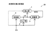
図2に示す本発明の第2原理図は、別案3に対応する原理を説明するものである。第1原理図の構成要素に加えて発振周波数制御信号(VR)を所定値にクランプするクランプ部2を備えている。クランプ部2は、発振許可信号(EN)により制御されている。
The second principle diagram of the present invention shown in FIG. 2 explains the principle corresponding to
検出部1は、電流消費の観点から、発振許可信号(EN)による制御部4の起動後に活性化されればよく、発振許可信号(EN)が出力されない発振不可状態では非活性の状態あることが好ましい。そこで、クランプ部2をそなえることにより、発振許可信号(EN)の制御を得て、発振不可状態において発振周波数制御信号(VR)を所定のクランプ値に維持しておく。このクランプ値を検出部1の入力段における非活性な信号値に設定しておけば、検出部1における検出動作を停止状態に維持しておくことができる。発振不可状態において、検出部1において不要な電流消費を将来することはなく、低消費電流化に寄与することができる。
From the viewpoint of current consumption, the
尚、検出部1を非活性化状態に維持する他の方法として、発振許可信号(EN)により検出部1自身を制御する構成とすることもできる。発振不可状態で検出部1の回路動作を非活性とすれば、発振周波数制御信号(VR)の信号値にかかわらず検出部1の動作を停止させておくことができる。
As another method for maintaining the
図3に示す本発明の第3原理図は、請求項1に対応する本発明の原理を説明するものである。第1原理図の検出部1に代えて、遅延部3を備えている。遅延部3には発振許可信号(EN)が入力され、所定遅延時間を付加した遅延信号(D)を発振部5に出力している。発振許可信号(EN)による制御部4の起動後に発振周波数制御信号(VR)が変化する過渡期間に合わせて、所定遅延時間が設定されている。
The third principle diagram of the present invention shown in FIG. 3 explains the principle of the present invention corresponding to claim 1. Instead of the
遅延部3により、発振周波数制御信号(VR)が所定信号に達するまでの過渡期間以上の所定時間を計時して遅延信号(D)を発振部5に出力する。発振部5は、発振許可信号(EN)により発振可能状態にあり、遅延信号(D)が入力された時点で発振信号を出力するように制御する。これにより、発振周波数制御信号(VR)が過渡状態を越えて安定した信号値に達した時点以後に発振部5を動作させることができ、過渡的な発振周波数制御信号(VR)の設定による不安定な発振信号が発振部5から出力されてしまうことはない。
The
本発明によれば、作動・停止の制御が可能なオシレータ回路の発振開始時における発振周波数の過渡的な不安定期間には、発振動作を停止させ又は発振信号の出力をさせないことにより、その後に出力される発振信号の発振周波数を安定した周波数とすることが可能なオシレータ回路、オシレータ回路を備えた半導体装置、及びオシレータ回路を備えた半導体記憶装置を提供することが可能となる。 According to the present invention, during the transient unstable period of the oscillation frequency at the start of oscillation of the oscillator circuit capable of operating / stopping, the oscillation operation is stopped or the oscillation signal is not output, and thereafter It is possible to provide an oscillator circuit capable of setting the oscillation frequency of the output oscillation signal to a stable frequency, a semiconductor device including the oscillator circuit, and a semiconductor memory device including the oscillator circuit.
以下、本発明のオシレータ回路、オシレータ回路を備えた半導体装置、及びオシレータ回路を備えた半導体記憶装置について具体化した第1乃至第6実施形態を図4乃至図14に基づき図面を参照しつつ詳細に説明する。
図4は、第1実施形態を示す回路図である(オシレータ回路)。図5は、第1実施形態の動作を示す動作波形図である。図6は、第2実施形態を示す回路図である(オシレータ回路)。図7は、第2実施形態の動作を示す動作波形図である。図8は、第3実施形態を示す回路図である(クランプ部)。図9は、第4実施形態を示す回路図である(クランプ部)。図10は、第5実施形態を示す回路図である(検出部)。図11は、第6実施形態を示す回路図である(オシレータ回路)。図12は、第6実施形態の動作を示す動作波形図である。図13は、オシレータ回路を備える半導体装置を示す回路ブロック図である。図14は、オシレータ回路を備える半導体記憶装置を示す回路ブロック図である。
Hereinafter, the first to sixth embodiments of the oscillator circuit, the semiconductor device provided with the oscillator circuit, and the semiconductor memory device provided with the oscillator circuit according to the present invention will be described in detail with reference to the drawings based on FIGS. Explained.
FIG. 4 is a circuit diagram showing the first embodiment (oscillator circuit). FIG. 5 is an operation waveform diagram showing the operation of the first embodiment. FIG. 6 is a circuit diagram showing the second embodiment (oscillator circuit). FIG. 7 is an operation waveform diagram showing the operation of the second embodiment. FIG. 8 is a circuit diagram showing the third embodiment (clamp portion). FIG. 9 is a circuit diagram showing the fourth embodiment (clamp portion). FIG. 10 is a circuit diagram showing the fifth embodiment (detection unit). FIG. 11 is a circuit diagram showing the sixth embodiment (oscillator circuit). FIG. 12 is an operation waveform diagram showing the operation of the sixth embodiment. FIG. 13 is a circuit block diagram illustrating a semiconductor device including an oscillator circuit. FIG. 14 is a circuit block diagram illustrating a semiconductor memory device including an oscillator circuit.
図4乃至7に示すオシレータ回路は、第1原理図(図1)に対する第1及び第2実施形態のオシレータ回路である。図4は第1実施形態のオシレータ回路である。制御部41は、従来技術の第1具体例における制御部43に備えられているスイッチ素子S100をPMOSトランジスタTP1で置き換えた構成である。また、発振部51は、従来技術の第2具体例における発振部53からスイッチ素子としてPMOSトランジスタTP4を介して発振信号OSCが出力される構成である。PMOSトランジスタTP4のゲート端子は、後述の検出部11からの出力である検出信号MONで制御される。
The oscillator circuits shown in FIGS. 4 to 7 are the oscillator circuits of the first and second embodiments corresponding to the first principle diagram (FIG. 1). FIG. 4 shows the oscillator circuit of the first embodiment. The
検出部11は、発振周波数制御信号VRがNMOSトランジスタTN1のゲート端子に入力される。NMOSトランジスタTN1のソース端子は接地電圧VSSに接続されている。ドレイン端子は、ソース端子に電源電圧VDDが接続されゲート端子に接地電圧が接続されているPMOSトランジスタTP2のドレイン端子に接続されており、この接続点を出力端子とする論理反転ゲートが構成されている。この論理反転ゲートの論理反転閾値電圧は、PMOSトランジスタTP2のコンダクタンスとNMOSトランジスタTN1のコンダクタンスとのバランスで設定され、発振部51が所定発振周波数で発振動作を行なう際の発振周波数制御信号VRの電圧値に対して論理反転するように設定されている。発振周波数制御信号VRが所定電圧値に達したことを検出することができる電圧値を閾値電圧として設定しておき、発振周波数制御信号VRが安定した電圧値を出力する状態で検出信号MONを活性化する。制御部41の起動に伴い、発振周波数制御信号VRは接地電圧VSSから所定発振周波数を指示する所定電圧値まで上昇していくので、所定電圧値に至るまでの一定の電圧値を閾値電圧として設定しておくことにより、確実に論理反転させて検出信号MONを活性化させることができる。初段の論理反転ゲートの出力は、2段のインバータ素子INV1、INV2により波形整形、駆動能力の確保、及び論理の整合等を行なった上で検出信号MONとして発振部51に出力される。
In the
発振部51では、リングオシレータの最終段のインバータ素子に代えてノア素子NOR1が備えられており、発振許可信号であるイネーブル信号ENで制御される。イネーブル信号ENがロー論理レベルとなる発振可能状態では、ノア素子NOR1は論理反転ゲートとして機能しリングオシレータが構成されるため、発振部51内での発振動作が行なわれる。一方、ノア素子NOR1の出力はPMOSトランジスタTP4を介して発振信号OSCとして出力される。PMOSトランジスタTP4は検出信号MONにより制御される。検出信号MONは、イネーブル信号ENが活性化して制御部41が起動し発振周波数制御信号VRが所定電圧値に達した段階でロー論理レベルとなり、PMOSトランジスタTP4が導通して発振信号OSCが出力される。イネーブル信号ENの活性化と共に、発振部51内のリングオシレータが構成され発振動作が開始された後、発振周波数が所定周波数に達した時点で出力信号である発振信号OSCが出力されるという2段階で発振動作が行なわれる。従って、発振信号OSCとして安定した所定発振周波数の信号が出力される。
The oscillating
図5に発振動作波形を示す。イネーブル信号ENがロー論理レベルに遷移すると、制御部41が起動すると共に発振部51においてリングオシレータが構成されて発振動作が開始される。制御部41の起動により、発振周波数制御信号VRは接地電圧VSSから所定電圧値にまで徐々に上昇するが、この過渡期間(図5中、X1)においては所定電圧値より低電圧であるため、リングオシレータへの制御電流ICは安定状態に比して多大となる。そのため、リングオシレータは高周波数で発振する(ノードN1)。しかし検出信号MONは非活性でありPMOSトランジスタTP4は非導通状態にあるので、発振信号OSCに高周波数の発振信号が出力されることはない。その後、検出部11により発振周波数制御信号VRが所定電圧値に達したことが検出されて検出信号MONが反転する。その時点でPMOSトランジスタTP4が導通して、所定発振周波数に安定して発振しているリングオシレータの発振信号が発振信号OSCとして出力される。
FIG. 5 shows an oscillation operation waveform. When the enable signal EN transitions to the low logic level, the
図6は第2実施形態のオシレータ回路である。第1実施形態の制御部41に代えて、従来技術の第3具体例における制御部44に備えられているスイッチ素子S102をNMOSトランジスタTN2で置き換えた構成の制御部42を備えている。また、第1実施形態の発振部51におけるPMOSトランジスタTP4を外し、イネーブル信号ENと検出信号MONとが入力されるノア素子NOR2とインバータ素子INV3を介して、発振開始信号ONがノア素子NOR1に入力されている。発振信号OSCはノア素子NOR1から出力される構成である。
FIG. 6 shows an oscillator circuit according to the second embodiment. Instead of the
検出部12は、第1実施形態の検出部11におけるインバータ素子INV2を外した構成であり、ローアクティブの検出信号MONを出力する構成である。検出部12の初段には、検出部11の初段と同様な論理反転ゲートが備えられている。制御部42の起動に伴い、発振周波数制御信号VRは高い電圧レベルから所定発振周波数を指示する所定電圧値まで下降していくので、所定電圧値に至るまでの所定の電圧値を閾値電圧として設定しておくことにより確実に論理反転させて検出信号MONを活性化させることができる。制御部42の構成が第1実施形態の制御部41とは反転した極性を有して動作するので、これに合わせて検出部12のインバータ素子の構成が第1実施形態の検出部11に比して1段少ない構成となっている。
The
図7に発振動作波形を示す。イネーブル信号ENがロー論理レベルに遷移すると、制御部42が起動して発振周波数制御信号VRは電源電圧VDDからPMOSトランジスタの閾値電圧Vthpだけ降下した高電圧レベル(VDD−Vthp)から所定電圧値にまで徐々に下降するが、この過渡期間(図7中、X2)においては所定電圧値より高電圧であるため、リングオシレータへの制御電流ICは安定状態に比して少ない。その時の検出部初段は反転していないので、検出信号MONはハイ論理レベルを維持しており、ノア素子NOR2を介して発振信号OSCをローレベルに固定している。即ち、リングオシレータにおける発振動作を停止すると共に発振信号OSCもローレベルに固定している。その後、検出部12により発振周波数制御信号VRが所定電圧値に達したことが検出されて検出信号MONがロー論理レベルに反転する。その時点でノア素子NOR2の入力信号は共にロー論理レベルとなり出力がハイ論理レベルに反転して、ノア素子NOR1を論理反転ゲートとして機能させリングオシレータでの発振動作を開始させる。この発振動作は同時に発振信号OSCからも出力される。この時点では、発振周波数制御信号VRが所定電圧値に達しているので、発振動作は所定発振周波数に安定して行なわれることとなり、安定した発振出力が発振信号OSCとして出力される。
FIG. 7 shows an oscillation operation waveform. When the enable signal EN transitions to the low logic level, the
以上に説明したように、第1及び第2実施形態によれば、検出部11、12の検出結果である検出信号MONに応じて、発振周波数制御信号VRで設定される所望の発振周波数で発振動作を行なわせることができる。発振許可信号であるイネーブル信号ENにより動作を開始する制御部41、42からの発振周波数制御信号VRが安定しない過渡期間(図5中、X1、図7中、X2)においても、不安定な発振動作をすることがなく安定した発振周波数で発振させることができる。
As described above, according to the first and second embodiments, oscillation is performed at a desired oscillation frequency set by the oscillation frequency control signal VR according to the detection signal MON that is the detection result of the
また、検出部11、12の初段回路において、発振周波数制御信号VRの信号値を所定周波数に対応する信号値と比較して、発振部51、52における発振周波数を所定周波数とすることができる。
In the first stage circuits of the
アナログ電圧値である発振周波数制御信号VRを、所定発振周波数に対応する信号値を閾値電圧とする、検出部11、12の初段回路の論理反転ゲートで検出することができる。検出信号MONをディジタル信号として取り出すことができ、後段の発振部51、52での発振開始等の処理をディジタル信号により行なうことができる。これにより小規模な回路で低消費電流動作により高速な処理を行なうことができる。
The oscillation frequency control signal VR, which is an analog voltage value, can be detected by the logic inversion gates of the first stage circuits of the
また、発振部51のノア素子NOR1、発振部52のノア素子NOR2が、信号合成部として機能することにより、発振許可信号であるイネーブル信号ENと検出信号MONとが論理合成されて出力されるので、両信号が共にロー論理レベルにあることを検出した上で、作動制御手段であるリングオシレータの最終段を構成するノア素子NOR1を制御することができる。
Since the NOR element NOR1 of the
図8乃至10に示す第3乃至第5実施形態は、第2原理図(図2)に対する実施形態である。図8の第3実施形態ではクランプ部21を示している。検出部11又は12に入力される発振周波数制御信号VRと、所定電圧Vとの間にNMOSトランジスタTN3が備えられており、イネーブル信号ENで制御されている。ここでは、イネーブル信号ENはローアクティブな信号である場合を例示している。即ち、イネーブル信号ENがロー論理レベルとなり発振可能状態にあるときは、NMOSトランジスタTN3は非導通となり、制御部で生成される発振周波数制御信号VRが検出部11又は12に入力され検出動作が行なわれる。イネーブル信号ENがハイ論理レベルとなり発振不可状態にあるときは、NMOSトランジスタTN3が導通して、発振周波数制御信号VRを所定電圧Vにクランプされる。ここで所定電圧Vは、検出部11又は12の初段回路における論理反転前の電圧に設定されているので、検出信号MONが出力されることはない。具体的には、発振不可状態で発振周波数制御信号VRが接地電圧VSSになる第1実施形態に対しては、所定電圧Vを接地電圧VSSに設定し、発振不可状態で発振周波数制御信号VRが(VDD−Vthp)の高い電圧になる第2実施形態に対しては、所定電圧(VDD−Vthp)又はそれ以上の電圧に設定すればよい。
The third to fifth embodiments shown in FIGS. 8 to 10 are embodiments corresponding to the second principle diagram (FIG. 2). In the third embodiment of FIG. 8, the
図9の第4実施形態ではクランプ部22を示している。第3実施形態のクランプ部21に加えて、発振不可状態において、検出部11又は12の入力端子と発振周波数制御信号VRを出力する制御部の出力端子とを遮断するトランスファゲートT1を備えている。トランスファゲートT1のPMOSトランジスタのゲート端子にはローアクティブのイネーブル信号ENが入力され、NMOSトランジスタのゲート端子にはイネーブル信号ENがインバータ素子INV4で反転されて入力される。イネーブル信号ENがロー論理レベルとなり発振可能状態にあるときは、NMOSトランジスタTN3が非導通となると共に、トランスファゲートT1が導通して発振周波数制御信号VRが検出部11又は12に入力され検出動作が行なわれる。イネーブル信号ENがハイ論理レベルとなり発振不可状態にあるときは、NMOSトランジスタTN3が導通すると共に、トランスファゲートT1が非導通となって検出部11又は12の入力端子が所定電圧Vにクランプされる。
In the fourth embodiment of FIG. 9, the
図10の第5実施形態は、検出部13を示している。検出部13は、イネーブル信号ENに応じて活性・非活性が切り替えられる回路構成である。第1実施形態の検出部11の初段回路にNMOSトランジスタTN4を付加した構成である。NMOSトランジスタTN4は、NMOSトランジスタTN1と初段回路の出力端子との間に接続され、ゲート端子にはイネーブル信号ENがインバータ素子INV5で反転されて入力されている。イネーブル信号ENがロー論理レベルとなり発振可能状態にあるときは、NMOSトランジスタTN4が導通して初段回路が活性化されるため検出動作が行なわれる。イネーブル信号ENがハイ論理レベルとなり発振不可状態にあるときは、NMOSトランジスタTN4が非導通となり、初段回路の出力端子は電源電圧VDDに固定され検出動作は行なわれない。
The fifth embodiment of FIG. 10 shows the
尚、第5実施形態の検出部13では、検出部11に対応する回路構成を例示したが、第2実施形態の検出部12に対応する回路構成とすることもできる。この場合には、検出部13におけるNMOSトランジスタTN4に代えて、PMOSトランジスタTP2と初段回路の出力端子との間にPMOSトランジスタを挿入し、ゲート端子にはイネーブル信号ENを入力すればよい。イネーブル信号ENがロー論理レベルとなり発振可能状態にあるときは、新たに接続されたPMOSトランジスタが導通して検出動作が行なわれる。イネーブル信号ENがハイ論理レベルとなり発振不可状態にあるときは、新たに接続されたPMOSトランジスタが非導通となり、初段回路の出力端子は接地電圧VSSに固定され検出動作は行なわれない。
In addition, in the
以上に説明したように、第3、第4実施形態によれば、発振周波数制御信号VRを所定発振周波数に対応する信号値以外の信号値に維持しておくことができ、検出部11又は12での検出動作を停止させることができ、発振出力を止めておくことができる。 As described above, according to the third and fourth embodiments, the oscillation frequency control signal VR can be maintained at a signal value other than the signal value corresponding to the predetermined oscillation frequency. The detection operation can be stopped and the oscillation output can be stopped.
また、このときの所定クランプ値は、第1実施形態の構成の場合には接地電圧VSSとし、第2実施形態の構成の場合には電源電圧VDD等の(VDD−Vthp)より高い電圧レベルとしておけば、確実に検出部11又は12での検出動作を停止させることができ、発振出力を止めておくことができる。
Further, the predetermined clamp value at this time is the ground voltage VSS in the case of the configuration of the first embodiment, and is set to a voltage level higher than (VDD−Vthp) such as the power supply voltage VDD in the case of the configuration of the second embodiment. If so, the detection operation in the
また、第5実施形態によれば、イネーブル信号ENにより、検出部13自体の回路動作を非活性とすることができるので、発振不可状態において不要な電流消費を低減することができる。
Further, according to the fifth embodiment, since the circuit operation of the
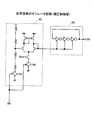
図11に示すオシレータ回路は、第3原理図(図3)に対する第6実施形態のオシレータ回路である。第2実施形態のオシレータ回路における検出部12に代えて遅延部31を備えている。また、発振部53では、発振部52における2入力のノア素子NOR2に代えて3入力のノア素子NOR3を備えている。ノア素子NOR3の各入力端子には、イネーブル信号ENが直接入力されている他、遅延部31の第1遅延部D1からの遅延信号、及び遅延部31の第2遅延部D2からの遅延信号が各々入力されている。
The oscillator circuit shown in FIG. 11 is the oscillator circuit of the sixth embodiment corresponding to the third principle diagram (FIG. 3). A
第1遅延部D1は、偶数段のインバータ素子(図11は、4段の場合を例示。)が直列に接続されて構成されている。第2遅延部D2は、イネーブル信号ENがロー論理レベルに遷移した後、所定遅延時間を計時する遅延回路を構成している。イネーブル信号ENはインバータ素子で反転されてナンド素子NA1の各々の入力端子に入力される。一方の入力端子には直接入力され、他方の入力端子には、インバータ素子やCR遅延素子等で構成される遅延ユニットτを介して所定遅延時間の遅延を受けた信号が入力される。これにより、ナンド素子NA1の出力端子にはイネーブル信号ENの反転信号の立ち上がりエッジに対して遅延した信号が出力される。この遅延信号がインバータ素子で反転されることにより、イネーブル信号ENの反転信号の立ち上がりエッジから遅延ユニットτで設定されている所定遅延時間のパルス幅を有するハイ論理レベルのパルス信号が遅延信号Dとして得られる。ここで、イネーブル信号ENの反転信号の立ち上がりエッジとは、イネーブル信号ENのロー論理レベルへの立ち下がりエッジであり発振開始のタイミングに対応する。 The first delay unit D1 is configured by connecting even-numbered inverter elements (FIG. 11 illustrates the case of four stages) in series. The second delay unit D2 constitutes a delay circuit that measures a predetermined delay time after the enable signal EN transitions to a low logic level. The enable signal EN is inverted by the inverter element and input to each input terminal of the NAND element NA1. A signal that has been delayed by a predetermined delay time is input to one input terminal via a delay unit τ composed of an inverter element, a CR delay element, and the like. As a result, a signal delayed with respect to the rising edge of the inverted signal of the enable signal EN is output to the output terminal of the NAND element NA1. When this delay signal is inverted by the inverter element, a high logic level pulse signal having a pulse width of a predetermined delay time set by the delay unit τ from the rising edge of the inverted signal of the enable signal EN is used as the delay signal D. can get. Here, the rising edge of the inverted signal of the enable signal EN is the falling edge of the enable signal EN to the low logic level and corresponds to the timing of starting oscillation.
尚、イネーブル信号ENがロー論理レベルに遷移してから遅延信号Dがハイ論理レベルにセットされるまでの間には回路上の遅延時間が存在するので、発振部53のインバータ素子INV3から出力される発振開始信号ONにロー論理レベルのハザードが発生する可能性がある。第1遅延部D1はこの対策として備えられている。即ち、第1遅延部D1による遅延信号により、イネーブル信号ENのロー論理レベルへの遷移からの回路上の遅延時間の間に、ノア素子NOR3の少なくとも1つの入力端子にハイ論理レベルが入力されていることとなり、ハザードを防止することができる。
Since there is a delay time on the circuit after the enable signal EN transitions to the low logic level and before the delay signal D is set to the high logic level, it is output from the inverter element INV3 of the
図12に発振動作開始時の動作波形を示す。イネーブル信号ENがロー論理レベルに遷移すると、制御部42が起動して発振周波数制御信号VRは高電圧レベル(VDD−Vthp)から所定電圧値にまで徐々に下降する。しかしながらこの過渡期間(図12中、X2)は、発振周波数制御信号VRが所定電圧値より高電圧であるため、リングオシレータへの制御電流ICは安定状態に比して少ない。そこでこの期間の発振動作を止めておくために、遅延部31において、第1遅延部D1の遅延時間に引き続いて第2遅延部D2によりハイ論理レベルの遅延信号Dを出力する。これにより、発振部53のノア素子NOR3のうち少なくとも1つの入力端子はハイ論理レベルに維持されることとなり、発振開始信号ONはハイ論理レベルに維持される。そのため、発振部53のリングオシレータが動作することはない。この期間は、第2遅延部D2の遅延ユニットτで設定される所定遅延時間の間、遅延信号Dがハイ論理レベルに維持されることにより継続する。所定遅延時間の後、遅延信号Dがロー論理レベルに反転すると、ノア素子NOR3の他の入力端子に入力されている信号もロー論理レベルであるので、発振開始信号ONがロー論理レベルに反転して発振部53における発振動作が開始され、発振信号OSCが出力される。所定遅延時間を発振周波数制御信号VRが所定電圧値に達する時点以降に設定しておけば、発振動作は安定した所定発振周波数で行なわれることとなり、安定した発振出力として発振信号OSCが出力される。
FIG. 12 shows an operation waveform at the start of the oscillation operation. When the enable signal EN transitions to the low logic level, the
以上に説明したように、第6実施形態によれば、発振許可信号であるイネーブル信号ENにより動作を開始する制御部42からの発振周波数制御信号VRの信号値が、安定する時間を所定遅延時間として遅延部31の第2遅延部D2に設定することができ、発振周波数制御信号VRが安定して所定発振周波数に対応する信号値に達した時点以後に安定した発振信号OSCを得ることができる。
As described above, according to the sixth embodiment, the time during which the signal value of the oscillation frequency control signal VR from the
また、ここで、第2遅延部D2における遅延ユニットを構成するCR遅延回路等を、制御部42における制御電流ICの電流系路等の抵抗成分と、PMOSトランジスタTP1、TP3のゲート容量等の容量成分とで構成されるCR遅延回路構成の時定数と対応させておけば、発振周波数制御信号VRが安定状態に達するまでの時間と同等の時間を遅延部31により計時することができる。遅延部31として最適なタイミングで所定遅延時間を計時することができる。
Also, here, the CR delay circuit constituting the delay unit in the second delay unit D2, the resistance component such as the current path of the control current IC in the
また、以上に説明した第1、第2、及び第6実施形態によれば、発振部51乃至53からの発振信号OSCの出力は、作動制御手段であるノア素子NOR1によるリングオシレータの発振動作の作動・停止、又は出力制御手段であるPMOSトランジスタTP4による発振信号OSCの出力・停止のいずれの手段によっても制御することができ、これらの2つの手段を共に使用して制御することもできる。
Further, according to the first, second, and sixth embodiments described above, the output of the oscillation signal OSC from the
また、第1実施形態の発振部51のように、イネーブル信号ENがノア素子NOR1を活性化して発振動作を開始し、検出信号MONがPMOSトランジスタTP4を活性化して発振信号OSCを出力する2段階の構成とすれば、検出信号MONによる発振信号OSCの出力に対して、イネーブル信号ENによるリングオシレータの発振動作の開始を先行させておくことができ、発振信号OSCを出力する際に、発振部51における発振動作を安定化させルことができる。また、この2段階構成は、第2実施形態の発振部52、第6実施形態の発振部53にも同様に適用することができる。
Further, as in the
以上に説明したオシレータ回路を、オシレータ回路100に代えて半導体装置1000(図13)や半導体記憶装置2000(図14)に備えることにより、半導体装置1000や半導体記憶装置2000は、電圧発生回路である昇圧/負電源回路200においてオシレータ回路から出力される発振信号OSCに応じた電圧を安定して発生することができる。また、リフレッシュ制御回路300においてオシレータ回路から出力される発振信号OSCに応じて安定したリフレッシュ周期で制御することができる。
By providing the oscillator circuit described above in the semiconductor device 1000 (FIG. 13) or the semiconductor memory device 2000 (FIG. 14) instead of the
これにより、イネーブル信号ENにより動作を開始する制御部41、42からの発振周波数制御信号VRが安定しない過渡期間に、不安定な発振信号OSCが昇圧/負電現回路200やリフレッシュ制御回路300に出力されることはなく、安定した回路動作をさせることができる。
As a result, an unstable oscillation signal OSC is output to the boost / negative
具体的には、不安定な高周波数の発振信号OSCが出力されることによる、多大な消費電流やこれに伴う電源電圧の電圧降下による誤動作、あるいは過度な電圧発生による半導体装置1000や半導体記憶装置2000における信頼性上の問題等が生ずることはない。また、逆に不安定な低周波数の発振信号OSCが出力されることによる、トランジスタ特性の変動やこれに伴うノイズ耐性の悪化、あるいは半導体記憶装置2000における記憶データの消失等が生ずることはない。ここで、トランジスタ特性変動やノイズ耐性の悪化とは、MOSトランジスタにおけるバックゲートバイアス電圧の変動等が考えられる。
Specifically, the
尚、本発明は前記第1乃至第6実施形態に限定されるものではなく、本発明の趣旨を逸脱しない範囲内で種々の改良、変形が可能であることは言うまでもない。
例えば、本実施形態では、電流駆動型のオシレータ回路について例示したが、本発明はこれに限定されるものではなく、図21に例示した電圧駆動型のオシレータ回路においても同様に適用することができる。
また、電流駆動型、電圧駆動型の何れの方式においても、制御すべき駆動電流や駆動電圧は、高電源電圧側に備える構成とすることも、低電源電圧側に備える構成とすることもできる。更に、高電源電圧側及び低電源電圧側の双方に備える構成とすることもできる。この場合、駆動電流や駆動電圧の挿入位置により制御部の回路構成を適宜変更することは言うまでもない。
また、発振部における発振動作の作動・停止については、第1実施形態において、リングオシレータの動作制御をイネーブル信号ENにより行い、発振信号OSCの出力制御を検出信号MONにより行なう構成を示し、第2及び第6実施形態については、リングオシレータの動作制御を、イネーブル信号ENと、検出信号MONあるいは遅延信号Dとの論理合成により生成された発振開始信号ONにより行なう場合について例示した。しかしながら、本発明はこれに限定されるものではなく、制御信号と発振動作の作動・停止手段との組み合わせについては例示された組み合わせ以外にも任意に設定することができる。
また、発振周波数制御信号VRにより設定される発振周波数は固定として説明したが、制御部における抵抗素子を可変とする構成とすれば、抵抗値に応じて発振周波数制御信号VRの電圧レベルを可変とすることができ、発振周波数を可変することができる。このとき、可変抵抗としては、抵抗素子を切り替えることのほか、ゲート端子へのバイアスを可変とすることによりMOSトランジスタのオン抵抗を利用することもできる。
また、発振部については、リングオシレータで構成する場合について説明したが、本発明はこれに限定されるものではなく、双安定マルチバイブレータや容量成分への充放電を繰り返す方式等、発振動作を行なう回路構成であれば回路方式にかかわらず適用することができる。
The present invention is not limited to the first to sixth embodiments, and it goes without saying that various improvements and modifications can be made without departing from the spirit of the present invention.
For example, in the present embodiment, the current-driven oscillator circuit is illustrated, but the present invention is not limited to this, and can be similarly applied to the voltage-driven oscillator circuit illustrated in FIG. .
In either the current drive type or the voltage drive type, the drive current and drive voltage to be controlled can be provided on the high power supply voltage side or on the low power supply voltage side. . Furthermore, it can also be set as the structure provided in both the high power supply voltage side and the low power supply voltage side. In this case, it goes without saying that the circuit configuration of the control unit is appropriately changed depending on the insertion position of the drive current or drive voltage.
As for the operation / stop of the oscillating operation in the oscillating unit, the first embodiment shows a configuration in which the operation control of the ring oscillator is performed by the enable signal EN, and the output control of the oscillation signal OSC is performed by the detection signal MON. In the sixth embodiment, the operation of the ring oscillator is controlled by the oscillation start signal ON generated by logic synthesis of the enable signal EN and the detection signal MON or the delay signal D. However, the present invention is not limited to this, and the combination of the control signal and the oscillation operation start / stop means can be arbitrarily set in addition to the illustrated combinations.
Further, although the description has been made assuming that the oscillation frequency set by the oscillation frequency control signal VR is fixed, if the resistance element in the control unit is made variable, the voltage level of the oscillation frequency control signal VR can be made variable according to the resistance value. The oscillation frequency can be varied. At this time, as the variable resistor, in addition to switching the resistance element, the on-resistance of the MOS transistor can be used by changing the bias to the gate terminal.
In addition, the case where the oscillation unit is configured by a ring oscillator has been described, but the present invention is not limited to this, and an oscillation operation such as a bistable multivibrator or a method of repeatedly charging and discharging a capacitive component is performed. Any circuit configuration can be applied regardless of the circuit system.
(付記1) 発振許可信号に応じて発振動作が可能となる発振部と、
前記発振許可信号に応じて発振周波数を制御する発振周波数制御信号を前記発振部に向けて出力する制御部と、
前記発振周波数制御信号を検出し、検出結果に応じて前記発振部を制御する検出信号を出力する検出部とを備えることを特徴とするオシレータ回路。
(付記2) 前記検出部は、
入力される前記発振周波数制御信号の信号値と、所定発振周波数に対応する信号値とを比較する比較部を備えることを特徴とする付記1に記載のオシレータ回路。
(付記3) 前記信号値は、アナログ電圧値であり、
前記比較部は、前記所定発振周波数に対応する信号値を閾値電圧とする論理ゲート素子を含むことを特徴とする付記2に記載のオシレータ回路。
(付記4) 前記検出部は、前記発振許可信号により制御され、発振不可状態において非活性化されることを特徴とする付記1に記載のオシレータ回路。
(付記5) 前記発振許可信号により制御され、発振不可状態において前記発振周波数制御信号を所定クランプ値にクランプするクランプ部を備えることを特徴とする付記1に記載のオシレータ回路。
(付記6) 前記所定クランプ値は、前記発振部を、発振停止状態又は発振信号の出力停止状態に制御する信号値であることを特徴とする付記5に記載のオシレータ回路。
(付記7) 発振許可信号に応じて発振動作が可能となる発振部と、
前記発振許可信号に応じて発振周波数を制御する発振周波数制御信号を前記発振部に向けて出力する制御部と、
前記発振許可信号に対して所定遅延時間を付加した遅延信号を、前記発振部に出力する遅延部とを備えることを特徴とするオシレータ回路。
(付記8) 前記所定遅延時間は、前記発振許可信号に応じて、前記発振周波数制御信号の信号値が所定発振周波数に対応する信号値に達するまでの時間以上の時間であることを特徴とする付記7に記載のオシレータ回路。
(付記9) 前記遅延部は、
前記発振周波数制御信号を生成する回路構成と同等の回路構成を有することを特徴とする付記7に記載のオシレータ回路。
(付記10) 前記発振部は、
前記発振動作の作動制御手段又は発振信号の出力制御手段のうち少なくとも何れか一方を備え、
前記検出信号又は前記遅延信号による制御は、前記発振許可信号による発振可能状態において前記発振周波数制御信号が所定発振周波数を指示する場合に、前記作動制御手段の活性化による発振動作の開始、又は前記出力制御手段の活性化による前記発振信号の出力のうち少なくとも何れか一方を行なうことを特徴とする付記1又は7に記載のオシレータ回路。
(付記11) 前記発振部は、
前記発振許可信号と、前記検出信号又は前記遅延信号との信号の合成を行なう信号合成部を備え、
前記信号合成部からの出力信号に応じて、前記作動制御手段又は前記出力制御手段のうち少なくとも何れか一方の活性化を行なうことを特徴とする付記10に記載のオシレータ回路。
(付記12) 前記発振部は、
前記発振許可信号により前記作動制御手段が活性化され、
前記検出信号又は前記遅延信号により前記出力制御手段が活性化されることを特徴とする付記10に記載のオシレータ回路。
(付記13) 前記発振部は、駆動電源電流により発振周波数が制御され、
前記発振周波数制御信号は、前記駆動電源電流であるか、又は、
前記駆動電源電流を供給するための定電流源を制御する電流信号又は電圧信号であることを特徴とする付記1又は7に記載のオシレータ回路。
(付記14) 前記発振部は、駆動電源電圧により発振周波数が制御され、
前記発振周波数制御信号は、前記駆動電源電圧であるか、又は、
前記駆動電源電圧を供給するための定電圧源を制御する電流信号又は電圧信号であることを特徴とする付記1又は7に記載のオシレータ回路。
(付記15) 付記1又は7に記載のオシレータ回路と、
前記オシレータ回路から出力される発振信号に応じた電圧を発生する電圧発生回路とを備えることを特徴とする半導体装置。
(付記16) 前記電圧発生回路は、昇圧回路であり、前記発振信号に応じた昇圧電圧を発生することを特徴とする付記15に記載の半導体装置。
(付記17) 前記電圧発生回路は、負電圧発生回路であり、前記発振信号に応じた負電圧を発生することを特徴とする付記15に記載の半導体装置。
(付記18) 付記1又は7に記載のオシレータ回路と、
前記オシレータ回路から出力される発振信号に応じた電圧を発生する電圧発生回路とを備えることを特徴とする半導体記憶装置。
(付記19) 前記電圧発生回路は、昇圧回路であり、前記発振信号に応じた昇圧電圧を発生することを特徴とする付記18に記載の半導体記憶装置。
(付記20) 前記電圧発生回路は、負電圧発生回路であり、前記発振信号に応じた負電圧を発生することを特徴とする付記18に記載の半導体記憶装置。
(付記21) 付記1又は7に記載のオシレータ回路と、
前記オシレータ回路から出力される発振信号に応じてリフレッシュ周期を制御するリフレッシュ制御回路とを備えることを特徴とする半導体記憶装置。
(付記22) 発振許可信号に応じて発振動作が可能となる発振部と、前記発振許可信号に応じて発振周波数を制御する発振周波数制御信号を前記発振部に向けて出力する制御部とを有するオシレータ回路の制御方法であって、
前記発振許可信号による発振可能状態において、前記発振周波数制御信号が所定発振周波数を指示する状態に達した時点以後の所定タイミングで、前記発振部の発振動作の開始、又は前記発振部からの発振信号の出力のうち少なくとも何れか一方を行なうことを特徴とするオシレータ回路の制御方法。
(付記23) 前記所定タイミングは、前記発振周波数制御信号の信号値と所定発振周波数に対応する信号値との比較により検出されることを特徴とする付記22に記載のオシレータ回路の制御方法。
(付記24) 前記発振許可信号による発振不可状態において、前記発振周波数制御信号の信号値と前記所定発振周波数に対応する信号値との比較動作は、非活性化されることを特徴とする付記23に記載のオシレータ回路の制御方法。
(付記25) 前記発振許可信号による発振不可状態において、前記発振周波数制御信号は、前記所定発振周波数を指示する状態に達せず非活性な信号値に維持されることを特徴とする付記23に記載のオシレータ回路の制御方法。
(付記26) 前記所定タイミングは、前記発振許可信号からの所定遅延時間の経過以後のタイミングとして設定されることを特徴とする付記22に記載のオシレータ回路の制御方法。
(付記27) 前記所定遅延時間は、前記発振許可信号に応じて、前記発振周波数制御信号の信号値が所定発振周波数に対応する信号値に達するまでの時間以上の時間であることを特徴とする付記26に記載のオシレータ回路の制御方法。
(付記28) 前記発振許可信号による発振可能状態において前記発振部の発振動作を開始し、
前記所定タイミングで前記発振部からの発振信号の出力を行なうことを特徴とする付記22に記載のオシレータ回路の制御方法。
(Appendix 1) An oscillating unit capable of oscillating according to an oscillation enabling signal;
A control unit that outputs an oscillation frequency control signal for controlling an oscillation frequency according to the oscillation enable signal to the oscillation unit;
An oscillator circuit comprising: a detection unit that detects the oscillation frequency control signal and outputs a detection signal for controlling the oscillation unit according to a detection result.
(Supplementary Note 2) The detection unit includes:
The oscillator circuit according to
(Supplementary Note 3) The signal value is an analog voltage value,
The oscillator circuit according to
(Supplementary note 4) The oscillator circuit according to
(Supplementary Note 5) The oscillator circuit according to
(Additional remark 6) The said predetermined clamp value is a signal value which controls the said oscillation part to an oscillation stop state or the output stop state of an oscillation signal, The oscillator circuit of
(Appendix 7) An oscillation unit that can oscillate according to an oscillation enable signal;
A control unit that outputs an oscillation frequency control signal for controlling an oscillation frequency according to the oscillation enable signal to the oscillation unit;
An oscillator circuit comprising: a delay unit that outputs a delay signal obtained by adding a predetermined delay time to the oscillation enable signal to the oscillation unit.
(Additional remark 8) The said predetermined delay time is time more than time until the signal value of the said oscillation frequency control signal reaches the signal value corresponding to a predetermined oscillation frequency according to the said oscillation permission signal, It is characterized by the above-mentioned. The oscillator circuit according to appendix 7.
(Supplementary Note 9) The delay unit is
The oscillator circuit according to appendix 7, wherein the oscillator circuit has a circuit configuration equivalent to a circuit configuration for generating the oscillation frequency control signal.
(Supplementary Note 10) The oscillation unit is
Comprising at least one of the oscillation operation control means or the oscillation signal output control means,
The control by the detection signal or the delay signal is the start of the oscillation operation by the activation of the operation control means when the oscillation frequency control signal indicates a predetermined oscillation frequency in the oscillation enabled state by the oscillation permission signal, or 8. The oscillator circuit according to
(Additional remark 11)
A signal synthesis unit for synthesizing the oscillation enable signal and the detection signal or the delayed signal;
The oscillator circuit according to
(Supplementary note 12)
The operation control means is activated by the oscillation permission signal,
The oscillator circuit according to
(Supplementary Note 13) The oscillation frequency of the oscillation unit is controlled by a drive power supply current.
The oscillation frequency control signal is the drive power supply current, or
The oscillator circuit according to
(Supplementary Note 14) The oscillation frequency of the oscillation unit is controlled by a drive power supply voltage.
The oscillation frequency control signal is the drive power supply voltage, or
The oscillator circuit according to
(Supplementary Note 15) The oscillator circuit according to
A semiconductor device comprising: a voltage generation circuit that generates a voltage corresponding to an oscillation signal output from the oscillator circuit.
(Supplementary note 16) The semiconductor device according to supplementary note 15, wherein the voltage generation circuit is a booster circuit and generates a boosted voltage corresponding to the oscillation signal.
(Supplementary note 17) The semiconductor device according to supplementary note 15, wherein the voltage generation circuit is a negative voltage generation circuit and generates a negative voltage corresponding to the oscillation signal.
(Supplementary Note 18) The oscillator circuit according to
A semiconductor memory device comprising: a voltage generation circuit that generates a voltage corresponding to an oscillation signal output from the oscillator circuit.
(Supplementary note 19) The semiconductor memory device according to supplementary note 18, wherein the voltage generation circuit is a booster circuit and generates a boosted voltage corresponding to the oscillation signal.
(Supplementary note 20) The semiconductor memory device according to supplementary note 18, wherein the voltage generation circuit is a negative voltage generation circuit and generates a negative voltage corresponding to the oscillation signal.
(Supplementary Note 21) The oscillator circuit according to
A semiconductor memory device comprising: a refresh control circuit that controls a refresh cycle in accordance with an oscillation signal output from the oscillator circuit.
(Additional remark 22) It has an oscillation part which can oscillate according to an oscillation permission signal, and a control part which outputs an oscillation frequency control signal which controls an oscillation frequency according to the oscillation permission signal toward the oscillation part A method of controlling an oscillator circuit,
In the oscillation enabled state by the oscillation enable signal, at the predetermined timing after the oscillation frequency control signal reaches the state indicating the predetermined oscillation frequency, the oscillation operation of the oscillation unit starts or the oscillation signal from the oscillation unit A method for controlling an oscillator circuit, wherein at least one of the outputs is performed.
(Supplementary note 23) The method of controlling an oscillator circuit according to
(Supplementary note 24) The supplementary note 23 is characterized in that the comparison operation between the signal value of the oscillation frequency control signal and the signal value corresponding to the predetermined oscillation frequency is deactivated in the oscillation disabled state by the oscillation permission signal. A method for controlling the oscillator circuit according to
(Supplementary note 25) The supplementary note 23, wherein the oscillation frequency control signal is maintained at an inactive signal value without reaching the state for instructing the predetermined oscillation frequency in the oscillation disabled state by the oscillation permission signal. Control method of the oscillator circuit of the present invention.
(Additional remark 26) The said predetermined timing is set as a timing after progress of the predetermined delay time from the said oscillation permission signal, The control method of the oscillator circuit of
(Additional remark 27) The said predetermined delay time is time more than time until the signal value of the said oscillation frequency control signal reaches the signal value corresponding to a predetermined oscillation frequency according to the said oscillation permission signal, It is characterized by the above-mentioned. 27. A method of controlling the oscillator circuit according to appendix 26.
(Supplementary Note 28) In the oscillation enabled state by the oscillation enable signal, the oscillation operation of the oscillation unit is started,
23. The method of controlling an oscillator circuit according to
ここで、付記3によれば、アナログ電圧値である発振周波数制御信号を、所定発振周波数に対応する信号値を閾値電圧として調整した論理ゲート素子で検出することができ、検出結果としてディジタル信号を得ることができる。後段の処理をディジタル信号により行なうことができ、小規模な回路で低消費電流動作により高速な処理を行なうことができる。
また、付記4によれば、発振許可信号により検出部の活性・非活性を制御することができるので、発振不可状態において検出部を非活性として、不要な電流消費を低減することができる。
また、付記9によれば、制御部において発振許可信号に応じて発振周波数制御信号を生成する回路構成と同等の回路構成で所定遅延時間を計時する回路を構成しておけば、最適なタイミングで所定遅延時間を構成することができる。
また、付記11によれば、発振許可信号と、検出信号又は遅延信号とが信号合成部により合成されて出力信号として出力されるので、両信号が所定の状態にあることを検出した上で、作動制御手段又は出力制御手段を制御することができる。
Here, according to
Further, according to
Further, according to Supplementary Note 9, if a circuit for measuring a predetermined delay time is configured with a circuit configuration equivalent to a circuit configuration for generating an oscillation frequency control signal in response to an oscillation enable signal in the control unit, an optimal timing can be obtained. A predetermined delay time can be configured.
Further, according to
1、11、12、13 検出部
2、21、22 クランプ部
3、31 遅延部
4、41、42、43、44、45 制御部
5、51、52、53、54、55 発振部
10 オシレータ回路(第1原理)
20 オシレータ回路(第2原理)
30 オシレータ回路(第3原理)
100 オシレータ回路(従来技術)
200 昇圧/負電源回路
300 リフレッシュ制御回路
400、410 内部回路
500 メモリセル
1000 半導体装置
2000 半導体記憶装置
D1 第1遅延部
D2 第2遅延部
D 遅延信号
EN イネーブル信号
MON 検出信号
OSC 発振信号
ON 発振開始信号
VR 発振周波数制御信号
DESCRIPTION OF
20 Oscillator circuit (second principle)
30 Oscillator circuit (third principle)
100 Oscillator circuit (prior art)
200 Booster / Negative
Claims (11)
前記発振許可信号に応じて起動し、発振周波数を制御する発振周波数制御信号を前記発振部に向けて出力する制御部と、
前記発振許可信号に対して前記発振周波数制御信号が安定する遅延時間を付加した遅延信号を前記発振部に出力して、前記遅延信号に応じて前記発振部の前記発振動作を開始させる遅延部とを備えることを特徴とするオシレータ回路。 An oscillation unit whose oscillation operation is controlled according to the oscillation enable signal;
A control unit that starts in response to the oscillation permission signal and outputs an oscillation frequency control signal that controls an oscillation frequency toward the oscillation unit;
Wherein the oscillation frequency control signal to the oscillation enable signal is output before Symbol oscillation unit delay signal obtained by adding the delay time to stabilize, delay unit to start the oscillation operation of the oscillation portion in response to said delay signal An oscillator circuit comprising:
前記発振動作の作動制御手段又は発振信号の出力制御手段のうち少なくとも何れか一方を備え、
前記遅延信号による制御は、前記発振許可信号による発振可能状態において前記発振周波数制御信号が所定発振周波数を指示する場合に、前記作動制御手段の活性化による発振動作の開始、又は前記出力制御手段の活性化による前記発振信号の出力のうち少なくとも何れか一方を行なうことを特徴とする請求項1に記載のオシレータ回路。 The oscillation unit is
Comprising at least one of the oscillation operation control means or the oscillation signal output control means,
The control by the prior SL delay signal, when the oscillation frequency control signal in the oscillation enabling state by the oscillation enable signal indicates a predetermined oscillation frequency, the start of the oscillation operation by activation of the operation control means, or said output control means The oscillator circuit according to claim 1, wherein at least one of the oscillation signals output by activation of the oscillator signal is performed.
前記発振許可信号により前記作動制御手段が活性化され、
前記遅延信号により前記出力制御手段が活性化されることを特徴とする請求項3に記載のオシレータ回路。 The oscillation unit is
The operation control means is activated by the oscillation permission signal,
Oscillator circuit according to claim 3, characterized in that said output control means is activated by the previous SL delay signal.
前記オシレータ回路から出力される発振信号に応じた電圧を発生する電圧発生回路とを備えることを特徴とする半導体装置。 An oscillator circuit according to claim 1;
A semiconductor device comprising: a voltage generation circuit that generates a voltage corresponding to an oscillation signal output from the oscillator circuit.
前記オシレータ回路から出力される発振信号に応じた電圧を発生する電圧発生回路とを備えることを特徴とする半導体記憶装置。 An oscillator circuit according to claim 1;
A semiconductor memory device comprising: a voltage generation circuit that generates a voltage corresponding to an oscillation signal output from the oscillator circuit.
前記オシレータ回路から出力される発振信号に応じてリフレッシュ周期を制御するリフレッシュ制御回路とを備えることを特徴とする半導体記憶装置。 An oscillator circuit according to claim 1;
A semiconductor memory device comprising: a refresh control circuit that controls a refresh cycle in accordance with an oscillation signal output from the oscillator circuit.
前記発振許可信号に応じて起動し、前記発振部の発振周波数を指定する第1信号の第1状態と第2状態との遷移を、前記発振許可信号に応じて制御する制御部と、
前記発振許可信号を遅延させて、前記発振状態を制御する第2信号を生成する第1遅延部とを有し、
前記第1遅延部は、前記発振許可信号に対する前記第2信号の遅延量を、前記第1信号が前記第1状態から前記第2状態へ遷移する期間以上とし、
前記発振器は、前記第2状態において、予め定められた発振周波数となることを特徴とする半導体装置。 An oscillation unit whose oscillation state is controlled according to an oscillation enable signal ;
A control unit that starts in response to the oscillation permission signal and controls a transition between a first state and a second state of a first signal that specifies an oscillation frequency of the oscillation unit in accordance with the oscillation permission signal ;
A first delay unit that delays the oscillation enable signal and generates a second signal that controls the oscillation state;
The first delay unit has a delay amount of the second signal with respect to the oscillation permission signal equal to or longer than a period during which the first signal transitions from the first state to the second state ,
The semiconductor device according to claim 1, wherein the oscillator has a predetermined oscillation frequency in the second state .
前記発振許可信号に応じて起動し、前記発振部の発振周波数を指定する第1信号の第1状態と第2状態との遷移を、前記発振許可信号に応じて制御する制御部と、
前記発振許可信号を遅延させて、前記発振状態を制御する第2信号を生成する第1遅延部とを有し、
前記第1遅延部は、前記第1信号が前記第1状態から前記第2状態に遷移している期間において前記第2信号が前記発振器を前記発振状態にしないようにし、前記第1信号が前記第2状態において前記第2信号が前記発振器を前記発振状態にするように、前記発振許可信号を遅延させて前記第2信号を生成し、
前記発振器は、前記第2状態において、予め定められた発振周波数となることを特徴とする半導体装置。 An oscillation unit whose oscillation state is controlled according to an oscillation enable signal ;
A control unit that starts in response to the oscillation permission signal and controls a transition between a first state and a second state of a first signal that specifies an oscillation frequency of the oscillation unit in accordance with the oscillation permission signal ;
A first delay unit that delays the oscillation enable signal and generates a second signal that controls the oscillation state;
The first delay unit, as the second signal in a period during which the first signal is transitioning to the second state from the first state does not the oscillator to the oscillation state, the first signal is the as the second signal in the second state is the oscillator to the oscillation state, the oscillation enable signal is delayed to generate the second signal,
The semiconductor device according to claim 1, wherein the oscillator has a predetermined oscillation frequency in the second state .
前記第2遅延部は、前記第3信号における前記発振状態を指定する期間が、前記第2信号における前記発振状態を指定する期間と重なるように、前記発振許可信号に対して前記第3信号を遅延させることを特徴とする請求項8または9に記載の半導体装置。 A second delay unit that delays the oscillation enable signal and generates a third signal that controls the oscillation state;
The second delay unit period for specifying the oscillation state in said third signal, so as to overlap with the period designating the oscillation state in said second signal, said third signal to the oscillation enable signal 10. The semiconductor device according to claim 8 , wherein the semiconductor device is delayed.
Priority Applications (1)
| Application Number | Priority Date | Filing Date | Title |
|---|---|---|---|
| JP2005258629A JP4159570B2 (en) | 2005-09-07 | 2005-09-07 | OSCILLATOR CIRCUIT, SEMICONDUCTOR DEVICE HAVING THE OSCILLATOR CIRCUIT, AND SEMICONDUCTOR MEMORY DEVICE HAVING THE OSCILLATOR CIRCUIT |
Applications Claiming Priority (1)
| Application Number | Priority Date | Filing Date | Title |
|---|---|---|---|
| JP2005258629A JP4159570B2 (en) | 2005-09-07 | 2005-09-07 | OSCILLATOR CIRCUIT, SEMICONDUCTOR DEVICE HAVING THE OSCILLATOR CIRCUIT, AND SEMICONDUCTOR MEMORY DEVICE HAVING THE OSCILLATOR CIRCUIT |
Related Parent Applications (1)
| Application Number | Title | Priority Date | Filing Date |
|---|---|---|---|
| JP2002003750A Division JP3742345B2 (en) | 2002-01-10 | 2002-01-10 | OSCILLATOR CIRCUIT, SEMICONDUCTOR DEVICE HAVING THE OSCILLATOR CIRCUIT, AND SEMICONDUCTOR MEMORY DEVICE HAVING THE OSCILLATOR CIRCUIT |
Publications (2)
| Publication Number | Publication Date |
|---|---|
| JP2006054913A JP2006054913A (en) | 2006-02-23 |
| JP4159570B2 true JP4159570B2 (en) | 2008-10-01 |
Family
ID=36032011
Family Applications (1)
| Application Number | Title | Priority Date | Filing Date |
|---|---|---|---|
| JP2005258629A Expired - Fee Related JP4159570B2 (en) | 2005-09-07 | 2005-09-07 | OSCILLATOR CIRCUIT, SEMICONDUCTOR DEVICE HAVING THE OSCILLATOR CIRCUIT, AND SEMICONDUCTOR MEMORY DEVICE HAVING THE OSCILLATOR CIRCUIT |
Country Status (1)
| Country | Link |
|---|---|
| JP (1) | JP4159570B2 (en) |
Families Citing this family (2)
| Publication number | Priority date | Publication date | Assignee | Title |
|---|---|---|---|---|
| US7286377B1 (en) | 2006-04-28 | 2007-10-23 | Mosaid Technologies Incorporated | Dynamic random access memory device and method for self-refreshing memory cells with temperature compensated self-refresh |
| JP2008052516A (en) * | 2006-08-24 | 2008-03-06 | Seiko Instruments Inc | Constant voltage circuit |
-
2005
- 2005-09-07 JP JP2005258629A patent/JP4159570B2/en not_active Expired - Fee Related
Also Published As
| Publication number | Publication date |
|---|---|
| JP2006054913A (en) | 2006-02-23 |
Similar Documents
| Publication | Publication Date | Title |
|---|---|---|
| US7492232B2 (en) | Oscillator circuit, semiconductor device and semiconductor memory device provided with the oscillator circuit, and control method of the oscillator circuit | |
| US7667529B2 (en) | Charge pump warm-up current reduction | |
| US20050110592A1 (en) | Self refresh oscillator | |
| US6525972B2 (en) | Semiconductor memory device with boosting control circuit and control method | |
| KR20100094787A (en) | Cmos charge pump with improved latch-up immunity | |
| KR100913957B1 (en) | Semiconductor device | |
| US6977828B2 (en) | DC-DC converter applied to semiconductor device | |
| US8212609B2 (en) | Internal voltage generation circuit | |
| US6831500B2 (en) | Noise-reduced voltage boosting circuit | |
| JP4159570B2 (en) | OSCILLATOR CIRCUIT, SEMICONDUCTOR DEVICE HAVING THE OSCILLATOR CIRCUIT, AND SEMICONDUCTOR MEMORY DEVICE HAVING THE OSCILLATOR CIRCUIT | |
| JP3742345B2 (en) | OSCILLATOR CIRCUIT, SEMICONDUCTOR DEVICE HAVING THE OSCILLATOR CIRCUIT, AND SEMICONDUCTOR MEMORY DEVICE HAVING THE OSCILLATOR CIRCUIT | |
| JP2006146868A (en) | Internal voltage generator for semiconductor device | |
| JPH09294367A (en) | Voltage supply circuit | |
| JP3925788B2 (en) | OSCILLATOR CIRCUIT, SEMICONDUCTOR DEVICE AND SEMICONDUCTOR MEMORY DEVICE HAVING THE OSCILLATOR CIRCUIT, AND METHOD FOR CONTROLLING THE OSCILLATOR CIRCUIT | |
| US9025401B2 (en) | Semiconductor memory device including bulk voltage generation circuit | |
| KR100904480B1 (en) | Semiconductor memory device | |
| JP2006101385A (en) | Oscillation circuit | |
| JP2016206818A (en) | Voltage regulator, semiconductor device, and voltage generation method of voltage regulator | |
| KR101005139B1 (en) | Power up circuit of semiconductor device | |
| JP2013106463A (en) | Charge pump circuit and semiconductor device using the same | |
| JP2007181347A (en) | Booster circuit | |
| KR20040043000A (en) | 2 stage driving device | |
| KR20090011183A (en) | Oscillator and internal voltage generator using same | |
| KR20050055212A (en) | Delay circuit for a semiconductor apparatus |
Legal Events
| Date | Code | Title | Description |
|---|---|---|---|
| RD04 | Notification of resignation of power of attorney |
Free format text: JAPANESE INTERMEDIATE CODE: A7424 Effective date: 20070517 |
|
| RD03 | Notification of appointment of power of attorney |
Free format text: JAPANESE INTERMEDIATE CODE: A7423 Effective date: 20070521 |
|
| A977 | Report on retrieval |
Free format text: JAPANESE INTERMEDIATE CODE: A971007 Effective date: 20070801 |
|
| A131 | Notification of reasons for refusal |
Free format text: JAPANESE INTERMEDIATE CODE: A131 Effective date: 20070911 |
|
| A521 | Written amendment |
Free format text: JAPANESE INTERMEDIATE CODE: A523 Effective date: 20071108 |
|
| A02 | Decision of refusal |
Free format text: JAPANESE INTERMEDIATE CODE: A02 Effective date: 20080408 |
|
| A521 | Written amendment |
Free format text: JAPANESE INTERMEDIATE CODE: A523 Effective date: 20080521 |
|
| A911 | Transfer to examiner for re-examination before appeal (zenchi) |
Free format text: JAPANESE INTERMEDIATE CODE: A911 Effective date: 20080618 |
|
| TRDD | Decision of grant or rejection written | ||
| A01 | Written decision to grant a patent or to grant a registration (utility model) |
Free format text: JAPANESE INTERMEDIATE CODE: A01 Effective date: 20080715 |
|
| A01 | Written decision to grant a patent or to grant a registration (utility model) |
Free format text: JAPANESE INTERMEDIATE CODE: A01 |
|
| A61 | First payment of annual fees (during grant procedure) |
Free format text: JAPANESE INTERMEDIATE CODE: A61 Effective date: 20080715 |
|
| R150 | Certificate of patent or registration of utility model |
Ref document number: 4159570 Country of ref document: JP Free format text: JAPANESE INTERMEDIATE CODE: R150 Free format text: JAPANESE INTERMEDIATE CODE: R150 |
|
| FPAY | Renewal fee payment (event date is renewal date of database) |
Free format text: PAYMENT UNTIL: 20110725 Year of fee payment: 3 |
|
| FPAY | Renewal fee payment (event date is renewal date of database) |
Free format text: PAYMENT UNTIL: 20110725 Year of fee payment: 3 |
|
| S111 | Request for change of ownership or part of ownership |
Free format text: JAPANESE INTERMEDIATE CODE: R313111 |
|
| FPAY | Renewal fee payment (event date is renewal date of database) |
Free format text: PAYMENT UNTIL: 20110725 Year of fee payment: 3 |
|
| R350 | Written notification of registration of transfer |
Free format text: JAPANESE INTERMEDIATE CODE: R350 |
|
| FPAY | Renewal fee payment (event date is renewal date of database) |
Free format text: PAYMENT UNTIL: 20110725 Year of fee payment: 3 |
|
| S531 | Written request for registration of change of domicile |
Free format text: JAPANESE INTERMEDIATE CODE: R313531 |
|
| S533 | Written request for registration of change of name |
Free format text: JAPANESE INTERMEDIATE CODE: R313533 |
|
| FPAY | Renewal fee payment (event date is renewal date of database) |
Free format text: PAYMENT UNTIL: 20110725 Year of fee payment: 3 |
|
| R350 | Written notification of registration of transfer |
Free format text: JAPANESE INTERMEDIATE CODE: R350 |
|
| FPAY | Renewal fee payment (event date is renewal date of database) |
Free format text: PAYMENT UNTIL: 20120725 Year of fee payment: 4 |
|
| FPAY | Renewal fee payment (event date is renewal date of database) |
Free format text: PAYMENT UNTIL: 20120725 Year of fee payment: 4 |
|
| FPAY | Renewal fee payment (event date is renewal date of database) |
Free format text: PAYMENT UNTIL: 20130725 Year of fee payment: 5 |
|
| S111 | Request for change of ownership or part of ownership |
Free format text: JAPANESE INTERMEDIATE CODE: R313111 |
|
| R350 | Written notification of registration of transfer |
Free format text: JAPANESE INTERMEDIATE CODE: R350 |
|
| LAPS | Cancellation because of no payment of annual fees |