JP4151474B2 - Method for producing single crystal and single crystal - Google Patents
Method for producing single crystal and single crystal Download PDFInfo
- Publication number
- JP4151474B2 JP4151474B2 JP2003135085A JP2003135085A JP4151474B2 JP 4151474 B2 JP4151474 B2 JP 4151474B2 JP 2003135085 A JP2003135085 A JP 2003135085A JP 2003135085 A JP2003135085 A JP 2003135085A JP 4151474 B2 JP4151474 B2 JP 4151474B2
- Authority
- JP
- Japan
- Prior art keywords
- single crystal
- region
- tmax
- value
- crucible
- Prior art date
- Legal status (The legal status is an assumption and is not a legal conclusion. Google has not performed a legal analysis and makes no representation as to the accuracy of the status listed.)
- Expired - Fee Related
Links
Images


Classifications
-
- C—CHEMISTRY; METALLURGY
- C30—CRYSTAL GROWTH
- C30B—SINGLE-CRYSTAL GROWTH; UNIDIRECTIONAL SOLIDIFICATION OF EUTECTIC MATERIAL OR UNIDIRECTIONAL DEMIXING OF EUTECTOID MATERIAL; REFINING BY ZONE-MELTING OF MATERIAL; PRODUCTION OF A HOMOGENEOUS POLYCRYSTALLINE MATERIAL WITH DEFINED STRUCTURE; SINGLE CRYSTALS OR HOMOGENEOUS POLYCRYSTALLINE MATERIAL WITH DEFINED STRUCTURE; AFTER-TREATMENT OF SINGLE CRYSTALS OR A HOMOGENEOUS POLYCRYSTALLINE MATERIAL WITH DEFINED STRUCTURE; APPARATUS THEREFOR
- C30B15/00—Single-crystal growth by pulling from a melt, e.g. Czochralski method
- C30B15/20—Controlling or regulating
- C30B15/203—Controlling or regulating the relationship of pull rate (v) to axial thermal gradient (G)
-
- C—CHEMISTRY; METALLURGY
- C30—CRYSTAL GROWTH
- C30B—SINGLE-CRYSTAL GROWTH; UNIDIRECTIONAL SOLIDIFICATION OF EUTECTIC MATERIAL OR UNIDIRECTIONAL DEMIXING OF EUTECTOID MATERIAL; REFINING BY ZONE-MELTING OF MATERIAL; PRODUCTION OF A HOMOGENEOUS POLYCRYSTALLINE MATERIAL WITH DEFINED STRUCTURE; SINGLE CRYSTALS OR HOMOGENEOUS POLYCRYSTALLINE MATERIAL WITH DEFINED STRUCTURE; AFTER-TREATMENT OF SINGLE CRYSTALS OR A HOMOGENEOUS POLYCRYSTALLINE MATERIAL WITH DEFINED STRUCTURE; APPARATUS THEREFOR
- C30B15/00—Single-crystal growth by pulling from a melt, e.g. Czochralski method
- C30B15/20—Controlling or regulating
-
- C—CHEMISTRY; METALLURGY
- C30—CRYSTAL GROWTH
- C30B—SINGLE-CRYSTAL GROWTH; UNIDIRECTIONAL SOLIDIFICATION OF EUTECTIC MATERIAL OR UNIDIRECTIONAL DEMIXING OF EUTECTOID MATERIAL; REFINING BY ZONE-MELTING OF MATERIAL; PRODUCTION OF A HOMOGENEOUS POLYCRYSTALLINE MATERIAL WITH DEFINED STRUCTURE; SINGLE CRYSTALS OR HOMOGENEOUS POLYCRYSTALLINE MATERIAL WITH DEFINED STRUCTURE; AFTER-TREATMENT OF SINGLE CRYSTALS OR A HOMOGENEOUS POLYCRYSTALLINE MATERIAL WITH DEFINED STRUCTURE; APPARATUS THEREFOR
- C30B29/00—Single crystals or homogeneous polycrystalline material with defined structure characterised by the material or by their shape
- C30B29/02—Elements
- C30B29/06—Silicon
-
- Y—GENERAL TAGGING OF NEW TECHNOLOGICAL DEVELOPMENTS; GENERAL TAGGING OF CROSS-SECTIONAL TECHNOLOGIES SPANNING OVER SEVERAL SECTIONS OF THE IPC; TECHNICAL SUBJECTS COVERED BY FORMER USPC CROSS-REFERENCE ART COLLECTIONS [XRACs] AND DIGESTS
- Y10—TECHNICAL SUBJECTS COVERED BY FORMER USPC
- Y10S—TECHNICAL SUBJECTS COVERED BY FORMER USPC CROSS-REFERENCE ART COLLECTIONS [XRACs] AND DIGESTS
- Y10S117/00—Single-crystal, oriented-crystal, and epitaxy growth processes; non-coating apparatus therefor
- Y10S117/911—Seed or rod holders
Description
【0001】
【発明の属する技術分野】
本発明は、チョクラルスキー法による単結晶の製造方法に関し、特に、所望欠陥領域及び/又は所望無欠陥領域の単結晶を製造する方法に関する。
【0002】
【従来の技術】
半導体デバイスの基板として用いられる単結晶は、例えばシリコン単結晶があり、主にチョクラルスキー法(Czochralski Method、以下CZ法と略称する)により製造されている。
【0003】
CZ法により単結晶を製造する際には、例えば図2に示すような単結晶製造装置1を用いて製造される。この単結晶製造装置1は、例えばシリコンのような原料多結晶を収容して溶融するための部材や、熱を遮断するための断熱部材などを有しており、これらは、メインチャンバー2内に収容されている。メインチャンバー2の天井部からは上に伸びる引上げチャンバー3が連接されており、この上部に単結晶4をワイヤー5で引上げる機構(不図示)が設けられている。
【0004】
メインチャンバー2内には、溶融された原料融液6を収容する石英ルツボ7とその石英ルツボ7を支持する黒鉛ルツボ8が設けられ、これらのルツボ7、8は駆動機構(不図示)によって回転昇降自在にシャフト9で支持されている。このルツボ7、8の駆動機構は、単結晶4の引上げに伴う原料融液6の液面低下を補償すべく、ルツボ7、8を液面低下分だけ上昇させるようにしている。
【0005】
そして、ルツボ7、8を囲繞するように、原料を溶融させるための黒鉛ヒーター10が配置されている。この黒鉛ヒーター10の外側には、黒鉛ヒーター10からの熱がメインチャンバー2に直接輻射されるのを防止するために、断熱部材11がその周囲を取り囲むように設けられている。
【0006】
また、引上げた単結晶を冷却する冷却筒12とその下部に黒鉛筒13が設けられ、これに上部より冷却ガスを下流して引上げた単結晶を冷却できるようにしている。さらに、黒鉛筒13の外側下端に原料融液6と対向するように断熱材14を設けて原料融液6の表面からの輻射をカットするとともに原料融液6の表面を保温するようにしている。
【0007】
以上のような単結晶製造装置1内に配置された石英ルツボ7に原料多結晶を収容し、黒鉛ヒーター10により加熱し、石英ルツボ7内の多結晶原料を溶融させる。このように多結晶原料を溶融させたものである原料融液6に、ワイヤー5の下端に接続している種ホルダー15で固定された種結晶16を着液させ、その後、種結晶16を回転させながら引上げることにより、種結晶16の下方に所望の直径と品質を有する単結晶4を育成する。この際、種結晶16を原料融液6に着液させた後に、直径を3mm程度に一旦細くして絞り部を形成するいわゆる種絞り(ネッキング)を行い、次いで、所望の口径になるまで太らせて、無転位の結晶を引上げている。
【0008】
このようなCZ法によって製造されるシリコン単結晶は、主として半導体デバイスの製造に用いられる。近年、半導体デバイスでは高集積化が進み、素子の微細化が進んでいる。素子の微細化が進むことで、結晶成長中に導入されるGrown−in結晶欠陥の問題がより重要となっている。
【0009】
ここで、Grown−in結晶欠陥について説明する(図5参照)。
シリコン単結晶において、結晶成長速度が比較的高速の場合には、空孔型の点欠陥が集合したボイド起因とされているFPD(Flow Pattern Defect)やCOP(Crystal Originated Particle)等のGrown−in欠陥が結晶径方向全域に高密度に存在し、これら欠陥が存在する領域はV(Vacancy)領域と呼ばれている。また、成長速度を低めていくと成長速度の低下に伴いOSF(酸化誘起積層欠陥、Oxidation Induced Stacking Fault)領域が結晶の周辺からリング状に発生し、さらに成長速度を低速にすると、OSFリングがウェーハの中心に収縮して消滅する。一方、さらに成長速度を低速にすると格子間シリコンが集合した転位ループ起因と考えられているLSEPD(Large Secco Etch Pit Defect)、LFPD(Large Flow Pattern Defect)等の欠陥が低密度に存在し、この欠陥が存在する領域はI(Interstitial)領域と呼ばれている。
【0010】
近年、V領域とI領域の中間でOSFリングの外側に、空孔起因のFPD、COP等も、格子間シリコン起因のLSEPD、LFPD等も存在しない領域の存在が発見されている。この領域はN(ニュートラル、Neutral)領域と呼ばれる。また、このN領域をさらに分類すると、OSFリングの外側に隣接するNv領域(空孔の多い領域)とI領域に隣接するNi領域(格子間シリコンが多い領域)とがあり、Nv領域では、熱酸化処理をした際に酸素析出量が多く、Ni領域では酸素析出が殆ど無いことがわかっている。
さらに、熱酸化処理後、酸素析出が発生し易いNv領域の一部に、Cuデポジション処理で検出される欠陥が著しく発生する領域(以下、Cuデポ欠陥領域とする。)があることが見出されており、これは酸化膜耐圧特性のような電気特性を劣化させる原因になることがわかっている。
【0011】
これらのGrown−in欠陥は、引上げ速度(V)と固液界面の温度勾配(G)の比であるV/G値というパラメーターにより、その導入量が決定されると考えられている(例えば、非特許文献1参照。)。すなわち、V/G値が一定になるように、引上げ速度と温度勾配を調節すれば、所望の欠陥領域、あるいは所望の無欠陥領域で単結晶を引上げることができる。
【0012】
例えば、シリコン単結晶を引上げる際に、V/G値を制御して、無欠陥単結晶を引上げること(例えば、特許文献1参照。)、面内にOSFリングまたはOSFリング中の核を有し、且つゲッタリング能力を有する単結晶を引上げること(例えば、特許文献2参照。)等が開示されている。また、V/G値を制御し、さらに窒素を添加してI領域のシリコン単結晶を育成すること(例えば、特許文献3参照。)や同じく窒素を添加して単結晶中の欠陥のサイズと密度と分布が均一な単結晶を育成すること(例えば、特許文献4参照。)が開示されている。そして、このように製造された単結晶から、例えば、全面よりV領域やI領域を排除したN領域のウェーハ、OSFを外周に配置したウェーハ、あるいはCuデポ欠陥領域がないN領域のウェーハ等を製造することができる。
【0013】
しかし、例えば全面がN領域の単結晶を引上げる場合には、実際に欠陥分布を調査して該領域を有するV/G値を求め、その求めたV/G値で単結晶を引上げるのだが、予想したV/G値と、実際に全面N領域の単結晶を得ることができるV/G値とが異なる事例が、数多く存在した。特に、引上げ速度Vを速めて所望欠陥領域及び/又は所望無欠陥領域の単結晶の生産性を上げるために、固液界面の温度勾配Gが大きくなるように炉内構造(ホットゾーン:HZ)を設定したにもかかわらず、実際には引上げ速度Vを予想の速度Vより低速にしなければ、所望品質の単結晶を引上げることができない場合も見受けられた。このように、所望欠陥領域及び/又は所望無欠陥領域を有するV/G値の正確な値が明らかでなく、効率良く高品質の単結晶を得ることが困難であるという問題があった。
【0014】
【特許文献1】
特開平11−147786号公報
【特許文献2】
特開2000−44388号公報
【特許文献3】
特開平11−349394号公報
【特許文献4】
特開2002−57160号公報
【非特許文献1】
V.V.Voronkov,Journal of CrystalGrowth,59(1982),625〜643
【0015】
【発明が解決しようとする課題】
本発明はこのような問題点に鑑みてなされたもので、V/G値を制御して単結晶を引上げる際に、より正確に所望欠陥領域及び/又は所望無欠陥領域を有するV/G値を決定することができ、より確実に所望品質の単結晶を引上げることができる単結晶の製造方法を提供することを目的とする。
【0016】
【課題を解決するための手段】
本発明は、上記課題を解決するためになされたもので、チョクラルスキー法により原料融液から種結晶を引上げて単結晶を製造する方法において、単結晶を引上げる際の引上げ速度をV(mm/min)、固液界面の温度勾配をG(K/mm)、ルツボと原料融液の界面での最高温度をTmax(℃)とした時、少なくともTmax(℃)に応じて所望欠陥領域及び/又は所望無欠陥領域を有するV/G値(mm2/K・min)の範囲を決定し、その決定した範囲にV/G(mm2/K・min)の値を制御して単結晶を引上げることを特徴とする単結晶の製造方法を提供する。
【0017】
このように、少なくともTmax(℃)に応じて所望欠陥領域及び/又は所望無欠陥領域を有するV/G値(mm2/K・min)の値を修正してその範囲を決定し、その決定した範囲にV/G(mm2/K・min)の値を制御して単結晶を引上げることで、所望欠陥領域及び/又は所望無欠陥領域を有するV/G値(mm2/K・min)をより正確に決定することができるため、所望欠陥領域及び/又は無欠陥領域の単結晶をより確実に引上げることができる。また、様々な単結晶装置に応じた所望欠陥領域及び/又は所望無欠陥領域を有するV/G値を正確に予想できる他、単結晶製造装置を設計する際にも有用である。そして、これによって、所望品質を有する単結晶を効率良く製造することができる。
尚、ここで、固液界面の温度勾配G(K/mm)とは、原料の融点(シリコンの場合1412℃)〜1400℃の範囲での温度勾配のことを言う。また、V/G値(mm2/K・min)の制御とは、結晶の径方向ほぼ全域(外周辺0〜2cmは外方拡散領域なので除く)に渡るV/G値の制御のことを言う。
【0018】
この場合、前記V/G値(mm2/K・min)を、−0.000724×Tmax+1.31以上−0.000724×Tmax+1.38未満の範囲に制御して単結晶を引上げることができる。
【0019】
このように、V/G値(mm2/K・min)を、−0.000724×Tmax+1.31以上−0.000724×Tmax+1.38未満の範囲に制御して単結晶を引上げることで、確実にN領域及び/又はOSF領域を有する単結晶を製造することができる。
より好ましくは、V/G値(mm2/K・min)を、−0.000724×Tmax+1.31以上−0.000724×Tmax+1.37以下の範囲に制御して単結晶を引上げることで、確実にN領域を有する単結晶を製造することができる。
【0020】
この場合、前記V/G値(mm2/K・min)を、−0.000724×Tmax+1.38以上の範囲に制御して単結晶を引上げることができる。
【0021】
このように、前記V/G値(mm2/K・min)を、−0.000724×Tmax+1.38以上の範囲に制御して単結晶を引上げることで、確実にOSFリングを外方に排除した単結晶を製造することができる。
【0022】
この場合、前記V/G値(mm2/K・min)を、−0.000724×Tmax+1.31以上−0.000724×Tmax+1.35以下の範囲に制御して単結晶を引上げることができる。
【0023】
このように、V/G値(mm2/K・min)を、−0.000724×Tmax+1.31以上−0.000724×Tmax+1.35以下の範囲に制御して単結晶を引上げることで、確実にCuデポ欠陥領域のないN領域を有する単結晶を製造することができる。
【0024】
この場合、前記Tmax(℃)を、1560℃以下の範囲として単結晶を引上げるのが好ましい。
【0025】
このように、Tmax(℃)を、1560℃以下の範囲とすることで、V/G値を十分に大きいものとすることができる。従って、所望欠陥領域及び/又は所望無欠陥領域を有する単結晶を引上げる際の引上げ速度V(mm/min)を十分に速めることができ、単結晶の生産性を十分に高めることができる。
【0026】
この場合、前記Tmax(℃)を、少なくとも、原料融液を収容するルツボと該ルツボを囲繞するように配置されたヒーターとの間に断熱材を設けること、又はルツボ底面部に断熱材を配設することにより変更することができる。
【0027】
このように、少なくとも、原料融液を収容するルツボと該ルツボを囲繞するように配置されたヒーターとの間に断熱材を設けること、又はルツボ底面部に断熱材を配設することにより、Tmax(℃)を、所望温度に変更することができる。
【0028】
この場合、前記単結晶をシリコンとすることができる。
【0029】
本発明の単結晶の製造方法は、近年、単結晶製造装置が多様化し、所望欠陥領域及び/又は所望無欠陥領域を有するV/G値を正確に決定することが困難となっている上に、品質に対する要求が厳しいものとなっているシリコン単結晶を製造するのに、特に適している。
【0030】
この場合、前記単結晶の直径を200mm以上とすることができる。
【0031】
本発明の単結晶の製造方法は、近年、需要が高まり、品質に対する要求も厳しくなっている直径200mm以上の単結晶を製造するのに、特に有効である。
【0032】
そして、このような本発明の単結晶の製造方法で製造された単結晶は、高品質なものである。
【0033】
【発明の実施の形態】
以下、本発明の実施の形態について説明するが、本発明はこれらに限定されるものではない。
本発明者らは、実験やシミュレーションなどを駆使して鋭意調査を進めた結果、予想したV/G値と実際のV/G値が食い違う事例、例えば、同じ欠陥分布の単結晶であるが、所望欠陥領域及び/又は所望無欠陥領域の単結晶を引上げるために予想した引上げ速度Vと実際の引上げ速度Vが異なる事例は、様々な形態の炉内構造(ホットゾーン:HZ)で所望欠陥領域及び/又は所望無欠陥領域の単結晶を引上げる場合に、各々のHZに応じてその領域を有するV/G値が異なることが原因であることを見出した。そこで、本発明者らは、様々なHZで共通して用いることのできるパラメーターを見出すことができれば、そのパラメーターを用いることで、各々のHZに応じてより適切なV/G値を決定することができることに想到し、本発明を完成させた。
【0034】
すなわち、本発明は、チョクラルスキー法により原料融液から種結晶を引上げて単結晶を製造する方法において、単結晶を引上げる際の引上げ速度をV(mm/min)、固液界面(原料の融点〜1400℃)の温度勾配をG(K/mm)、ルツボと原料融液の界面での最高温度をTmax(℃)とした時、少なくともTmax(℃)に応じて所望欠陥領域及び/又は所望無欠陥領域を有するV/G値(mm2/K・min)の範囲を決定し、その決定した範囲にV/G(mm2/K・min)の値を結晶の径方向ほぼ全域(外周辺0〜2cmは除く)に渡り制御して単結晶を引上げることを特徴とする単結晶の製造方法を提供する。
【0035】
このように、本発明では、様々なHZで共通して用いることのできるパラメーターとしてV/G値の他にルツボと原料融液の界面での最高温度Tmax(℃)を用いる。このTmax(℃)は、例えば、ルツボの底から外周に向って2cm刻みで熱電対を配置して温度を測定することで得ることができるし、また、シミュレーションにより計算して求めることもできる。
【0036】
ここで、図4は、Nv領域とNi領域の境界のV/G値とTmax(℃)の関係を示すグラフである。図4から明らかなように、V/G値とTmax(℃)はきれいな相関があり、所望欠陥領域及び/又は所望無欠陥領域を有するV/G値を決定する際の、極めて有用なパラメーターであることが判る。すなわち、制御すべきV/G値を決定するには、Tmax(℃)による補正が必要である。
【0037】
したがって、少なくともTmax(℃)に応じて所望欠陥領域及び/又は所望無欠陥領域を有するV/G値(mm2/K・min)の範囲を決定し、その決定した範囲にV/G(mm2/K・min)の値を制御して単結晶を引上げることで、所望欠陥領域及び/又は所望無欠陥領域の単結晶を確実に引上げることができる。また、所望欠陥領域及び/又は所望無欠陥領域を有するV/G値(mm2/K・min)を、様々なHZのそれぞれに応じてより正確に決定することができるため、どのようなHZを有する装置を用いても、効率良く所望品質の結晶を得ることができるし、単結晶製造装置を設計する際にも有用である。
【0038】
そこで、所望欠陥領域及び/又は無欠陥領域の単結晶となるV/G値とTmaxの範囲について、さらに詳細に調査した結果を図3に示す。図3(a)は、N領域及びOSF領域となるV/G値とTmaxの範囲を示すグラフである。また、図3(b)は、V領域となるV/G値とTmaxの範囲を示すグラフである。さらに、図3(c)は、Cuデポ欠陥領域のないN領域となるV/G値とTmaxの範囲を示すグラフである。
【0039】
図3(a)から明らかなように、V/G値(mm2/K・min)を、−0.000724×Tmax+1.31以上−0.000724×Tmax+1.38未満の範囲に制御して単結晶を引上げることで、確実にN領域及び/又はOSF領域を有する単結晶を製造することができる。
より好ましくは、V/G値(mm2/K・min)を、−0.000724×Tmax+1.31以上−0.000724×Tmax+1.37以下の範囲に制御して単結晶を引上げることで、確実にN領域を有する単結晶を製造することができる。
【0040】
また、図3(b)から明らかなように、V/G値(mm2/K・min)を、−0.000724×Tmax+1.38以上の範囲に制御して単結晶を引上げることで、確実にOSFリングを外方に排除した単結晶を製造することができる。
【0041】
さらに、図3(c)から明らかなように、V/G値(mm2/K・min)を、−0.000724×Tmax+1.31以上−0.000724×Tmax+1.35以下の範囲に制御して単結晶を引上げることで、より確実にCuデポ欠陥領域のないN領域を有する単結晶を製造することができる。
【0042】
また、図3(a)〜(c)を見て判るように、Tmax(℃)を、1560℃以下の範囲とすることで、所望欠陥領域及び/又は所望無欠陥領域を有するV/G値(mm2/K・min)を十分に高いものとすることができる。例えば、図3(a)及び図3(c)から、Tmax(℃)を1560℃以下とすれば、I領域とN領域の境界のV/G値(mm2/K・min)を0.18以上と高いものにできることが判る。したがって、生産性良く所望品質の単結晶を製造することができるようになる。
【0043】
尚、ルツボと原料融液の界面での最高温度Tmax(℃)は、HZを変えることにより変更することができる。
例えば、少なくとも、原料融液を収容するルツボと該ルツボを囲繞するように配置されたヒーターとの間に断熱材を設けること、又はルツボ底面部に断熱材を配設することにより所望範囲に変更することができる。
【0044】
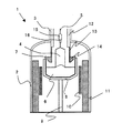
このうち、ルツボ底面部及び側面部に断熱材が配設された単結晶製造装置を図1に示す。この単結晶製造装置1は、ルツボ底面部及び側面部に断熱材17を配設した以外は、図2で示した単結晶製造装置とほとんど同じである。すなわち、ここでは、単結晶製造装置1のうち、メインチャンバー2内の、単結晶4、原料融液6、石英ルツボ7、黒鉛ルツボ8、シャフト9、黒鉛ヒーター10、断熱部材11、黒鉛筒13、断熱材14、そしてルツボの断熱材17を示している。これらのうち、特に、ルツボの断熱材17の数、大きさ、位置、素材等を変えて配設することによりTmax(℃)を所望範囲に変更することができる。
【0045】
また、Tmax(℃)は、ルツボサイズを変えることにより変更することもできる。例えば、ルツボのサイズをより小さくすれば、Tmax(℃)をより低くすることができ、したがって、図6に示すようにルツボサイズを小さくすることで所望欠陥領域及び/又は所望無欠陥領域を有するV/G値をより高く設定することができる。ルツボのサイズを、例えば、引上げる単結晶直径より大きく、かつ2.5倍以下の範囲にすることで、Tmax(℃)を十分に低くすることができ、したがって、所望欠陥領域及び/又は所望無欠陥領域を有するV/G値を十分に高い範囲に設定できる。
【0046】
以上のような本発明の単結晶の製造方法は、近年ますます単結晶製造装置が多様化し、所望欠陥領域及び/又は所望無欠陥領域を有するV/G値を正確に予想することが困難となっている上に、品質に対する要求が厳しいものとなっているシリコン単結晶を製造するのに、特に適している。
【0047】
さらに、本発明の単結晶の製造方法は、近年、需要が高まり、品質に対する要求も厳しくなっている直径200mm以上の単結晶を製造するのに、特に有効である。
【0048】
そして、このような本発明の単結晶の製造方法で製造された単結晶は、高品質なものである。
【0049】
【実施例】
以下、本発明を、実施例を挙げて具体的に説明する。
(実施例1)
図1に示したような単結晶製造装置(ルツボ口径600mm(24インチ))を用いて、直径8インチ(200mm)のシリコン単結晶を全面Cuデポ欠陥領域のないN領域となるように引上げることとした。
そのために、先ず、ルツボ底面部及び側面部に断熱材を配設し、ルツボと原料融液の界面での最高温度Tmax(℃)を、1514℃に設定した。このように設定したTmax(℃)から、Cuデポ欠陥領域のないN領域を有する単結晶を製造するためには、V/G値(mm2/K・min)の範囲を、0.21以上0.25以下(−0.000724×1514+1.31以上−0.000724×1514+1.35以下)の範囲にすれば良い(図3(c)参照。)。したがって、全面Cuデポ欠陥領域のないN領域となる単結晶を引上げるために、V/G値(mm2/K・min)の範囲を、安全を取って0.22以上0.24以下の範囲に決定した。次に、この決定したV/G値(mm2/K・min)の範囲に制御して単結晶を引上げた。すなわち、この単結晶製造装置AのHZでは、固液界面の温度勾配Gが、2.337K/mmであったため、引上げ速度Vを0.51mm/min以上0.56mm/min以下の範囲に制御して引上げた。
このようにして引上げたシリコン単結晶は、検査の結果、全面Cuデポ欠陥領域のないN領域であり、優れた品質のものであった。
【0050】
(実施例2)
実施例1と同様の単結晶製造装置を用いて、直径8インチ(200mm)のシリコン単結晶を全面Cuデポ欠陥領域のないN領域となるように引上げることとした。ただし、ルツボと原料融液の界面での最高温度Tmax(℃)を変更するための断熱材を設けなかった。
この単結晶製造装置は、ルツボと原料融液の界面での最高温度Tmax(℃)が1560℃であった。このTmax(℃)から、Cuデポ欠陥領域のないN領域を有する単結晶を製造するためには、V/G値(mm2/K・min)の範囲を、0.18以上0.22以下(−0.000724×1560+1.31以上−0.000724×1560+1.35以下)の範囲にすれば良い。したがって、全面Cuデポ欠陥領域のないN領域となる単結晶を引上げるために、V/G値(mm2/K・min)の範囲を、安全を見て、0.19以上0.21以下の範囲に決定した。次に、この決定したV/G値(mm2/K・min)の範囲に制御して単結晶を引上げた。すなわち、この単結晶製造装置のHZでは、固液界面の温度勾配Gが、2.500K/mmであったため、引上げ速度Vを0.48mm/min以上0.53mm/min以下の範囲に制御して引上げた。
このようにして引上げたシリコン単結晶は、検査の結果、全面Cuデポ欠陥領域のないN領域であり、優れた品質のものであった。
【0051】
(実施例3)
実施例1、2の単結晶製造装置とは異なる単結晶製造装置(ルツボの口径が750mm(30インチ))を用いて、直径8インチ(200mm)のシリコン単結晶を全面Cuデポ欠陥領域のないN領域となるように引上げることとした。
この単結晶製造装置は、ルツボと原料融液の界面での最高温度Tmax(℃)が1600℃であった。このTmax(℃)から、Cuデポ欠陥領域のないN領域を有する単結晶を製造するためには、V/G値(mm2/K・min)の範囲を、0.15以上0.19以下(−0.000724×1600+1.31以上−0.000724×1600+1.35以下)の範囲にすれば良い。したがって、全面Cuデポ欠陥領域のないN領域となる単結晶を引上げるために、V/G値(mm2/K・min)の範囲を、安全を見込んで、0.16以上0.18以下の範囲に決定した。次に、この決定したV/G値(mm2/K・min)の範囲に制御して単結晶を引上げた。すなわち、この単結晶製造装置のHZでは、固液界面の温度勾配Gが、2.674K/mmであったため、引上げ速度Vを0.43mm/min以上0.48mm/min以下の範囲に制御して引上げた。
このようにして引上げたシリコン単結晶は、検査の結果、全面Cuデポ欠陥領域のないN領域であり、優れた品質のものであった。
【0052】
(実施例4)
実施例1とほぼ同じ単結晶製造装置を用いて、直径8インチ(200mm)のシリコン単結晶を全面無欠陥領域ではなく、OSFリングを外方に排除して、結晶の径方向ほぼ全面がV領域となるように引上げることとした。ただし、ここで用いた単結晶製造装置は、原料融液6の表面と断熱材14の下端との距離が実施例1の単結晶製造装置と比較して半分の距離になるように断熱材14の位置を調節したものである。
この単結晶製造装置は、ルツボと原料融液の界面での最高温度Tmax(℃)が1514℃であった。このTmax(℃)から、結晶の径方向ほぼ全面がV領域を有する単結晶を製造するためには、V/G値(mm2/K・min)の範囲を、0.28以上(−0.000724×1514+1.38以上)の範囲にすれば良い。また、V/G値(mm2/K・min)は、単結晶が変形しないで育成できる範囲である1.90以下(−0.000724×1514+3.0以下)の範囲にする必要がある。したがって、結晶の径方向ほぼ全面がV領域を有する単結晶を引上げるために、V/G値(mm2/K・min)の範囲を、安全を見込んで、0.29以上0.31以下の範囲に決定した。次に、この決定したV/G値(mm2/K・min)の範囲に制御して単結晶を引上げた。すなわち、この単結晶製造装置のHZでは、固液界面の温度勾配の最大Gが、4.07K/mmであったため、引上げ速度Vを1.18mm/min以上1.26mm/min以下の範囲に制御して引上げた。
このようにして引上げたシリコン単結晶は、検査の結果、単結晶の径方向ほぼ全面で確実にOSFリングを排除したものとできることを確認できた。
【0053】
実施例1〜3から判るように、ルツボと原料融液界面での最高温度Tmax(℃)を、V/G値を決定する際のパラメーターとして用いることで、それぞれの単結晶製造装置に応じて、Cuデポ欠陥領域のないN領域を有するV/G値を正確に決定することができた。したがって、このように決定したV/G値に制御することで、Cuデポ欠陥領域のないN領域を有する単結晶を確実に引上げることができる。また、実施例1、2から判るように、断熱材を配設して、Tmax(℃)を低い温度に変更することで、Cuデポ欠陥領域のないN領域を有するV/G値を高くすることができた。したがって、引上げ速度Vを速めに設定することができ、単結晶の生産性を上げることができた。
【0054】
尚、本発明は、上記実施形態に限定されるものではない。上記実施形態は、例示であり、本発明の特許請求の範囲に記載された技術的思想と実質的に同一な構成を有し、同様な作用効果を奏するものは、いかなるものであっても本発明の技術的範囲に包含される。
【0055】
例えば本発明では窒素やカーボン等の不純物を添加しない場合(ノンドープ)の単結晶を製造する方法について説明したが、窒素やカーボンなどの不純物を添加する場合、V/G値がノンドープとは大きく異なるが、このような場合にも、Tmaxとは同様の関係にあり、それぞれの不純物、そしてそれらの濃度で変化する欠陥領域に対するV/G値に対してTmaxによる補正を加えることも、本発明の範囲に包含される。
【0056】
【発明の効果】
以上説明したように、本発明によれば、V/G値を制御して単結晶を引上げる際に、所望欠陥領域及び/又は所望無欠陥領域を有するV/G値をより正確に決定することができ、より確実に所望品質の単結晶を生産性よく引上げることができる。
【図面の簡単な説明】
【図1】ルツボ底面部及び側面部に断熱材が配設された単結晶製造装置の概略断面図である。
【図2】通常の単結晶製造装置の概略断面図である。
【図3】所望欠陥領域及び/又は無欠陥領域の単結晶となるV/G値とTmaxの範囲について示したグラフである。
(a)N領域及びOSF領域となるV/G値とTmaxの範囲、
(b)V領域となるV/G値とTmaxの範囲、
(c)Cuデポ欠陥領域のないN領域となるV/G値とTmaxの範囲。
【図4】Nv領域とNi領域の境界のV/G値とTmax(℃)の関係を示すグラフである。
【図5】成長速度と結晶の欠陥分布を示す説明図である。
【図6】Nv領域とNi領域の境界のV/G値とルツボ口径の関係を示すグラフである。
【符号の説明】
1…単結晶製造装置、 2…メインチャンバー、 3…引上げチャンバー、
4…単結晶、 5…ワイヤー、 6…原料融液、 7…石英ルツボ、
8…黒鉛ルツボ、 9…シャフト、 10…黒鉛ヒーター、
11…断熱部材、 12…冷却筒、 13…黒鉛筒、 14…断熱材、
15…種ホルダー、 16…種結晶、 17…断熱材。[0001]
BACKGROUND OF THE INVENTION
The present invention relates to a method for producing a single crystal by the Czochralski method, and more particularly to a method for producing a single crystal in a desired defect region and / or a desired defect-free region.
[0002]
[Prior art]
A single crystal used as a substrate of a semiconductor device is, for example, a silicon single crystal, and is mainly manufactured by a Czochralski method (hereinafter abbreviated as CZ method).
[0003]
When a single crystal is manufactured by the CZ method, for example, it is manufactured using a single
[0004]
The
[0005]
And the
[0006]
In addition, a
[0007]
The raw material polycrystal is accommodated in the
[0008]
Such a silicon single crystal manufactured by the CZ method is mainly used for manufacturing semiconductor devices. In recent years, semiconductor devices have been highly integrated and elements have been miniaturized. As device miniaturization advances, the problem of Grown-in crystal defects introduced during crystal growth becomes more important.
[0009]
Here, the Grown-in crystal defect will be described (see FIG. 5).
In a silicon single crystal, when the crystal growth rate is relatively high, a grown-in such as FPD (Flow Pattern Defect) or COP (Crystal Originated Particle) that is caused by voids in which hole-type point defects are gathered. Defects exist at high density throughout the crystal diameter direction, and a region where these defects exist is called a V (vacancy) region. In addition, when the growth rate is lowered, an OSF (Oxidation Induced Stacking Fault) region is generated in a ring shape from the periphery of the crystal as the growth rate is lowered, and when the growth rate is further lowered, the OSF ring is formed. Shrinks to the center of the wafer and disappears. On the other hand, when the growth rate is further reduced, defects such as LSEPD (Large Secco Etch Pit Defect) and LFPD (Large Flow Pattern Defect), which are considered to be caused by dislocation loops in which interstitial silicon has gathered, exist at low density. A region where a defect exists is called an I (Interstitial) region.
[0010]
In recent years, it has been discovered that there is an area outside the OSF ring between the V region and the I region where neither FPD, COP, etc. due to vacancies nor LSEPD, LFPD, etc. due to interstitial silicon exist. This region is called an N (neutral) region. Further, this N region is further classified into an Nv region (region with many vacancies) adjacent to the outside of the OSF ring and a Ni region (region with a lot of interstitial silicon) adjacent to the I region. In the Nv region, It is known that the amount of precipitated oxygen is large when the thermal oxidation treatment is performed, and there is almost no oxygen precipitation in the Ni region.
Furthermore, it can be seen that after the thermal oxidation treatment, there is a region (hereinafter referred to as a Cu deposition defect region) in which defects detected by the Cu deposition treatment are remarkably generated in a part of the Nv region where oxygen precipitation is likely to occur. It has been found that this causes deterioration of electrical characteristics such as oxide breakdown voltage characteristics.
[0011]
These Grown-in defects are considered to be determined by the parameter of V / G value, which is the ratio between the pulling rate (V) and the temperature gradient (G) at the solid-liquid interface (for example, (Refer
[0012]
For example, when pulling up the silicon single crystal, the V / G value is controlled to pull up the defect-free single crystal (see, for example, Patent Document 1), and the OSF ring or the nucleus in the OSF ring is formed in the plane. It has been disclosed to pull up a single crystal having gettering ability (see, for example, Patent Document 2). In addition, the V / G value is controlled, and nitrogen is further added to grow a silicon single crystal in the I region (see, for example, Patent Document 3). Similarly, nitrogen is added to determine the size of defects in the single crystal. Growing a single crystal having a uniform density and distribution (see, for example, Patent Document 4) is disclosed. From the single crystal thus manufactured, for example, an N region wafer in which the V region and the I region are excluded from the entire surface, a wafer in which the OSF is arranged on the outer periphery, an N region wafer having no Cu deposition defect region, etc. Can be manufactured.
[0013]
However, for example, when pulling up the single crystal of the N region over the entire surface, the defect distribution is actually investigated to obtain the V / G value having the region, and the single crystal is pulled up with the obtained V / G value. However, there have been many cases where the predicted V / G value is different from the V / G value at which a single crystal in the entire N region can actually be obtained. Particularly, in order to increase the pulling rate V and increase the productivity of the single crystal in the desired defect region and / or the desired defect-free region, the internal structure of the furnace (hot zone: HZ) so that the temperature gradient G at the solid-liquid interface increases. In spite of the setting, it has been found that a single crystal having a desired quality cannot be pulled unless the pulling speed V is actually made lower than the expected speed V. As described above, there is a problem that an accurate value of the V / G value having a desired defect region and / or a desired defect-free region is not clear and it is difficult to efficiently obtain a high-quality single crystal.
[0014]
[Patent Document 1]
JP-A-11-147786
[Patent Document 2]
JP 2000-44388 A
[Patent Document 3]
JP-A-11-349394
[Patent Document 4]
JP 2002-57160 A
[Non-Patent Document 1]
V. V. Voronkov, Journal of Crystal Growth, 59 (1982), 625-643
[0015]
[Problems to be solved by the invention]
The present invention has been made in view of such problems. When a single crystal is pulled by controlling the V / G value, the V / G having a desired defect region and / or a desired defect-free region can be more accurately detected. An object of the present invention is to provide a method for producing a single crystal capable of determining a value and capable of pulling a single crystal of a desired quality more reliably.
[0016]
[Means for Solving the Problems]
The present invention has been made to solve the above-described problems. In the method for producing a single crystal by pulling a seed crystal from a raw material melt by the Czochralski method, the pulling speed when pulling the single crystal is V ( mm / min), the temperature gradient at the solid-liquid interface is G (K / mm), and the maximum temperature at the interface between the crucible and the raw material melt is Tmax (° C.). And / or V / G value (mm2/ K · min) range is determined, and V / G (mm2/ K · min) is provided to provide a method for producing a single crystal characterized by pulling up the single crystal.
[0017]
Thus, the V / G value (mm) having a desired defect region and / or a desired defect-free region according to at least Tmax (° C.).2/ K · min) value is corrected to determine the range, and V / G (mm2V / G value (mm) having a desired defect region and / or a desired defect-free region by pulling up the single crystal by controlling the value of / K · min)2/ K · min) can be determined more accurately, so that a single crystal in a desired defect region and / or a defect-free region can be pulled more reliably. In addition to accurately predicting a V / G value having a desired defect region and / or a desired defect-free region according to various single crystal apparatuses, it is useful for designing a single crystal manufacturing apparatus. And thereby, the single crystal which has desired quality can be manufactured efficiently.
Here, the temperature gradient G (K / mm) at the solid-liquid interface refers to a temperature gradient in the range of the melting point of the raw material (1412 ° C. in the case of silicon) to 1400 ° C. Also, V / G value (mm2/ K · min) refers to control of the V / G value over almost the entire radial direction of the crystal (excluding the outer periphery of 0 to 2 cm because it is an outward diffusion region).
[0018]
In this case, the V / G value (mm2/ K · min) can be controlled within the range of −0.000724 × Tmax + 1.31 or more and less than −0.000724 × Tmax + 1.38 to pull up the single crystal..
[0019]
Thus, the V / G value (mm2/ K · min) is controlled in the range of −0.000724 × Tmax + 1.31 or more and less than −0.000724 × Tmax + 1.38, and the single crystal is pulled up, so that the N region and / or the OSF region is surely obtained. Single crystals can be produced.
More preferably, the V / G value (mm2/ K · min) is controlled in the range of −0.000724 × Tmax + 1.31 or more and −0.000724 × Tmax + 1.37 or less to pull up the single crystal, thereby reliably producing a single crystal having an N region. be able to.
[0020]
In this case, the V / G value (mm2/ K · min) can be controlled within the range of −0.000724 × Tmax + 1.38 or more to pull up the single crystal..
[0021]
Thus, the V / G value (mm2/ K · min) is controlled within a range of −0.000724 × Tmax + 1.38 or more to pull up the single crystal, whereby a single crystal in which the OSF ring is reliably removed outward can be manufactured.
[0022]
In this case, the V / G value (mm2/ K · min) can be controlled in the range of −0.000724 × Tmax + 1.31 or more and −0.000724 × Tmax + 1.35 or less to pull up the single crystal..
[0023]
Thus, the V / G value (mm2/ K · min) is controlled within the range of −0.000724 × Tmax + 1.31 or more and −0.000724 × Tmax + 1.35 or less to pull up the single crystal, thereby ensuring that the N region without the Cu deposit defect region is obtained. The single crystal which has can be manufactured.
[0024]
In this case, it is preferable to pull up the single crystal by setting the Tmax (° C.) to a range of 1560 ° C. or less..
[0025]
Thus, by setting Tmax (° C.) to a range of 1560 ° C. or less, the V / G value can be made sufficiently large. Therefore, the pulling speed V (mm / min) when pulling a single crystal having a desired defect region and / or a desired defect-free region can be sufficiently increased, and the productivity of the single crystal can be sufficiently increased.
[0026]
In this case, the Tmax (° C.) is set at least by providing a heat insulating material between the crucible containing the raw material melt and the heater arranged so as to surround the crucible, or arranging the heat insulating material on the bottom surface of the crucible. It can be changed by setting.
[0027]
Thus, by providing a heat insulating material at least between the crucible containing the raw material melt and the heater disposed so as to surround the crucible, or by disposing the heat insulating material on the bottom surface of the crucible, Tmax (° C.) can be changed to the desired temperature.
[0028]
In this case, the single crystal can be silicon..
[0029]
The single crystal manufacturing method of the present invention has been diversified in recent years, and it has become difficult to accurately determine a V / G value having a desired defect region and / or a desired defect-free region. It is particularly suitable for producing silicon single crystals that have strict quality requirements.
[0030]
In this case, the diameter of the single crystal can be 200 mm or more..
[0031]
The method for producing a single crystal according to the present invention is particularly effective for producing a single crystal having a diameter of 200 mm or more, which has recently been demanded and demands for quality have become severe.
[0032]
And the single crystal manufactured with such a manufacturing method of the single crystal of the present invention is of high quality..
[0033]
DETAILED DESCRIPTION OF THE INVENTION
Hereinafter, although embodiment of this invention is described, this invention is not limited to these.
As a result of diligent investigation using experiments and simulations, the present inventors have found that the predicted V / G value and the actual V / G value are different from each other, for example, single crystals having the same defect distribution. Examples of the difference between the expected pulling speed V and the actual pulling speed V for pulling up the single crystal in the desired defect region and / or the desired defect-free region are as follows. It has been found that when pulling a single crystal of a region and / or a desired defect-free region, the cause is that the V / G value having the region differs depending on each HZ. Therefore, if the present inventors can find a parameter that can be commonly used in various HZs, the parameter can be used to determine a more appropriate V / G value according to each HZ. As a result, the present invention has been completed.
[0034]
That is, the present invention relates to a method for producing a single crystal by pulling a seed crystal from a raw material melt by the Czochralski method, wherein the pulling speed when pulling the single crystal is V (mm / min), the solid-liquid interface (raw material When the temperature gradient of the melting point to 1400 ° C. is G (K / mm) and the maximum temperature at the interface between the crucible and the raw material melt is Tmax (° C.), the desired defect region and / or at least according to Tmax (° C.) Or V / G value (mm2/ K · min) range is determined, and V / G (mm2The method for producing a single crystal is characterized in that the value of / K · min) is controlled over almost the entire radial direction of the crystal (excluding the outer periphery of 0 to 2 cm) to pull up the single crystal.
[0035]
As described above, in the present invention, the maximum temperature Tmax (° C.) at the interface between the crucible and the raw material melt is used in addition to the V / G value as a parameter that can be commonly used in various HZs. This Tmax (° C.) can be obtained, for example, by measuring the temperature by placing thermocouples in increments of 2 cm from the bottom of the crucible toward the outer periphery, or can be obtained by calculation by simulation.
[0036]
Here, FIG. 4 is a graph showing the relationship between the V / G value at the boundary between the Nv region and the Ni region and Tmax (° C.). As apparent from FIG. 4, the V / G value and Tmax (° C.) have a clear correlation, and are extremely useful parameters in determining the V / G value having a desired defect region and / or a desired defect-free region. I know that there is. That is, in order to determine the V / G value to be controlled, correction by Tmax (° C.) is necessary.
[0037]
Accordingly, a V / G value (mm) having a desired defect region and / or a desired defect-free region according to at least Tmax (° C.).2/ K · min) range is determined, and V / G (mm2By pulling the single crystal by controlling the value of (/ K · min), the single crystal in the desired defect region and / or the desired defect-free region can be reliably pulled up. Further, a V / G value (mm) having a desired defect region and / or a desired defect-free region.2/ K · min) can be determined more accurately according to each of various HZs, so that a desired quality crystal can be efficiently obtained using any apparatus having HZ. This is also useful when designing a single crystal manufacturing apparatus.
[0038]
Therefore, FIG. 3 shows the results of a more detailed investigation on the range of V / G value and Tmax that become a single crystal of a desired defect region and / or a defect-free region. FIG. 3A is a graph showing the range of the V / G value and Tmax for the N region and the OSF region. FIG. 3B is a graph showing the range of the V / G value and Tmax that become the V region. Further, FIG. 3C is a graph showing the range of the V / G value and the Tmax that become the N region without the Cu deposit defect region.
[0039]
As is clear from FIG. 3A, the V / G value (mm2/ K · min) is controlled in the range of −0.000724 × Tmax + 1.31 or more and less than −0.000724 × Tmax + 1.38, and the single crystal is pulled up, so that the N region and / or the OSF region is surely obtained. Single crystals can be produced.
More preferably, the V / G value (mm2/ K · min) is controlled in the range of −0.000724 × Tmax + 1.31 or more and −0.000724 × Tmax + 1.37 or less to pull up the single crystal, thereby reliably producing a single crystal having an N region. be able to.
[0040]
Further, as apparent from FIG. 3B, the V / G value (mm2/ K · min) is controlled within a range of −0.000724 × Tmax + 1.38 or more to pull up the single crystal, whereby a single crystal in which the OSF ring is reliably removed outward can be manufactured.
[0041]
Further, as apparent from FIG. 3C, the V / G value (mm2/ K · min) is controlled within the range of −0.000724 × Tmax + 1.31 or more and −0.000724 × Tmax + 1.35 or less to pull up the single crystal, so that the N region having no Cu deposit defect region Can be produced.
[0042]
Further, as can be seen from FIGS. 3A to 3C, by setting Tmax (° C.) to a range of 1560 ° C. or less, a V / G value having a desired defect region and / or a desired non-defect region. (Mm2/ K · min) can be made sufficiently high. For example, from FIG. 3A and FIG. 3C, if Tmax (° C.) is 1560 ° C. or less, the V / G value (mm2It can be seen that / K · min) can be as high as 0.18 or more. Therefore, it becomes possible to produce a single crystal of desired quality with high productivity.
[0043]
The maximum temperature Tmax (° C.) at the interface between the crucible and the raw material melt can be changed by changing HZ.
For example, the desired range can be changed by providing a heat insulating material at least between the crucible containing the raw material melt and the heater arranged so as to surround the crucible, or by disposing a heat insulating material on the bottom surface of the crucible. can do.
[0044]
Among these, the single-crystal manufacturing apparatus with which the heat insulating material was arrange | positioned by the crucible bottom face part and side part is shown in FIG. This single
[0045]
Tmax (° C.) can also be changed by changing the crucible size. For example, if the size of the crucible is made smaller, Tmax (° C.) can be made lower. Therefore, as shown in FIG. 6, the crucible size is made smaller to have a desired defect region and / or a desired defect-free region. The V / G value can be set higher. By making the size of the crucible, for example, larger than the single crystal diameter to be pulled and within a range of 2.5 times or less, Tmax (° C.) can be made sufficiently low. The V / G value having a defect-free region can be set in a sufficiently high range.
[0046]
In the single crystal manufacturing method of the present invention as described above, single crystal manufacturing apparatuses are increasingly diversified in recent years, and it is difficult to accurately predict a V / G value having a desired defect region and / or a desired defect-free region. In addition, it is particularly suitable for producing silicon single crystals that have strict quality requirements.
[0047]
Furthermore, the method for producing a single crystal according to the present invention is particularly effective for producing a single crystal having a diameter of 200 mm or more, which has recently been demanded and demands for quality have become severe.
[0048]
And the single crystal manufactured with such a manufacturing method of the single crystal of this invention is a high quality thing.
[0049]
【Example】
Hereinafter, the present invention will be specifically described with reference to examples.
Example 1
Using a single crystal manufacturing apparatus (crucible diameter 600 mm (24 inches)) as shown in FIG. 1, a silicon single crystal having a diameter of 8 inches (200 mm) is pulled up so as to be an N region having no Cu deposit defect region. It was decided.
For this purpose, first, a heat insulating material was disposed on the bottom and side portions of the crucible, and the maximum temperature Tmax (° C.) at the interface between the crucible and the raw material melt was set to 1514 ° C. In order to manufacture a single crystal having an N region without a Cu deposition defect region from Tmax (° C.) set in this way, a V / G value (mm2/ K · min) may be in the range of 0.21 or more and 0.25 or less (−0.000724 × 1514 + 1.31 or more and −0.000724 × 1514 + 1.35 or less) (see FIG. 3C). .) Therefore, in order to pull up the single crystal that becomes the N region without the entire Cu deposition defect region, the V / G value (mm2/ K · min) was determined to be in the range of 0.22 to 0.24 for safety. Next, this determined V / G value (mm2/ K · min), the single crystal was pulled up. That is, in the HZ of this single crystal manufacturing apparatus A, the temperature gradient G at the solid-liquid interface was 2.337 K / mm, so the pulling speed V was 0.51 mm / min or more and 0.56 mm / min.Less thanPulled up to control the range.
As a result of the inspection, the silicon single crystal pulled in this way was an N region having no Cu deposit defect region on the entire surface, and was of excellent quality.
[0050]
(Example 2)
By using the same single crystal manufacturing apparatus as in Example 1, a silicon single crystal having a diameter of 8 inches (200 mm) was pulled up so as to be an N region having no Cu deposit defect region on the entire surface. However, a heat insulating material for changing the maximum temperature Tmax (° C.) at the interface between the crucible and the raw material melt was not provided.
In this single crystal manufacturing apparatus, the maximum temperature Tmax (° C.) at the interface between the crucible and the raw material melt was 1560 ° C. From this Tmax (° C.), in order to manufacture a single crystal having an N region without a Cu deposition defect region, a V / G value (mm2/ K · min) may be in the range of 0.18 to 0.22 (−0.000724 × 1560 + 1.31 to −0.000724 × 1560 + 1.35). Therefore, in order to pull up the single crystal that becomes the N region without the entire Cu deposition defect region, the V / G value (mm2The range of / K · min) was determined in the range of 0.19 to 0.21 in view of safety. Next, this determined V / G value (mm2/ K · min), the single crystal was pulled up. That is, in the HZ of this single crystal manufacturing apparatus, since the temperature gradient G at the solid-liquid interface was 2.500 K / mm, the pulling speed V was 0.48 mm / min or more and 0.53 mm / min.Less thanPulled up to control the range.
As a result of the inspection, the silicon single crystal pulled in this way was an N region having no Cu deposit defect region on the entire surface, and was of excellent quality.
[0051]
(Example 3)
Using a single crystal manufacturing apparatus (crucible diameter of 750 mm (30 inches)) different from the single crystal manufacturing apparatuses of Examples 1 and 2, a silicon single crystal having a diameter of 8 inches (200 mm) is entirely free from Cu deposition defects. It was decided to pull up so as to be in the N region.
In this single crystal manufacturing apparatus, the maximum temperature Tmax (° C.) at the interface between the crucible and the raw material melt was 1600 ° C. From this Tmax (° C.), in order to manufacture a single crystal having an N region without a Cu deposition defect region, a V / G value (mm2/ K · min) may be in the range of 0.15 or more and 0.19 or less (−0.000724 × 1600 + 1.31 or more and −0.000724 × 1600 + 1.35 or less). Therefore, in order to pull up the single crystal that becomes the N region without the entire Cu deposition defect region, the V / G value (mm2/ K · min) was determined to be in the range of 0.16 to 0.18 in consideration of safety. Next, this determined V / G value (mm2/ K · min), the single crystal was pulled up. That is, in the HZ of this single crystal manufacturing apparatus, the temperature gradient G at the solid-liquid interface was 2.674 K / mm, so the pulling speed V was 0.43 mm / min or more and 0.48 mm / min.Less thanPulled up to control the range.
As a result of the inspection, the silicon single crystal pulled in this way was an N region having no Cu deposit defect region on the entire surface, and was of excellent quality.
[0052]
Example 4
Using the same single crystal manufacturing apparatus as in Example 1, a silicon single crystal having a diameter of 8 inches (200 mm) was not entirely defect-free region, but the OSF ring was excluded outward, and almost the entire crystal radial direction was V. It was decided to pull it up to be an area. However, the single crystal manufacturing apparatus used here is such that the distance between the surface of the raw material melt 6 and the lower end of the
In this single crystal manufacturing apparatus, the maximum temperature Tmax (° C.) at the interface between the crucible and the raw material melt was 1514 ° C. From this Tmax (° C.), in order to produce a single crystal in which almost the entire radial direction of the crystal has a V region, a V / G value (mm2/ K · min) may be set to a range of 0.28 or more (−0.000724 × 1514 + 1.38 or more). Also, V / G value (mm2/ K · min) needs to be in the range of 1.90 or less (−0.000724 × 1514 + 3.0 or less), which is a range in which the single crystal can be grown without deformation. Therefore, in order to pull up a single crystal in which almost the entire radial direction of the crystal has a V region, V / G value (mm2/ K · min) was determined to be in a range of 0.29 to 0.31 in consideration of safety. Next, this determined V / G value (mm2/ K · min), the single crystal was pulled up. That is, in the HZ of this single crystal manufacturing apparatus, the maximum G of the temperature gradient at the solid-liquid interface was 4.07 K / mm, so the pulling speed V was in the range of 1.18 mm / min to 1.26 mm / min. Controlled and pulled up.
As a result of the inspection, it was confirmed that the silicon single crystal pulled up in this way can reliably eliminate the OSF ring almost over the entire radial direction of the single crystal.
[0053]
As can be seen from Examples 1 to 3, the maximum temperature Tmax (° C.) at the crucible and raw material melt interface is used as a parameter for determining the V / G value, and thus, according to each single crystal manufacturing apparatus. It was possible to accurately determine the V / G value having the N region without the Cu deposition defect region. Therefore, by controlling the V / G value determined in this way, it is possible to reliably pull up a single crystal having an N region without a Cu deposit defect region. Further, as can be seen from Examples 1 and 2, by providing a heat insulating material and changing Tmax (° C.) to a low temperature, the V / G value having an N region without a Cu deposit defect region is increased. I was able to. Therefore, the pulling speed V can be set higher and the productivity of the single crystal can be increased.
[0054]
The present invention is not limited to the above embodiment. The above-described embodiment is an exemplification, and the present invention has substantially the same configuration as the technical idea described in the claims of the present invention, and any device that exhibits the same function and effect is the present invention. It is included in the technical scope of the invention.
[0055]
For example, in the present invention, a method for producing a single crystal without adding impurities such as nitrogen and carbon (non-doped) has been described. However, when impurities such as nitrogen and carbon are added, the V / G value is significantly different from that of non-doped. However, even in such a case, Tmax has a similar relationship, and it is also possible to apply correction by Tmax to the V / G value for each impurity and a defect region that changes in their concentration. Included in the range.
[0056]
【The invention's effect】
As described above, according to the present invention, when pulling a single crystal by controlling a V / G value, a V / G value having a desired defect region and / or a desired defect-free region is more accurately determined. Therefore, a single crystal having a desired quality can be more reliably pulled out with high productivity.
[Brief description of the drawings]
FIG. 1 is a schematic cross-sectional view of a single crystal manufacturing apparatus in which a heat insulating material is disposed on a bottom surface portion and a side surface portion of a crucible.
FIG. 2 is a schematic cross-sectional view of a normal single crystal manufacturing apparatus.
FIG. 3 is a graph showing a range of V / G values and Tmax that are single crystals of a desired defect region and / or a defect-free region.
(A) V / G value and Tmax range for N region and OSF region,
(B) V / G value and Tmax range for the V region,
(C) A range of V / G value and Tmax that is an N region without a Cu deposit defect region.
FIG. 4 is a graph showing the relationship between the V / G value at the boundary between the Nv region and the Ni region and Tmax (° C.).
FIG. 5 is an explanatory diagram showing growth rate and crystal defect distribution;
FIG. 6 is a graph showing the relationship between the V / G value at the boundary between the Nv region and the Ni region and the crucible diameter.
[Explanation of symbols]
DESCRIPTION OF
4 ... single crystal, 5 ... wire, 6 ... raw material melt, 7 ... quartz crucible,
8 ... graphite crucible, 9 ... shaft, 10 ... graphite heater,
DESCRIPTION OF
15 ... Seed holder, 16 ... Seed crystal, 17 ... Insulating material.
Claims (5)
Priority Applications (6)
| Application Number | Priority Date | Filing Date | Title |
|---|---|---|---|
| JP2003135085A JP4151474B2 (en) | 2003-05-13 | 2003-05-13 | Method for producing single crystal and single crystal |
| KR1020057021320A KR101107653B1 (en) | 2003-05-13 | 2004-04-26 | Method for Producing Single Crystal and Single Crystal |
| US10/553,754 US7582159B2 (en) | 2003-05-13 | 2004-04-26 | Method for producing a single crystal |
| EP04729524.1A EP1624094B1 (en) | 2003-05-13 | 2004-04-26 | Method for producing single crystal |
| PCT/JP2004/006003 WO2004101868A1 (en) | 2003-05-13 | 2004-04-26 | Method for producing single crystal and single crystal |
| TW093112773A TW200500509A (en) | 2003-05-13 | 2004-05-06 | Method for producing single crystal and single crystal |
Applications Claiming Priority (1)
| Application Number | Priority Date | Filing Date | Title |
|---|---|---|---|
| JP2003135085A JP4151474B2 (en) | 2003-05-13 | 2003-05-13 | Method for producing single crystal and single crystal |
Publications (2)
| Publication Number | Publication Date |
|---|---|
| JP2004338979A JP2004338979A (en) | 2004-12-02 |
| JP4151474B2 true JP4151474B2 (en) | 2008-09-17 |
Family
ID=33447168
Family Applications (1)
| Application Number | Title | Priority Date | Filing Date |
|---|---|---|---|
| JP2003135085A Expired - Fee Related JP4151474B2 (en) | 2003-05-13 | 2003-05-13 | Method for producing single crystal and single crystal |
Country Status (6)
| Country | Link |
|---|---|
| US (1) | US7582159B2 (en) |
| EP (1) | EP1624094B1 (en) |
| JP (1) | JP4151474B2 (en) |
| KR (1) | KR101107653B1 (en) |
| TW (1) | TW200500509A (en) |
| WO (1) | WO2004101868A1 (en) |
Cited By (1)
| Publication number | Priority date | Publication date | Assignee | Title |
|---|---|---|---|---|
| JP7187335B2 (en) | 2019-01-25 | 2022-12-12 | 三菱重工サーマルシステムズ株式会社 | Air conditioner and method of operating the air conditioner |
Families Citing this family (9)
| Publication number | Priority date | Publication date | Assignee | Title |
|---|---|---|---|---|
| JP4710247B2 (en) * | 2004-05-19 | 2011-06-29 | 株式会社Sumco | Single crystal manufacturing apparatus and method |
| JP2006069841A (en) * | 2004-09-02 | 2006-03-16 | Sumco Corp | Magnetic field application method for pulling silicon single crystal |
| JP4513798B2 (en) * | 2006-10-24 | 2010-07-28 | 信越半導体株式会社 | Single crystal manufacturing apparatus and single crystal manufacturing method |
| JP5029184B2 (en) * | 2007-07-19 | 2012-09-19 | 日立電線株式会社 | Semiconductor crystal manufacturing method and manufacturing apparatus thereof |
| JP5151628B2 (en) * | 2008-04-02 | 2013-02-27 | 信越半導体株式会社 | Silicon single crystal wafer, silicon single crystal manufacturing method, and semiconductor device |
| JP2012142455A (en) * | 2010-12-29 | 2012-07-26 | Siltronic Ag | Method of manufacturing anneal wafer |
| CN102644104A (en) * | 2011-06-15 | 2012-08-22 | 安阳市凤凰光伏科技有限公司 | Gradient improving device of thermal field for producing pseudo single crystal silicon ingot by casting method |
| JP6107308B2 (en) * | 2013-03-28 | 2017-04-05 | 信越半導体株式会社 | Silicon single crystal manufacturing method |
| TWI771007B (en) * | 2020-05-19 | 2022-07-11 | 環球晶圓股份有限公司 | Method for producing si ingot single crystal, si ingot single crystal, and apparatus thereof |
Family Cites Families (41)
| Publication number | Priority date | Publication date | Assignee | Title |
|---|---|---|---|---|
| US3798007A (en) * | 1969-12-05 | 1974-03-19 | Ibm | Method and apparatus for producing large diameter monocrystals |
| US3653432A (en) * | 1970-09-01 | 1972-04-04 | Us Army | Apparatus and method for unidirectionally solidifying high temperature material |
| US3898051A (en) * | 1973-12-28 | 1975-08-05 | Crystal Syst | Crystal growing |
| US4108236A (en) * | 1977-04-21 | 1978-08-22 | United Technologies Corporation | Floating heat insulating baffle for directional solidification apparatus utilizing liquid coolant bath |
| US4178986A (en) * | 1978-03-31 | 1979-12-18 | General Electric Company | Furnace for directional solidification casting |
| US4196646A (en) * | 1978-05-13 | 1980-04-08 | Shigeyuki Mukumoto | Automatic meat arranging device for automatic meat cutting machine |
| US4202400A (en) * | 1978-09-22 | 1980-05-13 | General Electric Company | Directional solidification furnace |
| US4190094A (en) * | 1978-10-25 | 1980-02-26 | United Technologies Corporation | Rate controlled directional solidification method |
| DE3107596A1 (en) * | 1981-02-27 | 1982-10-21 | Heliotronic Forschungs- und Entwicklungsgesellschaft für Solarzellen-Grundstoffe mbH, 8263 Burghausen | "METHOD FOR PRODUCING SEMICONDUCTOR DISC" |
| US4409451A (en) * | 1981-08-31 | 1983-10-11 | United Technologies Corporation | Induction furnace having improved thermal profile |
| US4770704A (en) * | 1987-03-13 | 1988-09-13 | Iowa State University Research Foundation, Inc. | Continuous method for manufacturing grain-oriented magnetostrictive bodies |
| US4840699A (en) * | 1987-06-12 | 1989-06-20 | Ghemini Technologies | Gallium arsenide crystal growth |
| US5116456A (en) * | 1988-04-18 | 1992-05-26 | Solon Technologies, Inc. | Apparatus and method for growth of large single crystals in plate/slab form |
| US5134261A (en) * | 1990-03-30 | 1992-07-28 | The United States Of America As Represented By The Secretary Of The Air Force | Apparatus and method for controlling gradients in radio frequency heating |
| KR100246712B1 (en) * | 1994-06-02 | 2000-03-15 | 구마모토 마사히로 | Method and apparatus for preparing compound single crystals |
| FR2741633B1 (en) * | 1995-11-23 | 1997-12-19 | Commissariat Energie Atomique | CRYSTALLIZATION OVEN FOR MATERIAL WITH LOW THERMAL CONDUCTIVITY AND / OR LOW HARDNESS |
| JPH09263485A (en) | 1996-03-27 | 1997-10-07 | Nippon Steel Corp | Method for controlling pulling of single crystal, production of single crystal and apparatus therefor |
| JPH10152395A (en) * | 1996-11-21 | 1998-06-09 | Komatsu Electron Metals Co Ltd | Production of silicon single crystal |
| US5998257A (en) * | 1997-03-13 | 1999-12-07 | Micron Technology, Inc. | Semiconductor processing methods of forming integrated circuitry memory devices, methods of forming capacitor containers, methods of making electrical connection to circuit nodes and related integrated circuitry |
| CN101070621B (en) * | 1997-04-09 | 2012-09-05 | Memc电子材料有限公司 | Low defect density, self-interstitial dominated silicon |
| JPH10297994A (en) * | 1997-04-25 | 1998-11-10 | Sumitomo Sitix Corp | Growth of silicon single crystal |
| JP3460551B2 (en) * | 1997-11-11 | 2003-10-27 | 信越半導体株式会社 | Silicon single crystal wafer with few crystal defects and method of manufacturing the same |
| JP3747123B2 (en) * | 1997-11-21 | 2006-02-22 | 信越半導体株式会社 | Method for producing silicon single crystal with few crystal defects and silicon single crystal wafer |
| JPH11349394A (en) | 1998-06-04 | 1999-12-21 | Shin Etsu Handotai Co Ltd | Nitrogen-doped silicon single crystal wafer having low defect density and it production |
| JP3943717B2 (en) | 1998-06-11 | 2007-07-11 | 信越半導体株式会社 | Silicon single crystal wafer and manufacturing method thereof |
| JP2000034193A (en) * | 1998-07-16 | 2000-02-02 | Nikon Corp | Heat treatment and production of fluoride single crystal |
| JP4218080B2 (en) | 1998-07-30 | 2009-02-04 | 信越半導体株式会社 | Silicon single crystal wafer and manufacturing method thereof |
| US6312516B2 (en) * | 1998-10-14 | 2001-11-06 | Memc Electronic Materials, Inc. | Process for preparing defect free silicon crystals which allows for variability in process conditions |
| JP3601324B2 (en) * | 1998-11-19 | 2004-12-15 | 信越半導体株式会社 | Silicon single crystal wafer with few crystal defects and method of manufacturing the same |
| US6319313B1 (en) * | 1999-03-15 | 2001-11-20 | Memc Electronic Materials, Inc. | Barium doping of molten silicon for use in crystal growing process |
| US6673330B1 (en) * | 1999-03-26 | 2004-01-06 | National Institute For Research In Inorganic Materials | Single crystal of lithium niobate or tantalate and its optical element, and process and apparatus for producing an oxide single crystal |
| US6309461B1 (en) * | 1999-06-07 | 2001-10-30 | Sandia Corporation | Crystal growth and annealing method and apparatus |
| US6276432B1 (en) * | 1999-06-10 | 2001-08-21 | Howmet Research Corporation | Directional solidification method and apparatus |
| JP3783495B2 (en) * | 1999-11-30 | 2006-06-07 | 株式会社Sumco | Manufacturing method of high quality silicon single crystal |
| JP4463950B2 (en) | 2000-08-11 | 2010-05-19 | 信越半導体株式会社 | Method for manufacturing silicon wafer |
| JP3994665B2 (en) * | 2000-12-28 | 2007-10-24 | 信越半導体株式会社 | Silicon single crystal wafer and method for producing silicon single crystal |
| US6514337B2 (en) * | 2001-02-07 | 2003-02-04 | Seh America, Inc. | Method of growing large-diameter dislocation-free<110> crystalline ingots |
| JP2003002785A (en) * | 2001-06-15 | 2003-01-08 | Shin Etsu Handotai Co Ltd | Silicon single crystal wafer having layer free from void defect at surface layer part and diameter of not less than 300 mm, and method for producing the same |
| US6624390B1 (en) * | 2001-07-20 | 2003-09-23 | Cape Simulations, Inc. | Substantially-uniform-temperature annealing |
| JP2003204048A (en) * | 2002-01-09 | 2003-07-18 | Shin Etsu Handotai Co Ltd | Method for manufacturing soi wafer and soi wafer |
| US20030234092A1 (en) * | 2002-06-20 | 2003-12-25 | Brinegar John R. | Directional solidification method and apparatus |
-
2003
- 2003-05-13 JP JP2003135085A patent/JP4151474B2/en not_active Expired - Fee Related
-
2004
- 2004-04-26 EP EP04729524.1A patent/EP1624094B1/en not_active Expired - Fee Related
- 2004-04-26 WO PCT/JP2004/006003 patent/WO2004101868A1/en active Application Filing
- 2004-04-26 US US10/553,754 patent/US7582159B2/en active Active
- 2004-04-26 KR KR1020057021320A patent/KR101107653B1/en active IP Right Grant
- 2004-05-06 TW TW093112773A patent/TW200500509A/en unknown
Cited By (1)
| Publication number | Priority date | Publication date | Assignee | Title |
|---|---|---|---|---|
| JP7187335B2 (en) | 2019-01-25 | 2022-12-12 | 三菱重工サーマルシステムズ株式会社 | Air conditioner and method of operating the air conditioner |
Also Published As
| Publication number | Publication date |
|---|---|
| KR101107653B1 (en) | 2012-01-20 |
| TWI352136B (en) | 2011-11-11 |
| JP2004338979A (en) | 2004-12-02 |
| EP1624094A1 (en) | 2006-02-08 |
| KR20060003084A (en) | 2006-01-09 |
| EP1624094B1 (en) | 2013-10-02 |
| US20070000429A1 (en) | 2007-01-04 |
| WO2004101868A1 (en) | 2004-11-25 |
| EP1624094A4 (en) | 2011-04-13 |
| TW200500509A (en) | 2005-01-01 |
| US7582159B2 (en) | 2009-09-01 |
Similar Documents
| Publication | Publication Date | Title |
|---|---|---|
| KR101048831B1 (en) | Graphite heater for producing single crystal, single crystal manufacturing device and single crystal manufacturing method | |
| US7384477B2 (en) | Method for producing a single crystal and a single crystal | |
| JP4151474B2 (en) | Method for producing single crystal and single crystal | |
| US7226507B2 (en) | Method for producing single crystal and single crystal | |
| CN114318500A (en) | Crystal pulling furnace and method for pulling single crystal silicon rod and single crystal silicon rod | |
| US7323048B2 (en) | Method for producing a single crystal and a single crystal | |
| JP4457584B2 (en) | Method for producing single crystal and single crystal | |
| JP4207577B2 (en) | Method for producing P-doped silicon single crystal | |
| JP4496723B2 (en) | Single crystal manufacturing method and single crystal manufacturing apparatus | |
| KR20060093717A (en) | Process for producing single crystal | |
| JP2005015290A (en) | Method for manufacturing single crystal, and single crystal | |
| JP4218460B2 (en) | Graphite heater for single crystal production, single crystal production apparatus and single crystal production method | |
| JP4134800B2 (en) | Graphite heater for single crystal production, single crystal production apparatus and single crystal production method | |
| JP4148060B2 (en) | Graphite heater for single crystal production, single crystal production apparatus and single crystal production method | |
| JP4360208B2 (en) | Method for producing silicon single crystal | |
| JP4148059B2 (en) | Graphite heater for single crystal production, single crystal production apparatus and single crystal production method | |
| JPH11199383A (en) | Crystal growth | |
| JP4881539B2 (en) | Method for producing single crystal and single crystal | |
| KR100827033B1 (en) | Method of manufacturing defect-free single crystal and single crystal manufactured by using the same | |
| JP2005015298A (en) | Method for manufacturing single crystal, and single crystal | |
| JP2005015288A (en) | Method for manufacturing single crystal, and single crystal |
Legal Events
| Date | Code | Title | Description |
|---|---|---|---|
| A621 | Written request for application examination |
Free format text: JAPANESE INTERMEDIATE CODE: A621 Effective date: 20050117 |
|
| A131 | Notification of reasons for refusal |
Free format text: JAPANESE INTERMEDIATE CODE: A131 Effective date: 20080318 |
|
| A521 | Request for written amendment filed |
Free format text: JAPANESE INTERMEDIATE CODE: A523 Effective date: 20080430 |
|
| TRDD | Decision of grant or rejection written | ||
| A01 | Written decision to grant a patent or to grant a registration (utility model) |
Free format text: JAPANESE INTERMEDIATE CODE: A01 Effective date: 20080610 |
|
| A01 | Written decision to grant a patent or to grant a registration (utility model) |
Free format text: JAPANESE INTERMEDIATE CODE: A01 |
|
| A61 | First payment of annual fees (during grant procedure) |
Free format text: JAPANESE INTERMEDIATE CODE: A61 Effective date: 20080623 |
|
| R150 | Certificate of patent or registration of utility model |
Ref document number: 4151474 Country of ref document: JP Free format text: JAPANESE INTERMEDIATE CODE: R150 Free format text: JAPANESE INTERMEDIATE CODE: R150 |
|
| FPAY | Renewal fee payment (event date is renewal date of database) |
Free format text: PAYMENT UNTIL: 20110711 Year of fee payment: 3 |
|
| FPAY | Renewal fee payment (event date is renewal date of database) |
Free format text: PAYMENT UNTIL: 20110711 Year of fee payment: 3 |
|
| FPAY | Renewal fee payment (event date is renewal date of database) |
Free format text: PAYMENT UNTIL: 20120711 Year of fee payment: 4 |
|
| R250 | Receipt of annual fees |
Free format text: JAPANESE INTERMEDIATE CODE: R250 |
|
| FPAY | Renewal fee payment (event date is renewal date of database) |
Free format text: PAYMENT UNTIL: 20120711 Year of fee payment: 4 |
|
| FPAY | Renewal fee payment (event date is renewal date of database) |
Free format text: PAYMENT UNTIL: 20130711 Year of fee payment: 5 |
|
| R250 | Receipt of annual fees |
Free format text: JAPANESE INTERMEDIATE CODE: R250 |
|
| R250 | Receipt of annual fees |
Free format text: JAPANESE INTERMEDIATE CODE: R250 |
|
| R250 | Receipt of annual fees |
Free format text: JAPANESE INTERMEDIATE CODE: R250 |
|
| R250 | Receipt of annual fees |
Free format text: JAPANESE INTERMEDIATE CODE: R250 |
|
| S531 | Written request for registration of change of domicile |
Free format text: JAPANESE INTERMEDIATE CODE: R313531 |
|
| R350 | Written notification of registration of transfer |
Free format text: JAPANESE INTERMEDIATE CODE: R350 |
|
| R250 | Receipt of annual fees |
Free format text: JAPANESE INTERMEDIATE CODE: R250 |
|
| R250 | Receipt of annual fees |
Free format text: JAPANESE INTERMEDIATE CODE: R250 |
|
| R250 | Receipt of annual fees |
Free format text: JAPANESE INTERMEDIATE CODE: R250 |
|
| R250 | Receipt of annual fees |
Free format text: JAPANESE INTERMEDIATE CODE: R250 |
|
| R250 | Receipt of annual fees |
Free format text: JAPANESE INTERMEDIATE CODE: R250 |
|
| R250 | Receipt of annual fees |
Free format text: JAPANESE INTERMEDIATE CODE: R250 |
|
| LAPS | Cancellation because of no payment of annual fees |