JP4457584B2 - Method for producing single crystal and single crystal - Google Patents
Method for producing single crystal and single crystal Download PDFInfo
- Publication number
- JP4457584B2 JP4457584B2 JP2003185979A JP2003185979A JP4457584B2 JP 4457584 B2 JP4457584 B2 JP 4457584B2 JP 2003185979 A JP2003185979 A JP 2003185979A JP 2003185979 A JP2003185979 A JP 2003185979A JP 4457584 B2 JP4457584 B2 JP 4457584B2
- Authority
- JP
- Japan
- Prior art keywords
- single crystal
- pulling
- raw material
- crystal
- material melt
- Prior art date
- Legal status (The legal status is an assumption and is not a legal conclusion. Google has not performed a legal analysis and makes no representation as to the accuracy of the status listed.)
- Expired - Fee Related
Links
- 239000013078 crystal Substances 0.000 title claims description 462
- 238000004519 manufacturing process Methods 0.000 title claims description 39
- 239000002994 raw material Substances 0.000 claims description 117
- 230000007547 defect Effects 0.000 claims description 84
- XUIMIQQOPSSXEZ-UHFFFAOYSA-N Silicon Chemical compound [Si] XUIMIQQOPSSXEZ-UHFFFAOYSA-N 0.000 claims description 59
- 229910052710 silicon Inorganic materials 0.000 claims description 59
- 239000010703 silicon Substances 0.000 claims description 59
- 239000011261 inert gas Substances 0.000 claims description 30
- 238000000034 method Methods 0.000 claims description 21
- 239000007788 liquid Substances 0.000 claims description 8
- 239000000155 melt Substances 0.000 claims description 8
- 238000010438 heat treatment Methods 0.000 claims description 4
- 230000012010 growth Effects 0.000 description 39
- 239000007789 gas Substances 0.000 description 26
- 238000007689 inspection Methods 0.000 description 22
- XKRFYHLGVUSROY-UHFFFAOYSA-N Argon Chemical compound [Ar] XKRFYHLGVUSROY-UHFFFAOYSA-N 0.000 description 18
- 230000008021 deposition Effects 0.000 description 18
- 230000003247 decreasing effect Effects 0.000 description 12
- QVGXLLKOCUKJST-UHFFFAOYSA-N atomic oxygen Chemical compound [O] QVGXLLKOCUKJST-UHFFFAOYSA-N 0.000 description 11
- 239000001301 oxygen Substances 0.000 description 11
- 229910052760 oxygen Inorganic materials 0.000 description 11
- 230000000052 comparative effect Effects 0.000 description 10
- 230000007423 decrease Effects 0.000 description 10
- 230000020169 heat generation Effects 0.000 description 10
- 229910052786 argon Inorganic materials 0.000 description 9
- 238000001816 cooling Methods 0.000 description 7
- 238000000227 grinding Methods 0.000 description 7
- 239000010453 quartz Substances 0.000 description 7
- VYPSYNLAJGMNEJ-UHFFFAOYSA-N silicon dioxide Inorganic materials O=[Si]=O VYPSYNLAJGMNEJ-UHFFFAOYSA-N 0.000 description 7
- 238000004033 diameter control Methods 0.000 description 6
- 238000005498 polishing Methods 0.000 description 6
- 238000005520 cutting process Methods 0.000 description 5
- 238000002844 melting Methods 0.000 description 4
- 230000008018 melting Effects 0.000 description 4
- 230000004044 response Effects 0.000 description 4
- OKTJSMMVPCPJKN-UHFFFAOYSA-N Carbon Chemical compound [C] OKTJSMMVPCPJKN-UHFFFAOYSA-N 0.000 description 3
- 238000010586 diagram Methods 0.000 description 3
- 229910002804 graphite Inorganic materials 0.000 description 3
- 239000010439 graphite Substances 0.000 description 3
- 239000000463 material Substances 0.000 description 3
- 230000003647 oxidation Effects 0.000 description 3
- 238000007254 oxidation reaction Methods 0.000 description 3
- 239000004065 semiconductor Substances 0.000 description 3
- 238000004088 simulation Methods 0.000 description 3
- 238000009826 distribution Methods 0.000 description 2
- 230000000694 effects Effects 0.000 description 2
- 239000011810 insulating material Substances 0.000 description 2
- 229910021420 polycrystalline silicon Inorganic materials 0.000 description 2
- 238000001556 precipitation Methods 0.000 description 2
- 230000004043 responsiveness Effects 0.000 description 2
- 230000015556 catabolic process Effects 0.000 description 1
- 150000001875 compounds Chemical class 0.000 description 1
- 238000005137 deposition process Methods 0.000 description 1
- 230000006866 deterioration Effects 0.000 description 1
- 230000002542 deteriorative effect Effects 0.000 description 1
- 238000011156 evaluation Methods 0.000 description 1
- 238000002474 experimental method Methods 0.000 description 1
- 238000009413 insulation Methods 0.000 description 1
- 230000010354 integration Effects 0.000 description 1
- 230000021332 multicellular organism growth Effects 0.000 description 1
- 230000007935 neutral effect Effects 0.000 description 1
- 239000002245 particle Substances 0.000 description 1
- 230000005855 radiation Effects 0.000 description 1
- 238000003756 stirring Methods 0.000 description 1
- 239000000758 substrate Substances 0.000 description 1
- 239000003643 water by type Substances 0.000 description 1
Images


Landscapes
- Crystals, And After-Treatments Of Crystals (AREA)
Description
【0001】
【発明の属する技術分野】
本発明は、チョクラルスキー法による単結晶の製造方法に関し、特に所定の結晶直径及び所望の欠陥領域を有する単結晶を製造する方法に関する。
【0002】
【従来の技術】
半導体デバイスの基板として用いられる単結晶には、例えばシリコン単結晶等があり、主にチョクラルスキー法(Czochralski Method、以下CZ法と略称する)により製造されている。近年、半導体デバイスでは高集積化が促進され、素子の微細化が進んでいる。それに伴い、単結晶の結晶成長中に導入されるグローンイン(Grown−in)欠陥の問題がより重要となっている。
【0003】
ここで、グローンイン欠陥について図10を参照しながら説明する。
一般に、シリコン単結晶を成長させるときに、結晶成長速度V(結晶引上げ速度)が比較的高速の場合には、空孔型の点欠陥が集合したボイド起因とされているFPD(Flow Pattern Defect)やCOP(Crystal Originated Particle)等のグローンイン欠陥が結晶径方向全域に高密度に存在する。これらのボイド起因の欠陥が存在する領域はV(Vacancy)領域と呼ばれている。
【0004】
また、結晶成長速度を低くしていくと成長速度の低下に伴いOSF(酸化誘起積層欠陥、Oxidation Induced Stacking Fault)領域が結晶の周辺からリング状に発生し、さらに成長速度を低速にすると、OSFリングがウエーハの中心に収縮して消滅する。一方、さらに成長速度を低速にすると格子間シリコンが集合した転位ループ起因と考えられているLSEPD(Large Secco Etch Pit Defect)、LFPD(Large Flow Pattern Defect)等の欠陥が低密度に存在し、これらの欠陥が存在する領域はI(Interstitial)領域と呼ばれている。
【0005】
近年、V領域とI領域の中間でOSFリングの外側に、ボイド起因のFPD、COP等の欠陥も、格子間シリコン起因のLSEPD、LFPD等の欠陥も存在しない領域の存在が発見されている。この領域はN(ニュートラル、Neutral)領域と呼ばれる。また、このN領域をさらに分類すると、OSFリングの外側に隣接するNv領域(空孔の多い領域)とI領域に隣接するNi領域(格子間シリコンが多い領域)とがあり、Nv領域では、熱酸化処理をした際に酸素析出量が多く、Ni領域では酸素析出が殆ど無いことがわかっている。
【0006】
さらに、熱酸化処理後、酸素析出が発生し易いNv領域の一部に、Cuデポジション処理で検出される欠陥が著しく発生する領域(以下、Cuデポ欠陥領域という)があることが見出されており、これは酸化膜耐圧特性のような電気特性を劣化させる原因になることがわかっている。
【0007】
これらのグローンイン欠陥は、単結晶を成長させるときの引上げ速度V(mm/min)と固液界面近傍のシリコンの融点から1400℃の間の引上げ軸方向の結晶温度勾配G(℃/mm)の比であるV/G(mm2/℃・min)というパラメーターにより、その導入量が決定されると考えられている(例えば、非特許文献1参照)。すなわち、V/Gを所定の値で一定に制御しながら単結晶の育成を行うことにより、所望の欠陥領域あるいは所望の無欠陥領域を有する単結晶を製造することが可能となる。
【0008】
例えば特許文献1では、シリコン単結晶を育成する際に、結晶中心でV/G値を所定の範囲内(例えば、0.112〜0.142mm2/℃・min)に制御して単結晶を引上げることによって、ボイド起因の欠陥及び転位ループ起因の欠陥が存在しないシリコン単結晶ウエーハを得ることができることが示されている。また、近年では、Cuデポ欠陥領域を含まないN領域の無欠陥結晶に対する要求が高まりつつあり、V/Gを所定の無欠陥領域に高精度に制御しながら単結晶を引上げる単結晶の製造が要求されてきている。
【0009】
一般的に、引上げ軸方向の結晶温度勾配Gは、単結晶の育成が行われる単結晶引上げ装置のHZ(ホットゾーン:炉内構造)により一義的に決まるものとされていた。しかしながら、単結晶引上げ中にHZを変更することは極めて困難であることから、上記のようにV/Gを制御して単結晶の育成を行う場合、結晶温度勾配Gを単結晶引上げ中に制御することは行われず、引上げ速度Vを調節することによってV/G値を制御して所望の欠陥領域を有する単結晶を製造することが行われている。
【0010】
また、従来の単結晶の製造では、育成する単結晶の直径を制御するために、単結晶の引上げ速度を調節したり、原料融液を加熱するヒーターのパワーを変化させて原料融液の温度を調節することが行われている。しかしながら、上記のようにしてV/G値を制御して所望の欠陥領域を有する単結晶を育成する場合では、引上げ速度を調節することによりV/Gの制御を行うと同時に単結晶の直径制御も行われなければならないが、このとき結晶直径を所望の大きさにするために引上げ速度を大きく変化させてしまうと、引上げている単結晶の欠陥領域が変化してしまい単結晶を所望の欠陥領域で育成することができず、歩留まりの低下を招くといった問題があった。
【0011】
そこで従来は、このような問題を少しでも改善するために、結晶引上げ速度の変動を小さく抑えて単結晶を所望欠陥領域で育成できるようにするとともに、結晶直径を所望値に制御するためにヒーターパワーを変化させて原料融液の温度を調節することを行っていた。しかしながら、このようにして単結晶の育成を行っても、単結晶直胴部の全体を所定の直径で育成するとともに所望の欠陥領域を有するようにすることは非常に困難であり、またこのように結晶直径を制御するために原料融液の温度を調節する場合、単結晶の引上げ装置毎や単結晶の製造バッチ毎に原料融液の設定温度パターンを変更していかなければならなかった。そのため、単結晶引上げ装置毎や製造バッチ毎に温度パターンの合わせ込みを行わなければならず、直径を制御しながら所望の欠陥領域で単結晶を製造するためには大変な手間が必要とされ、作業における負担が非常に大きかった。
【0012】
【特許文献1】
特開平11−147786号公報
【非特許文献1】
V.V.Voronkov,Journal of CrystalGrowth,59(1982),625〜643
【0013】
【発明が解決しようとする課題】
そこで、本発明は上記問題点に鑑みてなされたものであって、本発明の目的は、CZ法により単結晶を育成する際に、単結晶の直径制御とV/Gの制御とを安定して行うことができ、所定の結晶直径と所望の欠陥領域を有する単結晶を容易にかつ高歩留まりで製造することのできる単結晶の製造方法を提供することにある。
【0014】
【課題を解決するための手段】
上記目的を達成するために、本発明によれば、チョクラルスキー法によりチャンバ内で単結晶を原料融液から引上げて製造する方法において、前記単結晶を育成する際に、前記単結晶の直胴部を成長させるときの引上げ速度をV(mm/min)、固液界面近傍の引上げ軸方向の結晶温度勾配をG(℃/mm)で表したとき、前記単結晶の直胴部の直径が所定値となるように前記引上げ速度Vを制御・変更しながら単結晶を引上げるとともに、該引上げ速度Vの変動に応じて前記結晶温度勾配Gを単結晶引上げ条件を変更することにより制御して、引上げ速度Vと結晶温度勾配Gの比V/G(mm2/℃・min)を所望の欠陥領域を有する単結晶が育成できるように制御することを特徴とする単結晶の製造方法が提供される。
【0015】
このように、CZ法によって単結晶を育成する際に、引上げ速度Vを制御・変更することにより結晶直径を安定して制御することができ、またそれと同時にVの変動に応じて他の単結晶引上げ条件を変更して結晶温度勾配Gを制御することにより、V/Gを所望の欠陥領域を有する単結晶が育成できるように安定して制御することができる。そして、このようにして直径制御とV/Gの制御とを行いながら単結晶を育成することによって、単結晶の直胴部全体に渡って所定の結晶直径を有し、かつ所望の欠陥領域を有する高品質の単結晶を容易にかつ高い歩留まりで製造することができる。
【0016】
このとき、前記単結晶を育成する際に変更する単結晶引上げ条件を、前記原料融液の融液面と前記チャンバ内で原料融液面に対向配置された遮熱部材との距離、前記単結晶を引上げる際の単結晶の回転速度、前記原料融液を収容するルツボの回転速度、前記チャンバに導入する不活性ガスの流量、前記原料融液を加熱するヒーターの位置、前記チャンバ内の圧力、前記原料融液に印加する磁場の磁場強度、及び前記原料融液面と原料融液に印加する磁場の磁場中心との相対距離のうちの少なくとも1つとすることが好ましい。
【0017】
このように、単結晶を育成する際に、上記に示した単結晶引上げ条件のうちの少なくとも1つを変更することによって、引上げ速度Vの変動に応じて結晶温度勾配Gを容易に制御することが可能となり、それによってV/Gを所望欠陥領域を有する単結晶が育成できるように高精度に安定して制御することができる。
【0018】
この場合、前記V/Gを、前記育成する単結晶の欠陥領域が径方向の全面にわたってN領域となるように制御することが好ましい。
このように、V/Gを単結晶の欠陥領域が径方向全面でN領域となるように制御することによって、単結晶直胴部においてFPDやCOP等のボイド起因の欠陥も、またLSEPD、LFPD等の転位ループ起因の欠陥も存在せず、かつ結晶直径も高精度に制御された非常に高品質の単結晶を高歩留まりで製造することができる。
【0019】
また、前記単結晶の直胴部の直径を、200mm以上とすることができる。
本発明の単結晶の製造方法は、直径が200mm以上となる大口径の単結晶を製造する場合にも非常に有効に適用することができ、従来では製造が困難であった単結晶直胴部の全域で所望の欠陥領域となる直径200mm以上の大口径の単結晶を容易にかつ非常に安定して製造することができる。
【0020】
さらに、前記製造する単結晶をシリコン単結晶とすることができる。
このように、本発明の単結晶の製造方法は、シリコン単結晶を製造する場合に特に好適に用いることができ、本発明によりシリコン単結晶を製造することによって、シリコン単結晶の育成中に直径の制御とV/Gの制御とを安定して行うことが可能となり、直胴部全体に渡って所定の結晶直径を有し、かつ所望の欠陥領域を有する高品質のシリコン単結晶を簡便にかつ高い歩留まりで製造することができる。
【0021】
そして、本発明によれば、前記単結晶の製造方法により製造された単結晶が提供される。
本発明により製造された単結晶は、単結晶直胴部全域に渡って所定の結晶直径を均一に有し、かつ所望の欠陥領域を有する非常に高品質の単結晶とすることができる。
【0022】
【発明の実施の形態】
以下、本発明について実施の形態を説明するが、本発明はこれらに限定されるものではない。
本発明者等は、CZ法により所定の結晶直径を有するとともに所望の欠陥領域を有する単結晶を容易にかつ高歩留まりで製造できる方法について検討を重ね、単結晶を引上げる際に引上げ速度Vを制御・変更することにより直径の制御を行い、また一方で固液界面近傍のシリコンの融点から1400℃の間の引上げ軸方向の結晶温度勾配Gを単結晶引上げ中に制御することができれば、直径制御のため引上げ速度Vを大きく変動させてもV/Gの制御が可能となり、所定の結晶直径及び所望の欠陥領域を有する単結晶を高歩留まりで簡便に育成することができると考えた。
【0023】
そこで、本発明者等はさらに実験及び検討を重ねた結果、CZ法により単結晶を育成する際の原料融液の融液面と原料融液面に対向するように配置された遮熱部材との距離、単結晶を回転させる単結晶の回転速度、原料融液を収容しているルツボの回転速度、チャンバに導入する不活性ガスの流量、原料融液を加熱するヒーターの位置、チャンバ内の圧力、原料融液に印加する磁場の磁場強度、及び原料融液面と原料融液に印加する磁場の磁場中心との相対距離といった単結晶引上げ条件に注目し、これらの各単結晶引上げ条件を単結晶引上げ中に故意に変化させることによって固液界面近傍のシリコンの融点から1400℃の間の引上げ軸方向の結晶温度勾配Gを制御することができることを見出し、単結晶引上げ中に直径制御のために引上げ速度Vを変動させても結晶温度勾配Gを変更・制御することによってV/Gを所望欠陥領域に高精度に制御できることがわかった。
【0024】
また、本発明者等は総合伝熱解析ソフトFEMAG(F.Dupret, P.Nicodeme, Y.Ryckmans, P.Wouters, and M.J.Crochet, Int.J.Heat Mass Transfer,33,1849(1990))を用いて、単結晶を育成する際に上記に示した各単結晶引上げ条件を変化させた場合の結晶温度勾配Gの変化についてシミュレーション解析を行った。図1〜図8に、単結晶の引上げ中に原料融液面と遮熱部材間の距離L1を変化させた場合のGの変化、単結晶の回転速度を変化させた場合のGの変化、ルツボの回転速度を変化させた場合のGの変化、不活性ガスの流量を変化させた場合のGの変化、ヒーターの位置を変化させた場合のヒーターの発熱中心位置と原料融液面との相対距離L2に対するGの変化、チャンバ内の圧力を変化させた場合のGの変化、原料融液に印加する磁場強度を変化させた場合のGの変化、原料融液面と原料融液に印加する磁場の磁場中心との相対距離L3を変化させた場合のGの変化についてそれぞれシミュレーション解析した結果の一例を示す。
【0025】
図1〜図8に示したように、シミュレーション解析の結果、上記に示した各引上げ条件を変化させることによって結晶温度勾配Gが変化することが明らかとなり、例えば単結晶引上げ中に、原料融液面と遮熱部材間の距離L1を減少させる、単結晶の回転速度を速くする、ルツボの回転速度を遅くする、不活性ガスの流量を増加させる、ヒーターの発熱中心位置と原料融液面との相対距離L2が大きくなるようにヒーターの位置を変化させる、チャンバ内の圧力を低下させる、磁場強度を強める、または原料融液面と磁場中心との相対距離L3を減少させることによって結晶温度勾配Gを大きくすることができ、また一方、それぞれの単結晶引上げ条件を上記と増減を反対にして変化させることによって結晶温度勾配Gを小さくできることがわかった。
【0026】
さらに、単結晶引上げ中に上記の各単結晶引上げ条件を変化させたときの結晶温度勾配Gが変化するまでの時間(応答性)について調査したところ、単結晶の引上げ中に原料融液面と遮熱部材間の距離L1、単結晶の回転速度、不活性ガスの流量を変化させた場合には、それらの引上げ条件の変化に応じて結晶温度勾配Gもすぐに変化して迅速な応答性を示すことが明らかとなり、比較的短周期の引上げ速度Vの変動に対して結晶温度勾配Gを制御する際に非常に好適であることがわかった。また、ルツボの回転速度、ヒーターの位置、チャンバ内の圧力、磁場強度、原料融液面と磁場中心との相対距離L3を変化させた場合には、結晶温度勾配Gは緩やかに変化するため、比較的長周期の引上げ速度Vの変動に対して結晶温度勾配Gを制御する際に好適であることがわかった。そして、これらを組合せて制御すれば、引上げ速度Vの種々の変動に対して高精度でV/Gを所定値内に制御することができることが判った。
【0027】
本発明は、上記のような単結晶引上げ中の単結晶引上げ条件と結晶温度勾配Gとの関係を利用することにより、単結晶を育成する際に単結晶の直径制御とV/Gの制御を非常に安定して行うことができるようにしたものである。
すなわち、本発明の単結晶の製造方法は、CZ法によって単結晶を育成する際に、単結晶直胴部の直径が所定値となるように引上げ速度Vを制御・変更しながら単結晶を引上げるとともに、その引上げ速度Vの変動に応じて結晶温度勾配Gを単結晶引上げ条件を変更することにより制御して、所望の欠陥領域を有する単結晶が育成できるようにV/Gを所望値に制御することに特徴を有するものである。
【0028】
以下、本発明の単結晶の製造方法について図面を参照しながら詳細に説明するが、本発明はこれに限定されるものではない。
本発明の単結晶の製造方法で用いられる単結晶引上げ装置は、単結晶の引上げ中に原料融液面と遮熱部材間の距離L1、単結晶の回転速度、ルツボの回転速度、不活性ガスの流量、ヒーターの位置、チャンバ内の圧力、原料融液に印加する磁場の磁場強度、原料融液面と原料融液に印加する磁場の磁場中心との相対距離L3のうちの少なくとも一つの単結晶引上げ条件を変更できるものであれば特に限定されないが、例えば図9に示すような単結晶引上げ装置を用いることができる。先ず、図9を参照しながら、本発明の単結晶の製造方法を実施する際に使用することのできる単結晶引上げ装置について説明する。
【0029】
図9に示した単結晶引上げ装置20は、メインチャンバ1内に、原料融液4を収容する石英ルツボ5と、この石英ルツボ5を保護する黒鉛ルツボ6とがルツボ駆動機構21によって回転・昇降自在に保持軸13で支持されており、またこれらのルツボ5、6を取り囲むように加熱ヒーター7と断熱材8が配置され、さらに加熱ヒーター7の位置を調節できるようにヒーター駆動手段22が設けられている。
【0030】
メインチャンバ1の上部には育成した単結晶3を収容し、取り出すための引上げチャンバ2が連接されており、引上げチャンバ2の上部には単結晶3をワイヤー14で回転させながら引上げる引上げ機構17が設けられている。
【0031】
さらに、メインチャンバ1の内部にはガス整流筒11が設けられており、このガス整流筒11の下部には原料融液4と対向するように遮熱部材12を設置して、原料融液4の表面からの輻射をカットするとともに原料融液4の表面を保温するようにしている。また、ガス整流筒11の上部には、ガス整流筒11を昇降させて遮熱部材12の位置を上下に調整できる遮熱部材駆動手段23が設置されている。尚、本発明において、遮熱部材12の形状や材質等は特に限定されるものではなく、必要に応じて適宜変更することができる。さらに、本発明の遮熱部材12は、融液面に対向配置されたものであれば良く、必ずしも上記のようにガス整流筒の下部に設置されているものに限定されない。
【0032】
また、引上げチャンバ2の上部に設けられたガス導入口10からはバルブ24で流量を調節しながらアルゴンガス等の不活性ガスを導入でき、引上げ中の単結晶3とガス整流筒11との間を通過させた後、遮熱部材12と原料融液4の融液面との間を通過させ、ガス流出口9から排出することができる。さらに、ガス流出口9は真空ポンプ(不図示)に接続されており、バルブ26を調節することによってメインチャンバ1及び引上げチャンバ2内の圧力を調節できるようになっている。
【0033】
さらに、メインチャンバ1の外側には原料融液4に磁場を所望の磁場強度で印加することができる超伝導マグネットからなる磁場発生装置25が設置されており、さらに磁場発生装置25の位置を上下に調節できるように磁場発生装置駆動手段27が設けられている。
【0034】
そして、上記の引上げ機構17、ルツボ駆動機構21、ヒーター駆動手段22、遮熱部材駆動手段23、バルブ24,26、磁場発生装置25、及び磁場発生装置駆動手段27はそれぞれ引上げ条件制御手段18に接続されており、この引上げ条件制御手段18に、例えばCCDカメラ19で測定した原料融液面の位置及び単結晶3の直径や、遮熱部材12の位置、単結晶3の回転速度、ルツボ5,6の位置及び回転速度、不活性ガスの流量、加熱ヒーター7の位置、磁場発生装置25から原料融液4に印加している磁場の磁場強度や磁場中心、チャンバ内に設けられた圧力計(不図示)で測定したチャンバ内の圧力、さらに引上げ機構17から得られる単結晶の引上げ長さ等の情報がフィードバックされることにより、引上げ機構17、ルツボ駆動機構21、ヒーター駆動手段22、遮熱部材駆動手段23、バルブ24,26、磁場発生装置25、及び磁場発生装置駆動手段27を引上げ条件制御手段18でそれぞれ調節して、単結晶の引上げ中に原料融液面と遮熱部材間の距離L1、単結晶の回転速度、ルツボの回転速度、不活性ガスの流量、ヒーターの位置、チャンバ内の圧力、磁場強度、原料融液面と磁場中心との相対距離L3等をそれぞれ精度良く制御・変更することができるようになっている。
【0035】
尚、本発明で使用することのできる単結晶引上げ装置は、上記に示した装置に限定されるものではなく、その他にガス整流筒11の代わりに単結晶3を冷却する冷却ジャケットを設置したり、さらに冷却ジャケットの先端に吸熱フィンを設けたりすることも可能である。
【0036】
このような単結晶引上げ装置20を用いて、CZ法により例えばシリコン単結晶を育成する場合、ガス導入口10から引上げチャンバ2及びメインチャンバ1に不活性ガス(例えば、アルゴンガス)を導入しながら、種ホルダー15に固定された種結晶16を石英ルツボ5中の原料融液4に浸漬し、その後回転させながら静かに引上げて種絞りを形成した後結晶直径が所定の値、例えば200mm以上となるまで拡径し、略円柱形状の直胴部を有するシリコン単結晶3を成長させることができる。
【0037】
本発明は、このようにしてシリコン単結晶3の直胴部を成長させる際に、単結晶の直胴部の直径が所定値となるように引上げ速度Vを制御・変更しながら単結晶3を引上げるとともに、その引上げ速度Vの変動に応じて原料融液面と遮熱部材間の距離L1、単結晶3の回転速度、ルツボ5,6の回転速度、チャンバに導入する不活性ガスの流量、加熱ヒーター7の位置、チャンバ内の圧力、磁場強度、原料融液面と磁場中心との相対距離L3のうちの少なくとも1つの単結晶引上げ条件を変更することによって、固液界面近傍の引上げ軸方向の結晶温度勾配Gを制御することができる。そしてそれによって、育成する単結晶の直径制御を高精度に行うことができるとともにV/Gの制御も非常に安定して行うことができるので、所定の結晶直径及び所望の欠陥領域を有する高品質の単結晶を容易にかつ安定して育成することができる。
【0038】
以下、具体的に説明すると、例えばシリコン単結晶を欠陥領域が径方向の全面にわたってN領域となるように育成する場合、前述のように種絞りを形成してから直径が所定値となるまで拡径した後、単結晶の直胴部をN領域で育成できるように引上げ速度Vを単結晶の製造が行われる製造環境(例えば、単結晶引上げ装置のHZ等)に応じて調節する。
【0039】
そして、単結晶直胴部の直径を成長させる際には、単結晶直胴部の直径が所定値で維持されるように引上げ速度Vを制御・変更するとともに、その引上げ速度Vの変動に応じて原料融液面と遮熱部材間の距離L1、単結晶の回転速度、ルツボの回転速度、チャンバに導入する不活性ガスの流量、加熱ヒーターの位置、チャンバ内の圧力、磁場強度、原料融液面と磁場中心との相対距離L3のうちの少なくとも1つの単結晶引上げ条件を変更することによって結晶温度勾配Gを制御する。このとき、結晶温度勾配Gを変化させることができる他の因子を同時に制御・変更しても良い。
【0040】
例えば、直胴部の直径を所定値で維持するために引上げ速度を速くした場合、引上げ速度Vの増加に応じて結晶温度勾配Gを大きくするために、原料融液面と遮熱部材間の距離L1を減少させる、引上げ機構17により単結晶の回転速度を速くする、ルツボ駆動機構21によりルツボ5,6の回転速度を遅くする、バルブ24を開いてチャンバに導入する不活性ガスの流量を増加させる、加熱ヒーター7の発熱中心位置と原料融液面との相対距離L2が大きくなるように加熱ヒーター7の位置をヒーター駆動手段22によって変更する(ヒーターの位置を下げる)、バルブ26を調節してチャンバ内の圧力を低下させる、磁場発生装置25で原料融液に印加する磁場の磁場強度を大きくする、及び原料融液面と原料融液に印加する磁場の磁場中心との相対距離L3を減少させるといった各単結晶引上げ条件の変更のうちの少なくとも1つを行う。
【0041】
尚、原料融液面と遮熱部材間の距離L1は、ルツボ駆動機構21で石英ルツボ5及び黒鉛ルツボ6を結晶成長による融液面低下分とは異なる速度で押し上げることによって原料融液面の高さを結晶成長軸方向で上昇・下降させたり、また遮熱部材駆動手段23でガス整流筒11を昇降させて遮熱部材12の位置を上下に移動させたりすることによって容易にかつ高精度で変更させることができる。また原料融液面と原料融液に印加する磁場の磁場中心との相対距離L3は、原料融液面の高さを上記と同様にして結晶成長軸方向で上昇・下降させたり、また磁場発生装置駆動手段27で磁場発生装置25の位置を上下に移動させたりすることによって、容易にかつ高精度で変更させることができる。さらに、上記では、原料融液面の位置よりヒーター発熱中心及び磁場中心が下となる場合を例として説明しているが、もちろんヒーター発熱中心や磁場中心を融液面より上となるように制御することも可能である。
【0042】
また一方、直胴部の直径を制御するために引上げ速度を遅くした場合では、引上げ速度Vの減少に応じて結晶温度勾配Gを小さくするために、原料融液面と遮熱部材間の距離L1を増大させる、単結晶の回転速度を遅くする、ルツボの回転速度を速くする、不活性ガスの流量を減少させる、加熱ヒーターの発熱中心位置と原料融液面との相対距離L2が小さくなるように加熱ヒーター7の位置を上昇させる、チャンバ内の圧力を高める、磁場強度を小さくする、及び原料融液面と磁場中心との相対距離L3を増大させるといった各単結晶引上げ条件の変更のうちの少なくとも1つを行う。
【0043】
尚、前述したように、上記に示した単結晶引上げ条件のうち、原料融液面と遮熱部材間の距離L1、単結晶の回転速度、不活性ガスの流量については、それらを変化させたときに結晶温度勾配Gもすぐに変化して素早い応答性を示し、また、ルツボの回転速度、加熱ヒーターの位置、チャンバ内の圧力、磁場強度、原料融液面と磁場中心との相対距離L3は、結晶温度勾配Gを緩やかに変化させる。さらに、磁場強度、及び原料融液面と磁場中心との相対距離L3については、例えば上記磁場発生装置25で磁場強度を調節したり、また磁場発生装置駆動手段27で磁場発生装置25の位置を上下に調節した際に、実際に原料融液に印加している磁場の磁場強度や磁場中心が所望されたように変化するまでに若干の時間が必要となる場合がある。
【0044】
したがって、上記のような各単結晶引上げ条件の特徴を考慮すると、例えばGの応答性が優れている原料融液面と遮熱部材間の距離L1、単結晶の回転速度、不活性ガスの流量は比較的短い周期の引上げ速度Vの変動に対して変更することが好ましく、例えば数分程度の比較的短い時間で引上げ速度Vの平均を求め、その短時間の引上げ速度の平均値の変動に基づいて原料融液面と遮熱部材間の距離L1、単結晶の回転速度、不活性ガスの流量を変更することによって、V/Gの制御を高精度に行うことができる。
【0045】
また、Gを緩やかに変化させるルツボの回転速度、加熱ヒーターの位置、チャンバ内の圧力は短周期から長周期の引上げ速度の変動に対して変更することが好ましく、例えば数分〜数十分程度の比較的長時間で求めた引上げ速度の平均値の変動に基づいてそれらの引上げ条件を変更することによって結晶温度勾配Gの制御を行えば良い。さらに磁場強度、及び原料融液面と磁場中心との相対距離L3を変更する場合であれば、Gの変化が緩やかであるとともに、実際に原料融液に印加される磁場強度や磁場中心が変化するまでには時間がかかるために、引上げ速度の平均値を例えば5分以上の非常に長い時間で求めて、その引上げ速度の平均値の変動、つまり長周期の引上げ速度Vの変動に基づいて磁場強度、及び原料融液面と磁場中心との相対距離L3を変更することが好ましい。このように変更する単結晶引上げ条件によって異なる時間間隔で引上げ速度の平均値を求め、その求めた引上げ速度の平均値の変動に基づいて各単結晶引上げ条件を変更することによって、様々な周期の引上げ速度の変動に応じて結晶温度勾配Gを精度良く制御することが可能となり、それによりV/Gの制御を非常に高精度に行って、所望の欠陥領域で単結晶を安定して育成することができる。
【0046】
さらに、本発明では、単結晶を育成する際に、引上げ速度Vの変動に応じて上記に示した単結晶引上げ条件のうちの2つ以上の条件を変更することによって、結晶温度勾配Gの制御を行うこともできる。通常、上記の各単結晶引上げ条件は、単結晶を育成する際に結晶品質等その他の様々な製造条件にも作用している。そのため、単結晶の製造環境によっては、一つの引上げ条件のみを大きく変更すると種々の不都合が生じることが懸念される場合がある。例えば、原料融液面と遮熱部材間の距離L1を大きく広げ過ぎたり、不活性ガスの流量を増加させ過ぎたりすると単結晶育成の際の操業性が悪化する場合があったり、さらに単結晶の回転速度やルツボの回転速度が余りに速くなり過ぎたり、また遅くなり過ぎたりすると単結晶直胴部の形状が変形したり、結晶面内の品質分布の悪化が生じて歩留まりの低下を招くといった不都合が生じる可能性があることが考えられる。
【0047】
しかしながら、上記のように単結晶を育成する際に、単結晶引上げ条件のうちの2つ以上の条件を変更することによって、1つの引上げ条件を変更させるときに比べて結晶温度勾配Gをより広範囲で制御することができるようになるし、また引上げ条件の変更による結晶温度勾配Gの制御精度や応答性も向上させることができるようになる。また、例えば結晶温度勾配Gを大きくする場合には原料融液面と遮熱部材間の距離L1を縮小させ、一方結晶温度勾配Gを小さくする場合には不活性ガスの流量を減少させるといったようにすれば、操業性を悪化させず、またその他の様々な製造条件への影響を小さくして結晶温度勾配Gの制御を行うことが可能となる。さらに、例えば原料融液面と遮熱部材間の距離L1等のような比較的短い周期の引上げ速度の変動に対して変更する単結晶引上げ条件と、短周期から長周期の引上げ速度の変動や長周期の引上げ速度の変動に対して変更する単結晶引上げ条件と組み合わせて単結晶引上げ中に変更すれば、様々な引上げ速度Vの変動に対して結晶温度勾配Gを一層高精度に制御することが可能となり、所望の欠陥領域を有する単結晶を非常に安定して製造することができる。
【0048】
尚、本発明は、単結晶育成中に原料融液面と遮熱部材間の距離L1、単結晶の回転速度、ルツボの回転速度、不活性ガスの流量、加熱ヒーターの位置、チャンバ内の圧力、磁場強度、原料融液面と磁場中心との相対距離L3のうちの少なくとも1つを変更すれば良く、実際に単結晶の製造が行われる製造環境(例えばHZの構造)等に応じて、変更させる引上げ条件の数やパラメータを適宜選択することができる。また、上記以外の因子を同時に制御・変更するようにすることも可能である。
【0049】
また、上記引上げ条件を変更する際の各引上げ条件の制御範囲についても、単結晶の製造環境等に応じて適宜決定することができ、特に限定されるものではないが、例えば単結晶育成中に1つの引上げ条件を過剰に変更させ過ぎてしまうと上記に示したような不都合を生じる恐れがある。したがって、単結晶引上げ中は、各単結晶引上げ条件を単結晶が安定して育成することができる範囲で変更することが好ましい。
【0050】
例えば、単結晶育成中に原料融液面と遮熱部材間の距離L1を変更する場合は、引上げる単結晶の直径にもよるが、距離L1を1〜500mm、好ましくは10〜300mm、さらに好ましくは20〜200mmの範囲で変更することが望ましく、以下同様に、単結晶の回転速度の場合は0.1〜40rpm、好ましくは5〜20rpmの範囲で変更し、ルツボの回転速度の場合は0.1〜40rpmの範囲で変更し、不活性ガスの流量の場合は10〜2000L/min、好ましくは60〜300L/minの範囲で変更し、加熱ヒーターの位置については加熱ヒーターの発熱中心位置と原料融液面との相対距離L2が0〜500mm、好ましくは10〜200mm、さらに好ましくは30〜100mmの範囲で変化するようにヒーター位置を変更し、チャンバ内の圧力の場合は5〜300mbar、好ましくは10〜200mbarの範囲で変更し、磁場強度は100〜10000G、好ましくは500〜6000Gの範囲で変更し、原料融液面と磁場中心との相対距離L3の場合は0〜1000mm、好ましくは5〜500mmの範囲で変更することが望ましい。
【0051】
さらに、本発明では、図9に示した引上げ条件制御手段18を用いることにより、単結晶の引上げ中に単結晶の直径が所定値となるように引上げ速度Vを自動的に制御・変更するとともに、引上げ速度Vの変動に応じて結晶温度勾配Gも自動的に制御することが可能となる。具体的に説明すると、例えば単結晶引上げ中に、CCDカメラ19で測定した原料融液面の位置及び単結晶3の直径や、遮熱部材12の位置、単結晶3の回転速度、ルツボ5,6の位置及び回転速度、不活性ガスの流量、加熱ヒーター7の位置、磁場発生装置25から原料融液4に印加している磁場の磁場強度や磁場中心、チャンバ内の圧力、さらに引上げ機構17から得られる単結晶の引上げ長さ等の情報を引上げ条件制御手段18にフィードバックすることによって、引上げ条件制御手段18で引上げ機構17の駆動を調節して単結晶3が所定の直径で育成できるように引上げ速度Vを自動的に制御・変更する。そして、このように引上げ速度Vを制御・変更すると同時に、変更した引上げ速度Vの変動に応じて引上げ条件制御手段18で引上げ機構17、ルツボ駆動機構21、ヒーター駆動手段22、遮熱部材駆動手段23、バルブ24,26、磁場発生装置25、及び磁場発生装置駆動手段27を調節して、原料融液面と遮熱部材間の距離L1、単結晶の回転速度、ルツボの回転速度、チャンバに導入する不活性ガスの流量、加熱ヒーターの位置、チャンバ内の圧力、磁場強度、原料融液面と磁場中心との相対距離L3のうちの少なくとも1つ変更するようにすれば、結晶温度勾配Gを自動的に制御してV/Gを所望欠陥領域を有する単結晶が育成できるように高精度に制御することができる。
【0052】
このように、本発明によれば、単結晶引上げ中に単結晶直胴部の直径が所定値となるように引上げ速度Vを制御・変更するとともに、その引上げ速度Vの変動に応じて原料融液面と遮熱部材間の距離L1、単結晶の回転速度、ルツボの回転速度、チャンバに導入する不活性ガスの流量、加熱ヒーターの位置、チャンバ内の圧力、磁場強度、原料融液面と磁場中心との相対距離L3のうちの少なくとも1つを変更して結晶温度勾配Gを制御することにより、V/Gを所望の欠陥領域を有する単結晶が育成できるように安定して制御することができる。したがって、従来のように単結晶引上げ装置毎や製造バッチ毎に温度パターンの合わせ込み等を行わなくても、単結晶引上げ中に単結晶の直径制御とV/Gの制御とを安定して行うことができるため、例えば直径が200mm以上となる大口径の単結晶であっても、単結晶の直胴部全体に渡って所定の結晶直径を有し、かつ所望の欠陥領域を有する非常に高品質の単結晶を従来よりも非常に簡便にかつ高い歩留まりで製造することができる。
【0053】
さらに、単結晶を育成する際に本発明のように引上げ速度Vの変動に応じて結晶温度勾配Gを制御することによって、V/Gの制御性を向上させることができる。そのため、例えば図10に示すような、Cuデポ欠陥領域を含まないN領域中のNv領域やNi領域といった狭い領域にV/Gを高精度に制御して単結晶を製造することが可能となり、所望の欠陥領域を有する高品質の単結晶を非常に安定して得ることができる。
【0054】
尚、本発明では、前述のようにガス整流筒11の代わりに単結晶3を冷却する冷却ジャケットを設置したり、さらに冷却ジャケットの先端に吸熱フィンを設けたりすることも可能であり、その場合、引上げ速度Vの変動に応じて原料融液面と冷却ジャケット間の距離、また原料融液面と吸熱フィン間の距離を変更することによって、V/Gを所望の欠陥領域を有する単結晶が育成できるように制御することも可能となる。
【0055】
【実施例】
以下、実施例及び比較例を示して本発明をより具体的に説明するが、本発明はこれらに限定されるものではない。
(実施例1:原料融液面と遮熱部材間の距離L1の変更)
図9に示した単結晶引き上げ装置20を用いて、CZ法により直径24インチ(600mm)の石英ルツボに原料多結晶シリコンを150kgチャージし、ガス導入口10からアルゴンガスを流しながら、方位<100>、直径200mm、酸素濃度が22〜23ppma(ASTM’79)となるシリコン単結晶をCuデポジション欠陥が検出されないN領域で育成した(単結晶直胴部の長さは約100cm)。
【0056】
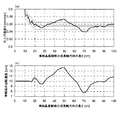
また、シリコン単結晶の直胴部を育成している間は、CCDカメラ19で単結晶直胴部の直径を測定し、その情報を引上げ条件制御手段18にフィードバックして引上げ機構17を調節することによって、シリコン単結晶の直胴部の直径が200mmとなるように引上げ速度Vの制御・変更を行った。またそれと同時に、引上げ速度Vの変動に応じて原料融液面と遮熱部材間の距離L1を変更するために、2分間の引上げ速度の平均値を求め、その引上げ速度の平均値が0.02mm/min増加した場合には原料融液面と遮熱部材間の距離L1が5mm縮小するような割合で、また引上げ速度の平均値が0.02mm/min減少した場合には距離L1が5mm拡大するような割合で引上げ条件制御手段18でルツボ駆動機構21及び遮熱部材駆動手段23を調節した。
【0057】
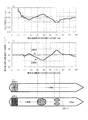
このようにして単結晶育成中に変化させた引上げ速度V及び原料融液面と遮熱部材間の距離L1の変化の割合をそれぞれ図11の(a)、(b)に示す。尚、図11(a)に示したように、直胴部10cm以内の範囲で引上げ速度が高速であるのは、拡径部から直胴部に入るためのいわゆる肩部の引上げであるためで、肩部を形成することで直胴部の引上げに移行し、直胴部の直径を安定して制御することが可能となる。
【0058】
次に、上記のようにして育成した単結晶の成長軸方向の各部位から検査用のウエーハを切り出した後、平面研削及び研磨を行って検査用のサンプルを作製し、以下に示すような結晶品質特性の検査を行った。
【0059】
(1)FPD(V領域)及びLSEPD(I領域)の検査
検査用のサンプルに30分間のセコエッチングを無攪拌で施した後、ウエーハ面内を顕微鏡で観察することにより結晶欠陥の有無を確認した。
(2)OSFの検査
検査用のサンプルにウエット酸素雰囲気下、1100℃で100分間の熱処理を行った後、ウエーハ面内を顕微鏡で観察することによりOSFの有無を確認した。
(3)Cuデポジション処理による欠陥の検査
検査用のサンプルの表面に酸化膜を形成した後、Cuデポジション処理を行って酸化膜欠陥の有無を確認した。その際の評価条件は以下の通りである。
酸化膜:25nm
電解強度:6MV/cm
電圧印加時間:5分間
【0060】
(比較例)
上記実施例と同様の単結晶引上げ装置20を用いて、直径24インチ(600mm)の石英ルツボに原料多結晶シリコンを150kgチャージし、CZ法により、方位<100>、直径200mm、酸素濃度が22〜23ppma(ASTM’79)となるシリコン単結晶をCuデポジション欠陥が検出されないN領域で育成した(単結晶直胴部の長さは約100cm)。
【0061】
また、シリコン単結晶の直胴部を育成している間は、CCDカメラ19で単結晶直胴部の直径を測定して引上げ条件制御手段18で引上げ機構17を調節することによって、シリコン単結晶の直胴部の直径が200mmとなるように引上げ速度Vの制御・変更を行った。尚、このときの引上げ速度Vの変化の割合は上記実施例1とほぼ同様であった。一方、その他の単結晶引上げ条件については、単結晶直胴部の引上げ中に常に一定となるようにした。
【0062】
この比較例における引上げ速度Vの変化の割合を図11(a)に重ねて示し(実施例1の引上げ速度Vとほぼ同じ値)、また実施例1と比較するために比較例における単結晶直胴部育成中の原料融液面と遮熱部材間の距離L1の値(単結晶育成中は一定)を図11(b)に示す。
そして、上記で得られた単結晶の成長軸方向の各部位から検査用のウエーハを切り出した後、平面研削及び研磨を行って検査用のサンプルを作製し、実施例1と同様の結晶品質特性の検査を行った。
【0063】
上記のようにして実施例1及び比較例で作製したシリコン単結晶にそれぞれ結晶品質特性の検査を行った結果、実施例1で作製したシリコン単結晶には単結晶直胴部10cmから直胴部終端までの領域において、FPD、LSEPD、OSFの何れの欠陥も検出されず、またCuデポジション処理による欠陥も観察されなかった。したがって、実施例1のシリコン単結晶は、単結晶直胴部の直胴部10cm以内の範囲を除く全ての領域において、Cuデポジション欠陥が検出されないN領域となっていることが確認できた。
【0064】
それに対して、比較例で作製したシリコン単結晶では、引上げ速度Vが大きく変動した直胴部の40〜55cmの領域でOSFが観察され、また直胴部の65〜75cmの領域ではLSEPD(I領域)が観察された。ここで、実施例1及び比較例で作製したシリコン単結晶に結晶品質特性の検査を行った結果を比較しやすくするために、それぞれの単結晶の欠陥領域を模式的に示した図を図11(c)に示す。
【0065】
(実施例2:単結晶の回転速度の変更、実施例3:不活性ガスの流量の変更)
図9に示した単結晶引き上げ装置20を用いて、上記実施例1と同様にしてCZ法により、方位<100>、直径200mm、酸素濃度が22〜23ppma(ASTM’79)となるシリコン単結晶をCuデポジション欠陥が検出されないN領域で育成した(単結晶直胴部の長さは約100cm)。
【0066】
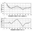
また、シリコン単結晶の直胴部を育成している間、実施例2では、上記実施例1と同様にシリコン単結晶の直胴部の直径が200mmとなるように引上げ速度Vの制御・変更を行うとともに、引上げ速度Vの変動に応じて単結晶の回転速度を変更するために、2分間の引上げ速度の平均値を求め、その引上げ速度の平均値が0.02mm/min増加した場合には単結晶の回転速度が3.0rpm速くなるような割合で、また引上げ速度の平均値が0.02mm/min減少した場合には単結晶の回転速度が3.0rpm遅くなるような割合で引上げ条件制御手段18で引上げ機構17を調節した。
【0067】
さらに、実施例3では、シリコン単結晶の直胴部の直径が200mmとなるように引上げ速度Vの制御・変更を行うとともに、引上げ速度Vの変動に応じて不活性ガス(アルゴンガス)の流量を変更するために、2分間の引上げ速度の平均値が0.02mm/min増加した場合にはアルゴンガスの流量が50L/min増加するような割合で、また引上げ速度の平均値が0.02mm/min減少した場合にはアルゴンガスの流量が50L/min減少するような割合で引上げ条件制御手段18でバルブ24を調節した。
【0068】
ここで、実施例2において上記のようにして単結晶育成中に変化させた引上げ速度V及び単結晶の回転速度の変化の割合をそれぞれ図12の(a)、(b)に示し、また実施例3において単結晶育成中に変化させた引上げ速度V及びアルゴンガスの流量の変化の割合をそれぞれ図13の(a)、(b)に示す。
【0069】
そして、上記実施例2及び実施例3のそれぞれで得られた単結晶の成長軸方向の各部位から検査用のウエーハを切り出した後、平面研削及び研磨を行って検査用のサンプルを作製し、実施例1と同様の結晶品質特性の検査を行った。その結果、実施例2及び実施例3で作製した両シリコン単結晶とも、単結晶直胴部の直胴部10cm以内の範囲を除く全ての領域において、Cuデポジション欠陥が検出されないN領域となっていることが確認できた。
【0070】
(実施例4:ルツボの回転速度の変更、実施例5:チャンバ内の圧力の変更)
図9に示した単結晶引き上げ装置20を用いて、上記実施例1と同様にしてCZ法により、方位<100>、直径200mm、酸素濃度が22〜23ppma(ASTM’79)となるシリコン単結晶をCuデポジション欠陥が検出されないN領域で育成した(単結晶直胴部の長さは約100cm)。
【0071】
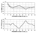
また、シリコン単結晶の直胴部を育成している間、実施例4では、上記実施例1と同様にシリコン単結晶の直胴部の直径が200mmとなるように引上げ速度Vの制御・変更を行うとともに、引上げ速度Vの変動に応じてルツボの回転速度を変更するために、10分間の引上げ速度の平均値を求め、その引上げ速度の平均値が0.01mm/min増加した場合にはルツボの回転速度が0.5rpm遅くなるような割合で、また引上げ速度の平均値が0.01mm/min減少した場合にはルツボの回転速度が0.5rpm速くなるような割合で引上げ条件制御手段18でルツボ駆動機構21を調節した。
【0072】
さらに、実施例5では、シリコン単結晶の直胴部の直径が200mmとなるように引上げ速度Vの制御・変更を行うとともに、引上げ速度Vの変動に応じてチャンバ内の圧力を変更するために、10分間の引上げ速度の平均値が0.01mm/min増加した場合にはチャンバ内の圧力が25mbar低下させるような割合で、また引上げ速度の平均値が0.01mm/min減少した場合にはチャンバ内の圧力が25mbar高まるような割合で引上げ条件制御手段18でバルブ26を調節した。
【0073】
ここで、実施例4において上記のようにして単結晶育成中に変化させた引上げ速度V及びルツボの回転速度の変化の割合をそれぞれ図14の(a)、(b)に示し、また実施例5において単結晶育成中に変化させた引上げ速度V及びチャンバ内の圧力の変化の割合をそれぞれ図15の(a)、(b)に示す。
【0074】
そして、上記実施例4及び実施例5のそれぞれで得られた単結晶の成長軸方向の各部位から検査用のウエーハを切り出した後、平面研削及び研磨を行って検査用のサンプルを作製し、実施例1と同様の結晶品質特性の検査を行った。その結果、実施例4及び実施例5で作製した両シリコン単結晶とも、一部の極わずかな結晶部位で結晶欠陥が観察されたものの、単結晶直胴部の直胴部10cm以内の範囲を除く95%以上の領域で、Cuデポジション欠陥が検出されないN領域となっていることがわかった。したがって、実施例4及び実施例5のシリコン単結晶は、上記の比較例や従来行われていた単結晶の引上げ装置毎や単結晶の製造バッチ毎に原料融液の設定温度パターンを変更して所定の結晶直径で単結晶を製造する方法と比較しても、同等以上の歩留まりを確保できることが確認できた。
【0075】
尚、実施例4及び実施例5のシリコン単結晶の一部で結晶欠陥が観察された原因としては、ルツボの回転速度やチャンバ内の圧力を引上げ速度の変動に応じて変更しても、実際に結晶温度勾配Gが変化するまでに多少のタイムラグが生じたためと考えられる。
【0076】
(実施例6:原料融液面と遮熱部材間の距離L1及び不活性ガスの流量の変更)図9に示した単結晶引き上げ装置20を用いて、上記実施例1と同様にしてCZ法により、方位<100>、直径200mm、酸素濃度が22〜23ppma(ASTM’79)となるシリコン単結晶をCuデポジション欠陥が検出されないN領域で育成した(単結晶直胴部の長さは約100cm)。
【0077】
また、シリコン単結晶の直胴部を育成している間、上記実施例1と同様にシリコン単結晶の直胴部の直径が200mmとなるように引上げ速度Vの制御・変更を行うとともに、2分間の引上げ速度の平均値を求めて、その引上げ速度の平均値が0.02mm/min増加した場合には原料融液面と遮熱部材間の距離L1が5mm縮小するような割合で引上げ条件制御手段18でルツボ駆動機構21を調節し、一方引上げ速度の平均値が0.02mm/min減少した場合にはアルゴンガスの流量が50L/min減少するような割合で引上げ条件制御手段18でバルブ24を調節した。
【0078】
そして、得られた単結晶の成長軸方向の各部位から検査用のウエーハを切り出した後、平面研削及び研磨を行って検査用のサンプルを作製し、実施例1と同様の結晶品質特性の検査を行った。その結果、実施例6で作製したシリコン単結晶は、単結晶直胴部の直胴部10cm以内の範囲を除く全ての領域において、Cuデポジション欠陥が検出されないN領域となっていることが確認できた。
【0079】
(実施例7)
図9に示した単結晶引き上げ装置20とは遮熱部材の形状及び材質の異なる別の単結晶引き上げ装置を用いて、CZ法により、方位<100>、直径200mm、酸素濃度が22〜23ppma(ASTM’79)となるシリコン単結晶をCuデポジション欠陥が検出されないN領域で複数バッチ連続して育成した(単結晶直胴部の長さは約100cm)。
【0080】
尚、シリコン単結晶を複数バッチ連続して製造する際、各製造バッチで単結晶直胴部を育成するときに、上記実施例6と同様に単結晶の直径が200mmとなるように引上げ速度Vの制御・変更を行うとともに、その引上げ速度の変動に応じて原料融液面と遮熱部材間の距離L1及び不活性ガスの流量を変更した。
【0081】
そして、連続して得られた複数の単結晶について実施例1と同様の結晶品質特性の検査を各単結晶に行った結果、全てのシリコン単結晶が、単結晶直胴部の直胴部10cm以内の範囲を除く全ての領域において、Cuデポジション欠陥が検出されないN領域となっていることが確認できた。
【0082】
(実施例8:加熱ヒーターの位置の変更)
図9に示した単結晶引き上げ装置20を用いて、上記実施例1と同様にしてCZ法により、方位<100>、直径200mm、酸素濃度が22〜23ppma(ASTM’79)となるシリコン単結晶をCuデポジション欠陥が検出されないN領域で育成した(単結晶直胴部の長さは約100cm)。
【0083】
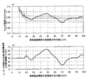
また、シリコン単結晶の直胴部を育成している間、実施例8では、上記実施例1と同様にシリコン単結晶の直胴部の直径が200mmとなるように引上げ速度Vの制御・変更を行うとともに、引上げ速度Vの変動に応じて加熱ヒーターの位置を変更するために、10分間の引上げ速度の平均値を求め、その引上げ速度の平均値が0.01mm/min増加した場合には加熱ヒーターの発熱中心位置と原料融液面との相対距離L2が15mm大きくなるような割合で、また引上げ速度の平均値が0.01mm/min減少した場合には加熱ヒーターの発熱中心位置と原料融液面との相対距離L2が15mm小さくなるような割合で引上げ条件制御手段18でヒーター駆動手段22を調節して加熱ヒーターの位置を変更した。
【0084】
ここで、実施例8において上記のようにして単結晶育成中に変化させた引上げ速度V及び加熱ヒーターの発熱中心位置と原料融液面との相対距離L2の変化の割合をそれぞれ図16の(a)、(b)に示す。
【0085】
そして、上記実施例8で得られた単結晶の成長軸方向の各部位から検査用のウエーハを切り出した後、平面研削及び研磨を行って検査用のサンプルを作製し、実施例1と同様の結晶品質特性の検査を行った。その結果、実施例8で作製したシリコン単結晶は、一部の極わずかな結晶部位で結晶欠陥が観察されたものの、単結晶直胴部の直胴部10cm以内の範囲を除く95%以上の領域で、Cuデポジション欠陥が検出されないN領域となっていることがわかった。したがって、実施例8のシリコン単結晶は、上記の比較例や従来行われていた単結晶の引上げ装置毎や単結晶の製造バッチ毎に原料融液の設定温度パターンを変更して所定の結晶直径で単結晶を製造する方法と比較しても、同等以上の歩留まりを確保できることが確認できた。
【0086】
尚、実施例8のシリコン単結晶の一部で結晶欠陥が観察された原因としては、加熱ヒーターの位置を引上げ速度の変動に応じて変更しても、実際に結晶温度勾配Gが変化するまでに多少のタイムラグが生じたためと考えられる。
【0087】
なお、本発明は、上記実施形態に限定されるものではない。上記実施形態は、例示であり、本発明の特許請求の範囲に記載された技術的思想と実質的に同一な構成を有し、同様な作用効果を奏するものは、いかなるものであっても本発明の技術的範囲に包含される。
【0088】
例えば、上記実施の形態では単結晶をN領域で育成する場合を例に挙げて説明を行っているが、本発明はこれに限定されず、V領域またはI領域、あるいはOSF領域といった所望の欠陥領域で単結晶を育成することもできる。また、本発明は、シリコン単結晶を製造する場合に好適に用いることができるが、これに限定されるものではなく、化合物半導体単結晶等を製造する場合にも同様に適用することができる。さらに、本発明は、磁場を原料融液に印加せずに単結晶を育成する場合や、磁場及び電流を原料融液に印加しながら単結晶を育成する場合(EMCZ法)にも同様に適用できる。
【0089】
尚、本発明の単結晶の製造方法は、必ずしも単結晶直胴部の全長で実施する場合に限られず、一部の長さに渡って引上げ速度Vで直径制御を行うとともに、その引上げ速度Vの変動に応じて結晶温度勾配Gを制御して、所望の欠陥領域とする場合を含む。特に上記のように、直胴部の前半である肩部から10cmの領域は、結晶品質が安定しないことがあるので、これが定常状態となり易い直胴部の5cm以降あるいは10cm以降で行うのが好ましい。
【0090】
【発明の効果】
以上説明したように、本発明によれば、単結晶を育成する際に、引上げ速度Vを制御・変更することにより結晶直径を安定して制御することができ、またそれと同時に引上げ速度Vの変動に応じて単結晶引上げ条件を変更して結晶温度勾配Gを制御することにより、V/Gを所望の欠陥領域を有する単結晶が育成できるように安定して制御することができる。そして、このようにして直径制御とV/Gの制御とを行いながら単結晶を育成することによって、単結晶の直胴部全体に渡って所定の結晶直径を有し、かつ所望の欠陥領域を有する高品質の単結晶を容易にかつ高い歩留まりで製造することができる。
【図面の簡単な説明】
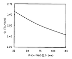
【図1】原料融液面と遮熱部材間の距離L1と結晶温度勾配Gとの関係の一例を示すグラフである。
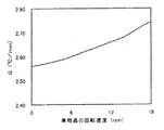
【図2】単結晶の回転速度と結晶温度勾配Gとの関係の一例を示すグラフである。
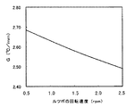
【図3】ルツボの回転速度と結晶温度勾配Gとの関係の一例を示すグラフである。
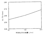
【図4】不活性ガスの流量と結晶温度勾配Gとの関係の一例を示すグラフである。
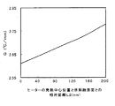
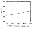
【図5】ヒーターの発熱中心位置から原料融液面までの相対距離L2と結晶温度勾配Gとの関係の一例を示すグラフである。
【図6】チャンバ内の圧力と結晶温度勾配Gとの関係の一例を示すグラフである。
【図7】原料融液に印加する磁場の磁場強度と結晶温度勾配Gとの関係の一例を示すグラフである。
【図8】原料融液面と原料融液に印加する磁場の磁場中心間の相対距離L3と結晶温度勾配Gとの関係の一例を示すグラフである。
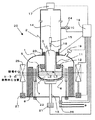
【図9】本発明の単結晶の製造方法を実施する際に使用することのできる単結晶引上げ装置の一例を説明する構成概略図である。
【図10】V/Gと結晶欠陥分布の関係を表す説明図である。
【図11】(a)は、実施例1及び比較例において単結晶を育成するときの単結晶直胴部の成長軸方向の長さと引上げ速度との関係を示したグラフであり、(b)は、単結晶直胴部の成長軸方向の長さと原料融液面と遮熱部材間の距離L1との関係を示したグラフであり、(c)は、実施例1及び比較例で作製したシリコン単結晶の欠陥領域を模式的に示した図である。
【図12】(a)は、実施例2における単結晶直胴部の成長軸方向の長さと引上げ速度との関係を示したグラフであり、(b)は、単結晶直胴部の成長軸方向の長さと単結晶の回転速度との関係を示したグラフである。
【図13】(a)は、実施例3における単結晶直胴部の成長軸方向の長さと引上げ速度との関係を示したグラフであり、(b)は、単結晶直胴部の成長軸方向の長さとアルゴンガスの流量との関係を示したグラフである。
【図14】(a)は、実施例4における単結晶直胴部の成長軸方向の長さと引上げ速度との関係を示したグラフであり、(b)は、単結晶直胴部の成長軸方向の長さとルツボの回転速度との関係を示したグラフである。
【図15】(a)は、実施例5における単結晶直胴部の成長軸方向の長さと引上げ速度との関係を示したグラフであり、(b)は、単結晶直胴部の成長軸方向の長さとチャンバ内の圧力との関係を示したグラフである。
【図16】(a)は、実施例8における単結晶直胴部の成長軸方向の長さと引上げ速度との関係を示したグラフであり、(b)は、単結晶直胴部の成長軸方向の長さと加熱ヒーターの発熱中心位置と原料融液面間の相対距離L2との関係を示したグラフである。
【符号の説明】
1…メインチャンバ、 2…引上げチャンバ、
3…単結晶(シリコン単結晶)、 4…原料融液、 5…石英ルツボ、
6…黒鉛ルツボ、 7…加熱ヒーター、 8…断熱材、
9…ガス流出口、 10…ガス導入口、 11…ガス整流筒、
12…遮熱部材、 13…保持軸、 14…ワイヤー、
15…種ホルダー、 16…種結晶、 17…引上げ機構、
18…引上げ条件制御手段、 19…CCDカメラ、
20…単結晶引上げ装置、 21…ルツボ駆動機構、
22…ヒーター駆動手段、 23…遮熱部材駆動手段、
24,26…バルブ、 25…磁場発生装置、
27…磁場発生装置駆動手段。[0001]
BACKGROUND OF THE INVENTION
The present invention relates to a method for producing a single crystal by the Czochralski method, and more particularly to a method for producing a single crystal having a predetermined crystal diameter and a desired defect region.
[0002]
[Prior art]
As a single crystal used as a substrate of a semiconductor device, for example, there is a silicon single crystal or the like, and it is mainly manufactured by a Czochralski method (hereinafter abbreviated as CZ method). In recent years, high integration has been promoted in semiconductor devices, and miniaturization of elements has progressed. Accordingly, the problem of grown-in defects introduced during single crystal growth has become more important.
[0003]
Here, the grow-in defect will be described with reference to FIG.
In general, when a silicon single crystal is grown, if the crystal growth rate V (crystal pulling rate) is relatively high, FPD (Flow Pattern Defect), which is caused by voids in which hole-type point defects are gathered, is assumed. Grown-in defects such as COP (Crystal Originated Particle) and the like exist in high density throughout the crystal diameter direction. A region where defects due to these voids exist is called a V (vacancy) region.
[0004]
Further, when the crystal growth rate is lowered, an OSF (Oxidation Induced Stacking Fault) region is generated in a ring shape from the periphery of the crystal as the growth rate is lowered, and when the growth rate is further lowered, the OSF is reduced. The ring shrinks to the center of the wafer and disappears. On the other hand, when the growth rate is further reduced, defects such as LSEPD (Large Secco Etch Pit Defect) and LFPD (Large Flow Pattern Defect), which are considered to be caused by dislocation loops in which interstitial silicon has gathered, exist at low density. The region where the defect exists is called an I (Interstitial) region.
[0005]
In recent years, it has been discovered that there is an area outside the OSF ring between the V region and the I region, where there are no defects such as FPD and COP caused by voids and no defects such as LSEPD and LFPD caused by interstitial silicon. This region is called an N (neutral) region. Further, this N region is further classified into an Nv region (region with many vacancies) adjacent to the outside of the OSF ring and a Ni region (region with a lot of interstitial silicon) adjacent to the I region. In the Nv region, It is known that the amount of precipitated oxygen is large when the thermal oxidation treatment is performed, and there is almost no oxygen precipitation in the Ni region.
[0006]
Furthermore, after thermal oxidation treatment, it has been found that there is a region (hereinafter referred to as Cu deposition defect region) in which defects detected by Cu deposition treatment are remarkably generated in a part of the Nv region where oxygen precipitation is likely to occur. This has been found to cause deterioration of electrical characteristics such as oxide film breakdown voltage characteristics.
[0007]
These grow-in defects are caused by a pulling rate V (mm / min) when growing a single crystal and a crystal temperature gradient G (° C / mm) in the pulling axial direction between 1400 ° C and the melting point of silicon near the solid-liquid interface. Ratio V / G (mm2The introduction amount is considered to be determined by a parameter of / ° C./min) (see, for example, Non-Patent Document 1). That is, a single crystal having a desired defect region or a desired defect-free region can be manufactured by growing a single crystal while V / G is controlled to be constant at a predetermined value.
[0008]
For example, in
[0009]
In general, the crystal temperature gradient G in the pulling axis direction is uniquely determined by HZ (hot zone: in-furnace structure) of a single crystal pulling apparatus in which single crystals are grown. However, since it is extremely difficult to change HZ during pulling of the single crystal, when the single crystal is grown by controlling V / G as described above, the crystal temperature gradient G is controlled during pulling of the single crystal. However, a single crystal having a desired defect region is manufactured by controlling the V / G value by adjusting the pulling rate V.
[0010]
Further, in the conventional production of a single crystal, in order to control the diameter of the single crystal to be grown, the temperature of the raw material melt is adjusted by adjusting the pulling rate of the single crystal or changing the power of the heater for heating the raw material melt. It has been done to adjust. However, in the case of growing a single crystal having a desired defect region by controlling the V / G value as described above, the V / G is controlled by adjusting the pulling speed and at the same time the diameter control of the single crystal. However, if the pulling speed is greatly changed in order to make the crystal diameter a desired size at this time, the defect region of the pulled single crystal changes, and the single crystal is There was a problem that it was not possible to grow in the area, resulting in a decrease in yield.
[0011]
Therefore, conventionally, in order to improve such a problem as much as possible, a single crystal can be grown in a desired defect region while suppressing fluctuations in the crystal pulling rate, and a heater is used to control the crystal diameter to a desired value. The temperature of the raw material melt was adjusted by changing the power. However, even if the single crystal is grown in this way, it is very difficult to grow the entire single crystal straight body portion with a predetermined diameter and to have a desired defect region. In order to control the temperature of the raw material melt in order to control the crystal diameter, it is necessary to change the set temperature pattern of the raw material melt for each single crystal pulling device and each single crystal production batch. Therefore, it is necessary to adjust the temperature pattern for each single crystal pulling apparatus or each manufacturing batch, and it takes a lot of labor to manufacture a single crystal in a desired defect region while controlling the diameter. The burden on the work was very heavy.
[0012]
[Patent Document 1]
JP-A-11-147786
[Non-Patent Document 1]
V. V. Voronkov, Journal of Crystal Growth, 59 (1982), 625-643
[0013]
[Problems to be solved by the invention]
Therefore, the present invention has been made in view of the above problems, and an object of the present invention is to stabilize the single crystal diameter control and V / G control when growing the single crystal by the CZ method. It is an object of the present invention to provide a method for producing a single crystal which can be produced easily and can produce a single crystal having a predetermined crystal diameter and a desired defect region easily and with a high yield.
[0014]
[Means for Solving the Problems]
In order to achieve the above object, according to the present invention, in a method for producing a single crystal by pulling it up from a raw material melt in a chamber by the Czochralski method, the single crystal is directly grown when the single crystal is grown. The diameter of the straight body of the single crystal is expressed as V (mm / min) as the pulling speed when growing the body and G (° C./mm) as the crystal temperature gradient in the pulling axis direction near the solid-liquid interface. The single crystal is pulled while controlling / changing the pulling speed V so that becomes a predetermined value, and the crystal temperature gradient G is controlled by changing the pulling condition of the single crystal according to the fluctuation of the pulling speed V. Ratio V / G (mm of pulling speed V and crystal temperature gradient G2/.Degree. C./min) is controlled so that a single crystal having a desired defect region can be grown..
[0015]
Thus, when a single crystal is grown by the CZ method, the crystal diameter can be stably controlled by controlling and changing the pulling rate V, and at the same time, other single crystals can be controlled according to the variation of V. By controlling the crystal temperature gradient G by changing the pulling conditions, the V / G can be stably controlled so that a single crystal having a desired defect region can be grown. Then, by growing the single crystal while performing the diameter control and the V / G control in this manner, the single crystal has a predetermined crystal diameter over the entire straight body of the single crystal, and a desired defect region is formed. A high-quality single crystal can be easily manufactured with a high yield.
[0016]
At this time, the single crystal pulling conditions to be changed when growing the single crystal are the distance between the melt surface of the raw material melt and the heat shield member disposed opposite to the raw material melt surface in the chamber, and the single crystal pulling condition. The rotational speed of the single crystal when pulling up the crystal, the rotational speed of the crucible containing the raw material melt, the flow rate of the inert gas introduced into the chamber, the position of the heater for heating the raw material melt, the inside of the chamber Preferably, at least one of a pressure, a magnetic field strength of a magnetic field applied to the raw material melt, and a relative distance between the raw material melt surface and the magnetic field center of the magnetic field applied to the raw material melt..
[0017]
Thus, when growing a single crystal, the crystal temperature gradient G can be easily controlled in accordance with fluctuations in the pulling rate V by changing at least one of the single crystal pulling conditions shown above. Accordingly, V / G can be stably controlled with high accuracy so that a single crystal having a desired defect region can be grown.
[0018]
In this case, it is preferable to control the V / G so that the defect region of the single crystal to be grown becomes an N region over the entire surface in the radial direction..
In this way, by controlling the V / G so that the defect region of the single crystal becomes the N region in the entire radial direction, defects caused by voids such as FPD and COP in the single crystal straight body portion can also be caused by LSEPD, LFPD. It is possible to produce a very high quality single crystal with a high yield without defects such as dislocation loops and the like, and with a crystal diameter controlled with high accuracy.
[0019]
The diameter of the straight body of the single crystal can be 200 mm or more..
The method for producing a single crystal of the present invention can be very effectively applied to the production of a large-diameter single crystal having a diameter of 200 mm or more, and a single crystal straight body portion that has been difficult to produce conventionally. Thus, a large-diameter single crystal having a diameter of 200 mm or more, which becomes a desired defect region, can be easily and very stably manufactured.
[0020]
Furthermore, the single crystal to be manufactured can be a silicon single crystal..
As described above, the method for producing a single crystal of the present invention can be particularly preferably used for producing a silicon single crystal. By producing a silicon single crystal according to the present invention, the diameter of the silicon single crystal can be increased during the growth of the silicon single crystal. Control and V / G control can be performed stably, and a high-quality silicon single crystal having a predetermined crystal diameter and having a desired defect region over the entire straight body can be easily obtained. And it can manufacture with a high yield.
[0021]
And according to this invention, the single crystal manufactured by the manufacturing method of the said single crystal is provided..
The single crystal produced according to the present invention can be a very high quality single crystal having a predetermined crystal diameter uniformly over the entire area of the single crystal straight body and having a desired defect region.
[0022]
DETAILED DESCRIPTION OF THE INVENTION
Hereinafter, although an embodiment is described about the present invention, the present invention is not limited to these.
The inventors of the present invention have repeatedly studied a method capable of easily and high yielding a single crystal having a predetermined crystal diameter and a desired defect region by the CZ method, and increasing the pulling speed V when pulling up the single crystal. If the diameter can be controlled by controlling and changing, and the crystal temperature gradient G in the pulling axis direction between the melting point of silicon near the solid-liquid interface and 1400 ° C. can be controlled during pulling of the single crystal, For control, it was considered that V / G can be controlled even if the pulling speed V is greatly changed, and a single crystal having a predetermined crystal diameter and a desired defect region can be easily grown with a high yield.
[0023]
Therefore, as a result of further experiments and examinations, the present inventors, as a result, a heat shielding member disposed so as to face the melt surface of the raw material melt and the raw material melt surface when the single crystal is grown by the CZ method, Distance, rotation speed of the single crystal for rotating the single crystal, rotation speed of the crucible containing the raw material melt, flow rate of the inert gas introduced into the chamber, position of the heater for heating the raw material melt, Pay attention to the single crystal pulling conditions such as pressure, magnetic field strength of the magnetic field applied to the raw material melt, and relative distance between the raw material melt surface and the magnetic field center of the magnetic field applied to the raw material melt. It has been found that the crystal temperature gradient G in the pulling axis direction between the melting point of silicon near the solid-liquid interface and 1400 ° C. can be controlled by intentionally changing the single crystal pulling. Pull The V / G was found to be controlled with high accuracy in a desired defect region by also varying the lower speed V to alter or control the crystal temperature gradient G.
[0024]
In addition, the present inventors have developed a comprehensive heat transfer analysis software FEMAG (F. Dupret, P. Nicodeme, Y. Ryckmans, P. Waters, and M. J. Crochet, Int. J. Heat Mass Transfer, 33, 1849 (1990). )), A simulation analysis was performed on the change in the crystal temperature gradient G when the single crystal pulling conditions described above were changed when growing the single crystal. 1 to 8, changes in G when the distance L1 between the raw material melt surface and the heat shield member is changed during pulling of the single crystal, changes in G when the rotation speed of the single crystal is changed, The change in G when the rotational speed of the crucible is changed, the change in G when the flow rate of the inert gas is changed, the position of the heat generation center of the heater and the raw material melt surface when the heater position is changed Change in G relative to the relative distance L2, change in G when the pressure in the chamber is changed, change in G when the magnetic field strength applied to the raw material melt is changed, applied to the raw material melt surface and the raw material melt An example of the result of simulation analysis for each change in G when the relative distance L3 of the magnetic field to be performed is changed is shown.
[0025]
As shown in FIG. 1 to FIG. 8, as a result of simulation analysis, it is clear that the crystal temperature gradient G changes by changing each pulling condition shown above. Decrease the distance L1 between the surface and the heat shield member, increase the rotation speed of the single crystal, decrease the rotation speed of the crucible, increase the flow rate of the inert gas, the heat generation center position of the heater and the raw material melt surface The crystal temperature gradient is obtained by changing the heater position so that the relative distance L2 is increased, decreasing the pressure in the chamber, increasing the magnetic field strength, or decreasing the relative distance L3 between the raw material melt surface and the magnetic field center. G can be increased, and on the other hand, the crystal temperature gradient G can be reduced by changing each single crystal pulling condition with the above increase and decrease reversed. It was bought.
[0026]
Furthermore, when the time (responsiveness) until the crystal temperature gradient G changes when the above single crystal pulling conditions are changed during single crystal pulling is investigated, When the distance L1 between the heat shield members, the rotation speed of the single crystal, and the flow rate of the inert gas are changed, the crystal temperature gradient G also changes immediately according to the change of the pulling conditions, and quick response It was found that the crystal temperature gradient G is very suitable for the fluctuation of the pulling rate V in a relatively short period. In addition, when the crucible rotation speed, the heater position, the pressure in the chamber, the magnetic field strength, and the relative distance L3 between the raw material melt surface and the magnetic field center are changed, the crystal temperature gradient G changes gently. It has been found that it is suitable for controlling the crystal temperature gradient G with respect to the fluctuation of the pulling speed V having a relatively long period. It has been found that if these are controlled in combination, V / G can be controlled within a predetermined value with high accuracy against various fluctuations in the pulling speed V.
[0027]
The present invention utilizes the relationship between the single crystal pulling condition during the pulling of the single crystal and the crystal temperature gradient G as described above to control the single crystal diameter and V / G when growing the single crystal. It can be performed very stably.
That is, according to the method for producing a single crystal of the present invention, when the single crystal is grown by the CZ method, the single crystal is pulled while controlling and changing the pulling speed V so that the diameter of the single crystal straight body portion becomes a predetermined value. In addition, the crystal temperature gradient G is controlled by changing the single crystal pulling conditions according to the fluctuation of the pulling speed V, and V / G is set to a desired value so that a single crystal having a desired defect region can be grown. It is characterized by control.
[0028]
Hereinafter, although the manufacturing method of the single crystal of this invention is demonstrated in detail, referring drawings, this invention is not limited to this.
The single crystal pulling apparatus used in the method for producing a single crystal according to the present invention includes a distance L1 between the raw material melt surface and the heat shield member during the pulling of the single crystal, the rotation speed of the single crystal, the rotation speed of the crucible, and an inert gas. Flow rate, heater position, chamber pressure, magnetic field strength applied to the raw material melt, and relative distance L3 between the raw material melt surface and the magnetic field center applied to the raw material melt. Although it will not specifically limit if crystal pulling conditions can be changed, For example, a single crystal pulling apparatus as shown in FIG. 9 can be used. First, a single crystal pulling apparatus that can be used when carrying out the method for producing a single crystal of the present invention will be described with reference to FIG.
[0029]
In the single
[0030]
A pulling
[0031]
Further, a
[0032]
An inert gas such as argon gas can be introduced from the
[0033]
Further, a
[0034]
The pulling
[0035]
The single crystal pulling apparatus that can be used in the present invention is not limited to the above-described apparatus, and a cooling jacket for cooling the
[0036]
In the case of growing, for example, a silicon single crystal by the CZ method using such a single
[0037]
In the present invention, when the straight body portion of the silicon
[0038]
More specifically, for example, when a silicon single crystal is grown so that the defect region is an N region over the entire surface in the radial direction, after the seed restriction is formed as described above, the diameter is expanded until the diameter reaches a predetermined value. After the diameter, the pulling speed V is adjusted according to the manufacturing environment (for example, HZ of the single crystal pulling apparatus) in which the single crystal is manufactured so that the straight body portion of the single crystal can be grown in the N region.
[0039]
Then, when growing the diameter of the single crystal straight body portion, the pulling speed V is controlled and changed so that the diameter of the single crystal straight body portion is maintained at a predetermined value, and according to the fluctuation of the pulling speed V. The distance L1 between the raw material melt surface and the heat shield member, the rotation speed of the single crystal, the rotation speed of the crucible, the flow rate of the inert gas introduced into the chamber, the position of the heater, the pressure in the chamber, the magnetic field strength, the raw material melting The crystal temperature gradient G is controlled by changing at least one single crystal pulling condition of the relative distance L3 between the liquid level and the magnetic field center. At this time, other factors that can change the crystal temperature gradient G may be simultaneously controlled and changed.
[0040]
For example, when the pulling speed is increased in order to maintain the diameter of the straight body portion at a predetermined value, in order to increase the crystal temperature gradient G according to the increase of the pulling speed V, between the raw material melt surface and the heat shield member The distance L1 is decreased, the rotation speed of the single crystal is increased by the pulling
[0041]
Note that the distance L1 between the raw material melt surface and the heat shield member is set so that the quartz crucible 5 and the
[0042]
On the other hand, in the case where the pulling speed is slowed down in order to control the diameter of the straight body portion, the distance between the raw material melt surface and the heat shield member is reduced in order to reduce the crystal temperature gradient G according to the decrease in the pulling speed V. Increase L1, decrease single crystal rotation speed, increase crucible rotation speed, decrease flow rate of inert gas, decrease relative distance L2 between the center of heat generation of the heater and the raw material melt surface Of the single crystal pulling conditions such as raising the position of the heater 7, increasing the pressure in the chamber, decreasing the magnetic field strength, and increasing the relative distance L3 between the raw material melt surface and the magnetic field center Do at least one of the following:
[0043]
As described above, among the single crystal pulling conditions shown above, the distance L1 between the raw material melt surface and the heat shield member, the rotation speed of the single crystal, and the flow rate of the inert gas were changed. Sometimes the crystal temperature gradient G also changes quickly and shows a quick response. Also, the crucible rotation speed, the position of the heater, the pressure in the chamber, the magnetic field strength, the relative distance L3 between the raw material melt surface and the magnetic field center. Gradually changes the crystal temperature gradient G. Further, regarding the magnetic field strength and the relative distance L3 between the raw material melt surface and the magnetic field center, for example, the magnetic field strength is adjusted by the
[0044]
Therefore, in consideration of the characteristics of each single crystal pulling condition as described above, for example, the distance L1 between the raw material melt surface having excellent G response and the heat shielding member, the rotation speed of the single crystal, the flow rate of the inert gas Is preferably changed with respect to the fluctuation of the pulling speed V in a relatively short cycle. Based on this, by changing the distance L1 between the raw material melt surface and the heat shield member, the single crystal rotation speed, and the flow rate of the inert gas, the V / G can be controlled with high accuracy.
[0045]
Further, the rotational speed of the crucible for gradually changing G, the position of the heater, and the pressure in the chamber are preferably changed in response to fluctuations in the pulling speed from a short cycle to a long cycle, for example, several minutes to several tens of minutes The crystal temperature gradient G may be controlled by changing the pulling conditions based on the fluctuations in the average value of the pulling rates obtained over a relatively long period of time. Further, if the magnetic field strength and the relative distance L3 between the raw material melt surface and the magnetic field center are changed, the change in G is gentle and the magnetic field strength and the magnetic field center actually applied to the raw material melt change. Since it takes time to do so, an average value of the pulling speed is obtained in a very long time, for example, 5 minutes or more, and based on the fluctuation of the average value of the pulling speed, that is, the fluctuation of the pulling speed V in a long cycle. It is preferable to change the magnetic field strength and the relative distance L3 between the raw material melt surface and the magnetic field center. By calculating the average value of the pulling speed at different time intervals depending on the single crystal pulling condition thus changed, and changing each single crystal pulling condition based on the fluctuation of the average value of the pulling speed thus determined, It becomes possible to control the crystal temperature gradient G with high accuracy in accordance with fluctuations in the pulling speed, thereby controlling the V / G with very high accuracy and stably growing a single crystal in a desired defect region. be able to.
[0046]
Furthermore, in the present invention, when growing a single crystal, the crystal temperature gradient G is controlled by changing two or more of the single crystal pulling conditions shown above according to the fluctuation of the pulling speed V. Can also be done. Normally, each of the above single crystal pulling conditions also affects various other manufacturing conditions such as crystal quality when growing a single crystal. Therefore, depending on the manufacturing environment of the single crystal, there may be a concern that various inconveniences may occur if only one pulling condition is changed greatly. For example, if the distance L1 between the raw material melt surface and the heat shield member is excessively widened, or if the flow rate of the inert gas is excessively increased, the operability during single crystal growth may be deteriorated. If the rotational speed of the crucible and the rotational speed of the crucible become too fast or too slow, the shape of the single crystal straight body will be deformed, the quality distribution in the crystal plane will be deteriorated and the yield will be reduced. It is possible that inconvenience may occur.
[0047]
However, when growing a single crystal as described above, the crystal temperature gradient G can be increased over a wider range than when one pulling condition is changed by changing two or more of the single crystal pulling conditions. In addition, the control accuracy and responsiveness of the crystal temperature gradient G can be improved by changing the pulling conditions. Further, for example, when the crystal temperature gradient G is increased, the distance L1 between the raw material melt surface and the heat shielding member is reduced, while when the crystal temperature gradient G is decreased, the flow rate of the inert gas is decreased. By doing so, it becomes possible to control the crystal temperature gradient G without deteriorating the operability and reducing the influence on various other manufacturing conditions. Furthermore, for example, the single crystal pulling condition to be changed with respect to the fluctuation of the pulling speed with a relatively short cycle such as the distance L1 between the raw material melt surface and the heat shield member, If the single crystal pulling condition is changed in combination with the single crystal pulling condition that is changed with respect to the long-period pulling speed fluctuation, the crystal temperature gradient G can be controlled with higher accuracy with respect to various pulling speed V fluctuations. Thus, a single crystal having a desired defect region can be manufactured very stably.
[0048]
In the present invention, the distance L1 between the raw material melt surface and the heat shield member during single crystal growth, the rotation speed of the single crystal, the rotation speed of the crucible, the flow rate of the inert gas, the position of the heater, the pressure in the chamber It is sufficient to change at least one of the magnetic field strength, the relative distance L3 between the raw material melt surface and the magnetic field center, and depending on the manufacturing environment (for example, the structure of HZ) where the single crystal is actually manufactured, etc. The number and parameters of pulling conditions to be changed can be selected as appropriate. It is also possible to control and change factors other than the above simultaneously.
[0049]
Further, the control range of each pulling condition when changing the pulling condition can be appropriately determined according to the production environment of the single crystal and is not particularly limited. If one pulling condition is changed too much, there is a risk that the above-mentioned disadvantages occur. Therefore, during the single crystal pulling, it is preferable to change each single crystal pulling condition within a range in which the single crystal can be stably grown.
[0050]
For example, when changing the distance L1 between the raw material melt surface and the heat shield member during single crystal growth, depending on the diameter of the single crystal to be pulled up, the distance L1 is 1 to 500 mm, preferably 10 to 300 mm, Preferably, it is desirable to change in the range of 20 to 200 mm. Similarly, in the case of the rotational speed of the single crystal, it is changed in the range of 0.1 to 40 rpm, preferably 5 to 20 rpm, and in the case of the rotational speed of the crucible. Change in the range of 0.1 to 40 rpm, change in the range of 10 to 2000 L / min, preferably in the range of 60 to 300 L / min for the flow rate of the inert gas, and the position of the heater is the center of heat generation of the heater Heater position so that the relative distance L2 between the surface and the raw material melt surface varies in the range of 0 to 500 mm, preferably 10 to 200 mm, more preferably 30 to 100 mm. The pressure in the chamber is changed in the range of 5 to 300 mbar, preferably 10 to 200 mbar, the magnetic field strength is changed in the range of 100 to 10000 G, preferably 500 to 6000 G, and the raw material melt surface and the magnetic field are changed. In the case of the relative distance L3 from the center, it is desirable to change within a range of 0 to 1000 mm, preferably 5 to 500 mm.
[0051]
Furthermore, in the present invention, by using the pulling condition control means 18 shown in FIG. 9, the pulling speed V is automatically controlled and changed so that the diameter of the single crystal becomes a predetermined value during pulling of the single crystal. The crystal temperature gradient G can be automatically controlled according to the fluctuation of the pulling speed V. Specifically, for example, during the pulling of the single crystal, the position of the raw material melt surface measured by the
[0052]
As described above, according to the present invention, during the pulling of the single crystal, the pulling speed V is controlled and changed so that the diameter of the single crystal straight body portion becomes a predetermined value, and the raw material melt is changed according to the fluctuation of the pulling speed V. The distance L1 between the liquid surface and the heat shield member, the rotation speed of the single crystal, the rotation speed of the crucible, the flow rate of the inert gas introduced into the chamber, the position of the heater, the pressure in the chamber, the magnetic field strength, and the raw material melt surface By changing at least one of the relative distances L3 from the magnetic field center and controlling the crystal temperature gradient G, V / G can be stably controlled so that a single crystal having a desired defect region can be grown. Can do. Therefore, the single crystal diameter control and V / G control can be stably performed during the single crystal pulling without performing the temperature pattern adjustment for each single crystal pulling apparatus or each manufacturing batch as in the prior art. For example, even a large-diameter single crystal having a diameter of 200 mm or more has a predetermined crystal diameter over the entire straight body portion of the single crystal and has a very high defect area. Quality single crystals can be manufactured much more easily and with a higher yield.
[0053]
Furthermore, when the single crystal is grown, the controllability of V / G can be improved by controlling the crystal temperature gradient G according to the fluctuation of the pulling rate V as in the present invention. Therefore, for example, as shown in FIG. 10, it is possible to manufacture a single crystal by controlling V / G with high precision in a narrow region such as an Nv region or an Ni region in an N region that does not include a Cu deposit defect region, A high-quality single crystal having a desired defect region can be obtained very stably.
[0054]
In the present invention, it is also possible to install a cooling jacket for cooling the
[0055]
【Example】
EXAMPLES Hereinafter, although an Example and a comparative example are shown and this invention is demonstrated more concretely, this invention is not limited to these.
(Example 1: Change of the distance L1 between a raw material melt surface and a heat shield member)
Using a single
[0056]
While the straight body portion of the silicon single crystal is grown, the diameter of the single crystal body portion is measured by the
[0057]
FIGS. 11A and 11B show the pulling rate V and the rate of change in the distance L1 between the raw material melt surface and the heat shield member, respectively, changed during the single crystal growth. As shown in FIG. 11 (a), the reason why the pulling speed is high within a range of 10 cm or less in the straight body portion is that the shoulder portion is pulled up from the enlarged diameter portion to enter the straight body portion. By forming the shoulder portion, it is possible to shift to pulling up the straight body portion and to stably control the diameter of the straight body portion.
[0058]
Next, after cutting out the wafer for inspection from each part in the growth axis direction of the single crystal grown as described above, surface grinding and polishing are performed to prepare a sample for inspection, and the crystal as shown below Quality characteristics were inspected.
[0059]
(1) Inspection of FPD (V region) and LSEPD (I region)
After inspecting the sample for inspection for 30 minutes without stirring, the inside of the wafer surface was observed with a microscope to confirm the presence or absence of crystal defects.
(2) Inspection of OSF
The sample for inspection was heat-treated at 1100 ° C. for 100 minutes in a wet oxygen atmosphere, and then the presence of OSF was confirmed by observing the wafer surface with a microscope.
(3) Inspection of defects by Cu deposition process
After forming an oxide film on the surface of the sample for inspection, Cu deposition treatment was performed to confirm the presence or absence of oxide film defects. The evaluation conditions at that time are as follows.
Oxide film: 25nm
Electrolytic strength: 6MV / cm
Voltage application time: 5 minutes
[0060]
(Comparative example)
150 kg of raw material polycrystalline silicon is charged into a quartz crucible having a diameter of 24 inches (600 mm) using the same single
[0061]
Further, while the straight body portion of the silicon single crystal is grown, the diameter of the single crystal straight body portion is measured by the
[0062]
The rate of change in pulling speed V in this comparative example is shown in FIG. 11 (a) (substantially the same value as pulling speed V in Example 1). FIG. 11B shows the value of the distance L1 between the raw material melt surface during the body growth and the heat shield member (constant during single crystal growth).
And after cutting out the wafer for inspection from each part of the growth axis direction of the single crystal obtained above, surface grinding and polishing are performed to produce a sample for inspection, and the same crystal quality characteristics as in Example 1 Inspection was conducted.
[0063]
As a result of examining the crystal quality characteristics of each of the silicon single crystals produced in Example 1 and the comparative example as described above, the silicon single crystal produced in Example 1 was changed from a single crystal
[0064]
On the other hand, in the silicon single crystal produced in the comparative example, OSF is observed in the region of 40 to 55 cm of the straight body portion where the pulling speed V greatly fluctuates, and in the region of 65 to 75 cm of the straight body portion, LSEPD (I Area) was observed. Here, in order to make it easy to compare the results of the inspection of the crystal quality characteristics of the silicon single crystals produced in Example 1 and the comparative example, a diagram schematically showing the defect region of each single crystal is shown in FIG. Shown in (c).
[0065]
(Example 2: Change of rotation speed of single crystal, Example 3: Change of flow rate of inert gas)
Using the single
[0066]
In addition, while the straight body portion of the silicon single crystal is grown, in Example 2, the pulling speed V is controlled and changed so that the diameter of the straight body portion of the silicon single crystal becomes 200 mm as in Example 1 above. In order to change the rotation speed of the single crystal according to the fluctuation of the pulling speed V, the average value of the pulling speeds for 2 minutes is obtained, and the average value of the pulling speeds is increased by 0.02 mm / min. Is a rate at which the rotation speed of the single crystal is increased by 3.0 rpm, and when the average value of the pulling rate is decreased by 0.02 mm / min, the rotation speed of the single crystal is increased by a rate of 3.0 rpm. The pulling
[0067]
Further, in Example 3, the pulling speed V is controlled and changed so that the diameter of the straight body of the silicon single crystal is 200 mm, and the flow rate of the inert gas (argon gas) according to the fluctuation of the pulling speed V. Therefore, when the average value of the pulling rate for 2 minutes is increased by 0.02 mm / min, the flow rate of argon gas is increased by 50 L / min, and the average value of the pulling rate is 0.02 mm. The
[0068]
Here, the rate of change in pulling speed V and single crystal rotation speed changed during single crystal growth as described above in Example 2 is shown in FIGS. 12 (a) and 12 (b), respectively. The rate of change in pulling speed V and the flow rate of argon gas changed during single crystal growth in Example 3 are shown in FIGS. 13 (a) and 13 (b), respectively.
[0069]
And after cutting out the wafer for inspection from each part of the growth axis direction of the single crystal obtained in each of the above Example 2 and Example 3, surface grinding and polishing are performed to produce a sample for inspection, The same crystal quality characteristics were tested as in Example 1. As a result, both the silicon single crystals produced in Example 2 and Example 3 are N regions in which no Cu deposition defects are detected in all regions except the range of the straight body portion of the single crystal straight body portion within 10 cm. It was confirmed that
[0070]
(Example 4: Change of crucible rotation speed, Example 5: Change of pressure in the chamber)
Using the single
[0071]
Further, while the straight body portion of the silicon single crystal is grown, in Example 4, the pulling speed V is controlled and changed so that the diameter of the straight body portion of the silicon single crystal becomes 200 mm as in Example 1 above. In order to change the rotation speed of the crucible according to the fluctuation of the pulling speed V, the average value of the pulling speed for 10 minutes is obtained, and when the average value of the pulling speed is increased by 0.01 mm / min Pulling condition control means at such a rate that the rotational speed of the crucible is reduced by 0.5 rpm, and when the average value of the pulling speed is reduced by 0.01 mm / min, the rotational speed of the crucible is increased by 0.5 rpm. 18, the
[0072]
Furthermore, in Example 5, the pulling speed V is controlled and changed so that the diameter of the straight body of the silicon single crystal is 200 mm, and the pressure in the chamber is changed according to the fluctuation of the pulling speed V. When the average pulling speed for 10 minutes is increased by 0.01 mm / min, the pressure in the chamber is reduced by 25 mbar, and when the average pulling speed is decreased by 0.01 mm / min. The
[0073]
Here, the rate of change in pulling speed V and crucible rotation speed changed during single crystal growth in Example 4 is shown in FIGS. 14A and 14B, respectively. FIG. 15A and FIG. 15B show the pulling speed V and the rate of change in the pressure in the chamber, respectively, changed during single crystal growth in FIG.
[0074]
And after cutting out the wafer for inspection from each part of the growth axis direction of the single crystal obtained in each of Example 4 and Example 5 above, surface grinding and polishing are performed to produce a sample for inspection, The same crystal quality characteristics were tested as in Example 1. As a result, in both the silicon single crystals produced in Example 4 and Example 5, although crystal defects were observed in some very small crystal parts, the range of the straight body portion of the single crystal straight body portion within 10 cm. It was found that the N region in which no Cu deposition defect was detected was in the region of 95% or more excluding. Therefore, in the silicon single crystals of Example 4 and Example 5, the set temperature pattern of the raw material melt is changed for each of the above comparative examples and for each single crystal pulling apparatus or single crystal production batch. Even when compared with a method of producing a single crystal with a predetermined crystal diameter, it was confirmed that a yield equal to or higher than that could be secured.
[0075]
Incidentally, the reason why crystal defects were observed in a part of the silicon single crystals of Example 4 and Example 5 was that even if the rotational speed of the crucible or the pressure in the chamber was changed according to the fluctuation of the pulling speed, it was actually This is probably because some time lag occurred before the crystal temperature gradient G changed.
[0076]
(Example 6: Change in the distance L1 between the raw material melt surface and the heat shielding member and the flow rate of the inert gas) Using the single
[0077]
Further, while the straight body portion of the silicon single crystal is grown, the pulling speed V is controlled and changed so that the diameter of the straight body portion of the silicon single crystal becomes 200 mm as in the first embodiment. The average value of the pulling speed per minute is obtained, and when the average value of the pulling speed is increased by 0.02 mm / min, the pulling condition is such that the distance L1 between the raw material melt surface and the heat shield member is reduced by 5 mm. When the
[0078]
Then, after inspecting a wafer for inspection from each part in the growth axis direction of the obtained single crystal, surface grinding and polishing are performed to produce a sample for inspection, and the inspection of crystal quality characteristics similar to that in Example 1 is performed. Went. As a result, it was confirmed that the silicon single crystal produced in Example 6 was an N region in which no Cu deposition defect was detected in all regions except the range of the straight body portion within 10 cm of the single crystal straight body portion. did it.
[0079]
(Example 7)
The single
[0080]
In addition, when a plurality of batches of silicon single crystals are continuously produced, when the single crystal straight body portion is grown in each production batch, the pulling speed V is set so that the diameter of the single crystals becomes 200 mm as in the case of Example 6. In addition, the distance L1 between the raw material melt surface and the heat shield member and the flow rate of the inert gas were changed according to the fluctuation of the pulling speed.
[0081]
Then, as a result of performing the inspection of the crystal quality characteristics similar to Example 1 on each single crystal for the plurality of single crystals obtained continuously, all the silicon single crystals are 10 cm in the straight body portion of the single crystal straight body portion. It was confirmed that in all the regions except for the inner range, the N region in which no Cu deposition defect was detected.
[0082]
(Example 8: Change of heater position)
Using the single
[0083]
Further, while the straight body portion of the silicon single crystal is being grown, in Example 8, the pulling speed V is controlled and changed so that the diameter of the straight body portion of the silicon single crystal becomes 200 mm as in Example 1 above. In order to change the position of the heater according to the fluctuation of the pulling speed V, the average value of the pulling speed for 10 minutes is obtained, and when the average value of the pulling speed is increased by 0.01 mm / min When the relative distance L2 between the heat generation center position of the heater and the raw material melt surface is increased by 15 mm, and when the average pulling rate is reduced by 0.01 mm / min, the heat generation center position of the heater and the raw material The heater driving means 22 was adjusted by the pulling condition control means 18 at a rate such that the relative distance L2 to the melt surface was reduced by 15 mm to change the position of the heater.
[0084]
Here, the pulling rate V changed during the single crystal growth as described above in Example 8 and the rate of change in the relative distance L2 between the heating center position of the heater and the raw material melt surface are shown in FIG. Shown in a) and (b).
[0085]
And after cutting out the wafer for an inspection from each site | part of the growth axis direction of the single crystal obtained in the said Example 8, surface grinding and grinding | polishing are performed and the sample for an inspection is produced, It is the same as that of Example 1. Crystal quality characteristics were inspected. As a result, the silicon single crystal produced in Example 8 had a crystal defect of 95% or more excluding the range of the straight body portion of the single crystal straight body portion within 10 cm, although crystal defects were observed in some extremely small crystal parts. It was found that the region was an N region where no Cu deposition defect was detected. Therefore, the silicon single crystal of Example 8 has a predetermined crystal diameter by changing the set temperature pattern of the raw material melt for each of the above comparative examples and the conventional single crystal pulling apparatus and each single crystal production batch. In comparison with the method for producing a single crystal, it was confirmed that a yield equal to or higher than that could be secured.
[0086]
The reason why crystal defects were observed in a part of the silicon single crystal of Example 8 was that the crystal temperature gradient G actually changed even if the position of the heater was changed according to the fluctuation of the pulling speed. This is thought to be due to some time lag.
[0087]
In addition, this invention is not limited to the said embodiment. The above-described embodiment is an exemplification, and the present invention has substantially the same configuration as the technical idea described in the claims of the present invention, and any device that exhibits the same function and effect is the present invention. It is included in the technical scope of the invention.
[0088]
For example, in the above embodiment, the case where a single crystal is grown in an N region is described as an example. However, the present invention is not limited to this, and a desired defect such as a V region, an I region, or an OSF region. Single crystals can also be grown in the region. Further, the present invention can be suitably used in the case of manufacturing a silicon single crystal, but is not limited to this, and can be similarly applied to the case of manufacturing a compound semiconductor single crystal or the like. Further, the present invention is similarly applied to a case where a single crystal is grown without applying a magnetic field to the raw material melt, or a case where a single crystal is grown while applying a magnetic field and a current to the raw material melt (EMCZ method). it can.
[0089]
In addition, the manufacturing method of the single crystal of the present invention is not necessarily limited to the case of carrying out with the entire length of the single crystal straight body, and the diameter is controlled at the pulling speed V over a part of the length, and the pulling speed V This includes the case where the crystal temperature gradient G is controlled in accordance with the fluctuation of the desired defect region. In particular, as described above, the region of 10 cm from the shoulder, which is the first half of the straight body, may not be stable in crystal quality. Therefore, it is preferable to carry out after 5 cm or 10 cm after the straight body, which tends to be in a steady state. .
[0090]
【The invention's effect】
As described above, according to the present invention, when a single crystal is grown, the crystal diameter can be stably controlled by controlling / changing the pulling speed V, and at the same time, the fluctuation of the pulling speed V is varied. By changing the single crystal pulling conditions according to the above and controlling the crystal temperature gradient G, V / G can be stably controlled so that a single crystal having a desired defect region can be grown. Then, by growing the single crystal while performing the diameter control and the V / G control in this manner, the single crystal has a predetermined crystal diameter over the entire straight body of the single crystal, and a desired defect region is formed. A high-quality single crystal can be easily manufactured with a high yield.
[Brief description of the drawings]
FIG. 1 is a graph showing an example of a relationship between a distance L1 between a raw material melt surface and a heat shield member and a crystal temperature gradient G;
FIG. 2 is a graph showing an example of the relationship between the rotation speed of a single crystal and the crystal temperature gradient G.
FIG. 3 is a graph showing an example of the relationship between the rotational speed of the crucible and the crystal temperature gradient G;
4 is a graph showing an example of a relationship between an inert gas flow rate and a crystal temperature gradient G. FIG.
FIG. 5 is a graph showing an example of the relationship between the relative distance L2 from the heating center position of the heater to the raw material melt surface and the crystal temperature gradient G;
6 is a graph showing an example of the relationship between the pressure in the chamber and the crystal temperature gradient G. FIG.
7 is a graph showing an example of the relationship between the magnetic field strength of the magnetic field applied to the raw material melt and the crystal temperature gradient G. FIG.
FIG. 8 is a graph showing an example of the relationship between the crystal temperature gradient G and the relative distance L3 between the raw material melt surface and the magnetic field center of the magnetic field applied to the raw material melt.
FIG. 9 is a schematic configuration diagram illustrating an example of a single crystal pulling apparatus that can be used in carrying out the method for producing a single crystal of the present invention.
FIG. 10 is an explanatory diagram showing the relationship between V / G and crystal defect distribution.
FIG. 11 (a) is a graph showing the relationship between the length in the growth axis direction of a single crystal straight body portion and the pulling speed when growing a single crystal in Example 1 and Comparative Example; These are the graphs which showed the relationship of the length of the growth axis direction of a single-crystal straight body part, and the distance L1 between a raw material melt surface and a thermal-insulation member, (c) produced in Example 1 and the comparative example. It is the figure which showed typically the defect area | region of the silicon single crystal.
12A is a graph showing the relationship between the length in the growth axis direction of the single crystal straight body portion in Example 2 and the pulling rate, and FIG. 12B is the growth axis of the single crystal straight body portion. It is the graph which showed the relationship between the length of a direction, and the rotational speed of a single crystal.
FIG. 13A is a graph showing the relationship between the length in the growth axis direction of the single crystal straight body part and the pulling rate in Example 3, and FIG. 13B is the growth axis of the single crystal straight body part. It is the graph which showed the relationship between the length of a direction, and the flow volume of argon gas.
14 (a) is a graph showing the relationship between the length in the growth axis direction of the single crystal straight body portion and the pulling rate in Example 4, and FIG. 14 (b) is the growth axis of the single crystal straight body portion. It is the graph which showed the relationship between the length of a direction, and the rotational speed of a crucible.
15 (a) is a graph showing the relationship between the length in the growth axis direction of the single crystal straight body portion and the pulling rate in Example 5, and FIG. 15 (b) is the growth axis of the single crystal straight body portion. It is the graph which showed the relationship between the length of a direction, and the pressure in a chamber.
16 (a) is a graph showing the relationship between the length in the growth axis direction of the single crystal straight body part and the pulling rate in Example 8, and FIG. 16 (b) is the growth axis of the single crystal straight body part. It is the graph which showed the relationship between the length of a direction, the heat generation center position of a heater, and the relative distance L2 between raw material melt surfaces.
[Explanation of symbols]
1 ... main chamber, 2 ... pulling chamber,
3 ... single crystal (silicon single crystal), 4 ... raw material melt, 5 ... quartz crucible,
6 ... Graphite crucible, 7 ... Heater, 8 ... Insulating material,
9 ... Gas outlet, 10 ... Gas inlet, 11 ... Gas rectifier,
12 ... Heat shield member, 13 ... Holding shaft, 14 ... Wire,
15 ... Seed holder, 16 ... Seed crystal, 17 ... Pulling mechanism,
18 ... Pulling condition control means, 19 ... CCD camera,
20 ... Single crystal pulling device, 21 ... Crucible drive mechanism,
22 ... heater driving means, 23 ... heat shield member driving means,
24, 26 ... valve, 25 ... magnetic field generator,
27: Magnetic field generator driving means.
Claims (4)
Priority Applications (1)
| Application Number | Priority Date | Filing Date | Title |
|---|---|---|---|
| JP2003185979A JP4457584B2 (en) | 2003-06-27 | 2003-06-27 | Method for producing single crystal and single crystal |
Applications Claiming Priority (1)
| Application Number | Priority Date | Filing Date | Title |
|---|---|---|---|
| JP2003185979A JP4457584B2 (en) | 2003-06-27 | 2003-06-27 | Method for producing single crystal and single crystal |
Publications (2)
| Publication Number | Publication Date |
|---|---|
| JP2005015314A JP2005015314A (en) | 2005-01-20 |
| JP4457584B2 true JP4457584B2 (en) | 2010-04-28 |
Family
ID=34185226
Family Applications (1)
| Application Number | Title | Priority Date | Filing Date |
|---|---|---|---|
| JP2003185979A Expired - Fee Related JP4457584B2 (en) | 2003-06-27 | 2003-06-27 | Method for producing single crystal and single crystal |
Country Status (1)
| Country | Link |
|---|---|
| JP (1) | JP4457584B2 (en) |
Families Citing this family (10)
| Publication number | Priority date | Publication date | Assignee | Title |
|---|---|---|---|---|
| US8147611B2 (en) * | 2005-07-13 | 2012-04-03 | Shin-Etsu Handotai Co., Ltd. | Method of manufacturing single crystal |
| US7427325B2 (en) * | 2005-12-30 | 2008-09-23 | Siltron, Inc. | Method for producing high quality silicon single crystal ingot and silicon single crystal wafer made thereby |
| JP4702266B2 (en) * | 2006-11-10 | 2011-06-15 | 信越半導体株式会社 | Single crystal pulling method |
| JP5136252B2 (en) * | 2008-07-11 | 2013-02-06 | 株式会社Sumco | Method for growing silicon single crystal |
| US8221545B2 (en) * | 2008-07-31 | 2012-07-17 | Sumco Phoenix Corporation | Procedure for in-situ determination of thermal gradients at the crystal growth front |
| JP5145176B2 (en) * | 2008-09-11 | 2013-02-13 | コバレントマテリアル株式会社 | Silicon single crystal pulling apparatus and silicon single crystal pulling method |
| KR101729515B1 (en) | 2015-04-14 | 2017-04-24 | 주식회사 엘지실트론 | Method for growing silicon single crystal ingot |
| DE102019101991A1 (en) * | 2019-01-28 | 2020-07-30 | Pva Tepla Ag | Method of pulling a cylindrical crystal from a melt |
| US11618971B2 (en) * | 2020-09-29 | 2023-04-04 | Sumco Corporation | Method and apparatus for manufacturing defect-free monocrystalline silicon crystal |
| CN115404541B (en) * | 2022-10-18 | 2023-08-25 | 四川晶科能源有限公司 | Crystal pulling method |
-
2003
- 2003-06-27 JP JP2003185979A patent/JP4457584B2/en not_active Expired - Fee Related
Also Published As
| Publication number | Publication date |
|---|---|
| JP2005015314A (en) | 2005-01-20 |
Similar Documents
| Publication | Publication Date | Title |
|---|---|---|
| US7384477B2 (en) | Method for producing a single crystal and a single crystal | |
| JP4193610B2 (en) | Single crystal manufacturing method | |
| JP4457584B2 (en) | Method for producing single crystal and single crystal | |
| US7323048B2 (en) | Method for producing a single crystal and a single crystal | |
| JP4151474B2 (en) | Method for producing single crystal and single crystal | |
| US7214268B2 (en) | Method of producing P-doped silicon single crystal and P-doped N-type silicon single crystal wafer | |
| JP4496723B2 (en) | Single crystal manufacturing method and single crystal manufacturing apparatus | |
| EP1679392A1 (en) | Process for producing single crystal | |
| JP4461776B2 (en) | Method for producing silicon single crystal | |
| JP2005015290A (en) | Method for manufacturing single crystal, and single crystal | |
| JP4345597B2 (en) | Single crystal manufacturing apparatus and single crystal manufacturing method | |
| JP5223513B2 (en) | Single crystal manufacturing method | |
| JP4134800B2 (en) | Graphite heater for single crystal production, single crystal production apparatus and single crystal production method | |
| JP4218460B2 (en) | Graphite heater for single crystal production, single crystal production apparatus and single crystal production method | |
| JP4407192B2 (en) | Single crystal manufacturing method | |
| US20240003047A1 (en) | Method and apparatus for growing silicon single crystal ingots | |
| JP4148060B2 (en) | Graphite heater for single crystal production, single crystal production apparatus and single crystal production method | |
| JP4148059B2 (en) | Graphite heater for single crystal production, single crystal production apparatus and single crystal production method | |
| JP4881539B2 (en) | Method for producing single crystal and single crystal | |
| JP2005015298A (en) | Method for manufacturing single crystal, and single crystal | |
| JP2005015297A (en) | Method for manufacturing single crystal, and single crystal | |
| JP2005015288A (en) | Method for manufacturing single crystal, and single crystal |
Legal Events
| Date | Code | Title | Description |
|---|---|---|---|
| A621 | Written request for application examination |
Free format text: JAPANESE INTERMEDIATE CODE: A621 Effective date: 20060315 |
|
| A977 | Report on retrieval |
Free format text: JAPANESE INTERMEDIATE CODE: A971007 Effective date: 20080829 |
|
| A131 | Notification of reasons for refusal |
Free format text: JAPANESE INTERMEDIATE CODE: A131 Effective date: 20080902 |
|
| A131 | Notification of reasons for refusal |
Free format text: JAPANESE INTERMEDIATE CODE: A131 Effective date: 20091020 |
|
| A521 | Request for written amendment filed |
Free format text: JAPANESE INTERMEDIATE CODE: A523 Effective date: 20091119 |
|
| TRDD | Decision of grant or rejection written | ||
| A01 | Written decision to grant a patent or to grant a registration (utility model) |
Free format text: JAPANESE INTERMEDIATE CODE: A01 Effective date: 20100119 |
|
| A01 | Written decision to grant a patent or to grant a registration (utility model) |
Free format text: JAPANESE INTERMEDIATE CODE: A01 |
|
| A61 | First payment of annual fees (during grant procedure) |
Free format text: JAPANESE INTERMEDIATE CODE: A61 Effective date: 20100201 |
|
| R150 | Certificate of patent or registration of utility model |
Free format text: JAPANESE INTERMEDIATE CODE: R150 Ref document number: 4457584 Country of ref document: JP Free format text: JAPANESE INTERMEDIATE CODE: R150 |
|
| FPAY | Renewal fee payment (event date is renewal date of database) |
Free format text: PAYMENT UNTIL: 20130219 Year of fee payment: 3 |
|
| FPAY | Renewal fee payment (event date is renewal date of database) |
Free format text: PAYMENT UNTIL: 20140219 Year of fee payment: 4 |
|
| R250 | Receipt of annual fees |
Free format text: JAPANESE INTERMEDIATE CODE: R250 |
|
| R250 | Receipt of annual fees |
Free format text: JAPANESE INTERMEDIATE CODE: R250 |
|
| R250 | Receipt of annual fees |
Free format text: JAPANESE INTERMEDIATE CODE: R250 |
|
| S531 | Written request for registration of change of domicile |
Free format text: JAPANESE INTERMEDIATE CODE: R313531 |
|
| R350 | Written notification of registration of transfer |
Free format text: JAPANESE INTERMEDIATE CODE: R350 |
|
| R250 | Receipt of annual fees |
Free format text: JAPANESE INTERMEDIATE CODE: R250 |
|
| R250 | Receipt of annual fees |
Free format text: JAPANESE INTERMEDIATE CODE: R250 |
|
| R250 | Receipt of annual fees |
Free format text: JAPANESE INTERMEDIATE CODE: R250 |
|
| R250 | Receipt of annual fees |
Free format text: JAPANESE INTERMEDIATE CODE: R250 |
|
| R250 | Receipt of annual fees |
Free format text: JAPANESE INTERMEDIATE CODE: R250 |
|
| R250 | Receipt of annual fees |
Free format text: JAPANESE INTERMEDIATE CODE: R250 |
|
| R250 | Receipt of annual fees |
Free format text: JAPANESE INTERMEDIATE CODE: R250 |
|
| LAPS | Cancellation because of no payment of annual fees |