JP4148182B2 - Display device - Google Patents
Display device Download PDFInfo
- Publication number
- JP4148182B2 JP4148182B2 JP2004145873A JP2004145873A JP4148182B2 JP 4148182 B2 JP4148182 B2 JP 4148182B2 JP 2004145873 A JP2004145873 A JP 2004145873A JP 2004145873 A JP2004145873 A JP 2004145873A JP 4148182 B2 JP4148182 B2 JP 4148182B2
- Authority
- JP
- Japan
- Prior art keywords
- electrode
- bus line
- wiring
- cathode
- resistance value
- Prior art date
- Legal status (The legal status is an assumption and is not a legal conclusion. Google has not performed a legal analysis and makes no representation as to the accuracy of the status listed.)
- Expired - Fee Related
Links
Images


Classifications
-
- H—ELECTRICITY
- H10—SEMICONDUCTOR DEVICES; ELECTRIC SOLID-STATE DEVICES NOT OTHERWISE PROVIDED FOR
- H10K—ORGANIC ELECTRIC SOLID-STATE DEVICES
- H10K59/00—Integrated devices, or assemblies of multiple devices, comprising at least one organic light-emitting element covered by group H10K50/00
- H10K59/10—OLED displays
- H10K59/12—Active-matrix OLED [AMOLED] displays
- H10K59/131—Interconnections, e.g. wiring lines or terminals
- H10K59/1315—Interconnections, e.g. wiring lines or terminals comprising structures specially adapted for lowering the resistance
-
- H—ELECTRICITY
- H10—SEMICONDUCTOR DEVICES; ELECTRIC SOLID-STATE DEVICES NOT OTHERWISE PROVIDED FOR
- H10K—ORGANIC ELECTRIC SOLID-STATE DEVICES
- H10K59/00—Integrated devices, or assemblies of multiple devices, comprising at least one organic light-emitting element covered by group H10K50/00
- H10K59/10—OLED displays
- H10K59/12—Active-matrix OLED [AMOLED] displays
- H10K59/131—Interconnections, e.g. wiring lines or terminals
-
- H—ELECTRICITY
- H10—SEMICONDUCTOR DEVICES; ELECTRIC SOLID-STATE DEVICES NOT OTHERWISE PROVIDED FOR
- H10K—ORGANIC ELECTRIC SOLID-STATE DEVICES
- H10K2102/00—Constructional details relating to the organic devices covered by this subclass
- H10K2102/301—Details of OLEDs
- H10K2102/302—Details of OLEDs of OLED structures
- H10K2102/3023—Direction of light emission
- H10K2102/3026—Top emission
-
- H—ELECTRICITY
- H10—SEMICONDUCTOR DEVICES; ELECTRIC SOLID-STATE DEVICES NOT OTHERWISE PROVIDED FOR
- H10K—ORGANIC ELECTRIC SOLID-STATE DEVICES
- H10K59/00—Integrated devices, or assemblies of multiple devices, comprising at least one organic light-emitting element covered by group H10K50/00
- H10K59/30—Devices specially adapted for multicolour light emission
- H10K59/35—Devices specially adapted for multicolour light emission comprising red-green-blue [RGB] subpixels
Landscapes
- Engineering & Computer Science (AREA)
- Microelectronics & Electronic Packaging (AREA)
- Electroluminescent Light Sources (AREA)
- Devices For Indicating Variable Information By Combining Individual Elements (AREA)
Description
本発明は、例えば、有機エレクトロルミネッセンス表示装置に関する。 The present invention relates to an organic electroluminescence display device, for example.
アクティブ型の有機エレクトロルミネッセンス表示装置としては、従来、ボトムエミッション型と呼ばれる構造がある。 As an active type organic electroluminescence display device, there is a structure called a bottom emission type conventionally.
この方式は、発光層から出た光を、画素駆動を行う薄膜トランジスタが形成された透明基板側から出射することにより表示を得ることを特徴とする。個々の画素において発光層は透明基板側に設置した透明電極(ITO等)と裏面側の金属電極で挟まれ、通常、金属電極は共通電極として表示領域の裏面を一様に覆う構造を有する。 This method is characterized in that a display is obtained by emitting light emitted from a light emitting layer from a transparent substrate side on which a thin film transistor for pixel driving is formed. In each pixel, the light emitting layer is sandwiched between a transparent electrode (ITO or the like) installed on the transparent substrate side and a metal electrode on the back surface side. Usually, the metal electrode has a structure that uniformly covers the back surface of the display area as a common electrode.
しかし、ボトムエミッション型の場合には、透明基板上に形成された画素トランジスタやそれらへの配線によって発光層の面積が制限されることとなり、構造上、明るい表示を得ることが難しい。 However, in the case of the bottom emission type, the area of the light emitting layer is limited by the pixel transistors formed on the transparent substrate and the wiring to them, and it is difficult to obtain a bright display due to the structure.
また、画素内に光センサーや磁気センサー等の回路を薄膜プロセスを用いて形成することにより、タッチパネル等の付加機能をパネルに内蔵させる場合には、画素内に設けたそれら付加回路のトランジスタや配線が光路を遮る結果、発光層の面積を縮小せざるを得ず、明るい表示を得ることはさらに難しくなる。 In addition, when an additional function such as a touch panel is built in the panel by forming a circuit such as an optical sensor or a magnetic sensor in the pixel by using a thin film process, the transistors and wiring of those additional circuits provided in the pixel As a result, the area of the light emitting layer has to be reduced as a result of blocking the optical path, and it becomes more difficult to obtain a bright display.
ボトムエミッション型のこのような欠点は、発光構造をトップエミッション型に改めることにより改善することができる。ボトムエミッション型と異なり、トップエミッション型は、発光層から出た光が画素トランジスタや配線等で遮られることがないため、発光層の面積を広く取ることができ、より明るい表示を得ることができる。 Such drawbacks of the bottom emission type can be improved by changing the light emitting structure to the top emission type. Unlike the bottom emission type, the top emission type does not block the light emitted from the light emitting layer by pixel transistors, wiring, etc., so the area of the light emitting layer can be increased and a brighter display can be obtained. .
しかしながら、ディスプレイに高い解像度が要求されることが当たり前となった昨今においては、個々の画素の面積そのものが極めて小さく限られるため、単純にトップエミッション型構造が有するメリットだけでは足りず、個々の画素内における発光層の面積そのものを最大化する工夫をしなければ、真に効率のよい、明るく高精細なエレクトロルミネッセンス表示装置を得ることは出来ない。即ち、トップエミッション構造においてこの目的を達成するためには、表示領域内の電源配線(具体的には後述のカソード配線)が個々の画素に占める面積の比率を効率的に小さくしなければならない。 However, in recent years when it has become commonplace to require high resolution for displays, the area of each pixel itself is extremely small, so the benefits of the top emission type structure are not enough. Unless a device for maximizing the area of the light emitting layer is used, a truly efficient, bright and high-definition electroluminescent display device cannot be obtained. That is, in order to achieve this purpose in the top emission structure, the ratio of the area occupied by the power supply wiring (specifically, the cathode wiring described later) in each display area in each pixel must be reduced efficiently.
同時に、発光面積を大きくすると、各画素に流れる電流が増加するため、配線で生じる電位降下による輝度不均一を生じないような配慮が必要となる。特にカソード配線を束ねるカソードバスライン部分の配線においては、電位勾配を生じないように配慮する必要がある。 At the same time, if the light emitting area is increased, the current flowing through each pixel increases, so that it is necessary to take care not to cause uneven luminance due to a potential drop that occurs in the wiring. In particular, in the wiring of the cathode bus line portion where the cathode wiring is bundled, it is necessary to consider so as not to generate a potential gradient.
カソード配線やカソードバスラインと同じく、アノード配線やアノードバスラインについても、同じ電流量が流れるので、同様の配慮が必要になる。 Since the same amount of current flows through the anode wiring and the anode bus line as in the cathode wiring and the cathode bus line, the same consideration is required.
本発明は上記の事情に鑑みてなされたものであり、その目的は、画素内に占める発光領域の面積を最大化して、明るく高精細な表示を実現することができる表示装置を提供することにある。 The present invention has been made in view of the above circumstances, and an object thereof is to provide a display device capable of maximizing the area of a light emitting region in a pixel and realizing bright and high-definition display. is there.
上記の目的を達成するため、本発明の表示装置は、基板に形成され、発光領域を規定する第1電極と、前記第1電極に対向して設けられた透明な第2電極と、前記第1電極と前記第2電極との間に挟まれた発光層と、を有する発光素子が第1方向および前記第1方向と垂直である第2方向にマトリックス状に配置され、前記発光層からの光が前記基板とは反対側に取り出される表示領域を有し、前記表示領域内において、前記第1方向に延伸し、当該第1方向に配列した複数の前記第1電極に、電気的に共通接続された複数の第1電極配線と、前記第1電極配線に対し間隔を隔てて配置され、前記第2方向に延伸し、前記第2方向に配列した複数の前記第2電極に、電気的に共通接続された複数の第2電極配線と、前記表示領域の外側に、前記第1方向に延伸する複数の前記第1電極配線に共通接続された第1バスラインと、前記第2方向に延伸する複数の前記第2電極配線に共通接続され、前記第1バスラインとは接続されていない第2バスラインとを有する。 In order to achieve the above object, a display device of the present invention includes a first electrode formed on a substrate and defining a light emitting region, a transparent second electrode provided to face the first electrode, and the first electrode. A light emitting layer having a light emitting layer sandwiched between one electrode and the second electrode, arranged in a matrix in a first direction and a second direction perpendicular to the first direction , It has a display area where light is extracted on the opposite side of the substrate, and is electrically common to the plurality of first electrodes extending in the first direction and arranged in the first direction in the display area. A plurality of connected first electrode wirings and a plurality of the second electrodes arranged in the second direction and spaced apart from the first electrode wirings and arranged in the second direction are electrically connected a plurality of second electrode wiring commonly connected to the outside of the display area, before A first bus line commonly connected to the plurality of first electrode lines extending in the first direction, and a first bus line commonly connected to the plurality of second electrode lines extending in the second direction, the first bus line being and a second bus line which is not connected.
上記の本発明の表示装置では、例えば、1つの画素内に、第2方向にならぶ複数の第1電極が存在する。
本発明では、発光領域を規定する第1電極に対し並列的に配置された第2電極配線が、第2方向に延伸し、第2方向に配列した複数の第2電極に共通接続されている。
従って、1つの画素内において、第1電極間には、当該第1電極に対し並列的に配置される第2電極配線が存在しないことから、画素内に占める第1電極の面積を大きくとることができる。
In the display device of the present invention, for example, a plurality of first electrodes arranged in the second direction exist in one pixel.
In the present invention, the second electrode wiring arranged in parallel with the first electrode defining the light emitting region extends in the second direction and is commonly connected to a plurality of second electrodes arranged in the second direction. .
Therefore, since there is no second electrode wiring arranged in parallel with the first electrode between the first electrodes in one pixel, the area of the first electrode in the pixel must be increased. Can do.
上記の目的を達成するため、本発明の表示装置は、第1電極と、前記第1電極に対向して設けられた第2電極と、前記第1電極と前記第2電極との間に挟まれた発光層と、を有する発光素子が第1方向および前記第1方向と垂直である第2方向にマトリックス状に配置された表示領域を有し、前記表示領域内において、前記第1方向に延伸し、当該第1方向に配列した複数の前記第1電極に、電気的に共通接続された複数の第1電極配線と、前記第2方向に延伸し、前記第2方向に配列した複数の前記第2電極に、電気的に共通接続された複数の第2電極配線と、前記表示領域の外側に、前記第1方向に延伸する複数の前記第1電極配線に共通接続された第1バスラインと、前記第2方向に延伸する複数の前記第2電極配線に共通接続され、前記第1バスラインとは接続されていない第2バスラインとを有する。
In order to achieve the above object, a display device according to the present invention is sandwiched between a first electrode, a second electrode provided to face the first electrode, and the first electrode and the second electrode. A light emitting element having a display region arranged in a matrix in a first direction and a second direction perpendicular to the first direction, and in the display region, in the first direction A plurality of first electrode wires that are extended and arranged in the first direction, and a plurality of first electrode wirings that are electrically connected in common, and a plurality of first electrodes that extend in the second direction and arranged in the second direction A plurality of second electrode lines electrically connected in common to the second electrode, and a first bus commonly connected to the plurality of first electrode lines extending in the first direction outside the display area A line and a plurality of second electrode wirings extending in the second direction, Serial to the first bus line and a second bus line which is not connected.
上記の本発明のエレクトロルミネッセンス表示装置では、発光素子の第1電極に接続される第1電極配線と、発光素子の第2電極に接続される第2電極配線とを交差させることにより、各発光素子の面積を大きくとることができる。 In the electroluminescence display device of the present invention described above, the first electrode wiring connected to the first electrode of the light emitting element and the second electrode wiring connected to the second electrode of the light emitting element intersect each other to emit light. The area of the element can be increased.
本発明によれば、画素内に占める発光領域の面積を最大化して、明るく高精細な表示を実現することができる表示装置を提供できる。 ADVANTAGE OF THE INVENTION According to this invention, the display apparatus which can maximize the area of the light emission area which occupies in a pixel, and can implement | achieve bright and high-definition display can be provided.
以下に、本発明の表示装置の実施の形態について、図面を参照して説明する。 Hereinafter, embodiments of a display device of the present invention will be described with reference to the drawings.
(第1実施形態)
図1は、本実施形態に係る有機エレクトロルミネッセンス表示装置の要部断面図である。
(First embodiment)
FIG. 1 is a cross-sectional view of a main part of the organic electroluminescence display device according to the present embodiment.
図1に示す有機エレクトロルミネッセンス表示装置は、絶縁基板1上に形成した薄膜トランジスタ(以下、TFTと称する)10により画素駆動を行うアクティブマトリクス型である。 The organic electroluminescence display device shown in FIG. 1 is an active matrix type in which pixel driving is performed by a thin film transistor (hereinafter referred to as TFT) 10 formed on an insulating substrate 1.
絶縁基板1上に、ゲート電極2が形成され、ゲート電極2を被覆して絶縁基板1上にゲート絶縁膜3が形成されている。ゲート電極2上には、ゲート絶縁膜3を介して例えばポリシリコンからなる半導体層4が形成されている。半導体層4上には、絶縁膜5が形成されており、絶縁膜5上に半導体層4に達するドレイン電極6と、ソース電極となるアノード配線21が形成されている。上記のゲート電極2と、ドレイン電極6と、ソース電極(アノード配線21)により例えばpチャネルトランジスタからなるTFT10が構成されている。
A
TFT10を被覆して層間絶縁膜8が形成されている。層間絶縁膜8上には、TFT10のドレイン電極6に接続するアノード電極20が形成されている。層間絶縁膜8には、さらに、アノード電極20と同一のレイヤにカソード配線31が形成されている。
An interlayer insulating film 8 is formed so as to cover the TFT 10. An
アノード電極20およびカソード配線31の材料として、例えば、Ag、Al、Cr、Cu、Fe、Ti、Mo、Mg、Sm、ITO(Indium Tin Oxide) のいずれかを単独で用いるか、上記金属材料のうちの2種以上を適宜比率で混ぜた合金を使用する。
As the material of the
アノード電極20およびカソード配線31以外の領域における層間絶縁膜8上には、層間絶縁膜9が形成されている。アノード電極20上には、有機エレクトロルミネッセンス材料により発光層40が形成されている。
An
発光層40、層間絶縁膜9、カソード配線31上を被覆するITO等の透明電極材料からなるカソード電極30が形成されている。図示はしないが、カソード電極30上には、透明絶縁基板が配置される。
A
本実施形態に係る有機エレクトロルミネッセンス表示装置は、発光層40により発せられた光をTFT10を形成した絶縁基板1とは反対側の面から取り出して表示に利用するトップエミッション型を採用する。
The organic electroluminescence display device according to this embodiment employs a top emission type in which light emitted from the
図2は、画素回路の一構成例を示す図である。
図2に示す画素回路は、多数提案されている回路のうちで最も単純な回路構成であり、いわゆる2トランジスタ駆動方式の回路である。
FIG. 2 is a diagram illustrating a configuration example of the pixel circuit.
The pixel circuit shown in FIG. 2 has the simplest circuit configuration among many proposed circuits, and is a so-called two-transistor driving circuit.
各画素において、発光層40である有機エレクトロルミネッセンス材料、カソード電極30、およびアノード電極20からなる発光素子は、供給する電流値に応じた輝度で発光し、電気回路的にはダイオード(OLED:Organic Light Emitting Diode) として占められる。ただし、発光素子には必ずしも整流性を要求するものではない。
In each pixel, the light-emitting element composed of the organic electroluminescent material that is the light-emitting
図2に示す画素回路は、TFT(画素トランジスタ)10およびTFT11、キャパシタCs、発光素子OLEDを有する。また、図2において、DTLはデータ線を、WSLは走査線をそれぞれ示している。
The pixel circuit shown in FIG. 2 includes a TFT (pixel transistor) 10 and a
TFT10のソース電極へはアノード配線21を介してVcc電源(高電位側の電源)が供給される。発光素子OLEDのカソード電極を出た電流は、カソード配線31を通じてVcathode電源(低電位側の電源)に排出される。
A Vcc power source (high potential side power source) is supplied to the source electrode of the
図2に示す画素回路の動作は、以下の通りである。 The operation of the pixel circuit shown in FIG. 2 is as follows.
走査線WSLを選択状態(ここでは低レベル)とし、データ線DTLに映像信号に応じた書き込み電位Vdataを印加すると、TFT11が導通してキャパシタCsが充電または放電され、TFT10のゲート電位はVdataとなる(ステップST1)。
When the scanning line WSL is in a selected state (here, at a low level) and a write potential Vdata corresponding to a video signal is applied to the data line DTL, the
走査線WSLを非選択状態(ここでは高レベル)とすると、データ線DTLとTFT10とは電気的に切り離されるが、TFT10のゲート電位はキャパシタCsによって安定に保持される(ステップST2)。
When the scanning line WSL is in a non-selected state (here, high level), the data line DTL and the
TFT10および発光素子OLEDに流れる電流は、TFT10のゲート・ソース間電位Vgsに応じた値となり、発光素子OLEDはその電流値に応じた輝度で発光し続ける(ステップST3)。これにより、映像信号の大きさに応じた電流が発光素子OLEDに供給されて画面表示が行われる。
The current flowing through the
上記のステップST1のように、走査線WSLを選択してデータ線DTLに与えられた輝度情報を画素内部に与える操作を、書き込みと称する。上記のように、図2に示す画素回路では、一度Vdataの書き込みを行えば、次に書き換えられるまでの間、発光素子OLEDは一定の輝度で発光を継続する。 The operation of selecting the scanning line WSL and giving the luminance information given to the data line DTL to the inside of the pixel as in step ST1 is referred to as writing. As described above, in the pixel circuit shown in FIG. 2, once Vdata is written, the light emitting element OLED continues to emit light with a constant luminance until it is rewritten next time.
図1の断面図においては簡単化のため、発光素子と画素トランジスタ近傍だけを抜き出して描いたが、図2に示す各画素にVcc電源を供給するアノード配線21、および各画素へ表示信号を供給するデータ線DTLについては、ともに画面縦方向に延在する。
In the cross-sectional view of FIG. 1, for the sake of simplification, only the light emitting element and the vicinity of the pixel transistor are drawn, but the
この理由は、液晶表示装置などのフラットパネルディスプレイで通常行われる様に、本エレクトロルミネッセンス表示装置においても水平駆動回路は表示画面の上端又は下端、或いは両方に設置するため、水平駆動回路から出たデータ線は画面縦方向に延在する。このとき配線抵抗を少しでも小さくするために、データ線DTLはできるだけ単一の金属層で形成すべきであり、特に表示領域内においてコンタクトホールによりレイヤー間を渡るような配線レイアウトは避けるべきである。 The reason for this is that, as is usually done in flat panel displays such as liquid crystal display devices, in this electroluminescent display device, the horizontal drive circuit is installed at the upper or lower end of the display screen, or both, so The data line extends in the vertical direction of the screen. At this time, in order to reduce the wiring resistance as much as possible, the data line DTL should be formed of a single metal layer as much as possible. In particular, a wiring layout that crosses layers by contact holes in the display region should be avoided. .
同様にアノード配線21についても、画素を発光させるための大きな電流を流す必要があるので、出来るだけ単一の金属層で形成すべきであり、特に表示領域内においてコンタクトホールによりレイヤー間を渡るような配線レイアウトは避けるべきである。
Similarly, since it is necessary to pass a large current for causing the pixels to emit light, the
また製造工程を簡便とするため、絶縁膜上に成膜した金属膜(例えばTi/Al)によりアノード配線21、データ線DTLを一回のパターニングで形成するのが好ましい。以上のことから、表示領域内においてアノード配線21とデータ線DTLはクロスさせることなく、ともに画面の縦方向(第1方向)に延在させるのが好適である。
In order to simplify the manufacturing process, it is preferable to form the
ここで、赤色(R)画素、緑色(G)画素、青色(B)画素等の色画素については画面の横方向(第2方向)に例えばR、G、B、R・・・のように繰り返すこととなる。また、画素トランジスタを駆動するゲート配線の設置については、やはり液晶表示装置等と同様に、画面を縦方向に順次走査する必要から、画面の左端或いは右端に設置した垂直駆動回路から、画面左右方向に延在することとなる。 Here, for color pixels such as red (R) pixels, green (G) pixels, and blue (B) pixels, for example, R, G, B, R... In the horizontal direction (second direction) of the screen. It will be repeated. As for the installation of the gate wiring for driving the pixel transistor, it is necessary to sequentially scan the screen in the vertical direction, as in the case of the liquid crystal display device, etc., and from the vertical drive circuit installed at the left or right end of the screen, Will be extended to.
アノード配線21とデータ線DTLを同一レイヤー(絶縁膜)上に一括形成するのと同様に、製造工程を簡便にするために、図1に示す様に、アノード電極20とカソード配線31は同一のレイヤー上(層間絶縁膜8上)に一括形成するのが好ましい。このとき、アノード電極20とカソード配線31の材料としては、上記したようにAg、Cr、Sm等からなる合金が好適である。この合金材料は反射率が高いので、発光層40の下側の電極として用いると、発光層40の光を表示面に取り出す効率に優れると同時に加工しやすい性質を併せ持つからである。
In order to simplify the manufacturing process, as in the case where the
本実施形態では、アノード電極20とカソード配線31を同一レイヤー上に形成する状況を踏まえた上で、個々の画素において発光層の面積を最大化するために、アノード電極20とカソード配線31のレイアウトに着目する。
In the present embodiment, in consideration of the situation where the
本実施形態に係る表示装置においてはRGB各色のエレクトロルミネッセンス材料からなる発光層を、例えば画面の横方向にR、G、B・・・のように繰り返し配置するから、アノード電極20も同様に配列し、画面全体としてアノード電極20はマトリクス状に並んでいる。よって、カソード配線31は、ストライプ状として画面の横方向に延在させるか(以後、横配線と称する)、縦方向に延在させるか(以後、縦配線と称する)の二通りのレイアウトが考えられる。
In the display device according to the present embodiment, the light emitting layers made of RGB electroluminescent materials are repeatedly arranged, for example, R, G, B... In the horizontal direction of the screen. The
図3は、カソード配線31を横配線としたレイアウトを示す図であり、図4は、カソード配線31を縦配線としたレイアウトを示す図である。
3 is a diagram showing a layout in which the
赤色画素RP、緑色画素GP、青色画素BPの各色画素(以降、RGB色画素と称する)の発光層形状とアノード電極形状とは同一とし、横配線、縦配線ともに発光層全体を無駄なく発光させるものとする。なお、横配線、縦配線いずれにおいても、各色画素の一行或いは一列毎にカソード配線31を一本ずつ配する点は同じ条件としている。
The light emitting layer shape of each color pixel (hereinafter referred to as RGB color pixel) of the red pixel RP, the green pixel GP, and the blue pixel BP is the same as the anode electrode shape, and the entire light emitting layer is allowed to emit light without waste in both the horizontal wiring and the vertical wiring. Shall. It should be noted that the condition is the same in that one
両レイアウトで可能な発光面積の最大値を考察する。例えば、対角2.4型のQVGAパネル(320(横)×RGB×240(縦)ドット)を想定すると、RGB色画素の寸法は概ね0.051mm×0.153mmとなる。両者においてカソード配線幅を等しく0.01mmとすると、各画素に占めるカソード配線の面積比率は、縦配線では10/51、横配線では10/153となる。厳密にはアノード電極20とカソード配線31間、或いは隣接色画素間の電気的短絡を避けるため、アノード電極20やカソード配線31間の隙間幅も算入しなければならないが、隙間に要する面積は配線幅の占める面積に比べれば小さいので、ここでの議論では無視する。従って、個々の色画素において発光層に割り当てることのできる最大面積は概ね、縦配線では41/51=80.4%、横配線では143/153=93.5%となり、横配線のほうが発光層の面積を2割程度大きくすることができる。即ち、輝度を2割程度高くすることができる。
Consider the maximum emission area possible with both layouts. For example, assuming a diagonal 2.4-inch QVGA panel (320 (horizontal) × RGB × 240 (vertical) dots), the size of the RGB color pixel is approximately 0.051 mm × 0.153 mm. If the cathode wiring width is equal to 0.01 mm in both, the area ratio of the cathode wiring to each pixel is 10/51 for the vertical wiring and 10/153 for the horizontal wiring. Strictly speaking, in order to avoid an electrical short circuit between the
このように本実施形態においては、アノード配線21を縦配線とし、カソード配線31を横配線として直交させる構成とすることにより、前述のトップエミッション型のメリットに加えて、画素内での発光層面積を最大化できるため、高精細・狭ピッチの要求に対しても、明るい表示装置を提供することができる。
As described above, in the present embodiment, the
また、カソード配線31を横配線とすることは画品位の面においても優位性を発揮する。その理由は、図4から明らかなように、縦配線の場合はRGB各色画素RP,GP,BPの発光層形状が縦長に制限されるため、RGB各色画素間の隙間が広く、視覚的に粒状感を伴った画面表示になるからである。一方、図3から明らかなように、横配線ではRGB各色画素RP,GP,BPが接近するため、人間の視覚にとっては木目の細かい、違和感のない表示とすることができる。
In addition, the use of the
次にバスラインの抵抗値によって表示の均一性を確保するための工夫について説明する。バスラインとは表示領域外に設けた電源配線であって、カソード配線(或いはアノード配線)はその両端が表示領域の外でカソードバスライン(或いはアノードバスライン)に接続されている。 Next, a device for ensuring display uniformity by the resistance value of the bus line will be described. The bus line is a power supply wiring provided outside the display area, and both ends of the cathode wiring (or anode wiring) are connected to the cathode bus line (or anode bus line) outside the display area.
本実施形態に係るトップエミッション型エレクトロルミネッセンス表示装置においては、アノード配線21は画面縦方向、カソード配線31は画面横方向に延在する位置関係にあるので、アノードバスラインは表示領域の上下に位置し、カソードバスラインは表示領域の左右に位置する。カソードバスライン(或いはアノードバスライン)を設ける目的は、具体的には以下に述べる様に白表示において顕著となる画面表示の諧調化を防止することである。以下、バスラインの効果を説明するが、カソードバスラインについて検討すれば、同じことがアノードバスラインについても成り立つので、以下ではカソードバスラインについてのみ説明する。
In the top emission type electroluminescence display device according to the present embodiment, the
(バスラインの第1の配線例)
図5は、カソードバスラインとアノードバスラインの第1の配線例を示す図である。
(First wiring example of bus line)
FIG. 5 is a diagram illustrating a first wiring example of the cathode bus line and the anode bus line.
図5に示す配線例では、表示領域Arの外側に、複数のカソード配線31の左右に共通接続された、2つの第1カソードバスライン32と、各第1カソードバスライン32に接続された2つの電源端子34とが設けられている。アノード配線21の上下に共通接続された、2つの第1アノードバスライン22と、下側の第1アノードバスライン22に接続された電源端子24とが設けられている。
In the wiring example shown in FIG. 5, two first
図5に示す構造は、表示領域Arの左右に等価な形状の2つの第1カソードバスライン32があり、各第1カソードバスライン32の下端に電源端子(Vcathode)34を置く配置に特徴がある。なお電源端子34は表示パネルをなす絶縁基板端におかれ、表示パネル外に置かれた外部電源に接続するための端子として機能するものである。
The structure shown in FIG. 5 is characterized in that there are two first
上記の構成において画素に出入りする電流は、画面縦方向に延在したアノード配線21から各画素のアノード電極、有機発光層、カソード電極、画面横方向に延在するカソード配線31、第1カソードバスライン32、電源端子34の順に流れるが、電源端子34が各第1カソードバスライン32の下端に設けられていることから、図中の矢印で示すように、画面左半分の各画素からの電流はカソード配線31を画面左向きに流れ、右半分の画素からの電流はカソード配線31を画面右向きに流れ、それぞれ左右の第1カソードバスライン32を経て、各電源端子34へ至る。
In the above-described configuration, the current flowing into and out of the pixels is transmitted from the
本実施形態では、個々の画素の発光強度を最大化することを目的とするが、特に画素に大きな電流が流れる白表示の場合には、第1カソードバスライン32には各カソード配線31からの電流が重畳する結果、第1カソードバスライン32の抵抗値が高いと画面上部寄りにて電位が高くなり、図6に示すように、画面上下方向にグレー諧調を生じる。カソード配線31の抵抗値については、白表示においても、カソード配線31に沿った諧調化は生じないように十分小さく設計されているが、これとは別に第1カソードバスライン32での電流集中により上記の諧調化が生じることに問題がある。第1カソードバスライン32の抵抗値を小さくするためには配線幅を広げればよいが、しかしながら、表示領域Arの外に設けた第1カソードバスライン32は表示装置の額縁幅の増加に直結するため、商品性を失わないためには必要最低限の配線幅に抑制する必要がある。
The present embodiment aims to maximize the light emission intensity of each pixel. Particularly in the case of white display in which a large current flows through the pixel, the first
ここで、図5に示すバスラインの第1の配線例について、必要最低限の第1カソードバスライン32の幅を検討してみる。図7は、図5に示すバスラインの等価回路図である。
Here, consider the minimum width of the first
左右の第1カソードバスライン32は長さ方向に抵抗値R1をもつとし、カソード配線31は長さ方向に抵抗値R2をもつとする。なお、図5において、第1アノードバスライン22の抵抗値をR1’とし、アノード配線21の抵抗値をR2’と記載している。
It is assumed that the left and right first
図7に示すように、表示画面の垂直解像度をN本とすると、カソード配線31はN本あり、第1カソードバスライン32は等価的に、抵抗値R1/Nを有するN個の直列抵抗に分割して考えることが出来る。また、前述のように画面左半分の画素から出た電流はカソード配線31を左方向に流れ、画面右半分の画素から出た電流はカソード配線31を右方向に流れる様子を矢印で示した。よって諧調化を考える場合、この等価回路の左半分にのみ着目して検討すればよいので、カソード配線31についても左半分にのみ着目し、抵抗値R2/2を有する配線と解すれば良い。
As shown in FIG. 7, assuming that the vertical resolution of the display screen is N, there are
各カソード配線31には白表示に必要な電流iが流れ、これらが第1カソードバスライン32に順次重畳されながら、電源端子34に至るので、図7に示す等価回路の左半分に注目すると、次の関係式が成り立つ。
The current i necessary for white display flows through each
〔数1〕
V2=R2/2×i …(1−a)
[Equation 1]
V2 = R2 / 2 × i (1-a)
〔数2〕
V1=R1/N×{i+2i+3i+・・・+(N−1)i}
=(N−1)/2×R1×i …(2−a)
[Equation 2]
V1 = R1 / N × {i + 2i + 3i +... + (N−1) i}
= (N-1) / 2 * R1 * i (2-a)
ここで、V1は第1カソードバスライン32の両端に生じた電位差、およびV2はカソード配線31の半長に生じた電位差である。カソード配線31の抵抗値は、白表示においてもカソード配線31に沿ってグレー諧調を生じない抵抗値であることから、次の関係を満たす場合には、第1カソードバスライン32の電位勾配による画面上下方向のグレー諧調化は起こらないことになる。
Here, V 1 is a potential difference generated at both ends of the first
〔数3〕
V1≦V2 …(3−a)
[Equation 3]
V1 ≦ V2 (3-a)
上記式(1−a)、(2−a)、(3−a)から、次式を得る。 From the above formulas (1-a), (2-a), (3-a), the following formula is obtained.
〔数4〕
R1≦R2/(N−1) …(4−a)
[Equation 4]
R1 ≦ R2 / (N−1) (4-a)
一方、第1カソードバスライン32およびカソード配線31を形成する金属膜のシート抵抗をρとし、カソードバスライン(R1)の配線の長さをL1、幅をW1とし、カソード配線(R2)の配線の長さをL2、幅をW2とすると、R1、R2は次のように表すことができる。
On the other hand, the sheet resistance of the metal film forming the first
〔数5〕
R1=ρ×L1/W1 …(5−a)
[Equation 5]
R1 = ρ × L1 / W1 (5-a)
〔数6〕
R2=ρ×L2/W2 …(6−a)
[Equation 6]
R2 = ρ × L2 / W2 (6-a)
上記式(4−a)、(5−a)、(6−a)から、第1カソードバスライン32の配線幅について次式を得る。
From the above equations (4-a), (5-a), and (6-a), the following equation is obtained for the wiring width of the first
〔数7〕
W1≧(N−1)×L1/L2×W2〜 N×L1/L2×W2 …(7−a)
[Equation 7]
W1 ≧ (N−1) × L1 / L2 × W2−N × L1 / L2 × W2 (7-a)
たとえば上式(7−a)を前記QVGA解像度の表示装置に当てはめると、カソードバスラインの配線幅W1は1.8mmとなる(∵W1≧240×(0.153×240)/(0.51×3×320)×0.01=1.8)。しかし、式(7−a)の考え方は、立ち返って式(4−a)を見れば分かるように、第1カソードバスライン32の幅として、N本(240本)あるカソード配線31を単純に束ねることと同等である。従って、バスライン幅を積極的に細くする手法とはなっていない。
For example, when the above equation (7-a) is applied to the QVGA resolution display device, the wiring width W1 of the cathode bus line is 1.8 mm (∵W1 ≧ 240 × (0.153 × 240) / (0.51). * 3 * 320) * 0.01 = 1.8). However, as can be understood from the equation (7-a) by turning back and looking at the equation (4-a), N (240)
(バスラインの第2の配線例)
図8は、上記の点を改善するカソードバスラインとアノードバスラインの好適な第2の配線例を示す図である。
(Bus line second wiring example)
FIG. 8 is a diagram showing a second preferred wiring example of the cathode bus line and the anode bus line for improving the above points.
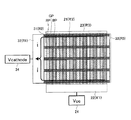
図8に示す配線例では、表示領域Arの外側に、横方向に延伸する複数のカソード配線31の左端に共通接続された、実質的に電流が流れる第1カソードバスライン32と、カソード配線31の右端に共通接続された、カソード配線31の右端の電位差のばらつきを抑制する第2カソードバスライン33とが設けられている。第1カソードバスライン32の中央部に接続された電源端子34が設けられている。
In the wiring example shown in FIG. 8, a first
また、表示領域Arの外側に、縦方向に延伸する複数のアノード配線21の下端に共通接続された、実質的に電流が流れる第1アノードバスライン22と、複数のアノード配線21の上端に共通接続された、アノード配線21の上端の電位差のばらつきを抑制する第2アノードバスライン23とが設けられている。第1アノードバスライン22の中央部に接続された電源端子24が設けられている。
In addition, the first
図8に示す構造においても、カソードバスラインの抵抗値が高いときには、図9に示すような画面上下方向のグレー諧調化を生じるのは図5の場合と同じであるが、この配置によれば図5の第1カソードバスラインよりも狭い配線幅にて諧調化を防止することができる。 Also in the structure shown in FIG. 8, when the resistance value of the cathode bus line is high, the gray gradation in the vertical direction of the screen as shown in FIG. 9 is the same as in FIG. 5, but according to this arrangement, Gradation can be prevented with a wiring width narrower than that of the first cathode bus line in FIG.
図8に示す構造では、片方の第1カソードバスライン32に対してのみ電源端子34を設置する非対称性により、他方の第2カソードバスライン33は電流経路としての寄与が少ない。白表示のとき、カソード配線31を流れる電流は基本的に画面左向きに流れて、左側のバスラインに集められ、電源端子34に至るからである。
In the structure shown in FIG. 8, the other second
第2カソードバスライン33は、カソード配線31の右端における電位差のばらつきを抑えるために設けられており、第2カソードバスライン33の抵抗値をR3とすると、R3<R2(カソード配線31の抵抗値)となるように設定する。
The second
第2の配線例では、第1の配線例(図5参照)と異なり、左右の第1カソードバスライン32の幅を等しくする必要がなく、第2カソードバスライン33の配線幅を極めて狭くしても影響が小さいため、その分さらに額縁幅を狭くすることも可能な点でメリットを有する。
In the second wiring example, unlike the first wiring example (see FIG. 5), it is not necessary to make the widths of the left and right first
図8に示す第2の配線例について、電源端子34を設けた側の必要最低限の第1カソードバスライン32の配線幅を求める。この場合の等価回路は、電源端子34を設けていない側の第2カソードバスライン33の寄与は無視できる程度なので、図10に示すようになる。カソード配線31の両端の電位差V2は次式で与えられる。
For the second wiring example shown in FIG. 8, the minimum wiring width of the first
〔数8〕
V2=R2×i …(1−b)
[Equation 8]
V2 = R2 × i (1-b)
第1カソードバスライン32については、電源端子34がバスライン中央にあるので、第1カソードバスライン32の上半分についての諧調化を防止できればよく、その部分の電位差V1は次式のように求めることができる。
For the first
〔数9〕
V1=(1+2+3+・・・+N/2)×i×R1/N
=N/2×(N/2+1)/2×i×R1/N
=(N+2)/8×i×R1 …(2−b)
[Equation 9]
V1 = (1 + 2 + 3 +... + N / 2) × i × R1 / N
= N / 2 × (N / 2 + 1) / 2 × i × R1 / N
= (N + 2) / 8 * i * R1 (2-b)
画面左右方向、すなわちカソード配線31に沿っての諧調化を生じないのであるから、電位差V1と上記V2の間に下記の関係を満たせば、画面上下方向のグレー諧調化を回避できることになる。
Since gradation in the horizontal direction of the screen, that is, along the
〔数10〕
V1≦V2 …(3−b)
[Equation 10]
V1 ≦ V2 (3-b)
従って、上記式(1−b)、(2−b)より、次の関係が得られる。 Therefore, the following relationship is obtained from the above formulas (1-b) and (2-b).
〔数11〕
R1≦8/(N+2)×R2〜8/N×R2 …(4−b)
[Equation 11]
R1 ≦ 8 / (N + 2) × R2-8 / N × R2 (4-b)
一方、第1カソードバスライン32およびカソード配線31を形成する金属膜のシート抵抗をρとし、第1カソードバスライン32(R1)の配線の長さをL1、幅をW1とし、カソード配線31(R2)の配線の長さをL2、幅をW2とすると、R1、R2は次のように表すことができる。
On the other hand, the sheet resistance of the metal film forming the first
〔数12〕
R1=ρ×L1/W1 …(5−b)
[Equation 12]
R1 = ρ × L1 / W1 (5-b)
〔数13〕
R2=ρ×L2/W2 …(6−b)
[Equation 13]
R2 = ρ × L2 / W2 (6-b)
上記式(4−b)、(5−b)、(6−b)から、第1カソードバスライン32の配線幅について次式を得る。
From the above equations (4-b), (5-b), and (6-b), the following equation is obtained for the wiring width of the first
〔数14〕
W1≧(N+2)/8×L1/L2×W2〜N/8×L1/L2×W2 …(7−b)
[Formula 14]
W1 ≧ (N + 2) / 8 × L1 / L2 × W2 to N / 8 × L1 / L2 × W2 (7−b)
上の手法によれば、式(7−a)の場合よりも狭い第1カソードバスライン32の配線幅で諧調化を防止することができる。たとえば前記QVGA解像度の表示装置に当てはめれば、第1カソードバスライン32の幅W1は約0.23mmとなり、この程度の配線幅により十分諧調化を防止する効果を有することとなる。
According to the above method, gradation can be prevented with the wiring width of the first
第1アノードバスライン22についても、画素に電流を流し込む際に第1アノードバスライン22に生じる電位勾配を小さく押さえることにより、画面左右方向の諧調化を防止する効果がある。これについては細かく説明するまでもなく、第1カソードバスライン32の上記説明がそのまま成り立つ。
The first
ここまでの説明はトップエミッション型を前提としてきたが、最後にボトムエミッション型への適用について述べる。 The explanation so far has been based on the top emission type. Finally, the application to the bottom emission type will be described.
ボトムエミッション型の場合には、図1に示す発光層40からの光が絶縁基板1側に取り出される。従って、絶縁基板1として、透明絶縁基板を採用する。そして、アノード電極20として、ITO等の透明電極を用い、カソード電極30として金属膜等の反射率が高い材料を採用すればよい。
In the case of the bottom emission type, light from the
ボトムエミッション型の場合には、その構造から本来的に画素の発光層面積を広く確保することには適さず、また画素トランジスタ等の形成プロセスを用いて同時に発光層下に付加機能のための回路を設けることにも適さない構造であることを述べた。 In the case of the bottom emission type, the structure is not inherently suitable for securing a large area of the light emitting layer of the pixel, and a circuit for an additional function under the light emitting layer at the same time using a process for forming a pixel transistor or the like. It is said that the structure is not suitable for providing.
しかし、アノード配線21とカソード配線31が直交し、カソード配線31を横配線とする手法は、ボトムエミッション型に適用した場合においても、個々の画素における発光層面積の最大化に寄与する手法である。なお、従来の技術で述べたように、通常ボトムエミッション型のカソード電極(この場合には金属電極)30はストライプ状にする必要はなく、特に制限はない。また、バスラインの低抵抗化の考え方もボトムエミッション型に適用することができるものである。
However, the technique in which the
本発明は、上記の実施形態の説明に限定されない。例えば、R、G、Bの各色画素は、異なる波長の光を発光する発光層40を採用する他、白色光を発光する発光層40上に、R、G、Bの各波長の光を透過するカラーフィルタを設ける構成としてもよい。また、発光層40の整流特性が逆になれば、本実施形態で挙げたアノード、カソードは逆となり、特に限定はない。
その他、本発明の要旨を逸脱しない範囲で、種々の変更が可能である。
The present invention is not limited to the description of the above embodiment. For example, each color pixel of R, G, and B employs a
In addition, various modifications can be made without departing from the scope of the present invention.
1…絶縁基板、2…ゲート電極、3…ゲート絶縁膜、4…半導体層、5…絶縁膜、6…ドレイン電極、8…層間絶縁膜、9…層間絶縁膜、10…TFT、11…TFT、20…アノード電極、21…アノード配線、22…第1アノードバスライン、23…第2アノードバスライン、30…カソード電極、31…カソード配線、32…第1カソードバスライン、33…第2カソードバスライン、40…発光層、RP…赤色画素、GP…緑色画素、BP…青色画素、Ar…表示領域、Cs…キャパシタ
DESCRIPTION OF SYMBOLS 1 ... Insulating substrate, 2 ... Gate electrode, 3 ... Gate insulating film, 4 ... Semiconductor layer, 5 ... Insulating film, 6 ... Drain electrode, 8 ... Interlayer insulating film, 9 ... Interlayer insulating film, 10 ... TFT, 11 ... TFT , 20 ... anode electrode, 21 ... anode wiring, 22 ... first anode bus line, 23 ... second anode bus line, 30 ... cathode electrode, 31 ... cathode wiring, 32 ... first cathode bus line, 33 ... second
Claims (4)
前記第1電極に対向して設けられた透明な第2電極と、
前記第1電極と前記第2電極との間に挟まれた発光層と、
を有する発光素子が第1方向および前記第1方向と垂直である第2方向にマトリックス状に配置され、前記発光層からの光が前記基板とは反対側に取り出される表示領域を有し、
前記表示領域内において、
単一の金属層により形成され、前記第1方向に延伸し、当該第1方向に配列した複数の前記第1電極に電気的に共通接続された複数の第1電極配線と、
前記第1電極と同一層に前記第1電極配線に対し間隔を隔てて配置され、前記第2方向に延伸し、前記第2方向に配列した複数の前記第2電極に電気的に共通接続された複数の第2電極配線と、
前記表示領域の外側に、
前記第1方向に延伸する複数の前記第1電極配線に共通接続された第1バスラインと、
前記第2方向に延伸する複数の前記第2電極配線に共通接続され、前記第1バスラインとは接続されていない第2バスラインと
を有し、
前記第2バスラインは、
前記第2方向に延伸する複数の前記第2電極配線の一方側に共通接続された、実質的に電流が流れる第3バスラインと、
前記第2方向に延伸する複数の前記第2電極配線の他方側に共通接続された、前記第2電極配線の電位差のばらつきを抑制する第4バスラインと
を含み、
前記第3バスラインの抵抗値および前記第4バスラインの抵抗値が下記式を満足するように規定されている
表示装置。
R1≦8×R2/N
R3<R2
但し、上記式において、R1は第3バスラインの抵抗値であり、R2は第2電極配線の抵抗値であり、R3は第4バスラインの抵抗値であり、Nは第2電極配線の本数である。 A first electrode formed on a substrate and defining a light emitting region;
A transparent second electrode provided opposite to the first electrode;
A light emitting layer sandwiched between the first electrode and the second electrode;
A light-emitting element having a display region in which light from the light-emitting layer is extracted on the side opposite to the substrate, arranged in a matrix in a first direction and a second direction perpendicular to the first direction;
Within the display area,
A plurality of first electrode wires formed of a single metal layer , extending in the first direction and electrically connected in common to the plurality of first electrodes arranged in the first direction;
The first electrode is disposed on the same layer as the first electrode wiring, spaced from the first electrode wiring, extends in the second direction, and is electrically connected in common to the plurality of second electrodes arranged in the second direction. A plurality of second electrode wirings;
Outside the display area,
A first bus line commonly connected to the plurality of first electrode wires extending in the first direction;
A second bus line that is commonly connected to the plurality of second electrode lines extending in the second direction and not connected to the first bus line;
The second bus line is
A third bus line that is commonly connected to one side of the plurality of second electrode wires extending in the second direction and through which a substantially current flows;
A fourth bus line that is commonly connected to the other side of the plurality of second electrode wirings extending in the second direction and suppresses variation in potential difference of the second electrode wirings;
Including
The resistance value of the third bus line and the resistance value of the fourth bus line are defined so as to satisfy the following expression.
Display device.
R1 ≦ 8 × R2 / N
R3 <R2
In the above formula, R1 is the resistance value of the third bus line, R2 is the resistance value of the second electrode wiring, R3 is the resistance value of the fourth bus line, and N is the number of the second electrode wirings. It is.
請求項1記載の表示装置。 The display device of claim 1, further comprising the connected power terminal to the central portion of the third bus lines.
前記第1電極に対向して設けられた透明な第2電極と、
前記第1電極と前記第2電極との間に挟まれた発光層と、
を有する発光素子が第1方向および前記第1方向と垂直である第2方向にマトリックス状に配置され、前記発光層からの光が前記基板とは反対側に取り出される表示領域を有し、
前記表示領域内において、
単一の金属層により形成され、前記第1方向に延伸し、当該第1方向に配列した複数の前記第1電極に電気的に共通接続された複数の第1電極配線と、
前記第1電極度同一層に前記第1電極配線に対し間隔を隔てて配置され、前記第2方向に延伸し、前記第2方向に配列した複数の前記第2電極に電気的に共通接続された複数の第2電極配線と、
前記表示領域の外側に、
前記第1方向に延伸する複数の前記第1電極配線に共通接続された第1バスラインと、
前記第2方向に延伸する複数の前記第2電極配線に共通接続され、前記第1バスラインとは接続されていない第2バスラインと
を有し、
前記第2バスラインは、
前記第2方向に延伸する複数の前記第2電極配線の一方側に共通接続された、実質的に電流が流れる第3バスラインと、
前記第2方向に延伸する複数の前記第2電極配線の他方側に共通接続された、前記第2電極配線の電位差のばらつきを抑制する第4バスラインと
を含み、
前記第2バスラインの抵抗値が下記式を満足するように規定されている
表示装置。
R1≦R2/(N−1)
但し、上記式において、R1は第2バスラインの抵抗値であり、R2は第2電極配線の抵抗値であり、Nは第2電極配線の本数である。 A first electrode formed on a substrate and defining a light emitting region;
A transparent second electrode provided opposite to the first electrode;
A light emitting layer sandwiched between the first electrode and the second electrode;
A light-emitting element having a display region in which light from the light-emitting layer is extracted on the side opposite to the substrate, arranged in a matrix in a first direction and a second direction perpendicular to the first direction;
Within the display area,
A plurality of first electrode wires formed of a single metal layer , extending in the first direction and electrically connected in common to the plurality of first electrodes arranged in the first direction;
The first electrode degree is disposed on the same layer at a distance from the first electrode wiring, extends in the second direction, and is electrically connected in common to the plurality of second electrodes arranged in the second direction. A plurality of second electrode wirings;
Outside the display area,
A first bus line commonly connected to the plurality of first electrode wires extending in the first direction;
A second bus line that is commonly connected to the plurality of second electrode lines extending in the second direction and not connected to the first bus line;
The second bus line is
A third bus line that is commonly connected to one side of the plurality of second electrode wires extending in the second direction and through which a substantially current flows;
A fourth bus line that is commonly connected to the other side of the plurality of second electrode wirings extending in the second direction and suppresses variation in potential difference of the second electrode wirings;
Including
The resistance value of the second bus line is defined to satisfy the following formula:
Display device.
R1 ≦ R2 / (N-1)
In the above equation, R1 is the resistance value of the second bus line, R2 is the resistance value of the second electrode wiring, and N is the number of second electrode wirings.
請求項3記載の表示装置。 The display device according to claim 3 , further comprising two power supply terminals connected to each of the third bus line and the fourth bus line.
Priority Applications (2)
| Application Number | Priority Date | Filing Date | Title |
|---|---|---|---|
| JP2004145873A JP4148182B2 (en) | 2004-05-17 | 2004-05-17 | Display device |
| US11/108,738 US7612495B2 (en) | 2004-05-17 | 2005-04-19 | Display device |
Applications Claiming Priority (1)
| Application Number | Priority Date | Filing Date | Title |
|---|---|---|---|
| JP2004145873A JP4148182B2 (en) | 2004-05-17 | 2004-05-17 | Display device |
Publications (2)
| Publication Number | Publication Date |
|---|---|
| JP2005326704A JP2005326704A (en) | 2005-11-24 |
| JP4148182B2 true JP4148182B2 (en) | 2008-09-10 |
Family
ID=35308771
Family Applications (1)
| Application Number | Title | Priority Date | Filing Date |
|---|---|---|---|
| JP2004145873A Expired - Fee Related JP4148182B2 (en) | 2004-05-17 | 2004-05-17 | Display device |
Country Status (2)
| Country | Link |
|---|---|
| US (1) | US7612495B2 (en) |
| JP (1) | JP4148182B2 (en) |
Families Citing this family (25)
| Publication number | Priority date | Publication date | Assignee | Title |
|---|---|---|---|---|
| US20060091397A1 (en) * | 2004-11-04 | 2006-05-04 | Kengo Akimoto | Display device and method for manufacturing the same |
| US7990054B2 (en) * | 2005-12-19 | 2011-08-02 | Koninklijke Philips Electronics N.V. | Organic LED device with electrodes having reduced resistance |
| CN101401226A (en) * | 2006-03-09 | 2009-04-01 | 皇家飞利浦电子股份有限公司 | Lighting elements with segmented electrodes |
| US7573112B2 (en) * | 2006-04-14 | 2009-08-11 | Allegro Microsystems, Inc. | Methods and apparatus for sensor having capacitor on chip |
| US7687882B2 (en) | 2006-04-14 | 2010-03-30 | Allegro Microsystems, Inc. | Methods and apparatus for integrated circuit having multiple dies with at least one on chip capacitor |
| US20080013298A1 (en) | 2006-07-14 | 2008-01-17 | Nirmal Sharma | Methods and apparatus for passive attachment of components for integrated circuits |
| KR20090010826A (en) * | 2007-07-24 | 2009-01-30 | 삼성전자주식회사 | Display device and driving method of display device |
| JP5251034B2 (en) * | 2007-08-15 | 2013-07-31 | ソニー株式会社 | Display device and electronic device |
| JP5007246B2 (en) * | 2008-01-31 | 2012-08-22 | 三菱電機株式会社 | Organic electroluminescent display device and manufacturing method thereof |
| US8093670B2 (en) | 2008-07-24 | 2012-01-10 | Allegro Microsystems, Inc. | Methods and apparatus for integrated circuit having on chip capacitor with eddy current reductions |
| US20100052424A1 (en) * | 2008-08-26 | 2010-03-04 | Taylor William P | Methods and apparatus for integrated circuit having integrated energy storage device |
| WO2013000164A1 (en) * | 2011-06-30 | 2013-01-03 | 海洋王照明科技股份有限公司 | Top-emitting organic electroluminescent device and manufacturing method thereof |
| CN103548169A (en) * | 2011-06-30 | 2014-01-29 | 海洋王照明科技股份有限公司 | Top-emitting flexible organic light emission diode device and preparation method thereof |
| US9313835B2 (en) * | 2011-09-30 | 2016-04-12 | Idemitsu Kosan Co., Ltd. | Planar light emitting device |
| US8629539B2 (en) | 2012-01-16 | 2014-01-14 | Allegro Microsystems, Llc | Methods and apparatus for magnetic sensor having non-conductive die paddle |
| US10234513B2 (en) | 2012-03-20 | 2019-03-19 | Allegro Microsystems, Llc | Magnetic field sensor integrated circuit with integral ferromagnetic material |
| US9494660B2 (en) | 2012-03-20 | 2016-11-15 | Allegro Microsystems, Llc | Integrated circuit package having a split lead frame |
| US9812588B2 (en) | 2012-03-20 | 2017-11-07 | Allegro Microsystems, Llc | Magnetic field sensor integrated circuit with integral ferromagnetic material |
| US9666788B2 (en) | 2012-03-20 | 2017-05-30 | Allegro Microsystems, Llc | Integrated circuit package having a split lead frame |
| US9411025B2 (en) | 2013-04-26 | 2016-08-09 | Allegro Microsystems, Llc | Integrated circuit package having a split lead frame and a magnet |
| KR102090703B1 (en) * | 2013-05-21 | 2020-04-16 | 삼성디스플레이 주식회사 | Organinc light emitting display device and manufacturing method for the same |
| KR102237135B1 (en) * | 2014-07-14 | 2021-04-08 | 삼성디스플레이 주식회사 | Organic light emitting display device and method of manufacturing an organic light emitting display device |
| US10411498B2 (en) | 2015-10-21 | 2019-09-10 | Allegro Microsystems, Llc | Apparatus and methods for extending sensor integrated circuit operation through a power disturbance |
| US10978897B2 (en) | 2018-04-02 | 2021-04-13 | Allegro Microsystems, Llc | Systems and methods for suppressing undesirable voltage supply artifacts |
| US10991644B2 (en) | 2019-08-22 | 2021-04-27 | Allegro Microsystems, Llc | Integrated circuit package having a low profile |
Family Cites Families (22)
| Publication number | Priority date | Publication date | Assignee | Title |
|---|---|---|---|---|
| US4689522A (en) * | 1985-12-03 | 1987-08-25 | The United States Of America As Represented By The Administator Of The National Aeronautics And Space Administration | Flat-panel, full-color, electroluminescent display |
| FR2645998B1 (en) * | 1989-04-12 | 1991-06-07 | France Etat | ELECTROLUMINESCENT DISPLAY WITH MEMORY AND SPECIFICALLY CONFIGURED ELECTRODES |
| JPH09115673A (en) * | 1995-10-13 | 1997-05-02 | Sony Corp | Light emission element or device, and driving method thereof |
| JP2001109397A (en) * | 1999-10-04 | 2001-04-20 | Sanyo Electric Co Ltd | El display device |
| JP4593740B2 (en) * | 2000-07-28 | 2010-12-08 | ルネサスエレクトロニクス株式会社 | Display device |
| JP2002108252A (en) * | 2000-09-29 | 2002-04-10 | Sanyo Electric Co Ltd | Electro-luminescence display panel |
| JP2002196352A (en) * | 2000-12-07 | 2002-07-12 | Koninkl Philips Electronics Nv | Liquid crystal display device having spare wiring |
| JP2002318556A (en) * | 2001-04-20 | 2002-10-31 | Toshiba Corp | Active matrix type planar display device and manufacturing method therefor |
| US6664730B2 (en) * | 2001-07-09 | 2003-12-16 | Universal Display Corporation | Electrode structure of el device |
| JP4887585B2 (en) * | 2001-08-24 | 2012-02-29 | パナソニック株式会社 | Display panel and information display device using the same |
| JP4310984B2 (en) * | 2002-02-06 | 2009-08-12 | 株式会社日立製作所 | Organic light emitting display |
| JP4490650B2 (en) * | 2002-04-26 | 2010-06-30 | 東芝モバイルディスプレイ株式会社 | EL display device driving method and EL display device |
| JP4005410B2 (en) * | 2002-05-15 | 2007-11-07 | 株式会社 日立ディスプレイズ | Image display device |
| JP4165145B2 (en) * | 2002-08-07 | 2008-10-15 | 株式会社日立製作所 | Organic light emitting display |
| US20040043140A1 (en) * | 2002-08-21 | 2004-03-04 | Ramesh Jagannathan | Solid state lighting using compressed fluid coatings |
| JP3977299B2 (en) * | 2002-09-18 | 2007-09-19 | セイコーエプソン株式会社 | Electro-optical device, matrix substrate, and electronic apparatus |
| KR20040025383A (en) * | 2002-09-19 | 2004-03-24 | 삼성에스디아이 주식회사 | Organic electro luminescence display device and manufacturing of the same |
| JP3922374B2 (en) * | 2002-09-25 | 2007-05-30 | セイコーエプソン株式会社 | Electro-optical device, matrix substrate, and electronic apparatus |
| US6936407B2 (en) * | 2003-02-28 | 2005-08-30 | Osram Opto Semiconductors Gmbh | Thin-film electronic device module |
| KR100490322B1 (en) * | 2003-04-07 | 2005-05-17 | 삼성전자주식회사 | Organic electro-luminescent display |
| JP3922228B2 (en) * | 2003-08-28 | 2007-05-30 | セイコーエプソン株式会社 | Light emitting device |
| US7027044B2 (en) * | 2004-02-20 | 2006-04-11 | Au Optronics Corporation | Power line arrangement for electroluminescence display devices |
-
2004
- 2004-05-17 JP JP2004145873A patent/JP4148182B2/en not_active Expired - Fee Related
-
2005
- 2005-04-19 US US11/108,738 patent/US7612495B2/en not_active Expired - Fee Related
Also Published As
| Publication number | Publication date |
|---|---|
| US20050253507A1 (en) | 2005-11-17 |
| JP2005326704A (en) | 2005-11-24 |
| US7612495B2 (en) | 2009-11-03 |
Similar Documents
| Publication | Publication Date | Title |
|---|---|---|
| JP4148182B2 (en) | Display device | |
| US9934724B2 (en) | Display device | |
| JP4273809B2 (en) | Electro-optical device and electronic apparatus | |
| JP4593740B2 (en) | Display device | |
| US7190122B2 (en) | OLED display with improved active matrix circuitry | |
| US7205967B2 (en) | Display apparatus and drive method therefor | |
| US20150372071A1 (en) | Display module | |
| JP5107546B2 (en) | Display device | |
| US11678555B2 (en) | Display device having transmissive area | |
| CN109994513B (en) | Display device and method of manufacturing the same | |
| US20110241036A1 (en) | Light-emitting apparatus | |
| CN110783373A (en) | Display device | |
| US20220101792A1 (en) | Display apparatus | |
| CN112703606A (en) | Organic light emitting display device | |
| JP6056072B2 (en) | Display device | |
| JP7261071B2 (en) | Display device | |
| JP2004356052A (en) | Electroluminescent display panel | |
| JP4122949B2 (en) | Electro-optical device, active matrix substrate, and electronic apparatus | |
| JP4193451B2 (en) | Electro-optical device and electronic apparatus | |
| JP4815727B2 (en) | EL display device and electronic apparatus | |
| JP7312697B2 (en) | Displays and electronics | |
| JP6056073B2 (en) | Display device | |
| US20220319412A1 (en) | Display device | |
| JP2004117690A (en) | Electrooptical device and electronic equipment | |
| CN116997855A (en) | Array substrate and display device |
Legal Events
| Date | Code | Title | Description |
|---|---|---|---|
| A977 | Report on retrieval |
Free format text: JAPANESE INTERMEDIATE CODE: A971007 Effective date: 20071025 |
|
| A131 | Notification of reasons for refusal |
Free format text: JAPANESE INTERMEDIATE CODE: A131 Effective date: 20071106 |
|
| A521 | Request for written amendment filed |
Free format text: JAPANESE INTERMEDIATE CODE: A523 Effective date: 20080107 |
|
| A131 | Notification of reasons for refusal |
Free format text: JAPANESE INTERMEDIATE CODE: A131 Effective date: 20080226 |
|
| A521 | Request for written amendment filed |
Free format text: JAPANESE INTERMEDIATE CODE: A523 Effective date: 20080425 |
|
| TRDD | Decision of grant or rejection written | ||
| A01 | Written decision to grant a patent or to grant a registration (utility model) |
Free format text: JAPANESE INTERMEDIATE CODE: A01 Effective date: 20080603 |
|
| A01 | Written decision to grant a patent or to grant a registration (utility model) |
Free format text: JAPANESE INTERMEDIATE CODE: A01 |
|
| A61 | First payment of annual fees (during grant procedure) |
Free format text: JAPANESE INTERMEDIATE CODE: A61 Effective date: 20080616 |
|
| FPAY | Renewal fee payment (event date is renewal date of database) |
Free format text: PAYMENT UNTIL: 20110704 Year of fee payment: 3 |
|
| FPAY | Renewal fee payment (event date is renewal date of database) |
Free format text: PAYMENT UNTIL: 20110704 Year of fee payment: 3 |
|
| FPAY | Renewal fee payment (event date is renewal date of database) |
Free format text: PAYMENT UNTIL: 20110704 Year of fee payment: 3 |
|
| FPAY | Renewal fee payment (event date is renewal date of database) |
Free format text: PAYMENT UNTIL: 20120704 Year of fee payment: 4 |
|
| FPAY | Renewal fee payment (event date is renewal date of database) |
Free format text: PAYMENT UNTIL: 20120704 Year of fee payment: 4 |
|
| FPAY | Renewal fee payment (event date is renewal date of database) |
Free format text: PAYMENT UNTIL: 20130704 Year of fee payment: 5 |
|
| R250 | Receipt of annual fees |
Free format text: JAPANESE INTERMEDIATE CODE: R250 |
|
| R250 | Receipt of annual fees |
Free format text: JAPANESE INTERMEDIATE CODE: R250 |
|
| S111 | Request for change of ownership or part of ownership |
Free format text: JAPANESE INTERMEDIATE CODE: R313111 |
|
| R350 | Written notification of registration of transfer |
Free format text: JAPANESE INTERMEDIATE CODE: R350 |
|
| R250 | Receipt of annual fees |
Free format text: JAPANESE INTERMEDIATE CODE: R250 |
|
| R250 | Receipt of annual fees |
Free format text: JAPANESE INTERMEDIATE CODE: R250 |
|
| R250 | Receipt of annual fees |
Free format text: JAPANESE INTERMEDIATE CODE: R250 |
|
| LAPS | Cancellation because of no payment of annual fees |