JP5007246B2 - Organic electroluminescent display device and manufacturing method thereof - Google Patents
Organic electroluminescent display device and manufacturing method thereof Download PDFInfo
- Publication number
- JP5007246B2 JP5007246B2 JP2008020501A JP2008020501A JP5007246B2 JP 5007246 B2 JP5007246 B2 JP 5007246B2 JP 2008020501 A JP2008020501 A JP 2008020501A JP 2008020501 A JP2008020501 A JP 2008020501A JP 5007246 B2 JP5007246 B2 JP 5007246B2
- Authority
- JP
- Japan
- Prior art keywords
- film
- alloy film
- display device
- organic electroluminescent
- anode
- Prior art date
- Legal status (The legal status is an assumption and is not a legal conclusion. Google has not performed a legal analysis and makes no representation as to the accuracy of the status listed.)
- Active
Links
- 238000004519 manufacturing process Methods 0.000 title claims description 23
- 239000010408 film Substances 0.000 claims description 345
- 229910000838 Al alloy Inorganic materials 0.000 claims description 105
- 229910052760 oxygen Inorganic materials 0.000 claims description 36
- QVGXLLKOCUKJST-UHFFFAOYSA-N atomic oxygen Chemical compound [O] QVGXLLKOCUKJST-UHFFFAOYSA-N 0.000 claims description 34
- 239000001301 oxygen Substances 0.000 claims description 34
- 239000012535 impurity Substances 0.000 claims description 32
- 239000000758 substrate Substances 0.000 claims description 27
- 238000000034 method Methods 0.000 claims description 23
- 239000000203 mixture Substances 0.000 claims description 20
- 229910052782 aluminium Inorganic materials 0.000 claims description 17
- 239000007789 gas Substances 0.000 claims description 16
- 229910052759 nickel Inorganic materials 0.000 claims description 16
- XAGFODPZIPBFFR-UHFFFAOYSA-N aluminium Chemical compound [Al] XAGFODPZIPBFFR-UHFFFAOYSA-N 0.000 claims description 15
- XKRFYHLGVUSROY-UHFFFAOYSA-N Argon Chemical compound [Ar] XKRFYHLGVUSROY-UHFFFAOYSA-N 0.000 claims description 12
- 239000010409 thin film Substances 0.000 claims description 12
- 238000004544 sputter deposition Methods 0.000 claims description 11
- 229910052742 iron Inorganic materials 0.000 claims description 8
- 238000005477 sputtering target Methods 0.000 claims description 7
- 229910052684 Cerium Inorganic materials 0.000 claims description 6
- 229910052692 Dysprosium Inorganic materials 0.000 claims description 6
- 229910052691 Erbium Inorganic materials 0.000 claims description 6
- 229910052688 Gadolinium Inorganic materials 0.000 claims description 6
- 229910052689 Holmium Inorganic materials 0.000 claims description 6
- 229910052779 Neodymium Inorganic materials 0.000 claims description 6
- 229910052777 Praseodymium Inorganic materials 0.000 claims description 6
- 229910052772 Samarium Inorganic materials 0.000 claims description 6
- 229910052771 Terbium Inorganic materials 0.000 claims description 6
- 229910052786 argon Inorganic materials 0.000 claims description 6
- 238000010030 laminating Methods 0.000 claims description 6
- 229910052746 lanthanum Inorganic materials 0.000 claims description 6
- 229910052761 rare earth metal Inorganic materials 0.000 claims description 6
- 229910052727 yttrium Inorganic materials 0.000 claims description 6
- 229910044991 metal oxide Inorganic materials 0.000 claims description 4
- 150000004706 metal oxides Chemical class 0.000 claims description 4
- 230000005684 electric field Effects 0.000 claims 1
- 239000010410 layer Substances 0.000 description 116
- PXHVJJICTQNCMI-UHFFFAOYSA-N nickel Substances [Ni] PXHVJJICTQNCMI-UHFFFAOYSA-N 0.000 description 37
- 239000011229 interlayer Substances 0.000 description 23
- 229910021420 polycrystalline silicon Inorganic materials 0.000 description 17
- 229910052751 metal Inorganic materials 0.000 description 16
- 239000002184 metal Substances 0.000 description 16
- 229920005591 polysilicon Polymers 0.000 description 16
- 239000000463 material Substances 0.000 description 13
- QTBSBXVTEAMEQO-UHFFFAOYSA-N Acetic acid Chemical compound CC(O)=O QTBSBXVTEAMEQO-UHFFFAOYSA-N 0.000 description 12
- MUBZPKHOEPUJKR-UHFFFAOYSA-N Oxalic acid Chemical compound OC(=O)C(O)=O MUBZPKHOEPUJKR-UHFFFAOYSA-N 0.000 description 12
- 238000000926 separation method Methods 0.000 description 12
- XLOMVQKBTHCTTD-UHFFFAOYSA-N Zinc monoxide Chemical compound [Zn]=O XLOMVQKBTHCTTD-UHFFFAOYSA-N 0.000 description 11
- 229910021417 amorphous silicon Inorganic materials 0.000 description 11
- 238000002347 injection Methods 0.000 description 11
- 239000007924 injection Substances 0.000 description 11
- 229910004298 SiO 2 Inorganic materials 0.000 description 10
- 229910052723 transition metal Inorganic materials 0.000 description 9
- 150000003624 transition metals Chemical class 0.000 description 9
- NBIIXXVUZAFLBC-UHFFFAOYSA-N Phosphoric acid Chemical compound OP(O)(O)=O NBIIXXVUZAFLBC-UHFFFAOYSA-N 0.000 description 8
- 230000007547 defect Effects 0.000 description 8
- 238000005530 etching Methods 0.000 description 8
- 230000005525 hole transport Effects 0.000 description 8
- 230000000694 effects Effects 0.000 description 7
- 229910003437 indium oxide Inorganic materials 0.000 description 7
- PJXISJQVUVHSOJ-UHFFFAOYSA-N indium(iii) oxide Chemical group [O-2].[O-2].[O-2].[In+3].[In+3] PJXISJQVUVHSOJ-UHFFFAOYSA-N 0.000 description 7
- 230000008569 process Effects 0.000 description 7
- 230000009467 reduction Effects 0.000 description 7
- 230000007423 decrease Effects 0.000 description 6
- 239000012528 membrane Substances 0.000 description 6
- 238000001579 optical reflectometry Methods 0.000 description 6
- 238000005546 reactive sputtering Methods 0.000 description 6
- 239000011347 resin Substances 0.000 description 6
- 229920005989 resin Polymers 0.000 description 6
- 238000007789 sealing Methods 0.000 description 6
- 239000000243 solution Substances 0.000 description 6
- 229910001151 AlNi Inorganic materials 0.000 description 5
- 229910045601 alloy Inorganic materials 0.000 description 5
- 239000000956 alloy Substances 0.000 description 5
- 238000006243 chemical reaction Methods 0.000 description 5
- 230000000052 comparative effect Effects 0.000 description 5
- 238000005401 electroluminescence Methods 0.000 description 5
- 238000000206 photolithography Methods 0.000 description 5
- 239000011787 zinc oxide Substances 0.000 description 5
- UFHFLCQGNIYNRP-UHFFFAOYSA-N Hydrogen Chemical compound [H][H] UFHFLCQGNIYNRP-UHFFFAOYSA-N 0.000 description 4
- GRYLNZFGIOXLOG-UHFFFAOYSA-N Nitric acid Chemical compound O[N+]([O-])=O GRYLNZFGIOXLOG-UHFFFAOYSA-N 0.000 description 4
- 229910000147 aluminium phosphate Inorganic materials 0.000 description 4
- 230000015572 biosynthetic process Effects 0.000 description 4
- 230000006866 deterioration Effects 0.000 description 4
- 239000001257 hydrogen Substances 0.000 description 4
- 229910052739 hydrogen Inorganic materials 0.000 description 4
- 239000011159 matrix material Substances 0.000 description 4
- 239000007769 metal material Substances 0.000 description 4
- 229910017604 nitric acid Inorganic materials 0.000 description 4
- 229910052757 nitrogen Inorganic materials 0.000 description 4
- 235000006408 oxalic acid Nutrition 0.000 description 4
- 230000007704 transition Effects 0.000 description 4
- ZOXJGFHDIHLPTG-UHFFFAOYSA-N Boron Chemical compound [B] ZOXJGFHDIHLPTG-UHFFFAOYSA-N 0.000 description 3
- 229910006404 SnO 2 Inorganic materials 0.000 description 3
- 238000000137 annealing Methods 0.000 description 3
- 230000008901 benefit Effects 0.000 description 3
- 229910052796 boron Inorganic materials 0.000 description 3
- 239000004020 conductor Substances 0.000 description 3
- 238000010586 diagram Methods 0.000 description 3
- 230000003287 optical effect Effects 0.000 description 3
- 238000005268 plasma chemical vapour deposition Methods 0.000 description 3
- 238000002310 reflectometry Methods 0.000 description 3
- XOLBLPGZBRYERU-UHFFFAOYSA-N tin dioxide Chemical compound O=[Sn]=O XOLBLPGZBRYERU-UHFFFAOYSA-N 0.000 description 3
- 229910001887 tin oxide Inorganic materials 0.000 description 3
- 238000002834 transmittance Methods 0.000 description 3
- IJGRMHOSHXDMSA-UHFFFAOYSA-N Atomic nitrogen Chemical compound N#N IJGRMHOSHXDMSA-UHFFFAOYSA-N 0.000 description 2
- 239000004642 Polyimide Substances 0.000 description 2
- PNEYBMLMFCGWSK-UHFFFAOYSA-N aluminium oxide Inorganic materials [O-2].[O-2].[O-2].[Al+3].[Al+3] PNEYBMLMFCGWSK-UHFFFAOYSA-N 0.000 description 2
- -1 aromatic hydrazones Chemical group 0.000 description 2
- 230000008859 change Effects 0.000 description 2
- 229910052804 chromium Inorganic materials 0.000 description 2
- 239000011248 coating agent Substances 0.000 description 2
- 238000000576 coating method Methods 0.000 description 2
- ZYGHJZDHTFUPRJ-UHFFFAOYSA-N coumarin Chemical compound C1=CC=C2OC(=O)C=CC2=C1 ZYGHJZDHTFUPRJ-UHFFFAOYSA-N 0.000 description 2
- 238000000151 deposition Methods 0.000 description 2
- 230000008021 deposition Effects 0.000 description 2
- 238000002474 experimental method Methods 0.000 description 2
- 239000011521 glass Substances 0.000 description 2
- 238000010438 heat treatment Methods 0.000 description 2
- 238000005224 laser annealing Methods 0.000 description 2
- 229910052750 molybdenum Inorganic materials 0.000 description 2
- 239000000615 nonconductor Substances 0.000 description 2
- 239000011368 organic material Substances 0.000 description 2
- 229920001721 polyimide Polymers 0.000 description 2
- 239000000047 product Substances 0.000 description 2
- 239000000376 reactant Substances 0.000 description 2
- 230000009257 reactivity Effects 0.000 description 2
- 239000004065 semiconductor Substances 0.000 description 2
- 229910052709 silver Inorganic materials 0.000 description 2
- NGQSLSMAEVWNPU-YTEMWHBBSA-N 1,2-bis[(e)-2-phenylethenyl]benzene Chemical compound C=1C=CC=CC=1/C=C/C1=CC=CC=C1\C=C\C1=CC=CC=C1 NGQSLSMAEVWNPU-YTEMWHBBSA-N 0.000 description 1
- KLCLIOISYBHYDZ-UHFFFAOYSA-N 1,4,4-triphenylbuta-1,3-dienylbenzene Chemical compound C=1C=CC=CC=1C(C=1C=CC=CC=1)=CC=C(C=1C=CC=CC=1)C1=CC=CC=C1 KLCLIOISYBHYDZ-UHFFFAOYSA-N 0.000 description 1
- KYGSXEYUWRFVNY-UHFFFAOYSA-N 2-pyran-2-ylidenepropanedinitrile Chemical class N#CC(C#N)=C1OC=CC=C1 KYGSXEYUWRFVNY-UHFFFAOYSA-N 0.000 description 1
- 229910001316 Ag alloy Inorganic materials 0.000 description 1
- NRCMAYZCPIVABH-UHFFFAOYSA-N Quinacridone Chemical compound N1C2=CC=CC=C2C(=O)C2=C1C=C1C(=O)C3=CC=CC=C3NC1=C2 NRCMAYZCPIVABH-UHFFFAOYSA-N 0.000 description 1
- VVTSZOCINPYFDP-UHFFFAOYSA-N [O].[Ar] Chemical compound [O].[Ar] VVTSZOCINPYFDP-UHFFFAOYSA-N 0.000 description 1
- NIXOWILDQLNWCW-UHFFFAOYSA-N acrylic acid group Chemical group C(C=C)(=O)O NIXOWILDQLNWCW-UHFFFAOYSA-N 0.000 description 1
- 230000002411 adverse Effects 0.000 description 1
- 125000003118 aryl group Chemical group 0.000 description 1
- 239000003054 catalyst Substances 0.000 description 1
- 238000005229 chemical vapour deposition Methods 0.000 description 1
- 229960000956 coumarin Drugs 0.000 description 1
- 235000001671 coumarin Nutrition 0.000 description 1
- 150000004775 coumarins Chemical class 0.000 description 1
- 239000013078 crystal Substances 0.000 description 1
- 230000003247 decreasing effect Effects 0.000 description 1
- 230000002349 favourable effect Effects 0.000 description 1
- 238000011835 investigation Methods 0.000 description 1
- 150000002500 ions Chemical class 0.000 description 1
- 125000000040 m-tolyl group Chemical group [H]C1=C([H])C(*)=C([H])C(=C1[H])C([H])([H])[H] 0.000 description 1
- 238000005259 measurement Methods 0.000 description 1
- 238000002156 mixing Methods 0.000 description 1
- 150000004866 oxadiazoles Chemical class 0.000 description 1
- 239000002245 particle Substances 0.000 description 1
- 238000000059 patterning Methods 0.000 description 1
- 230000035699 permeability Effects 0.000 description 1
- 239000002244 precipitate Substances 0.000 description 1
- 150000003219 pyrazolines Chemical class 0.000 description 1
- 239000010453 quartz Substances 0.000 description 1
- 239000003870 refractory metal Substances 0.000 description 1
- VYPSYNLAJGMNEJ-UHFFFAOYSA-N silicon dioxide Inorganic materials O=[Si]=O VYPSYNLAJGMNEJ-UHFFFAOYSA-N 0.000 description 1
- 239000002356 single layer Substances 0.000 description 1
- 150000001629 stilbenes Chemical class 0.000 description 1
- 235000021286 stilbenes Nutrition 0.000 description 1
- 239000000126 substance Substances 0.000 description 1
- 238000010301 surface-oxidation reaction Methods 0.000 description 1
- 229940042055 systemic antimycotics triazole derivative Drugs 0.000 description 1
- 125000005259 triarylamine group Chemical group 0.000 description 1
- 238000007740 vapor deposition Methods 0.000 description 1
Images


Classifications
-
- H—ELECTRICITY
- H10—SEMICONDUCTOR DEVICES; ELECTRIC SOLID-STATE DEVICES NOT OTHERWISE PROVIDED FOR
- H10K—ORGANIC ELECTRIC SOLID-STATE DEVICES
- H10K10/00—Organic devices specially adapted for rectifying, amplifying, oscillating or switching; Organic capacitors or resistors having a potential-jump barrier or a surface barrier
- H10K10/80—Constructional details
- H10K10/82—Electrodes
- H10K10/84—Ohmic electrodes, e.g. source or drain electrodes
-
- H—ELECTRICITY
- H10—SEMICONDUCTOR DEVICES; ELECTRIC SOLID-STATE DEVICES NOT OTHERWISE PROVIDED FOR
- H10K—ORGANIC ELECTRIC SOLID-STATE DEVICES
- H10K50/00—Organic light-emitting devices
- H10K50/80—Constructional details
- H10K50/805—Electrodes
- H10K50/81—Anodes
- H10K50/818—Reflective anodes, e.g. ITO combined with thick metallic layers
-
- H—ELECTRICITY
- H10—SEMICONDUCTOR DEVICES; ELECTRIC SOLID-STATE DEVICES NOT OTHERWISE PROVIDED FOR
- H10K—ORGANIC ELECTRIC SOLID-STATE DEVICES
- H10K59/00—Integrated devices, or assemblies of multiple devices, comprising at least one organic light-emitting element covered by group H10K50/00
- H10K59/80—Constructional details
- H10K59/805—Electrodes
- H10K59/8051—Anodes
- H10K59/80518—Reflective anodes, e.g. ITO combined with thick metallic layers
-
- H—ELECTRICITY
- H10—SEMICONDUCTOR DEVICES; ELECTRIC SOLID-STATE DEVICES NOT OTHERWISE PROVIDED FOR
- H10K—ORGANIC ELECTRIC SOLID-STATE DEVICES
- H10K2102/00—Constructional details relating to the organic devices covered by this subclass
- H10K2102/10—Transparent electrodes, e.g. using graphene
- H10K2102/101—Transparent electrodes, e.g. using graphene comprising transparent conductive oxides [TCO]
- H10K2102/103—Transparent electrodes, e.g. using graphene comprising transparent conductive oxides [TCO] comprising indium oxides, e.g. ITO
-
- H—ELECTRICITY
- H10—SEMICONDUCTOR DEVICES; ELECTRIC SOLID-STATE DEVICES NOT OTHERWISE PROVIDED FOR
- H10K—ORGANIC ELECTRIC SOLID-STATE DEVICES
- H10K59/00—Integrated devices, or assemblies of multiple devices, comprising at least one organic light-emitting element covered by group H10K50/00
- H10K59/10—OLED displays
- H10K59/12—Active-matrix OLED [AMOLED] displays
Landscapes
- Physics & Mathematics (AREA)
- Optics & Photonics (AREA)
- Electroluminescent Light Sources (AREA)
- Devices For Indicating Variable Information By Combining Individual Elements (AREA)
Description
本発明は、有機電界発光型表示装置及びその製造方法に関し、特に薄膜トランジスタ(Thin Film Transistor:TFT)が形成されたアクティブマトリックス型基板上に、電気光学素子として有機電界発光型(Electro-Luminescence:EL)素子(以後、有機EL素子と呼ぶ)を形成してなる有機電界発光型表示装置及びその製造方法に関する。 The present invention relates to an organic electroluminescent display device and a manufacturing method thereof, and more particularly, to an organic electroluminescent element (Electro-Luminescence: EL) as an electro-optical element on an active matrix substrate on which a thin film transistor (TFT) is formed. The present invention relates to an organic electroluminescent display device formed with an element (hereinafter referred to as an organic EL element) and a method for manufacturing the same.
近年、電気光学素子として有機EL素子のような発光体を用いた有機電界発光型表示装置が、表示パネルのひとつとして一般に用いられるようになってきた。有機EL素子は、陽極電極(アノードともいう)と陰極電極(カソードともいう)の間に、有機EL層を含む電界発光層を挟んだ構造を基本構成とする。アノードとカソードの間に電圧を加えることで、アノード側から正孔(ホール)が、カソード側からは電子が注入されることによって有機EL層の発光が得られる(例えば、特許文献1参照)。 In recent years, an organic electroluminescent display device using a light emitter such as an organic EL element as an electro-optical element has been generally used as one of display panels. An organic EL element has a basic structure in which an electroluminescent layer including an organic EL layer is sandwiched between an anode electrode (also referred to as an anode) and a cathode electrode (also referred to as a cathode). By applying a voltage between the anode and the cathode, holes are emitted from the anode side and electrons are injected from the cathode side, whereby light emission of the organic EL layer can be obtained (see, for example, Patent Document 1).
このような有機EL素子を用いた表示装置である有機電界発光型表示装置は、スイッチング素子として薄膜トランジスタ(以後、TFTと呼ぶ)が配置されたTFTアクティブマトリックス基板を有している。アノード、電界発光層、カソードがこの順に積層された有機EL素子が、アクティブマトリクス基板上の表示パネル領域の各画素に形成されている。 An organic electroluminescent display device which is a display device using such an organic EL element has a TFT active matrix substrate on which a thin film transistor (hereinafter referred to as TFT) is arranged as a switching element. An organic EL element in which an anode, an electroluminescent layer, and a cathode are laminated in this order is formed in each pixel of the display panel region on the active matrix substrate.
従来からの一般的な有機電界発光型表示装置には、下面発光型(ボトムエミッション型)と呼ばれるものがある。ボトムエミッション型の有機電界発光型表示装置では、ガラスのような透明絶縁性基板上にTFTや有機EL素子が形成されている。有機EL素子の有機EL層から発生した光を透明絶縁性基板のTFTが形成されていない裏側へ放射させるため、アノードは、酸化インジウムIn2O3+酸化スズSnO2(以後、ITOと呼ぶ)のような透光性を有する導電性材料で構成されている。 Among conventional organic electroluminescent display devices, there is a so-called bottom emission type (bottom emission type). In a bottom emission type organic electroluminescent display device, TFTs and organic EL elements are formed on a transparent insulating substrate such as glass. In order to emit light generated from the organic EL layer of the organic EL element to the back side where the TFT of the transparent insulating substrate is not formed, the anode is indium oxide In 2 O 3 + tin oxide SnO 2 (hereinafter referred to as ITO). It is comprised with the electroconductive material which has such translucency.
有機EL層へのホール注入効率をあげるために、アノードには仕事関数値の高い導電性材料が好ましいとされている。例えば、特許文献1では、アノードの好ましい仕事関数値の値は、4.0eV以上であることが述べられている。ITOは仕事関数値が4.7eV前後であり、アノードとして好ましい材料である。
In order to increase the efficiency of hole injection into the organic EL layer, a conductive material having a high work function value is preferred for the anode. For example,
しかしながら、ボトムエミッション型では、基板に形成されたTFTパターンや配線パターン、あるいは信号駆動用回路パターンなどが形成された領域では光を透過させることができない。このため、有効な発光面積が狭くなってしまうという問題がある。この問題を解決するため、発光面積を広く取ることができる上面発光型(トップエミッション型)と呼ばれる構造のものが開発されている。 However, in the bottom emission type, light cannot be transmitted in a region where a TFT pattern, a wiring pattern, a signal driving circuit pattern, or the like formed on the substrate is formed. For this reason, there exists a problem that an effective light emission area will become narrow. In order to solve this problem, a structure called a top emission type (top emission type) that can take a wide light emitting area has been developed.
トップエミッション型の有機電界発光型表示装置では、上述のアノードが光反射性を有する金属材料で形成されている。このため、有機EL層で発生した光を、カソードを透過させて基板の上部へ放射させる際に、この金属材料からなるアノードで反射された反射光も同時に基板の上部へ放射させることができ、明るい表示画像を得ることができる。 In the top emission type organic electroluminescence display device, the above-described anode is formed of a metal material having light reflectivity. For this reason, when the light generated in the organic EL layer is transmitted through the cathode and radiated to the upper part of the substrate, the reflected light reflected by the anode made of the metal material can be radiated to the upper part of the substrate at the same time. A bright display image can be obtained.
トップエミッション型の有機電界発光型表示装置において、発光効率が高く明るい画像を得るために、アノードには高い仕事関数値と高い光反射率が求められる。パターンニング加工性を考慮した上で、高い仕事関数値を有する金属材料として、例えば、Cr(約4.5eV)やMo(約4.6eV)を選択することができる。しかしながら、これらの金属膜は光反射率が低く、アノードに適用した場合には反射光の損失が大きいという問題がある。本発明者らの測定によれば、波長550nmにおける光反射率は、Crは67%、Moは60%である。また、これらの材料は、比抵抗値が10μΩ・cm以上と高く、ホール注入効率が低くなるため、発光効率が低くなってしまうという問題がある。 In a top emission type organic electroluminescent display device, in order to obtain a bright image with high luminous efficiency, a high work function value and high light reflectance are required for the anode. In consideration of patterning processability, for example, Cr (about 4.5 eV) or Mo (about 4.6 eV) can be selected as a metal material having a high work function value. However, these metal films have a low light reflectance, and there is a problem that the loss of reflected light is large when applied to an anode. According to the measurement by the present inventors, the light reflectance at a wavelength of 550 nm is 67% for Cr and 60% for Mo. In addition, these materials have a high specific resistance value of 10 μΩ · cm or more, and the hole injection efficiency is low, so that the light emission efficiency is low.
一方で、光反射率が90%以上と高く、比抵抗値が10μΩ・cm以下と低い値を示す金属材料として、例えば、AlやAg及びこれらの合金を選択することができる。しかしながら、これらの金属膜は、仕事関数値が好ましい4.0eVよりも低いため、有機EL素子の発光効率が上げられないという問題がある。 On the other hand, for example, Al, Ag, and alloys thereof can be selected as a metal material having a high light reflectivity of 90% or more and a low specific resistance value of 10 μΩ · cm or less. However, since these metal films have a work function value lower than the preferable 4.0 eV, there is a problem that the light emission efficiency of the organic EL element cannot be increased.
以上の問題を解決するために、光反射率が高く、比抵抗値が低いAg、Al及びこれらの合金の上層に、仕事関数が高い導電性材料を積層させた少なくとも二層構造として、高い反射率と、高いホール注入効率とを両立させた構成のアノードが開示されている(例えば、特許文献2〜5参照。)仕事関数の高い導電性材料としては、金属の酸化物薄膜が挙げられる。これらの多くは透光性を有しており、下層の金属による光反射率を大きく低下させることがないという利点がある。
In order to solve the above problems, high reflectivity is achieved as at least a two-layer structure in which a conductive material having a high work function is laminated on the upper layer of Ag, Al and their alloys having a high light reflectance and a low specific resistance. An anode having a structure in which both the efficiency and the high hole injection efficiency are compatible is disclosed (for example, see
しかしながら、高反射率材料として、Ag膜又はAg合金膜を用いた場合、これらの材料は化学的に非常に活性で、大気中での表面酸化による反射率の経時劣化が大きく、実際のプロセス適用時に難があった。 However, when an Ag film or an Ag alloy film is used as a high reflectivity material, these materials are chemically very active, and reflectivity deterioration with time due to surface oxidation in the atmosphere is large. There was sometimes difficulty.
また、下層である光反射膜を構成する金属膜や合金膜の上に、上層として透光性導電酸化膜を形成した場合、下層の金属膜の金属原子と上層に含まれる酸素との新たな酸化物反応層が、上層と下層との界面に形成される。この酸化物反応膜は電気的絶縁物であり、特許文献6〜8にも記載されている通り、デバイスとしての抵抗値を異常に高くしてしまうという公知の問題を引き起こす。
In addition, when a light-transmitting conductive oxide film is formed as an upper layer on the metal film or alloy film constituting the lower-layer light reflecting film, a new combination of metal atoms in the lower-layer metal film and oxygen contained in the upper layer is formed. An oxide reaction layer is formed at the interface between the upper layer and the lower layer. This oxide reaction film is an electrical insulator, and as described in
図7に、金属膜と透光性導電酸化膜とのコンタクト抵抗における金属膜の材質依存性についての本発明者らの実験結果を示す。図7に示すグラフからも明らかなように、従来例として示したAl膜と透光性導電酸化膜であるITO膜を積層した場合の界面における電気的コンタクト抵抗値は、比較例1として示しているCrとITO膜を積層した場合を1とすると、107倍という非常に大きな値となってしまう結果が得られている。 FIG. 7 shows the experimental results of the present inventors regarding the material dependency of the metal film in the contact resistance between the metal film and the translucent conductive oxide film. As is apparent from the graph shown in FIG. 7, the electrical contact resistance value at the interface when the Al film shown as the conventional example and the ITO film as the light-transmitting conductive oxide film are laminated is shown as Comparative Example 1. Assuming that 1 is the case where the Cr and ITO films are stacked, the result is very large, 10 7 times.
アノードが、下層であるAl合金膜上にITO膜を単に積層しただけの構成からなる場合にも同様に、電気的絶縁体である酸化物反応層が界面に形成される。このため、有機EL層へのホール注入効率を著しく低下されてしまうという問題点がある。さらに、Al膜の場合には、ヒロックをはじめとする表面凹凸が発生しやすく、有機EL層を挟んだ対向のカソードとのショートモード故障や、ダークスポットと呼ばれる表示不良が発生しやすいという問題点もある。上述の特許文献においては、これらの問題点の対策についてはなんら記載されておらず、実際のデバイスへの適用は実質的に不可能であった。 Similarly, when the anode has a configuration in which an ITO film is simply laminated on the lower Al alloy film, an oxide reaction layer as an electrical insulator is formed at the interface. For this reason, there exists a problem that the hole injection efficiency to an organic electroluminescent layer will fall remarkably. Furthermore, in the case of an Al film, surface irregularities such as hillocks are likely to occur, and a short mode failure with an opposing cathode across the organic EL layer and a display defect called a dark spot are likely to occur. There is also. The above-mentioned patent document does not describe any countermeasures for these problems, and it is practically impossible to apply to actual devices.
それらを解決する方法として、例えば、特許文献9、10には、AlにFe、Co、Niなどを添加することによって、透明導電膜との電気的コンタクト抵抗を低減させる方法が開示されている。
特許文献9、10に記載されている方法、例えば、AlにNiを添加したAlNi合金では、Alの界面にAlの酸化物形成を防止することによって透明導電膜との良好なコンタクト抵抗を得ることができる。しかしながら、本発明者らの実験によれば、透明導電膜、例えばITOの酸化インジウムが還元されて金属Inが部分的に析出し、この部分がダークスポットとなって表示不良を起こすという問題点が発生することが明らかになった。
In the method described in
本発明はこのような事情を背景としてなされたものであり、本発明の目的は、発光効率を高め、明るい表示画像を得ることができる有機電界発光型表示装置及びその製造方法を提供することである。 The present invention has been made against the background of the above circumstances, and an object of the present invention is to provide an organic electroluminescent display device capable of improving luminous efficiency and obtaining a bright display image, and a method for manufacturing the same. is there.
本発明の一態様に係る有機電界発光型表示装置は、基板上に形成された薄膜トランジスタと、前記薄膜トランジスタに接続され、少なくともアノード、電界発光層、カソードがこの順に積層されて形成された有機EL素子とを備え、前記アノードは、アルミニウムにNi、Fe、Coから選ばれる1種以上の不純物と酸素とを含み、導電性を有するAl合金膜と、前記Al合金膜の上に形成された透明導電膜とを有し、前記Al合金膜は、酸素が含まれる混合ガス中において形成されるか、又は、酸素が含まれるスパッタリングターゲットを用いて形成されるものである。 An organic electroluminescent display device according to one embodiment of the present invention includes a thin film transistor formed over a substrate, an organic EL element connected to the thin film transistor, and formed by laminating at least an anode, an electroluminescent layer, and a cathode in this order. The anode includes one or more impurities selected from Ni, Fe, and Co selected from aluminum and oxygen, and has a conductivity, and an Al alloy film having conductivity, and a transparent conductive film formed on the Al alloy film. The Al alloy film is formed in a mixed gas containing oxygen, or is formed using a sputtering target containing oxygen .
本発明の一態様に係る有機電界発光型表示装置の製造方法は、基板上に形成された薄膜トランジスタと、前記薄膜トランジスタに接続され、少なくともアノード、電界発光層、カソードがこの順に積層されて形成された有機EL素子とを備える有機電界発光型表示装置の製造方法であって、前記アノードの形成工程は、アルミニウムにNi、Fe、Coから選ばれる1種以上の不純物と酸素とを含み、導電性を有するAl合金膜を形成する工程と、前記Al合金膜の上に透明導電膜を形成する工程とを含み、前記Al合金膜を、アルゴンガスに酸素を混合した混合ガスを用いたスパッタリング方により形成するか、又は、アルミニウムに前記不純物と酸素とを含むAl合金スパッタリングターゲットを用いたスパッタリング法で形成することを特徴とする。 An organic electroluminescent display device manufacturing method according to an embodiment of the present invention includes a thin film transistor formed over a substrate and a thin film transistor connected to the thin film transistor, in which at least an anode, an electroluminescent layer, and a cathode are stacked in this order. A method for manufacturing an organic electroluminescent display device comprising an organic EL element, wherein the step of forming the anode includes aluminum containing at least one impurity selected from Ni, Fe, and Co and oxygen, and having conductivity. forming an Al alloy film having, it viewed including the step of forming a transparent conductive film on the Al alloy film, the Al alloy film, by sputtering direction using a mixed gas of oxygen argon gas Or formed by a sputtering method using an Al alloy sputtering target containing the above impurities and oxygen in aluminum. And features.
本発明によれば、発光効率を高め、明るい表示画像を得ることができる有機電界発光型表示装置及びその製造方法を提供することができる。 ADVANTAGE OF THE INVENTION According to this invention, the organic electroluminescent display apparatus which can improve luminous efficiency and can obtain a bright display image, and its manufacturing method can be provided.
上記のような問題点を改善するために本発明者らが検討した結果、AlNi合金に窒素や酸素を添加すれば、透明導電膜、例えば、ITOの酸化インジウムの還元が防止されることが明らかとなった。これは、NやOを添加したことによって、Niによる透明導電膜の還元が抑制されたためであると考えられる。 As a result of investigations by the present inventors to improve the above problems, it is clear that addition of nitrogen or oxygen to an AlNi alloy prevents reduction of a transparent conductive film, for example, indium oxide of ITO. It became. This is considered to be because the reduction of the transparent conductive film by Ni was suppressed by adding N or O.
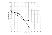
図1は、本発明者らの実験によるAl−2at%NiにN又はOを添加した場合の反射率の低下を示すグラフである。図1において、黒丸がOを添加した場合を示し、黒四角がNを添加した場合を示している。図1から明らかなように、Al−2at%NiにN又はOを添加した場合、添加量が増加するにつれて反射率は低下していく。しかし、Nを添加した場合に比べ、Oを添加した場合は反射率の低下を大きく抑制できることが分かった。 FIG. 1 is a graph showing a decrease in reflectance when N or O is added to Al-2 at% Ni according to experiments by the present inventors. In FIG. 1, the black circle shows the case where O is added, and the black square shows the case where N is added. As is apparent from FIG. 1, when N or O is added to Al-2 at% Ni, the reflectance decreases as the addition amount increases. However, it has been found that when O is added, a decrease in reflectance can be greatly suppressed as compared with the case where N is added.
さらに、図2は、AlNiにN又はOを添加した場合の比抵抗値の変化を表すグラフである。図2において、黒丸がOを添加した場合を示し、黒四角がNを添加した場合を示している。図2を見ると明らかなように、Nを添加した場合には、添加量が増加するにつれて比抵抗値は単調に増加していく。これに対し、Oを添加した場合には、添加量を増加しても比抵抗値が低下する領域があることが判った。本発明は、以上から得られた知見をもとになされたものである。 Further, FIG. 2 is a graph showing a change in specific resistance value when N or O is added to AlNi. In FIG. 2, the black circle shows the case where O is added, and the black square shows the case where N is added. As is apparent from FIG. 2, when N is added, the specific resistance value increases monotonously as the addition amount increases. On the other hand, when O was added, it was found that there was a region where the specific resistance value decreased even when the addition amount was increased. The present invention has been made based on the knowledge obtained from the above.
以下、本発明を適用可能な実施の形態について説明する。以下の説明は、本発明の実施形態を説明するものであり、本発明が以下の実施形態に限定されるものではない。説明の明確化のため、以下の記載及び図面は、適宜、省略及び簡略化がなされている。 Embodiments to which the present invention can be applied will be described below. The following description is to describe the embodiment of the present invention, and the present invention is not limited to the following embodiment. For clarity of explanation, the following description and drawings are omitted and simplified as appropriate.
実施の形態1.
本発明の実施の形態1に係る有機電界発光型表示装置について、図3を参照して説明する。図3は、本実施の形態に係る有機電界発光型表示装置の構成を示す断面図である。なお、図3においては、説明のため有機電界発光型表示装置構成するTFT基板とその上部に形成されている有機EL素子を含む画素部について図示している。図3に示すように、本実施の形態に係る有機電界発光型表示装置100は、絶縁性基板1、SiN層2、SiO2層3、ポリシリコン膜4、ゲート絶縁膜5、ゲート電極6、第1層間絶縁膜7、ソース電極10、ドレイン電極11、第2層間絶縁膜12、平坦化膜13、アノード15、分離膜16、電界発光層17、カソード18、封止層19、対向基板20を有している。
An organic electroluminescent display device according to
絶縁性基板1は、ガラス基板や石英基板等の透光性を有する基板である。絶縁性基板1上には、透光性絶縁膜であるSiN層2、SiO2層3が順次積層して形成されている。SiN層2、SiO2層3は、絶縁性基板1から流出する不純物から後述するTFTを保護するバッファ層としての役割を果たす。
The insulating
SiO2層3上には、半導体膜であるポリシリコン膜4が設けられる。ポリシリコン膜4は、SiO2層3上に島状に形成されている。ポリシリコン膜4は、ソース領域4a、ドレイン領域4b、チャネル領域4cとなる領域を含む。SiO2層3、ポリシリコン膜4を覆うようにして、ゲート絶縁膜5が形成されている。ゲート絶縁膜5上には、ゲート電極6が形成されている。
A
ゲート電極6の上には、SiO2等からなる第1層間絶縁膜7が形成されている。第1層間絶縁膜7及びゲート絶縁膜5には、これらの膜を貫通して設けられたコンタクトホール8、9が設けられている。コンタクトホール8は、下層に形成されたソース領域4aを露出するように開口されている。コンタクトホール9は、下層に形成されたドレイン領域4bを露出するように開口されている。
A first
第1層間絶縁膜7上には、ソース電極10、ドレイン電極11が形成されている。ソース電極10は、第1層間絶縁膜7及びゲート絶縁膜5に形成されたコンタクトホール8を介して、ソース領域4aと接続されている。また、ドレイン電極11は、第1層間絶縁膜7及びゲート絶縁膜5に形成されたコンタクトホール9を介して、ドレイン領域4bと接続されている。ソース電極10、ドレイン電極11、第1層間絶縁膜7上には、SiNやSiO2等からなる第2層間絶縁膜12が設けられている。また、第2層間絶縁膜12の上には、表面を平坦化するため、有機樹脂からなる平坦化膜13が設けられている。
A
第2層間絶縁膜12、平坦化膜13には、下層のドレイン電極11を露出させるコンタクトホール14、開口部がそれぞれ形成されている。平坦化膜13上には、アノード15が設けられている。アノード15は、第2層間絶縁膜12、平坦化膜13にそれぞれ形成されたコンタクトホール14、開口部を介して、下層のドレイン電極11と接続されている。アノード15は、第1アノードであるAl合金膜15aと、その上層に形成された第2アノードであるアモルファスITO膜15bとを積層してなる。Al合金膜15aは、8族3d遷移金属の1種以上と酸素とを含み、導電性を有する。アモルファスITO膜15bは、金属の酸化物を主成分とする透光性導電酸化膜(透明導電膜)である。アノード15の構成については、後に詳述する。
The second
アノード15及び平坦化膜13の上には、分離膜16が設けられている。分離膜16は、隣接する画素間を分離するために、画素周囲に額縁のように土手状に形成されている。分離膜16には、アノード15を露出する開口部が設けられている。分離膜16の開口部には、アノード15に接触するように、有機EL材料からなる電界発光層17が設けられている。電界発光層17は、図4に示すように、ホール輸送層17a、有機EL層17b、電子輸送層17cの順に積層される3層構造からなる。なお、ホール輸送層17aとアノード15との間に挟まれるホール注入層(不図示)、あるいは電子輸送層17cの直上に形成される電子注入層(不図示)の、いずれか少なくとも1層を追加した公知の構造でもよい。その場合、電界発光層17は、4層あるいは5層構造で形成される。
A
分離膜16、電界発光層17上には、カソード18が設けられている。アノード15、電界発光層17、カソード18が積層されて、EL素子が形成される。有機電界発光型表示装置には、複数の有機EL素子がマトリクス状に形成されている。カソード18は、ITO等で形成されている。アノード15とカソード18との間の電位差により、電界発光層17に電流を流す。カソード18の上には、封止層19が設けられている。封止層19は、電界発光層17を水分や不純物から遮断するために設けられている。封止層19上には、絶縁性基板1と対向するように対向基板20が設けられている。
A
図3に示す有機電界発光型表示装置においては、ソース電極10から伝わる信号電圧がドレイン電極11を介してアノード15に印加される。アノード15とカソード18との電位差により電界発光層17に電流が流れることにより有機EL層が発光するため、表示に必要な光を得ることができる。
In the organic electroluminescent display device shown in FIG. 3, a signal voltage transmitted from the
本実施の形態においては、アノード15の第1アノードであるAl合金膜15aは、光反射率の高いAlに、少なくとも8族3d遷移金属の1種以上を不純物として含み、反応性スパッタにより酸素が添加されており、導電性を有するものである。アノード15は、Al合金膜15aの上層にアモルファスITO膜15bを積層した、少なくとも2層膜として形成されている。このため、Al合金膜15aと、アモルファスITO膜15bとの界面においては、例えばアルミナ等の電気的絶縁性の界面反応物が存在しないと同時に、酸化インジウムの還元による金属Inの析出物が発生しない。
In the present embodiment, the
さらに、Al合金膜15aにおける、8族3d遷移元素から選ばれる1種以上の元素からなる不純物の組成比を0.1at%以上15at%以下とし、酸素の組成比を0.1at%以上8at%以下とする。これにより、光反射率が高く、透明導電膜であるアモルファスITO膜15bの還元によるダークスポットが発生しないアノード15を得ることができる。そのため、有機EL素子から発生する光の反射率が高いうえに、電界発光層17へのホール注入効率を高めることができる。従って、発光効率が高く、明るい表示画像を表示することができる有機電界発光型表示装置を得ることが可能となる。
Further, in the
次に、本実施の形態に係る有機電界発光装置の製造方法について、図5、6を参照して説明する。図5、6は、本実施の形態に係る有機電界発光型表示装置の製造方法を説明するための製造工程断面図である。なお、説明を簡単にするため、図5、6においては、p型のトランジスタのみを示している。 Next, a method for manufacturing the organic electroluminescent device according to the present embodiment will be described with reference to FIGS. 5 and 6 are cross-sectional views illustrating a manufacturing process for explaining the method for manufacturing the organic electroluminescent display device according to the present embodiment. For ease of explanation, FIGS. 5 and 6 show only p-type transistors.
図5(A)に示すように、まず、プラズマCVD(Chemical Vapor Deposition)法を用いて、絶縁性基板1の主表面上に、SiN膜2、SiO2膜3、及びアモルファスシリコン膜40を順に形成する。
As shown in FIG. 5A, first, the
なお、アモルファスシリコン膜40を形成した後、アモルファスシリコン膜40に含まれるH(水素)濃度を低減するために熱処理を実施しても良い。この場合、後に続くレーザアニール工程において、アモルファスシリコン膜40中の水素突沸によるクラックが発生することを防止することができる。
Note that after the
その後、図5(B)に示すように、エキシマレーザ(Excimer laser)から波長308nmのレーザ光をアモルファスシリコン膜40に向けて照射する。この際、レーザ光は、所定の光学系を通過して線状のビームプロファイルに変換された後、アモルファスシリコン膜40に向けて照射される。このレーザアニール工程によって、アモルファスシリコン膜40を多結晶化し、ポリシリコン膜4が形成される。
Thereafter, as shown in FIG. 5B, the
なお、本実施の形態では、アモルファスシリコン膜40を多結晶化する手段としてパルス型のエキシマレーザを用いたが、これに限定されるものではない。例えば、YAGレーザやCWレーザ(Continuous-wave laser)を用いてもよい。また、熱アニールを実施して、アモルファスシリコン膜40を多結晶化することも可能である。熱アニールを実施する場合、Ni(ニッケル)などの触媒を使用すれば、より大きい粒径のポリシリコン膜4を得ることができる。
In this embodiment, a pulse-type excimer laser is used as means for polycrystallizing the
次に、ポリシリコン膜4の上に、所定の開口パターンを有する図示しないレジスト膜を形成する。このレジスト膜をマスクとして、ポリシリコン膜4をエッチングし、ポリシリコン膜4を所定の形状とする。その後、レジスト膜を除去する。
Next, a resist film (not shown) having a predetermined opening pattern is formed on the
次に、プラズマCVD法を用いて、ポリシリコン膜4を覆うゲート絶縁膜5を形成する。そして、スパッタリング法を用いて、ゲート絶縁膜5上にゲート電極6となる金属膜を形成する。この金属膜上に所定の開口パターンを有する図示しないレジスト膜を形成する。このレジスト膜をマスクとして、金属膜をエッチングし、ゲート電極6を形成する。その後レジスト膜を除去する。
Next, a
その後、イオンドーピング法を用いて、ポリシリコン膜4に所定のドーズ量でボロンを注入する。このとき、ゲート電極6がマスクとなり、ボロンがポリシリコン膜4の両端に形成される。これにより、ポリシリコン膜4にソース領域4a、ドレイン領域4bが形成される。また、ボロンが注入されなかった箇所は、チャネル領域4cとなる。
Thereafter, boron is implanted into the
次に、図5(C)に示すように、ゲート絶縁膜5上にゲート電極6を覆う第1層間絶縁膜7を形成する。そして、第1層間絶縁膜7上に所定の開口パターンを有する図示しないレジスト膜を形成する。このレジスト膜をマスクとして第1層間絶縁膜7及びゲート絶縁膜5にエッチングを行うことにより、ソース領域4a、ドレイン領域4bにそれぞれ到達するコンタクトホール8、9を形成する。その後、レジスト膜を除去する。
Next, as shown in FIG. 5C, a first
次に、図5(D)に示すように、第1層間絶縁膜7上に、所定の形状を有するソース電極10、ドレイン電極11を形成し、コンタクトホール8を介してソース電極10とソース領域4aとを接続し、コンタクトホール9を介してドレイン電極11とドレイン領域4bとを接続する。ソース電極10、ドレイン電極11を形成した後、水素プラズマ雰囲気中に30分間、晒した状態とする。この工程により、ポリシリコン膜4に存在する欠陥をH(水素)で終端することができ、信頼性が高く、性能の高いトランジスタを形成することができる。
Next, as shown in FIG. 5D, a
次に、プラズマCVD法を用いて、第1層間絶縁膜7上に、ソース電極10、ドレイン電極11を覆う第2層間絶縁膜12を形成する。この第2層間絶縁膜12上に、所定の開口パターンを有する図示しないレジスト膜を形成する。このレジスト膜をマスクとして第2層間絶縁膜12をエッチングし、ドレイン電極11に到達するコンタクトホール14を形成する。その後、レジスト膜を除去する。
Next, a second
次に、図5(E)に示すように、第2層間絶縁膜12上に、コンタクトホール14の一部又は全部と重なるようにドレイン電極11に到達する開口部を有する平坦化膜13を形成する。平坦化膜13としては、有機樹脂膜、例えば、透光性のアクリル系観光樹脂膜であるJSR社製の製品名PC335を用いることができる。有機樹脂膜を約2μmの膜厚となるようにスピンコート法を用いて塗布形成し、フォトリソグラフィ法を用いてドレイン電極11に到達する開口部を形成する。その後、平坦化膜13をキュアするために、220℃のアニールを施す。これにより、所定の開口部を有する平坦化膜13が形成される。このように平坦化膜13を形成することにより、ゲート電極6やソース電極10、ドレイン電極11などの表面凹凸を被覆し、アレイ表面を平坦にすることができる。
Next, as shown in FIG. 5E, a
次に、平坦化膜13の上に、アノード15を形成する。具体的には、まず、アノード15の第1アノードとして、Al合金膜15aを形成する。
Next, the
本実施例では、アルミニウム(Al)にニッケル(Ni)を添加したターゲットを用い、アルゴン(Ar)に酸素(O)を不純物として混合した成膜ガスを用い、反応性スパッタリング法により、アルミニウムにニッケルを不純物として2at%、酸素を2at%添加した導電性を有するAl合金膜15aを50nmの厚さで成膜した。続いて、Al合金膜15aの上に、アノード15の第2アノードとして、透光性導電酸化膜であるアモルファスITO膜15bを20nmの厚さで成膜した。
In this embodiment, a target in which nickel (Ni) is added to aluminum (Al) is used, and a film forming gas in which oxygen (O) is mixed as an impurity in argon (Ar) is used. An
その後、写真製版工程により、アノード15上に所定の開口パターンを有するレジスト膜を形成する。そのレジスト膜をマスクとして、アノード15をエッチングする。まずシュウ酸を含む溶液を用い、続いて燐酸+硝酸+酢酸を含む溶液を用いて、順次アモルファスITO膜15b、酸素を含み導電性を有するAl合金膜15aをエッチングする。その後、レジスト膜を除去する。これにより、所望のパターンのAl合金膜15a、アモルファスITO膜15bの2層構造のアノード15が形成される。
Thereafter, a resist film having a predetermined opening pattern is formed on the
なお、本実施の形態においては、Alに不純物としてNiを添加したが、これに限定されるものではない。例えば、他の8族3d遷移金属であるFe、Coのいずれかを1種以上添加していれば良い。Alに8族3d遷移金属を1種以上添加することにより、上層に積層される透光性導電酸化膜との界面に絶縁性酸化物反応層が形成されるのを抑制することができ、ホール注入効率の低下を防止することができる。
In the present embodiment, Ni is added as an impurity to Al. However, the present invention is not limited to this. For example, at least one of Fe and Co, which are
図7に、金属膜と透光性導電酸化膜とのコンタクト抵抗値における、金属膜の材質依存性の結果を示す。図7から、AlにNiが添加されているAl合金膜にITO膜を積層した本実施例のコンタクト抵抗は、Niを添加していないAl膜とITO膜とを積層した従来例のコンタクト抵抗と比較すると、大幅に低減されていることがわかる。また、本実施例のコンタクト抵抗値は、比較例1、比較例2で示される、高融点金属であるMoやCrとITO膜を積層した場合のコンタクト抵抗値とほぼ同程度である。 FIG. 7 shows the result of the material dependence of the metal film on the contact resistance value between the metal film and the translucent conductive oxide film. From FIG. 7, the contact resistance of this example in which an ITO film is laminated on an Al alloy film in which Ni is added to Al is the contact resistance of a conventional example in which an Al film not added with Ni and an ITO film are laminated. When compared, it can be seen that it is greatly reduced. Further, the contact resistance value of this example is approximately the same as the contact resistance value obtained by laminating an ITO film with Mo or Cr, which is a refractory metal, shown in Comparative Examples 1 and 2.
このように、AlにNiを0.1at%以上添加することにより、Al合金膜と透光性導電酸化膜であるITO膜との間に形成される絶縁性酸化物反応層の生成を抑制することができる。これにより、良好な電気的コンタクト特性を得ることができる。 Thus, by adding 0.1 at% or more of Ni to Al, the generation of an insulating oxide reaction layer formed between the Al alloy film and the ITO film that is a light-transmitting conductive oxide film is suppressed. be able to. Thereby, favorable electrical contact characteristics can be obtained.
図8に、波長550nmにおけるAl合金膜の光反射率のNi組成依存性を示す。図8に示すように、Niの添加量が増加するにつれて、Al合金膜の反射率が低下することが分かる。Niの添加量を15at%以下とした場合には、Al合金膜の光反射率を比較例1のCrや、比較例2のMoの光反射率と同等以上にすることができる。これにより、電界発光層17からの光をAl合金膜で反射させ、表示光として寄与させることができる。従って、Al合金膜15aの、Alに添加するNiの組成比は、0.1at%以上15at%以下であることが好ましい。
FIG. 8 shows the Ni composition dependence of the light reflectance of the Al alloy film at a wavelength of 550 nm. As shown in FIG. 8, it can be seen that the reflectance of the Al alloy film decreases as the amount of Ni added increases. When the addition amount of Ni is 15 at% or less, the light reflectance of the Al alloy film can be made equal to or higher than the light reflectance of Cr of Comparative Example 1 or Mo of Comparative Example 2. Thereby, the light from the
また、本実施の形態では、Al合金膜15aとして、Niのほかにさらに不純物としてOを2at%添加したAl合金膜を用いたが、これに限定されない。Oの添加量は、0.1at%以上8at%以下にすることが望ましい。Oを0.1at%以上添加することにより、透明導電膜であるアモルファスITO膜15bの、Niによる還元を抑制することができる。このため、ダークスポットによる表示不良を防ぐことができる。
In the present embodiment, an Al alloy film to which 2 at% O is added as an impurity in addition to Ni is used as the
図1に、波長550nmにおけるAl合金膜の光反射率のO組成依存性を示す。図1に示すように、Oの添加量が増加するにつれて、Al合金膜の反射率が低下することが分かる。Oの添加量を8at%以下とした場合には、Al合金膜の光反射率をNを添加した場合の光反射率と同等以上にすることができる。これにより、電界発光層17からの光をAl合金膜で反射させ、表示光として寄与させることができる。従って、Al合金膜15aとしては、Alに添加するOの組成比は、0.1at%以上8at%以下であることが好ましい。
FIG. 1 shows the O composition dependence of the light reflectance of an Al alloy film at a wavelength of 550 nm. As shown in FIG. 1, it can be seen that the reflectance of the Al alloy film decreases as the amount of O added increases. When the addition amount of O is 8 at% or less, the light reflectance of the Al alloy film can be made equal to or higher than the light reflectance when N is added. Thereby, the light from the
さらに、Al合金膜15aに、希土類元素であるY、La、Ce、Pr、Nd、Sm、Gd、Tb、Dy、Ho、Erの1種以上をさらに添加することが望ましい。これらの不純物を添加することにより、Al合金膜15aの耐熱性を向上することができ、ヒロックを初めとする表面凹凸の発生を抑制することができる。このため、表面凹凸によるカソードとの電気的ショートを防止することができるため、所謂ダークスポットなどの表示不良の発生を抑制することができ、表示品位を向上させることができる。また、Al合金膜15aに添加する希土類元素であるY、La、Ce、Pr、Nd、Sm、Gd、Tb、Dy、Ho、Erの1種以上の元素の組成比率は、0.1at%以上15at%未満とし、前記8族3d遷移金属と合わせた組成比率の合計が15at%以下であることが好ましい。
Furthermore, it is desirable to further add one or more of rare earth elements Y, La, Ce, Pr, Nd, Sm, Gd, Tb, Dy, Ho, and Er to the
本実施の形態においては、Al合金膜15aの膜厚を50nmとしたが、10nm以上200nm以下であれば良い。図9に、波長550nmにおけるAl合金膜の光反射率と光透過率に対するAlの膜厚依存性を示す。図9から分かるように、Al合金膜の膜厚が10nm以上の場合、光透過率を十分低減でき、Al合金膜の光反射率を比較例1、2で示されたCrやMoと同等以上にすることができる。これにより、電界発光層17からの光をAl合金膜で反射させ、表示光として寄与させることができる。また、Al合金膜の膜厚が厚くなると、グレインサイズが大きくなり表面凹凸が粗くなる。このため、有機電界発光型表示装置のアノードとして用いる場合には、電界発光層17による被覆不良を引き起こし、カソード18とのショートモード故障等の要因となる。従って、アノード15の表面平滑性の指針としては、平均粗さRaが、1.0nm以下とすることが好ましい。この点を考慮すると、Al合金膜15aの膜厚は、200nm以下とすることが好ましい。
In the present embodiment, the thickness of the
また、アモルファスITO膜15bの膜厚を20nmとしたが、これに限らず、3.5nm以上の膜厚であればよい。3.5nmの膜厚であれば、層上に成長した均一な膜を形成することが可能であり、膜欠損による表示不良を防止できるという効果がある。
Moreover, although the film thickness of the
アモルファスITO膜15bは、ホール注入効率を高めるという作用のほかに、電界発光層17からの光が、アノード15のAl合金膜15aの表面で反射した場合の、光学経路要素のひとつとして作用することになる。従って、発光層である有機EL層17bからの光のうち、直接カソード18側へ放射される成分と、アノード15のAl合金膜15aで反射されてカソード18側へ放射される成分との干渉効果を考慮して、高い発光効率が得られるように、アモルファスITO膜15bの膜厚を設定することが好ましい。さらに、後述するように、電界発光層17における有機EL層17bの下層にホール輸送層17a等の膜が形成される場合には、これらの膜と、アモルファスITO膜15bとの積層構造による光学経路に基づいて、これらの層の厚みをそれぞれ設定することが好ましい。
The
以上のような、好ましい膜厚で成膜された透光性導電膜であるアモルファスITO膜15b、酸素を含んだ導電性を有するAl合金膜15aとの積層膜を、上述したように、写真製版工程により形成した所定のパターンを有するレジスト膜をマスクとして、エッチングする。まずシュウ酸を含む溶液を用い、続いて燐酸+硝酸+酢酸を含む溶液を用いて、順次エッチングすることより、アノード15を所望のパターンに加工した。燐酸+硝酸+酢酸を含む溶液を用いたエッチングにおいては、アモルファスITO膜15bは、Al合金膜15aよりもエッチング速度が遅い。このため、アノード15のパターンの断面は、Al合金膜15aの下層部のほうが狭く、アモルファスITO膜15bの上層のほうが広い庇形状となる。すなわち、アモルファスITO膜15bのパターンは、下層のAl合金膜15aのパターンから庇の分だけ飛び出している。つまり、アモルファスITO膜15bのパターンは、Al合金膜15aのパターンを内包した形となる。
As described above, the laminated film of the
このような庇形状を残したまま、図6(F)に示すように、アノード15の上に、分離膜16を形成すると、アノード15の庇の下部に空洞が形成されるため、そこに内包された水分や気泡等の不純物が、電界発光層17の劣化を引き起こす可能性がある。従って、レジスト膜を除去する前に、さらにシュウ酸を含む溶液でエッチングを追加しても良い。シュウ酸は、アモルファスITO膜15bをエッチングするが、酸素を含んだ導電性を有するAl合金膜15aをエッチングしないという選択性を有する。このような処理をすることにより、アノード15のパターンのエッジ部において、通常形成されるアモルファスITO膜15bの庇形状が改善され、略直線状又は図5(E)に示すように、順階段状に形成することができる。このため、この後に形成する分離膜16の被覆性を向上させることができ、電界発光層17の劣化を引き起こすおそれのある不純物の内包も防止できる。
When the
本実施の形態においては、透光性導電酸化膜としてアモルファスITO膜15bを用いたが、これに限らず、酸化インジウム(In2O3)、酸化スズ(SnO2)酸化亜鉛(ZnO)及びこれら酸化物を混合した材料であれば良い。これらは、燐酸+硝酸+酢酸でのエッチングが可能であるため、Al合金膜15aとの一括エッチングが可能であり、プロセスの簡略化ができるという効果を奏する。さらに、ZnO膜は、ITO膜やIn2O3膜、SnO2膜と比較して、Al合金膜15aとの界面反応性が低く、界面の凝集物の発生が少なくなる。この界面凝集物は、パネルの表示不良を引き起こすとともに、パネルの連続点灯によりさらにその生成に新構成を有するものである。従って、このような界面凝集物の生成を抑制できることは、パネルの高い表品質並びに高い信頼性を得るといった点で大きな利点がある。
In this embodiment, the
さらに、透光性導電酸化膜として酸化インジウム、酸化スズ、酸化亜鉛を混合した材料(ITZO)でもよい。ITZO膜の場合、ZnO膜の場合と同様に、Al合金膜15aとの界面反応性が低く、界面の凝集物の生成の抑制効果が大きい、さらに、ITZO膜の場合、アモルファスITO膜と同様に、熱処理によって結晶化するため、化学的安定性が向上するという効果も奏する。
Further, a material (ITZO) in which indium oxide, tin oxide, and zinc oxide are mixed may be used as the light-transmitting conductive oxide film. In the case of the ITZO film, as in the case of the ZnO film, the interface reactivity with the
次に、図6(F)に示すように、図3で示した電界発光層17を各画素部に分離して形成するための領域を確保するために、平坦化膜13及びアノード15の上に、ポリイミド等からなる有機樹脂膜を塗布形成し、写真製版工程により、分離膜16を形成する。分離膜16は、それぞれの画素領域を取り囲むように、額縁形状となるように設けられ、隣接する画素(不図示)間を分離するような土手状の凸部として形成される。分離膜16を形成する有機樹脂膜は、有機EL層17bの特性や信頼性に悪影響を及ぼす吸着水分の少ないポリイミド系の材料を用いることが望ましい。本実施の形態では、東レ社製の製品名DL100を約2μmの膜厚で塗布し、写真製版工程により額縁形状の分離膜16を形成した。
Next, as shown in FIG. 6F, in order to secure a region for forming the
次に、図6(G)に示すように、蒸着等の方法を用いて、電界発光層17となる有機材料を画素領域に形成する。本実施の形態では、電界発光層17として、図4に示すように、ホール輸送層17a、有機EL層17b、電子輸送層17cをこの順に積層して形成した。ホール輸送層17aとしては、公知のトリアリールアミン類、芳香族ヒドラゾン類、芳香族置換ピラゾリン類、スチルベン類等の有機系材料から幅広く選択することができる。例えば、N,N−ジフェニル−N,N−ビス(3−メチルフェニル)−1,1'−ジフェニル−4,4'ジアミン(TPD)等を1〜200nmの膜厚で形成する。
Next, as illustrated in FIG. 6G, an organic material to be the
有機EL層17bとしては、公知のジシアノメチレンピラン誘導体(赤色発光)、クマリン系(緑色発光)、キナクリドン系(緑色発光)、テトラフェニルブタジエン系(青色発光)、ジスチリルベンゼン系(青色発光)等の材料を1〜200nmの厚さで形成する。電子輸送層17cとしては公知のオキサジアゾール誘導体、トリアゾール誘導体、クマリン誘導体等から選ばれる材料を0.1〜200nmの膜厚で形成する。
Examples of the
上記の実施の形態では、電界発光層17をホール輸送層17a、有機EL層17b、電子輸送層17cを順次積層した構成としたが、これに限定されるものではない。電界発光層17の発光効率を上げるために、ホール輸送層17aとアノード15との間に、さらにホール注入層を設けてもよく、また電子輸送層17cと後述するカソード18との間に電子注入層を設ける公知の構成としてもよい。
In the above embodiment, the
次に、図6(G)に示すように、カソード18として、透明導電膜であるITO膜をスパッタリング法を用いて、100nmの厚さに形成する。カソード18は、画素領域において、下層の電界発光層17に接続される。また、カソード18は、図示しないコンタクトホールを介して、下層の陰極接地用電極(不図示)を接続される。カソード18は、膜面が高い平坦性を有することが好ましい。従って、膜組織に結晶粒界がない、アモルファスITO膜を形成することが好ましい。アモルファスITO膜は、例えば、ArガスにH2Oガスを混合させたガス中でのスパッタリングにより形成することができる。また、酸化インジウムと酸化亜鉛を混合させたIZO膜、あるいは、ITO膜に酸化亜鉛を混合させたITZO膜を用いることも可能である。
Next, as shown in FIG. 6G, an ITO film, which is a transparent conductive film, is formed as the
最後に、図6(H)に示すように、水分や不純物による電界発光層17の発光特性の劣化を防止するため、電界発光層17が形成されている画素領域全体を封止層19で覆い、その上に、対向基板20を配置する。これにより、本実施の形態に係る有機電界発光型表示装置が完成する。
Finally, as shown in FIG. 6H, the entire pixel region where the
なお、上記の実施の形態においては、画素を駆動するスイッチング素子となるTFTの半導体膜として、ポリシリコン膜4を用いたが、これに限らず、アモルファスシリコン膜を用いてもよい。また、TFTの構造も、本実施の形態1で示したようなトップゲート型に限らず、例えば、ボトムゲート逆スタッガード型等の構造としてもよい。また、本実施の形態1においては、TFTを1個しか図示しなかったが、画素ごとにTFTが複数個あってもよい。
In the above embodiment, the
実施の形態1では、アノード15の第1アノードであるAl合金膜15aを、アルミニウムにニッケルを添加したターゲットを用い、アルゴンに酸素を不純物として混合した成膜ガスを用いた反応性スパッタリング法を用いて形成したが、これに限定されない。例えば、Alに8族3d遷移金属と酸素を添加したターゲットを用いて、Arを成膜ガスとして用いたスパッタリング法により形成しても、同様の効果を得ることができる。
In the first embodiment, the
実施の形態2.
本発明の実施の形態2に係る有機電界発光型表示装置について、図10を参照して説明する。図10は、本実施の形態に係る有機電界発光型表示装置の構成を示す断面図である。本実施の形態において、実施の形態1と異なる点は、アノード21を第1Al合金膜21a、第2Al合金膜21b、アモルファスITO膜21cの3層構造とした点である。なお、図10において、図3と同一の構成要素には同一の符号を付し説明を省略する。
An organic electroluminescent display device according to the second embodiment of the present invention will be described with reference to FIG. FIG. 10 is a cross-sectional view showing the configuration of the organic electroluminescent display device according to this embodiment. The present embodiment is different from the first embodiment in that the
図10に示すように、本実施の形態では、アノード21は、第1アノードである第1Al合金膜21aと、その上層に形成された第2アノードである第2Al合金膜21bと、さらに上層に形成された第3アノードであるアモルファスITO膜21cとを積層した、少なくとも3層膜として形成されている。
As shown in FIG. 10, in this embodiment, the
第1Al合金膜21aは、光反射率の高いAlに、少なくとも8族3d遷移元素から選ばれる1種以上の元素を不純物として含む。また、第2Al合金膜21bは、Alに少なくとも8族3d遷移金属の1種以上を不純物として含み、反応性スパッタにより酸素が添加されており、導電性を有するものである。このため、第2Al合金膜21bと、アモルファスITO膜21cとの界面においては、例えばアルミナ等の電気的絶縁性の界面反応物が存在しない。
The first
さらに、第1Al合金膜21aにおける、8族3d遷移元素から選ばれる1種以上の元素からなる不純物の組成比を、0.1at%以上15at%以下とする。また、第2Al合金膜21bにおける、8族3d遷移元素から選ばれる1種以上の元素からなる不純物の組成比を0.1at%以上15at%以下とし、酸素の組成比を0.1at%以上8at%以下とする。これにより、実施の形態1で説明したように、光反射率が高く、アモルファスITO膜21cの還元によるダークスポットが発生しない。
Further, the composition ratio of the impurity composed of one or more elements selected from
このようなアノード21の製造方法としては、まず、アノード21の第1アノードとして、第1Al合金膜21aを形成する。本実施例では、アルミニウム(Al)にニッケル(Ni)を添加したターゲットを用い、アルゴン(Ar)を成膜ガスとして用いたスパッタリング法により、アルミニウムにニッケルを不純物として2at%添加した第1Al合金膜21aを50nmの厚さで成膜した。
As a method for manufacturing such an
次に、第1Al合金膜21aの上に、アノード21の第2アノードとして、第2Al合金膜21bを形成する。本実施例では、アルミニウム(Al)にニッケル(Ni)を添加したターゲットを用い、アルゴン(Ar)に酸素(O)を不純物として混合した成膜ガスを用い、反応性スパッタリング法により、アルミニウムにニッケルを不純物として2at%、酸素を2at%添加した導電性を有する第2Al合金膜21bを10nmの厚さで成膜した。続いて、第2Al合金膜21bの上に、アノード21の第3アノードとして、透光性導電酸化膜であるアモルファスITO膜21cを20nmの厚さで成膜した。
Next, a second Al alloy film 21b is formed as a second anode of the
その後、写真製版工程により、アノード21上に所定の開口パターンを有するレジスト膜を形成する。そのレジスト膜をマスクとして、アノード21をエッチングし、所望のパターンの第1Al合金膜21a、第2Al合金膜21b、アモルファスITO膜21cの3層構造のアノード21が形成される。
Thereafter, a resist film having a predetermined opening pattern is formed on the
実施の形態1では、アノード15の第1アノードをAl合金膜15aの単層構造としたが、実施の形態2のように、Alに少なくとも8族3d遷移金属の1種以上を不純物として含み、反応性スパッタにより酸素が添加されており、導電性を有する第2Al合金膜21bを上層とした積層構造としても、同様の効果を得ることができる。
In the first embodiment, the first anode of the
なお、酸素を含む導電性を有する第2Al合金膜21bの膜厚を10nmとしたが、これに限らず、3.5nm以上200nm以下であればよい。3.5nm以上の膜厚であれば、透明導電膜であるアモルファスITO膜21cの、Niによる還元を抑制することができ、ダークスポットによる表示不良の発生を防ぐことができる。また、Al合金膜の膜厚が厚くなると、グレインサイズが大きくなり表面凹凸が粗くなる。このため、有機電界発光型表示装置のアノードとして用いる場合には、電界発光層17による被覆不良を引き起こし、カソード18とのショートモード故障等の要因となる。従って、アノード21の表面平滑性の指針としては、平均粗さRaが、1.0nm以下とすることが好ましい。この点を考慮すると、第2Al合金膜21bの膜厚は、200nm以下とすることが好ましい。
In addition, although the film thickness of the 2nd Al alloy film 21b which has the electroconductivity containing oxygen was 10 nm, not only this but 3.5 nm or more and 200 nm or less should just be sufficient. If the film thickness is 3.5 nm or more, reduction of the amorphous ITO film 21c, which is a transparent conductive film, by Ni can be suppressed, and display defects due to dark spots can be prevented. Further, when the thickness of the Al alloy film is increased, the grain size is increased and the surface irregularities are roughened. For this reason, when used as an anode of an organic electroluminescent display device, the
また、上記の実施の形態では、第2Al合金膜21bを、アルミニウムにニッケルを添加したターゲットを用い、アルゴンに酸素を不純物として混合した成膜ガスを用いた反応性スパッタリング法を用いて形成したが、これに限定されない。例えば、Alに8族3d遷移金属と酸素を添加したターゲットを用いて、Arを成膜ガスとして用いたスパッタリング法により形成しても、同様の効果を得ることができる。
In the above embodiment, the second Al alloy film 21b is formed using a reactive sputtering method using a target obtained by adding nickel to aluminum and using a deposition gas in which oxygen is mixed as an impurity with argon. However, the present invention is not limited to this. For example, the same effect can be obtained even when a target obtained by adding a
なお、その場合には、第1アノードである第1Al合金膜21a、第2アノードである第2Al合金膜21bのそれぞれにターゲットが必要となる。反応性スパッタを用いた場合には、第1アノードと第2アノードを同一のターゲットによる形成することができるため、生産性を向上させることができる。
In this case, a target is required for each of the first
1 絶縁性基板
2 SiN膜
3 SiO2膜
4 多結晶シリコン膜
4a ソース領域
4b ドレイン領域
4c チャネル領域
5 ゲート絶縁膜
6 ゲート電極
7 第1層間絶縁膜
8、9 コンタクトホール
10 ソース電極
11 ドレイン電極
12 第2層間絶縁膜
13 平坦化膜
14 コンタクトホール
15、21 アノード
15a Al合金膜
15b、21c アモルファスITO膜
16 分離膜
17 電界発光層
17a ホール輸送層
17b 有機EL層
17c 電子輸送層
18 カソード
19 封止層
20 対向基板
21a 第1Al合金膜
21b 第2Al合金膜
40 アモルファスシリコン膜
DESCRIPTION OF
Claims (14)
前記薄膜トランジスタに接続され、少なくともアノード、電界発光層、カソードがこの順に積層されて形成された有機EL素子とを備え、
前記アノードは、
アルミニウムにNi、Fe、Coから選ばれる1種以上の不純物と酸素とを含み、導電性を有するAl合金膜と、
前記Al合金膜の上に形成された透明導電膜と、
を有し、
前記Al合金膜は、酸素が含まれる混合ガス中において形成されるか、又は、酸素が含まれるスパッタリングターゲットを用いて形成される有機電界発光型表示装置。 A thin film transistor formed on a substrate;
An organic EL element connected to the thin film transistor and formed by laminating at least an anode, an electroluminescent layer, and a cathode in this order;
The anode is
Al alloy film having conductivity and containing at least one impurity selected from Ni, Fe, Co and oxygen in aluminum;
A transparent conductive film formed on the Al alloy film;
Have
The Al alloy film may be formed in a mixed gas containing oxygen, or may be formed using a sputtering target containing oxygen .
前記透明導電膜は、金属の酸化物を主成分とするものであることを特徴とする請求項1に記載の有機電界発光型表示装置。 The composition ratio of the impurities added to the Al alloy film is 0.1 at% or more and 15 at% or less,
The organic electroluminescent display device according to claim 1, wherein the transparent conductive film contains a metal oxide as a main component.
前記アノードの形成工程は、
アルミニウムにNi、Fe、Coから選ばれる1種以上の不純物と酸素とを含み、導電性を有するAl合金膜を形成する工程と、
前記Al合金膜の上に透明導電膜を形成する工程と、
を含み、
前記Al合金膜を、アルゴンガスに酸素を混合した混合ガスを用いたスパッタリング方により形成するか、又は、アルミニウムに前記不純物と酸素とを含むAl合金スパッタリングターゲットを用いたスパッタリング法で形成することを特徴とする有機電界発光型表示装置の製造方法。 A method of manufacturing an organic electroluminescent display device comprising: a thin film transistor formed on a substrate; and an organic EL element connected to the thin film transistor and formed by laminating at least an anode, an electroluminescent layer, and a cathode in this order. ,
The anode forming step includes:
A step of forming an Al alloy film having conductivity, including at least one impurity selected from Ni, Fe, Co and oxygen in aluminum; and
Forming a transparent conductive film on the Al alloy film;
Only including,
The Al alloy film is formed by a sputtering method using a mixed gas in which oxygen is mixed with argon gas, or formed by a sputtering method using an Al alloy sputtering target containing the impurity and oxygen in aluminum. A method for manufacturing an organic electroluminescent display device.
前記透明導電膜を、金属の酸化物を主成分とするもので形成することを特徴とする請求項7に記載の有機電界発光型表示装置の製造方法。 The Al alloy film is formed by a sputtering method using an Al alloy sputtering target in which the impurities are added to aluminum at a composition ratio of 0.1 at% or more and 15 at% or less,
8. The method of manufacturing an organic electroluminescent display device according to claim 7 , wherein the transparent conductive film is formed of a metal oxide as a main component.
Priority Applications (2)
| Application Number | Priority Date | Filing Date | Title |
|---|---|---|---|
| JP2008020501A JP5007246B2 (en) | 2008-01-31 | 2008-01-31 | Organic electroluminescent display device and manufacturing method thereof |
| US12/358,744 US8040054B2 (en) | 2008-01-31 | 2009-01-23 | Organic electroluminescence type display apparatus and method of manufacturing the same |
Applications Claiming Priority (1)
| Application Number | Priority Date | Filing Date | Title |
|---|---|---|---|
| JP2008020501A JP5007246B2 (en) | 2008-01-31 | 2008-01-31 | Organic electroluminescent display device and manufacturing method thereof |
Publications (2)
| Publication Number | Publication Date |
|---|---|
| JP2009181836A JP2009181836A (en) | 2009-08-13 |
| JP5007246B2 true JP5007246B2 (en) | 2012-08-22 |
Family
ID=40931002
Family Applications (1)
| Application Number | Title | Priority Date | Filing Date |
|---|---|---|---|
| JP2008020501A Active JP5007246B2 (en) | 2008-01-31 | 2008-01-31 | Organic electroluminescent display device and manufacturing method thereof |
Country Status (2)
| Country | Link |
|---|---|
| US (1) | US8040054B2 (en) |
| JP (1) | JP5007246B2 (en) |
Families Citing this family (12)
| Publication number | Priority date | Publication date | Assignee | Title |
|---|---|---|---|---|
| JP2007093686A (en) | 2005-09-27 | 2007-04-12 | Mitsubishi Electric Corp | Liquid crystal display device and manufacturing method thereof |
| CN102334385A (en) | 2009-09-14 | 2012-01-25 | 松下电器产业株式会社 | Display panel device and manufacturing method of display panel device |
| KR101782557B1 (en) * | 2010-10-25 | 2017-09-28 | 삼성디스플레이 주식회사 | Organic light emitting display device and manufacturing method of the same |
| KR102212457B1 (en) * | 2013-05-30 | 2021-02-04 | 엘지디스플레이 주식회사 | Organic light emitting display device and manufacturing method of the same |
| KR102520874B1 (en) * | 2015-05-29 | 2023-04-12 | 엘지디스플레이 주식회사 | Organic light emitting display device and method of manufacturing the same |
| JP2018032601A (en) * | 2016-08-26 | 2018-03-01 | 株式会社神戸製鋼所 | REFLECTION ELECTRODE AND Al ALLOY SPUTTERING TARGET |
| CN107342375B (en) * | 2017-08-21 | 2019-05-31 | 深圳市华星光电半导体显示技术有限公司 | The production method and flexible display panels of flexible display panels |
| CN107863458B (en) * | 2017-10-30 | 2019-11-15 | 武汉华星光电半导体显示技术有限公司 | The production method of the production method and OLED display of oled substrate |
| JP6926169B2 (en) | 2018-03-28 | 2021-08-25 | 堺ディスプレイプロダクト株式会社 | Organic EL display device and its manufacturing method |
| JP6603826B1 (en) | 2018-03-28 | 2019-11-06 | 堺ディスプレイプロダクト株式会社 | Organic EL display device and manufacturing method thereof |
| KR20220033650A (en) * | 2020-09-09 | 2022-03-17 | 삼성디스플레이 주식회사 | Reflective electrode and display device having the same |
| US11810907B2 (en) | 2021-01-27 | 2023-11-07 | Taiwan Semiconductor Manufacturing Company, Ltd. | Pixel structure for displays |
Family Cites Families (20)
| Publication number | Priority date | Publication date | Assignee | Title |
|---|---|---|---|---|
| US4720432A (en) | 1987-02-11 | 1988-01-19 | Eastman Kodak Company | Electroluminescent device with organic luminescent medium |
| JPH04253342A (en) | 1991-01-29 | 1992-09-09 | Oki Electric Ind Co Ltd | Thin film transistor array substrate |
| JP3219450B2 (en) * | 1992-01-24 | 2001-10-15 | 旭硝子株式会社 | Method for producing conductive film, low reflection conductive film and method for producing the same |
| JP2886014B2 (en) | 1992-12-24 | 1999-04-26 | キヤノン株式会社 | Solar cell specular reflection film, method of forming the same, solar cell and method of manufacturing the same |
| US6297519B1 (en) * | 1998-08-28 | 2001-10-02 | Fujitsu Limited | TFT substrate with low contact resistance and damage resistant terminals |
| JP3288637B2 (en) | 1998-08-28 | 2002-06-04 | 富士通株式会社 | ITO film connection structure, TFT substrate and method of manufacturing the same |
| AU3056301A (en) * | 2000-02-02 | 2001-08-14 | Mitsubishi Chemical Corporation | Organic electroluminescent element and method of manufacture thereof |
| US6559594B2 (en) * | 2000-02-03 | 2003-05-06 | Semiconductor Energy Laboratory Co., Ltd. | Light-emitting device |
| JP3967081B2 (en) | 2000-02-03 | 2007-08-29 | 株式会社半導体エネルギー研究所 | Light emitting device and manufacturing method thereof |
| JP3804858B2 (en) * | 2001-08-31 | 2006-08-02 | ソニー株式会社 | Organic electroluminescent device and manufacturing method thereof |
| JP2003288993A (en) | 2002-03-27 | 2003-10-10 | Tokai Rubber Ind Ltd | Transparent electrode for organic electroluminescent element and organic electroluminescent element using the same |
| KR100477746B1 (en) | 2002-06-22 | 2005-03-18 | 삼성에스디아이 주식회사 | Organic electroluminescence device employing multi-layered anode |
| JP3940385B2 (en) | 2002-12-19 | 2007-07-04 | 株式会社神戸製鋼所 | Display device and manufacturing method thereof |
| JP2004363556A (en) | 2003-05-13 | 2004-12-24 | Mitsui Mining & Smelting Co Ltd | Semiconductor device |
| JP4148182B2 (en) * | 2004-05-17 | 2008-09-10 | ソニー株式会社 | Display device |
| JP4541787B2 (en) * | 2004-07-06 | 2010-09-08 | 株式会社神戸製鋼所 | Display device |
| KR100647660B1 (en) * | 2004-11-19 | 2006-11-23 | 삼성에스디아이 주식회사 | A thin film transistor, and a flat panel display employing the same |
| JP2006236839A (en) * | 2005-02-25 | 2006-09-07 | Mitsubishi Electric Corp | Organic electroluminescent display device |
| US20060240280A1 (en) * | 2005-04-21 | 2006-10-26 | Eastman Kodak Company | OLED anode modification layer |
| JP2007123672A (en) * | 2005-10-31 | 2007-05-17 | Mitsubishi Electric Corp | Conductor structure, method for manufacturing the same, element substrate and method for manufacturing the same |
-
2008
- 2008-01-31 JP JP2008020501A patent/JP5007246B2/en active Active
-
2009
- 2009-01-23 US US12/358,744 patent/US8040054B2/en active Active
Also Published As
| Publication number | Publication date |
|---|---|
| US8040054B2 (en) | 2011-10-18 |
| JP2009181836A (en) | 2009-08-13 |
| US20090195151A1 (en) | 2009-08-06 |
Similar Documents
| Publication | Publication Date | Title |
|---|---|---|
| JP5007246B2 (en) | Organic electroluminescent display device and manufacturing method thereof | |
| KR100764673B1 (en) | Organic electroluminescence type display apparatus | |
| US7579767B2 (en) | Organic light emitting device having triple layered pixel electrode | |
| EP1606848B1 (en) | Light-emitting device, method of manufacturing the same, and display unit | |
| JP5348299B2 (en) | Light emitting display device and manufacturing method thereof | |
| US7687984B2 (en) | Organic light emitting display device and method for fabricating the same | |
| US8963134B2 (en) | Display panel and method for manufacturing the same | |
| JP4637831B2 (en) | ORGANIC ELECTROLUMINESCENCE ELEMENT, ITS MANUFACTURING METHOD, AND DISPLAY DEVICE | |
| JPWO2012073269A1 (en) | Organic EL panel, organic EL panel manufacturing method, organic light emitting device using organic EL panel, and organic display device using organic EL panel | |
| US9099677B2 (en) | Encapsulation structure for an organic light emitting display device, an organic light emitting display device, and methods of manufacturing an organic light emitting display device | |
| JP2006351844A (en) | Electro-optical display device and its manufacturing method | |
| KR100635065B1 (en) | Organic light emitting display device and the method for fabricating of the same | |
| JP4556768B2 (en) | Organic electroluminescent display | |
| KR102484903B1 (en) | Organic light emitting device and method of fabricating the same | |
| WO2012066592A1 (en) | Organic el element, display panel, and display device | |
| JP2005285395A (en) | Wiring structure, substrate for display device provided with it and display device | |
| WO2013187046A1 (en) | Thin film transistor | |
| JP4532892B2 (en) | Organic EL element and organic EL display device | |
| KR20220056844A (en) | Organic light emitting display device | |
| JP4463075B2 (en) | Transflective liquid crystal display device, method for producing transflective liquid crystal display device, TFT substrate, and method for producing TFT substrate | |
| JP2010199079A (en) | Organic el element and display device | |
| JP5117553B2 (en) | Manufacturing method of display device | |
| JP2008103253A (en) | Display and its manufacturing method |
Legal Events
| Date | Code | Title | Description |
|---|---|---|---|
| A621 | Written request for application examination |
Free format text: JAPANESE INTERMEDIATE CODE: A621 Effective date: 20101208 |
|
| A977 | Report on retrieval |
Free format text: JAPANESE INTERMEDIATE CODE: A971007 Effective date: 20120111 |
|
| A131 | Notification of reasons for refusal |
Free format text: JAPANESE INTERMEDIATE CODE: A131 Effective date: 20120131 |
|
| A521 | Request for written amendment filed |
Free format text: JAPANESE INTERMEDIATE CODE: A523 Effective date: 20120329 |
|
| TRDD | Decision of grant or rejection written | ||
| A01 | Written decision to grant a patent or to grant a registration (utility model) |
Free format text: JAPANESE INTERMEDIATE CODE: A01 Effective date: 20120508 |
|
| A01 | Written decision to grant a patent or to grant a registration (utility model) |
Free format text: JAPANESE INTERMEDIATE CODE: A01 |
|
| A61 | First payment of annual fees (during grant procedure) |
Free format text: JAPANESE INTERMEDIATE CODE: A61 Effective date: 20120528 |
|
| FPAY | Renewal fee payment (event date is renewal date of database) |
Free format text: PAYMENT UNTIL: 20150601 Year of fee payment: 3 |
|
| R151 | Written notification of patent or utility model registration |
Ref document number: 5007246 Country of ref document: JP Free format text: JAPANESE INTERMEDIATE CODE: R151 |
|
| FPAY | Renewal fee payment (event date is renewal date of database) |
Free format text: PAYMENT UNTIL: 20150601 Year of fee payment: 3 |
|
| R250 | Receipt of annual fees |
Free format text: JAPANESE INTERMEDIATE CODE: R250 |
|
| R250 | Receipt of annual fees |
Free format text: JAPANESE INTERMEDIATE CODE: R250 |
|
| R250 | Receipt of annual fees |
Free format text: JAPANESE INTERMEDIATE CODE: R250 |
|
| R250 | Receipt of annual fees |
Free format text: JAPANESE INTERMEDIATE CODE: R250 |
|
| R250 | Receipt of annual fees |
Free format text: JAPANESE INTERMEDIATE CODE: R250 |
|
| R250 | Receipt of annual fees |
Free format text: JAPANESE INTERMEDIATE CODE: R250 |
|
| R250 | Receipt of annual fees |
Free format text: JAPANESE INTERMEDIATE CODE: R250 |
|
| R250 | Receipt of annual fees |
Free format text: JAPANESE INTERMEDIATE CODE: R250 |