JP4132424B2 - Manufacturing method of liquid crystal optical element - Google Patents
Manufacturing method of liquid crystal optical element Download PDFInfo
- Publication number
- JP4132424B2 JP4132424B2 JP17522199A JP17522199A JP4132424B2 JP 4132424 B2 JP4132424 B2 JP 4132424B2 JP 17522199 A JP17522199 A JP 17522199A JP 17522199 A JP17522199 A JP 17522199A JP 4132424 B2 JP4132424 B2 JP 4132424B2
- Authority
- JP
- Japan
- Prior art keywords
- liquid crystal
- optical element
- substrate
- composition
- compound
- Prior art date
- Legal status (The legal status is an assumption and is not a legal conclusion. Google has not performed a legal analysis and makes no representation as to the accuracy of the status listed.)
- Expired - Fee Related
Links
Images
Landscapes
- Liquid Crystal (AREA)
- Liquid Crystal Substances (AREA)
Abstract
Description
【0001】
【発明の属する技術分野】
本発明は、電圧の印加・非印加により、素子の透過、散乱、反射状態を制御し、調光素子や表示素子、光学シャッタ等に用いる液晶光学素子に関する。
【0002】
【従来の技術】
液晶と透明な高分子とを複合して、高分子と液晶との間の屈折率差、または液晶内部(微小領域間)における屈折率差を利用した、透過−散乱型の動作モードを有する液晶光学素子が提案された。液晶/高分子複合体素子、液晶/樹脂複合体素子または分散型液晶素子などと呼ばれている。この液晶光学素子は原理的に偏光板を必要としないので、光の吸収損失が少なく、かつ高い散乱性能が得られるので光の利用効率が高い。
【0003】
この液晶光学素子は、その特性を生かして、調光窓、光シャッタ素子、レーザー装置および表示装置などに用いられている。電圧非印加で散乱状態、電圧印加で透明状態のものが商用化された。
【0004】
従来例1(US5188760)では、液晶と重合性の液晶を用いた素子が開示された。この従来例1は、電圧非印加時において素子内の液晶と重合された液晶とが同じ配向方向を有しているので、素子をどの方向から見ても透明状態を呈する。そして、電圧印加時には、素子内の液晶の配向が電界によって制御され、液晶分子の配列方向が微小領域においてさまざまに変化することにより、素子は散乱状態を呈する。
【0005】
また、カイラル剤を液晶に添加して初期配向にヘリカル構造を設けることによって、コントラスト比が向上する。この素子の特徴的構造は、「異方性ゲル」または「液晶ゲル」と呼ばれている。従来例1ではアクリロイル基を末端に持つメソゲンモノマーが使用された。
【0006】
また、従来例2(国際特許公開WO92/19695)にも同様の構成を持つ素子が開示された。従来例1と同様の動作モードを有しており、カイラルネマチック液晶中に微量の高分子を分散させ、電圧非印加時に透明状態、電圧印加時に散乱状態を得る。この素子はPSCT(ポリマー・スタビライズド・コレステリック・テクスチャー)と呼ばれている。この従来例2にもアクリロイル基を末端に持つメソゲンモノマーが用いられた。
【0007】
【発明が解決しようとする課題】
従来例1において、組成物全体が液晶相を示す状態で硬化物を硬化せしめて素子を形成することが示された。その製造方法では基板間に未硬化の組成物を挟持してから硬化を行う。
【0008】
このように、組成物を硬化することによって形成された素子において、硬化後における液晶/硬化物複合体の流動性は小さく、封止工程を組成物の挟持後に行うこともできる。生産性を向上するためには大型基板やフィルム基板を用いて素子を形成し、その後に基板を切断してから封止を行うことが望ましい。この際に素子と基板の接着力が低い場合は切断時に素子と基板の剥離が生じ、封止部分から素子内面にかけて不良部分が発生する問題点があった。
接着力を向上させる方法としては、基板間の距離を一定に保つために用いられるスペーサに基板との接着力を持たせる方法もあるが、スペーサの数を増やせば接触面積を大きくできる一方で光学特性に対する悪影響が起こるために、スペーサの数を増やすことには一定の限界がある。
【0009】
本発明は、これらの問題を解決するものである。さらに、形成後の液晶光学素子の光の透過率が高く、かつ基板面における光学特性の均一性が優れた素子を得ようとする。また、微小領域の配向を均一に形成して、高密度表示に適した素子を得ようとする。
【0010】
【課題を解決するための手段】
すなわち本発明は、少なくとも一方が透明な2枚の電極付き基板間に、液晶と硬化性化合物を含有する組成物を挟持し、組成物の一部または全体が液晶相を示す状態で前記硬化性化合物の硬化を行い、液晶/硬化物複合体を形成する液晶光学素子の製造方法において、基板と組成物との間に、前記硬化性化合物と反応し、かつ前記硬化性化合物の重合反応形式と同種の重合反応形式を有する有機金属化合物を含有する層を配置して硬化を行うことを特徴とする液晶光学素子の製造方法を提供する。
【0011】
また、組成物の一部または全体が液晶相を示すときに、前記層によって組成物に配向性を付与する上記の製造方法を提供する。
また、重合反応形式がラジカル重合である上記の製造方法を提供する。
また、前記硬化を行う前に、前記層の仮焼成と本焼成を行う上記の製造方法を提供する。
また、前記層に含有せしめる有機金属化合物は、前記層の全量に対して、3〜90重量%である上記の製造方法を提供する。
【0013】
上記の製造方法において、配向性とは、組成物を配向させる機能を呈するラビング法や偏光を用いた処理によって得られた液晶を配向させる機能である。実効的に、配向性を発現または向上させるものであればよい。
【0014】
【発明の実施の形態】
本発明では基板間に液晶と硬化性化合物を含有する組成物を挟持して、組成物の一部または全部が液晶相を示す状態で硬化を行うことによって液晶光学素子を形成する。硬化物と液晶の分量比などによって、種々の構造をとりうるが、電圧印加により発生した電界に対して、液晶のみが実質的に応答するように、液晶と硬化物が分離した構造をもつ。さらに、硬化後に液晶と硬化物の配向が一定であれば光学的な均一性が高まるので好ましい。
【0015】
本発明では基板間に液晶と硬化性化合物を含有する組成物を挟持して、組成物の一部または全部が液晶相を示す温度で、硬化性化合物を硬化せしめることによって液晶光学素子を形成する。その際に、基板と組成物との間に、通常は組成物と接する面に、組成物中の硬化性化合物と反応しうる化合物(以下、反応性化合物と呼ぶ)を含有する層を配置する。そして、前記硬化性化合物の硬化の際、前記硬化性化合物と反応性化合物との間に化学結合を生じることによって、接着力を高めるものである。以下、この化合物を含有する層を接着層と呼ぶ。
【0016】
本発明に用いられる液晶は変化させる光学特性の動作モードに応じて任意に選択できる。透過・散乱の動作モードの液晶光学素子を製造しようとする場合においてはネマチック液晶をそのまま用いる。ネマチック液晶にカイラル剤を混合したカイラルネマチック液晶(コレステリック液晶とも呼ばれる)を用いてもよい。反射・透過の動作モードやメモリ性を有する反射・散乱の動作モードの液晶光学素子を製造しようとする場合には、液晶光学素子によって反射させようとする波長に合わせてカイラル剤を混合し、液晶の屈折率とカイラルピッチを調整したカイラルネマチック液晶を用いる。応答速度が遅くなる傾向を示すが、スメクチック液晶やカイラルスメクチック液晶を用いることもできる。
【0017】
本発明に用いる硬化性化合物はどのような反応様式で硬化してもよい。反応様式はラジカル重合、カチオン重合、アニオン重合を代表とする連鎖重合、重付加を代表とする逐次重合のいずれも利用できる。液晶と反応性化合物を含有する組成物を準備して用いればよい。通常は、硬化性化合物を液晶に溶解する。ただし、硬化性化合物を液晶に溶解したときに、組成物の一部または全体が液晶相を示す温度が存在することが必須条件である。ここで、一部が液晶相を示すとはミクロに物質が分離した状態となり、液晶性を示していない微小な部位が存在することを意味する。
【0018】
しかし、素子全体を見た場合には、マクロに液晶相を示すものである。そして、そのような状態から形成された液晶光学素子を肉眼視した場合に、基板面全体にわたってほぼ一様な光学特性(透過・散乱)を示す程度のものであればよい。
【0019】
液晶と硬化性化合物の比率は任意であるが、硬化性化合物の体積分率があまり多すぎると液晶に溶解しなかったり、全体が液晶相を示す温度が存在しない場合がある。また、形成した液晶光学素子の動作・非動作時の光学特性の変化が小さくなる。また、硬化性化合物の分量が少なすぎると硬化物の安定性が失われ、機械的な外圧に対して弱くなったり、高温での信頼性が低下する。一般的には、液晶と硬化性化合物との全量に対する硬化性化合物の重量比は1〜50%が好ましく、10〜30%がより好ましい。
【0020】
反応性化合物の例としてはアクリロイル基やメタクリロイル基、アリル基、ビニル基、エポキシ基など有する化合物があげられる。実用的には硬化性化合物の硬化部位と同種の反応形式であることが好ましい。例えば、ラジカル重合によりアクリロイル基を有する硬化性化合物を硬化させる場合には反応性化合物もラジカル重合による反応性が高いアクリロイル基やメタクリロイル基を有する化合物が好適である。また、エポキシ基のような開環重合する官能基を有する硬化性化合物を硬化させる場合には、反応性化合物も開環重合を行う同種の基もしくは対となる官能基、すなわち水酸基やチオール基、アミノ基などを有する化合物や酸無水物を用いることが好適である。
【0021】
接着層に含有せしめる反応性化合物は、全量に対して、3〜90重量%が好ましく、10〜70重量%がより好ましい。反応性化合物の含有量が少なすぎる場合は接着性が弱く、多すぎる場合には、組成物中に含まれた硬化性化合物の硬化前に液晶が均一な配向を示していても、硬化後に液晶の配向に乱れを生じ、液晶光学素子として所望の光学特性を得ることが難しくなる。この点が従来技術のうちの、液晶相を示さない状態で硬化工程を行う従来技術の液晶光学素子と大きく異なる。
【0022】
本発明の液晶光学素子は硬化時に一部または全部が液晶相を有するようにして形成する。その際に組成物の配向が一定でなければ形成された液晶光学素子の光学的均一性が低下するため、接着層は組成物を配向させる効果を合わせもつことが好ましい。組成物の配向は水平配向または垂直配向のいずれでもよく、水平配向の場合、一対の基板の各配向軸のなす角度は任意の角度を採用できる。
【0023】
また、組成物の配向を水平配向とする場合には、接着層として有機高分子層を使用できる。組成物の配向を垂直配向とする場合には、接着層として有機高分子膜または有機金属化合物の薄膜を使用できる。接着層は一対の基板のうち片方に設置されていてもよいが、両方に設置されている方がより好ましい。
【0024】
この場合、有機高分子層としては、従来より液晶配向膜として用いられている高分子膜に反応性化合物を混合した層や、反応性部位を側鎖として有する高分子を含む層が用いられる。高分子の種類は水平配向・垂直配向の配向の種類に合わせて適切に選ぶ。また、接着層を形成した後、ラビングや偏光などを用いて配向能力をさらに付加できる。このような高分子の例としてはポリイミド、ポリビニルアルコール、光反応性を有する高分子などがあげられる。また、ポリアミック酸のようにそれらの前駆体であってもよい。
また、組成物の配向を垂直配向とする場合であって、ラビング法を用いないときには、機械的な膜の摩耗を考えなくてよいので、反応性化合物として有機金属化合物を用いることもできる。
【0025】
この有機金属化合物は基板や基板上の電極との接着性が良好で、硬化性化合物と反応しうるシランカップリング剤やチタネートカップリング剤を用いる。さらに組成物を垂直配向させるために、垂直配向性を有するシランカップリング剤やチタネートカップリング剤を混合したり、両者を化学結合させたりする。
【0026】
上記有機金属化合物として以下の化合物があげられる。3−アクリロキシプロピルトリメトキシシラン、3−アクリロキシプロピルトリクロロシラン、3−アクリロキシプロピルメチルジメトキシシラン、3−メタクリロキシプロピルトリメトキシシラン、3−アクリロキシプロピルトリプロポキシチタン、3−メタクリロキシプロピルトリブトキシチタン、3−グリシドキシプロピルトリメトキシシラン、3−アミノプロピルトリエトキシシランなどである。
【0027】
また、接着層に垂直配向性を誘起し、上記の反応性化合物と併用できる化合物としては、フルオロアルキルシランや長鎖アルキルシランが用いられる。フルオロアルキルシランとしてはヘプタデカフルオロデシルメチルジメトキシシラン、ヘプタデカフルオロデシルトリメトキシシラン、トリデカフルオロオクチルトリメトキシシランなどがあげられる。長鎖アルキルシランとしてはオクチルトリメトキシシラン、オクタデシルトリメトキシシラン、オクタデシルトリエトキシシランなどがあげられる。
【0028】
これら有機金属化合物は加水分解可能な基を有しており、通常「水−アルコール系」溶媒に溶解して加水分解し、基板に塗布した後加熱乾燥させることで基板上に薄膜を形成できる。なお、加水分解時に酢酸等でpH調整を行ってもよい。このようにして形成した接着層は、基板面に対して好ましい接着性を有している。
【0029】
液晶と未硬化の硬化性化合物の組成物は、混合後均質な溶液であることが好ましい。この組成物は、電極付き基板に挟持されるとき、液晶相でも等方相でもよい。組成物中の硬化性化合物を硬化させるときには、組成物の一部または全体が液晶相を示す温度に設定する。
【0030】
接着層を形成した後、ラビングや偏光などを用いてプレチルト角を調節することもできる。ラビング法などの付加的な配向処理を行わない場合には、機械的な膜の摩耗を考えなくてよい。そのため、ポリイミド等の有機高分子膜ではなく、有機金属化合物の薄膜を用いて電極と直接接着できる。
【0031】
本発明において、液晶光学素子の電極間隙は、スペーサ等で保持できる。スペーサのサイズとしては、2〜50μmが好ましく、さらに4〜30μmが好ましい。この電極間隙は小さすぎるとコントラスト比が低下し、大きすぎると駆動電圧が上昇する。
【0032】
電極を支持する基板は、ガラス基板でも樹脂基板でもよく、またガラス基板と樹脂基板の組み合わせでもよい。また、片方の基板にアルミニウムなどの金属や誘電体多層膜が設けられてもよい。
【0033】
フィルム基板の場合は、連続で供給される電極付き基板を2本のゴムロール等で挟み、その間に、スペーサを含有分散させた液晶と未硬化の硬化性化合物とを含有する組成物を供給し、挟み込み、連続で硬化させることができる。したがって、フィルム基板の製造法は生産性が高い。
【0034】
ガラス基板の場合は、電極面内に微量のスペーサを散布し、対向させた基板の4辺をエポキシ樹脂等のシール剤で封止セルとし、シールの切り欠きを2カ所以上設け、シールの切り欠きの一箇所を液晶と未硬化の硬化性化合物の組成物に浸し、他方の切り欠きよりセル内を吸引する。そして、セル内に組成物を満たし、硬化性化合物を硬化させ、動作可能な液晶光学素子を得る。また、通常の真空注入法を用いることもできる。
【0035】
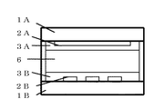
図1を参照して本発明によって形成された液晶光学素子の構成例を説明する。図1は、表側基板1A、表側電極2A、表側接着層3A、液晶/硬化物複合体6(液晶および硬化物)、裏側接着層3B、裏側電極2B、裏側基板1Bの配置状態を示す断面図である。表側電極2Aと裏側電極2Bは直交するように配置された線状の電極で電極間に電圧を印加する。この構成例では画素毎をオン・オフ制御することでドットマトリックス表示を行うことができる。後述する実施例1では全面べた電極として、面全体のオン・オフを行う液晶光学素子とした。例えば、調光窓などに用いることができる。
【0036】
液晶/硬化物複合体中における液晶の体積分率の多い場合には、セル化した基板の周辺部にシールを設ける。硬化物の体積分率が多い場合には、周辺シールなしで素子を製造することもできる。図1では、スペーサその他の部材の図示を省略している。
【0037】
【実施例】
(実施例1)
JALS−682−R6(JSR社製、垂直配向能を有するポリイミドを固形分濃度3.0%に希釈した液状物)を5g、反応性化合物としてトリメチロールプロパントリアクリレートを0.0375g、希釈溶媒としてACT−649(JSR社製)を1.2125g混合し、ITO透明電極付きソーダライムガラスに500rpmで2秒および2000rpmで20秒の条件でスピンコートした。コート後に、仮焼成60℃・1分、および本焼成120℃・60分の条件で焼成した。焼成後の膜厚は約70nmであった。
【0038】
さらに、負の誘電異方性を有するネマチック液晶(チッソ社製 AG−1016XX)85部、下記式1の未硬化の硬化性化合物12部、下記式2の未硬化の硬化性化合物3部、ベンゾインイソプロピルエーテル0.45部からなる組成物を調製した。本例では、組成物中に2種類の硬化性化合物を含有せしめ、接着層中の反応性化合物と同種の反応形式(アクリロイル基を有する化合物)をもつ組み合わせとなるように設定した。
【0039】
【化1】

この組成物を、微量の直径6μmの樹脂ビーズを介して、上記のように準備した2枚の透明電極付きガラス基板の間に挟持した。組成物全体が液晶性を示すように温度を調整した。そして、組成物が液晶性を示す状態において、紫外線照射により組成物中の硬化性化合物を硬化せしめて液晶/硬化物複合体を形成し、電気的に光学特性を制御できる液晶光学素子を得た。紫外線照射条件は37℃に保持した状態で組成物全体は液晶相を示しており、主波長が約365nmのHgXeランプにより、一対の基板の上側より約3mW/cm2、下側より同じく約3mW/cm2の紫外線を30分間照射した。
【0041】
硬化前と同じく、硬化後の液晶光学素子の外観は透明であった。電極間に電圧を印加したところ散乱、電圧を印加しないときに透明となる動作モードを呈した。電圧の印加・非印加で透過・散乱の光学状態を切り替えることができた。調光窓に適用できる良好な光学特性を有する液晶光学素子を得た。
【0042】
この液晶光学素子中の硬化後の液晶/硬化物複合体と基板との接着力を調べた。液晶光学素子の一方の基板と他方の基板を剥がした後、硬化物が接着した基板をイソプロパノール中で超音波洗浄10秒間保持しても基板と硬化物の剥離のないことを確認した。
【0043】
(比較例1)
基板にスピンコートする液をJALS−682−R6とした。上記の実施例1における反応性化合物を含有しない以外は、実施例1と同様の条件・材料を用いて液晶光学素子を作成した。垂直配向能を有しているが、反応性化合物を含有していない配向膜を形成したものである。
【0044】
この比較例1の素子の外観は、硬化後においても硬化前と同様に透明であった。そして、電圧を印加した状態で散乱、電圧を印加しない状態で透明となる動作モードを呈した。次に、この液晶光学素子中の硬化後の組成物と基板との接着力を調べた。本例の液晶光学素子の一方の基板と他方の基板を剥がした後、硬化物が接着した基板をイソプロパノール中で超音波洗浄10秒間保持したところ、硬化物は基板から剥離してしまい、接着力の弱いことが確認された。
【0045】
【発明の効果】
本発明により、硬化後の液晶/硬化物複合体と基板との接着性を向上させることが可能となった。そして、液晶光学素子の安定した生産を可能とし、高い歩留で高品位の素子を連続生産できるようになった。本発明は、このほか、本発明の効果を損しない範囲で種々の応用が可能である。
【図面の簡単な説明】
【図1】本発明の液晶光学素子の断面を模式的に示した断面図。
【符号の説明】
1A:表側基板
2A:表側電極
3A:表側接着層
6:液晶/硬化物複合体
3B:裏側接着層
2B:裏側電極
1B:裏側基板[0001]
BACKGROUND OF THE INVENTION
The present invention relates to a liquid crystal optical element that is used for a light control element, a display element, an optical shutter, and the like by controlling transmission, scattering, and reflection states of the element by applying and not applying a voltage.
[0002]
[Prior art]
A liquid crystal having a transmission-scattering operation mode in which a liquid crystal and a transparent polymer are combined and a difference in refractive index between the polymer and the liquid crystal or a difference in refractive index inside the liquid crystal (between micro regions) is utilized. Optical elements have been proposed. It is called a liquid crystal / polymer composite element, a liquid crystal / resin composite element, or a dispersed liquid crystal element. Since this liquid crystal optical element does not require a polarizing plate in principle, light absorption loss is small and high scattering performance can be obtained, so that the light utilization efficiency is high.
[0003]
This liquid crystal optical element is used for a light control window, an optical shutter element, a laser device, a display device, and the like, taking advantage of the characteristics. Those in a scattering state when no voltage was applied and in a transparent state when a voltage was applied were commercialized.
[0004]
Conventional Example 1 (US Pat. No. 5,188,760) disclosed a device using liquid crystal and polymerizable liquid crystal. In this conventional example 1, since the liquid crystal in the element and the polymerized liquid crystal have the same orientation direction when no voltage is applied, the element is transparent when viewed from any direction. When a voltage is applied, the orientation of the liquid crystal in the element is controlled by an electric field, and the arrangement direction of the liquid crystal molecules changes variously in a minute region, whereby the element exhibits a scattering state.
[0005]
In addition, the contrast ratio is improved by adding a chiral agent to the liquid crystal to provide a helical structure in the initial alignment. The characteristic structure of this element is called “anisotropic gel” or “liquid crystal gel”. In Conventional Example 1, a mesogenic monomer having an acryloyl group at the terminal was used.
[0006]
Also, a device having the same configuration is disclosed in Conventional Example 2 (International Patent Publication WO92 / 19695). It has the same operation mode as in Conventional Example 1, and a minute amount of polymer is dispersed in the chiral nematic liquid crystal to obtain a transparent state when no voltage is applied and a scattering state when a voltage is applied. This element is called PSCT (Polymer Stabilized Cholesteric Texture). This conventional example 2 also used a mesogenic monomer having an acryloyl group at its terminal.
[0007]
[Problems to be solved by the invention]
In Conventional Example 1, it was shown that the cured product was cured with the entire composition showing a liquid crystal phase to form an element. In the manufacturing method, the uncured composition is sandwiched between the substrates and then cured.
[0008]
Thus, in the element formed by curing the composition, the fluidity of the liquid crystal / cured product composite after curing is small, and the sealing step can be performed after sandwiching the composition. In order to improve productivity, it is desirable to form an element using a large substrate or a film substrate, and then cut the substrate before sealing. At this time, when the adhesive force between the element and the substrate is low, the element and the substrate are separated at the time of cutting, and there is a problem that a defective portion is generated from the sealing portion to the inner surface of the element.
As a method for improving the adhesive force, there is a method for giving the spacer used for keeping the distance between the substrates constant, but it is possible to increase the contact area by increasing the number of the spacers while increasing the number of the spacers. There is a certain limit to increasing the number of spacers due to adverse effects on properties.
[0009]
The present invention solves these problems. Further, the liquid crystal optical element after formation is intended to obtain an element having high light transmittance and excellent uniformity of optical characteristics on the substrate surface. In addition, it is intended to obtain an element suitable for high-density display by forming the orientation of the minute region uniformly.
[0010]
[Means for Solving the Problems]
That is, in the present invention, a composition containing a liquid crystal and a curable compound is sandwiched between two electrodes-attached substrates at least one of which is transparent, and the curable composition is in a state where a part or the whole of the composition exhibits a liquid crystal phase. In a method for producing a liquid crystal optical element, wherein a compound is cured to form a liquid crystal / cured material composite, a reaction between the substrate and the composition reacts with the curable compound, and a polymerization reaction mode of the curable compound Provided is a method for producing a liquid crystal optical element, wherein a layer containing an organometallic compound having the same type of polymerization reaction is disposed and cured.
[0011]
Further, the present invention provides the above production method, wherein when the whole or part of the composition exhibits a liquid crystal phase, the layer imparts orientation to the composition.
Also, the polymerization reaction format provides the above manufacturing method is radical polymerization.
Further, prior to the pre-Symbol curing, it provides the above manufacturing method of performing calcination and main firing of the layer.
Moreover, the organometallic compound to be included in the layer provides the above production method of 3 to 90% by weight with respect to the total amount of the layer.
[0013]
In the above production method, the orientation is a function of aligning liquid crystals obtained by a rubbing method or a treatment using polarized light that exhibits the function of aligning the composition. Any material that effectively develops or improves the orientation may be used.
[0014]
DETAILED DESCRIPTION OF THE INVENTION
In the present invention, a liquid crystal optical element is formed by sandwiching a composition containing a liquid crystal and a curable compound between substrates and curing in a state where a part or all of the composition exhibits a liquid crystal phase. Depending on the quantity ratio between the cured product and the liquid crystal, various structures can be employed. However, the liquid crystal and the cured product are separated so that only the liquid crystal substantially responds to the electric field generated by voltage application. Furthermore, if the orientation of the liquid crystal and the cured product is constant after curing, it is preferable because the optical uniformity is increased.
[0015]
In the present invention by sandwiching a composition containing a liquid and the curable compound between a substrate, forming a liquid crystal optical element part of the composition or the whole at a temperature showing a liquid crystal phase, by Rukoto allowed to cure a curable compound To do. At that time, a layer containing a compound capable of reacting with the curable compound in the composition (hereinafter referred to as a reactive compound) is disposed between the substrate and the composition, usually on the surface in contact with the composition. . When the curable compound is cured, a chemical bond is generated between the curable compound and the reactive compound, thereby increasing the adhesive force. Hereinafter, the layer containing this compound is referred to as an adhesive layer.
[0016]
The liquid crystal used in the present invention can be arbitrarily selected according to the operation mode of the optical characteristics to be changed. In the case of manufacturing a liquid crystal optical element having a transmission / scattering operation mode, a nematic liquid crystal is used as it is. Chiral nematic liquid crystal obtained by mixing a chiral agent to a nematic liquid crystal may be used (cholesteric liquid crystal also called). When manufacturing a liquid crystal optical element having a reflection / transmission operation mode or a reflection / scattering operation mode having memory characteristics, a chiral agent is mixed in accordance with the wavelength to be reflected by the liquid crystal optical element, and the liquid crystal is mixed. A chiral nematic liquid crystal with an adjusted refractive index and chiral pitch is used. Although the response speed tends to be slow, a smectic liquid crystal or a chiral smectic liquid crystal can also be used.
[0017]
The curable compound used in the present invention may be cured by any reaction mode. As the reaction mode, any of radical polymerization, cationic polymerization, chain polymerization represented by anionic polymerization, and sequential polymerization represented by polyaddition can be used. A composition containing a liquid crystal and a reactive compound may be prepared and used. Usually, the curable compound is dissolved in the liquid crystal. However, it is an essential condition that when the curable compound is dissolved in the liquid crystal, there exists a temperature at which a part or the whole of the composition exhibits a liquid crystal phase. Here, the partial display of the liquid crystal phase means that the substance is in a microscopically separated state and there are minute portions that do not exhibit liquid crystallinity.
[0018]
However, when the entire element is viewed, the liquid crystal phase is shown macroscopically. In addition, when the liquid crystal optical element formed in such a state is viewed with the naked eye, the liquid crystal optical element only needs to have a degree of optical characteristics (transmission / scattering) substantially uniform over the entire substrate surface.
[0019]
The ratio between the liquid crystal and the curable compound is arbitrary, but if the volume fraction of the curable compound is too large, the liquid crystal may not be dissolved in the liquid crystal, or there may be no temperature at which the whole exhibits a liquid crystal phase. Further, the change in optical characteristics during operation / non-operation of the formed liquid crystal optical element is reduced. Moreover, when there is too little quantity of a sclerosing | hardenable compound, stability of hardened | cured material will be lost, and it becomes weak with respect to a mechanical external pressure, or the reliability at high temperature falls. Generally, the weight ratio of the curable compound to the total amount of the liquid crystal and the curable compound is preferably 1 to 50%, and more preferably 10 to 30%.
[0020]
Examples of the reactive compound include compounds having acryloyl group, methacryloyl group, allyl group, vinyl group, epoxy group and the like. Practically, it is preferable that the reaction type is the same as the curing site of the curable compound. For example, when a curable compound having an acryloyl group is cured by radical polymerization, the reactive compound is preferably a compound having an acryloyl group or a methacryloyl group having high reactivity by radical polymerization. Further, when curing a curable compound having a functional group that undergoes ring-opening polymerization such as an epoxy group, the reactive compound is also the same group or paired functional group that undergoes ring-opening polymerization, that is, a hydroxyl group or a thiol group, It is preferable to use a compound having an amino group or the like or an acid anhydride.
[0021]
The reactive compound contained in the adhesive layer is preferably 3 to 90% by weight, more preferably 10 to 70% by weight, based on the total amount. If the content of the reactive compound is too low, the adhesiveness is weak, and if it is too high, the liquid crystal after curing may be liquid even if the liquid crystal shows a uniform orientation before curing of the curable compound contained in the composition. As a liquid crystal optical element, it becomes difficult to obtain desired optical characteristics. This is a significant difference from the prior art liquid crystal optical elements in which the curing process is performed in a state where the liquid crystal phase is not exhibited.
[0022]
The liquid crystal optical element of the present invention is formed so that part or all of it has a liquid crystal phase during curing. At that time, if the orientation of the composition is not constant, the optical uniformity of the formed liquid crystal optical element is lowered. Therefore, the adhesive layer preferably has an effect of orienting the composition. The alignment of the composition may be either horizontal alignment or vertical alignment. In the case of horizontal alignment, any angle can be adopted as the angle formed by the alignment axes of the pair of substrates.
[0023]
When the composition is oriented horizontally, an organic polymer layer can be used as the adhesive layer. When the orientation of the composition is a vertical orientation, an organic polymer film or an organic metal compound thin film can be used as the adhesive layer. The adhesive layer may be provided on one of the pair of substrates, but is preferably provided on both.
[0024]
In this case, as the organic polymer layer, a layer obtained by mixing a reactive compound with a polymer film conventionally used as a liquid crystal alignment film or a layer containing a polymer having a reactive site as a side chain is used. The type of polymer is selected appropriately according to the type of horizontal and vertical alignment. In addition, after the adhesive layer is formed, alignment ability can be further added by using rubbing or polarized light. Examples of such a polymer include polyimide, polyvinyl alcohol, and a polymer having photoreactivity. Moreover, those precursors may be used like polyamic acid.
Further, when the orientation of the composition is a vertical orientation and the rubbing method is not used, it is not necessary to consider mechanical film abrasion, and therefore an organometallic compound can be used as the reactive compound.
[0025]
This organometallic compound uses a silane coupling agent or a titanate coupling agent that has good adhesion to the substrate and the electrode on the substrate and can react with the curable compound. Further, in order to vertically align the composition, a silane coupling agent or a titanate coupling agent having a vertical alignment property is mixed, or both are chemically bonded.
[0026]
Examples of the organometallic compound include the following compounds. 3-acryloxypropyltrimethoxysilane, 3-acryloxypropyltrichlorosilane, 3-acryloxypropylmethyldimethoxysilane, 3-methacryloxypropyltrimethoxysilane, 3-acryloxypropyltripropoxytitanium, 3-methacryloxypropyltri Butoxytitanium, 3-glycidoxypropyltrimethoxysilane, 3-aminopropyltriethoxysilane, and the like.
[0027]
In addition, as a compound that induces vertical alignment in the adhesive layer and can be used in combination with the reactive compound, fluoroalkylsilane or long-chain alkylsilane is used. Examples of the fluoroalkylsilane include heptadecafluorodecylmethyldimethoxysilane, heptadecafluorodecyltrimethoxysilane, and tridecafluorooctyltrimethoxysilane. Examples of the long-chain alkylsilane include octyltrimethoxysilane, octadecyltrimethoxysilane, and octadecyltriethoxysilane.
[0028]
These organometallic compounds have hydrolyzable groups, and are usually dissolved in a “water-alcohol-based” solvent, hydrolyzed, applied to the substrate, and then dried by heating to form a thin film on the substrate. In addition, you may adjust pH with an acetic acid etc. at the time of a hydrolysis. The adhesive layer thus formed has preferable adhesiveness to the substrate surface.
[0029]
The composition of the liquid crystal and the uncured curable compound is preferably a homogeneous solution after mixing. This composition may be in a liquid crystal phase or an isotropic phase when sandwiched between substrates with electrodes. The Rutoki curing the curable compound in the composition, part or all of the composition is set to a temperature showing a liquid crystal phase.
[0030]
After forming the adhesive layer, the pretilt angle can be adjusted using rubbing or polarized light. When no additional alignment treatment such as a rubbing method is performed, it is not necessary to consider mechanical film abrasion. Therefore, it can be directly bonded to the electrode using a thin film of an organometallic compound instead of an organic polymer film such as polyimide.
[0031]
In the present invention, the electrode gap of the liquid crystal optical element can be held by a spacer or the like. The size of the spacer is preferably 2 to 50 μm, more preferably 4 to 30 μm. If the electrode gap is too small, the contrast ratio decreases, and if it is too large, the drive voltage increases.
[0032]
The substrate that supports the electrodes may be a glass substrate or a resin substrate, or a combination of a glass substrate and a resin substrate. Further, a metal such as aluminum or a dielectric multilayer film may be provided on one substrate.
[0033]
In the case of a film substrate, a substrate with electrodes that is continuously supplied is sandwiched between two rubber rolls, and a composition containing a liquid crystal in which a spacer is dispersed and an uncured curable compound is supplied between the two, It can be sandwiched and cured continuously. Therefore, the manufacturing method of the film substrate has high productivity.
[0034]
In the case of a glass substrate, a small amount of spacers are scattered on the electrode surface, and the four sides of the opposite substrate are sealed with a sealing agent such as epoxy resin, and two or more seal notches are provided. One portion of the notch is immersed in a composition of liquid crystal and an uncured curable compound, and the inside of the cell is sucked from the other notch. Then, the cell is filled with the composition, the curable compound is cured, and an operable liquid crystal optical element is obtained. Also, a normal vacuum injection method can be used.
[0035]
A configuration example of a liquid crystal optical element formed according to the present invention will be described with reference to FIG. FIG. 1 is a cross-sectional view showing an arrangement state of a front substrate 1A, a front electrode 2A, a front adhesive layer 3A, a liquid crystal / cured product composite 6 (liquid crystal and cured product), a back
[0036]
When the volume fraction of the liquid crystal in the liquid crystal / cured material composite is large, a seal is provided on the periphery of the cell substrate. When the volume fraction of the cured product is large, the device can be manufactured without a peripheral seal. In FIG. 1, illustration of spacers and other members is omitted.
[0037]
【Example】
(Example 1)
5 g of JALS-682-R6 (manufactured by JSR, a liquid obtained by diluting a polyimide having a vertical alignment ability to a solid content concentration of 3.0%), 0.0375 g of trimethylolpropane triacrylate as a reactive compound, as a diluting solvent 1.2125 g of ACT-649 (manufactured by JSR) was mixed and spin-coated on soda lime glass with an ITO transparent electrode for 2 seconds at 500 rpm and 20 seconds at 2000 rpm. After coating, and baked at calcination 60 ° C. · 1 minute, and the main baking 120 ° C. · 60 minutes condition. The film thickness after firing was about 70 nm.
[0038]
Furthermore, 85 parts of nematic liquid crystal having negative dielectric anisotropy (AG-1016XX, manufactured by Chisso Corporation), 12 parts of uncured curable compound of the following
[0039]
[Chemical 1]
This composition was sandwiched between two glass substrates with a transparent electrode prepared as described above via a small amount of resin beads having a diameter of 6 μm. The temperature was adjusted so that the entire composition exhibited liquid crystallinity. Then, in a state where the composition exhibits liquid crystallinity, the curable compound in the composition was cured by ultraviolet irradiation to form a liquid crystal / cured material composite, and a liquid crystal optical element capable of electrically controlling optical characteristics was obtained. . The entire composition shows a liquid crystal phase with the UV irradiation condition maintained at 37 ° C., and is about 3 mW / cm 2 from the upper side of the pair of substrates and about 3 mW from the lower side by an HgXe lamp having a dominant wavelength of about 365 nm. / Cm 2 of ultraviolet rays were irradiated for 30 minutes.
[0041]
As before the curing, the appearance of the liquid crystal optical element after the curing was transparent. When a voltage was applied between the electrodes, scattering and an operation mode that became transparent when no voltage was applied were exhibited. The optical state of transmission and scattering could be switched by applying or not applying voltage. A liquid crystal optical element having good optical characteristics applicable to a light control window was obtained.
[0042]
The adhesion between the cured liquid crystal / cured product composite and the substrate in the liquid crystal optical element was examined. After peeling off one substrate and the other substrate of the liquid crystal optical element, it was confirmed that there was no separation of the substrate and the cured product even when the substrate to which the cured product was adhered was kept in isopropanol for 10 seconds by ultrasonic cleaning.
[0043]
(Comparative Example 1)
The liquid for spin coating on the substrate was designated JALS-682-R6. A liquid crystal optical element was prepared using the same conditions and materials as in Example 1 except that the reactive compound in Example 1 was not contained. An alignment film having a vertical alignment ability but not containing a reactive compound is formed.
[0044]
The appearance of the device of Comparative Example 1 was transparent after curing as well as before curing. In addition, an operation mode was exhibited in which the light was scattered when a voltage was applied, and transparent when no voltage was applied. Next, the adhesive force between the cured composition in the liquid crystal optical element and the substrate was examined. After peeling off one substrate and the other substrate of the liquid crystal optical element of this example, the substrate to which the cured product was adhered was held in isopropanol for 10 seconds by ultrasonic cleaning. Was confirmed to be weak.
[0045]
【The invention's effect】
The present invention makes it possible to improve the adhesion between the cured liquid crystal / cured product composite and the substrate. In addition, stable production of liquid crystal optical elements is possible, and high-quality elements can be continuously produced with high yield. In addition to the above, the present invention can be applied in various ways as long as the effects of the present invention are not impaired.
[Brief description of the drawings]
FIG. 1 is a cross-sectional view schematically showing a cross section of a liquid crystal optical element of the present invention.
[Explanation of symbols]
1A: Front side substrate 2A: Front side electrode 3A: Front side adhesive layer 6: Liquid crystal / cured
Claims (5)
Priority Applications (1)
| Application Number | Priority Date | Filing Date | Title |
|---|---|---|---|
| JP17522199A JP4132424B2 (en) | 1999-06-22 | 1999-06-22 | Manufacturing method of liquid crystal optical element |
Applications Claiming Priority (1)
| Application Number | Priority Date | Filing Date | Title |
|---|---|---|---|
| JP17522199A JP4132424B2 (en) | 1999-06-22 | 1999-06-22 | Manufacturing method of liquid crystal optical element |
Publications (3)
| Publication Number | Publication Date |
|---|---|
| JP2001004986A JP2001004986A (en) | 2001-01-12 |
| JP2001004986A5 JP2001004986A5 (en) | 2005-05-26 |
| JP4132424B2 true JP4132424B2 (en) | 2008-08-13 |
Family
ID=15992417
Family Applications (1)
| Application Number | Title | Priority Date | Filing Date |
|---|---|---|---|
| JP17522199A Expired - Fee Related JP4132424B2 (en) | 1999-06-22 | 1999-06-22 | Manufacturing method of liquid crystal optical element |
Country Status (1)
| Country | Link |
|---|---|
| JP (1) | JP4132424B2 (en) |
Cited By (16)
| Publication number | Priority date | Publication date | Assignee | Title |
|---|---|---|---|---|
| KR20150123881A (en) | 2013-03-01 | 2015-11-04 | 닛산 가가쿠 고교 가부시키 가이샤 | Liquid crystal display element, liquid crystal alignment film, and liquid crystal alignment treatment agent |
| KR20150134407A (en) | 2013-03-26 | 2015-12-01 | 닛산 가가쿠 고교 가부시키 가이샤 | Liquid crystal display element, liquid crystal alignment film, and liquid crystal alignment treatment agent |
| KR20150143737A (en) | 2013-04-16 | 2015-12-23 | 닛산 가가쿠 고교 가부시키 가이샤 | Liquid crystal display element, liquid crystal alignment film and liquid crystal aligning agent |
| KR20160032220A (en) | 2013-07-19 | 2016-03-23 | 닛산 가가쿠 고교 가부시키 가이샤 | Liquid crystal display element, liquid crystal alignment treatment agent, and liquid crystal alignment film |
| KR20160034984A (en) | 2013-07-25 | 2016-03-30 | 닛산 가가쿠 고교 가부시키 가이샤 | Liquid-crystal display element, liquid-crystal alignment agent, and liquid-crystal alignment film |
| KR20160043062A (en) | 2013-08-14 | 2016-04-20 | 닛산 가가쿠 고교 가부시키 가이샤 | Liquid crystal display element |
| KR20160138184A (en) | 2014-03-27 | 2016-12-02 | 닛산 가가쿠 고교 가부시키 가이샤 | Liquid crystal display element, liquid crystal alignment film, and liquid crystal alignment treatment agent |
| KR20170021288A (en) | 2014-06-17 | 2017-02-27 | 닛산 가가쿠 고교 가부시키 가이샤 | Liquid crystal display element, liquid crystal alignment film, and liquid crystal alignment treatment agent |
| KR20170023153A (en) | 2014-06-25 | 2017-03-02 | 닛산 가가쿠 고교 가부시키 가이샤 | Liquid crystal display element |
| KR20170060071A (en) | 2014-09-25 | 2017-05-31 | 닛산 가가쿠 고교 가부시키 가이샤 | Lcd element |
| KR20170060069A (en) | 2014-09-25 | 2017-05-31 | 닛산 가가쿠 고교 가부시키 가이샤 | Lcd element |
| KR20170072238A (en) | 2014-11-07 | 2017-06-26 | 닛산 가가쿠 고교 가부시키 가이샤 | Liquid crystal display element |
| KR20170125075A (en) | 2015-03-02 | 2017-11-13 | 닛산 가가쿠 고교 가부시키 가이샤 | Liquid crystal display element |
| US10824000B2 (en) | 2016-02-26 | 2020-11-03 | Nissan Chemical Corporation | Liquid crystal display device |
| KR20200130435A (en) | 2018-03-20 | 2020-11-18 | 닛산 가가쿠 가부시키가이샤 | Liquid crystal display element |
| KR20210130713A (en) | 2019-02-27 | 2021-11-01 | 닛산 가가쿠 가부시키가이샤 | Liquid crystal aligning agent, liquid crystal aligning film, and liquid crystal display element |
Families Citing this family (13)
| Publication number | Priority date | Publication date | Assignee | Title |
|---|---|---|---|---|
| JPWO2003057799A1 (en) * | 2001-12-28 | 2005-05-19 | 旭硝子株式会社 | Dimmer element and manufacturing method thereof |
| KR20070119007A (en) | 2005-04-13 | 2007-12-18 | 아사히 가라스 가부시키가이샤 | Polymerizable liquid crystal composition, optical anisotropic material, optical element, and optical head device |
| JP5321470B2 (en) * | 2008-01-23 | 2013-10-23 | 日立化成株式会社 | Light control film |
| WO2010061491A1 (en) | 2008-11-27 | 2010-06-03 | シャープ株式会社 | Orientation film, liquid crystal display having orientation film, and method for forming orientation film |
| RU2011126148A (en) * | 2008-11-27 | 2013-01-10 | Шарп Кабусики Кайся | LIQUID CRYSTAL DISPLAY DEVICE AND METHOD FOR ITS MANUFACTURE |
| CN102540542B (en) * | 2010-12-31 | 2014-07-16 | 京东方科技集团股份有限公司 | Polymer dispersed liquid crystal film and manufacturing method thereof |
| US9316867B2 (en) * | 2011-02-09 | 2016-04-19 | Sharp Kabushiki Kaisha | Liquid crystal display device and method for producing liquid crystal display device |
| WO2012121321A1 (en) | 2011-03-09 | 2012-09-13 | シャープ株式会社 | Liquid crystal display device and production method for liquid crystal display device |
| US9207495B2 (en) | 2011-03-09 | 2015-12-08 | Sharp Kabushiki Kaisha | Liquid crystal display device |
| JP5667306B2 (en) * | 2011-09-27 | 2015-02-12 | シャープ株式会社 | Liquid crystal display device and manufacturing method thereof |
| CN111868616B (en) * | 2018-03-20 | 2023-05-16 | 日产化学株式会社 | Liquid crystal display element |
| JP7310796B2 (en) * | 2018-03-20 | 2023-07-19 | 日産化学株式会社 | liquid crystal display element |
| JP6701613B1 (en) * | 2018-07-25 | 2020-05-27 | Dic株式会社 | Light scattering type liquid crystal device |
-
1999
- 1999-06-22 JP JP17522199A patent/JP4132424B2/en not_active Expired - Fee Related
Cited By (19)
| Publication number | Priority date | Publication date | Assignee | Title |
|---|---|---|---|---|
| KR20150123881A (en) | 2013-03-01 | 2015-11-04 | 닛산 가가쿠 고교 가부시키 가이샤 | Liquid crystal display element, liquid crystal alignment film, and liquid crystal alignment treatment agent |
| KR20150134407A (en) | 2013-03-26 | 2015-12-01 | 닛산 가가쿠 고교 가부시키 가이샤 | Liquid crystal display element, liquid crystal alignment film, and liquid crystal alignment treatment agent |
| KR20150143737A (en) | 2013-04-16 | 2015-12-23 | 닛산 가가쿠 고교 가부시키 가이샤 | Liquid crystal display element, liquid crystal alignment film and liquid crystal aligning agent |
| KR20160032220A (en) | 2013-07-19 | 2016-03-23 | 닛산 가가쿠 고교 가부시키 가이샤 | Liquid crystal display element, liquid crystal alignment treatment agent, and liquid crystal alignment film |
| KR20160034984A (en) | 2013-07-25 | 2016-03-30 | 닛산 가가쿠 고교 가부시키 가이샤 | Liquid-crystal display element, liquid-crystal alignment agent, and liquid-crystal alignment film |
| KR20160043062A (en) | 2013-08-14 | 2016-04-20 | 닛산 가가쿠 고교 가부시키 가이샤 | Liquid crystal display element |
| KR20160138184A (en) | 2014-03-27 | 2016-12-02 | 닛산 가가쿠 고교 가부시키 가이샤 | Liquid crystal display element, liquid crystal alignment film, and liquid crystal alignment treatment agent |
| KR20170021288A (en) | 2014-06-17 | 2017-02-27 | 닛산 가가쿠 고교 가부시키 가이샤 | Liquid crystal display element, liquid crystal alignment film, and liquid crystal alignment treatment agent |
| KR20170023153A (en) | 2014-06-25 | 2017-03-02 | 닛산 가가쿠 고교 가부시키 가이샤 | Liquid crystal display element |
| US10386681B2 (en) | 2014-06-25 | 2019-08-20 | Nissan Chemical Industries, Ltd. | Liquid crystal display element |
| KR20170060071A (en) | 2014-09-25 | 2017-05-31 | 닛산 가가쿠 고교 가부시키 가이샤 | Lcd element |
| KR20170060069A (en) | 2014-09-25 | 2017-05-31 | 닛산 가가쿠 고교 가부시키 가이샤 | Lcd element |
| US10647816B2 (en) | 2014-09-25 | 2020-05-12 | Nissan Chemical Industries, Ltd. | Liquid crystal display device |
| KR20170072238A (en) | 2014-11-07 | 2017-06-26 | 닛산 가가쿠 고교 가부시키 가이샤 | Liquid crystal display element |
| US10241359B2 (en) | 2014-11-07 | 2019-03-26 | Nissan Chemical Industries, Ltd. | Liquid crystal display device |
| KR20170125075A (en) | 2015-03-02 | 2017-11-13 | 닛산 가가쿠 고교 가부시키 가이샤 | Liquid crystal display element |
| US10824000B2 (en) | 2016-02-26 | 2020-11-03 | Nissan Chemical Corporation | Liquid crystal display device |
| KR20200130435A (en) | 2018-03-20 | 2020-11-18 | 닛산 가가쿠 가부시키가이샤 | Liquid crystal display element |
| KR20210130713A (en) | 2019-02-27 | 2021-11-01 | 닛산 가가쿠 가부시키가이샤 | Liquid crystal aligning agent, liquid crystal aligning film, and liquid crystal display element |
Also Published As
| Publication number | Publication date |
|---|---|
| JP2001004986A (en) | 2001-01-12 |
Similar Documents
| Publication | Publication Date | Title |
|---|---|---|
| JP4132424B2 (en) | Manufacturing method of liquid crystal optical element | |
| JP2001004986A5 (en) | ||
| EP1690918B1 (en) | Liquid crystal optical element and method for its production | |
| JP5242390B2 (en) | Liquid crystal optical element and method for manufacturing liquid crystal optical element | |
| JPH05119302A (en) | High-polymer-dispersed liquid crystal display element and its production | |
| US5178571A (en) | Method for manufacturing an electro-optical device | |
| JP2003255315A (en) | Liquid crystal dimmer element and method for manufacturing the same | |
| JP2000119656A (en) | Liquid crystal optical element and manufacture thereof | |
| JP2000119656A5 (en) | ||
| CN112015018A (en) | Light modulation device and preparation method thereof | |
| JP3156332B2 (en) | Display device | |
| JP2000119655A5 (en) | ||
| JP2004347972A (en) | Manufacturing method of dimming element | |
| JP2958410B2 (en) | Liquid crystal / polymer composite material, electro-optical element, and method for producing them | |
| JP3215677B2 (en) | Method for manufacturing liquid crystal electro-optical device | |
| JP2000119655A (en) | Liquid crystal optical element and manufacture thereof | |
| JPH07120758A (en) | High-molecular dispersion type liquid crystal display device | |
| JP2008191524A (en) | Liquid crystal optical device | |
| JP3141910B2 (en) | Electro-optical element made of liquid crystal / polymer composite material and method of manufacturing the same | |
| JPH06222343A (en) | Liquid crystal display element and production of this element | |
| JP3215255B2 (en) | Liquid crystal electro-optical device | |
| JP4048619B2 (en) | Liquid crystal optical element and manufacturing method thereof | |
| JP2000119654A (en) | Preparation of liquid crystal optical element | |
| JPH09258189A (en) | Liquid crystal display device and its production | |
| JP5136597B2 (en) | Liquid crystal optical element and manufacturing method thereof |
Legal Events
| Date | Code | Title | Description |
|---|---|---|---|
| A521 | Written amendment |
Free format text: JAPANESE INTERMEDIATE CODE: A523 Effective date: 20040722 |
|
| A621 | Written request for application examination |
Free format text: JAPANESE INTERMEDIATE CODE: A621 Effective date: 20040722 |
|
| A977 | Report on retrieval |
Free format text: JAPANESE INTERMEDIATE CODE: A971007 Effective date: 20070316 |
|
| A131 | Notification of reasons for refusal |
Free format text: JAPANESE INTERMEDIATE CODE: A131 Effective date: 20070417 |
|
| A711 | Notification of change in applicant |
Free format text: JAPANESE INTERMEDIATE CODE: A711 Effective date: 20070606 |
|
| RD04 | Notification of resignation of power of attorney |
Free format text: JAPANESE INTERMEDIATE CODE: A7424 Effective date: 20070606 |
|
| A521 | Written amendment |
Free format text: JAPANESE INTERMEDIATE CODE: A523 Effective date: 20070613 |
|
| RD03 | Notification of appointment of power of attorney |
Free format text: JAPANESE INTERMEDIATE CODE: A7423 Effective date: 20070613 |
|
| A521 | Written amendment |
Free format text: JAPANESE INTERMEDIATE CODE: A821 Effective date: 20070606 |
|
| A131 | Notification of reasons for refusal |
Free format text: JAPANESE INTERMEDIATE CODE: A131 Effective date: 20071106 |
|
| A521 | Written amendment |
Free format text: JAPANESE INTERMEDIATE CODE: A523 Effective date: 20071228 |
|
| TRDD | Decision of grant or rejection written | ||
| A01 | Written decision to grant a patent or to grant a registration (utility model) |
Free format text: JAPANESE INTERMEDIATE CODE: A01 Effective date: 20080507 |
|
| A01 | Written decision to grant a patent or to grant a registration (utility model) |
Free format text: JAPANESE INTERMEDIATE CODE: A01 |
|
| A61 | First payment of annual fees (during grant procedure) |
Free format text: JAPANESE INTERMEDIATE CODE: A61 Effective date: 20080602 |
|
| FPAY | Renewal fee payment (event date is renewal date of database) |
Free format text: PAYMENT UNTIL: 20110606 Year of fee payment: 3 |
|
| FPAY | Renewal fee payment (event date is renewal date of database) |
Free format text: PAYMENT UNTIL: 20110606 Year of fee payment: 3 |
|
| FPAY | Renewal fee payment (event date is renewal date of database) |
Free format text: PAYMENT UNTIL: 20120606 Year of fee payment: 4 |
|
| S531 | Written request for registration of change of domicile |
Free format text: JAPANESE INTERMEDIATE CODE: R313531 |
|
| FPAY | Renewal fee payment (event date is renewal date of database) |
Free format text: PAYMENT UNTIL: 20120606 Year of fee payment: 4 |
|
| R371 | Transfer withdrawn |
Free format text: JAPANESE INTERMEDIATE CODE: R371 |
|
| S531 | Written request for registration of change of domicile |
Free format text: JAPANESE INTERMEDIATE CODE: R313531 |
|
| FPAY | Renewal fee payment (event date is renewal date of database) |
Free format text: PAYMENT UNTIL: 20120606 Year of fee payment: 4 |
|
| R350 | Written notification of registration of transfer |
Free format text: JAPANESE INTERMEDIATE CODE: R350 |
|
| FPAY | Renewal fee payment (event date is renewal date of database) |
Free format text: PAYMENT UNTIL: 20130606 Year of fee payment: 5 |
|
| FPAY | Renewal fee payment (event date is renewal date of database) |
Free format text: PAYMENT UNTIL: 20130606 Year of fee payment: 5 |
|
| FPAY | Renewal fee payment (event date is renewal date of database) |
Free format text: PAYMENT UNTIL: 20140606 Year of fee payment: 6 |
|
| LAPS | Cancellation because of no payment of annual fees |