JP4130065B2 - Superconducting quantum interference device and superconducting circuit - Google Patents
Superconducting quantum interference device and superconducting circuit Download PDFInfo
- Publication number
- JP4130065B2 JP4130065B2 JP2001082755A JP2001082755A JP4130065B2 JP 4130065 B2 JP4130065 B2 JP 4130065B2 JP 2001082755 A JP2001082755 A JP 2001082755A JP 2001082755 A JP2001082755 A JP 2001082755A JP 4130065 B2 JP4130065 B2 JP 4130065B2
- Authority
- JP
- Japan
- Prior art keywords
- superconducting
- circuit
- signal
- josephson
- squid
- Prior art date
- Legal status (The legal status is an assumption and is not a legal conclusion. Google has not performed a legal analysis and makes no representation as to the accuracy of the status listed.)
- Expired - Fee Related
Links
Images


Description
【0001】
【発明の属する技術分野】
本発明は超電導特性を利用し、高速デジタル、アナログデータ処理回路等において、超高速スイッチング性能を発揮する超電導エレクトロニクスの分野に係わり、特に単一磁束量子を情報の担体とする超電導回路に必須となる信号増幅用超電導回路の構成に関する。
【0002】
【従来の技術】
単一磁束量子(Single Flux Quantum:以下、SFQと略する)を情報の担体、すなわち、SFQの有無を1,0とする超電導磁束量子回路(SFQ回路)は、信号の幅がピコ秒で、100ギガHzを超える周波数で伝達できる超高速回路である。高速性を活かしたアナログーデジタル変換回路、デジタル論理回路などへの適用が研究されている。しかしながら、超電導磁束量子回路の信号振幅は微弱であり、高々1mVあるいはこれ以下の出力電圧しか得られない。信号レベルが微小なことは、動作時における消費電力や発熱が低いという利点となっている。しかし、SFQ回路の実用化においては、通常のCMOSのような半導体回路との接続が必須であり、それには信号を受け渡す先の回路の動作電圧まで超電導磁束量子回路の出力電圧を増幅する必要がある。また、極低温容器の中に置かれた超電導回路から室温環境にある回路まで配線を設けた時には、配線が長くなり、信号が減衰しやすく、この点からも超電導回路の出力部に信号を増幅する回路を配置しなければならない。
【0003】
従来の超電導信号増幅回路としては直列ジョセフソン接合を同時に電圧状態にスイッチさせるタイプのものと、超電導量子干渉素子(以下SQUIDと略する)を利用するタイプのものに分けられる。ここで超電導量子干渉素子(SQUID)は超電導配線からなる超電導閉ループの中に2個のジョセフソン接合を含み、2個のジョセフソン接合の間にバイアス電流入力端子、他の間に接地端子を設けたもので、極めて微弱な磁場変化に対して両端子間に大きな電圧変化が生じる素子である。
【0004】
SQUIDを利用し、かつ、超高速信号の増幅に対応した一例は、ムカーノフ等、アイ・イー・イー・イー・トランザクションズ・アプライド・スーパーコンダクティビティ、7巻、2826頁、1997年(O. A. Mukhanov et al., IEEE Transactions on Applied Superconductivity, Vol. 7, P. 2826, 1997)の第1図に示されている。この例ではジョセフソン伝送線路を接続することで、パルス信号特性を維持した状態で、磁束量子信号を複数の磁束量子信号に分岐し、これを直列に接続したSQUID列の各SQUIDの磁場印加用制御線に入力する方式である。ここで、ジョセフソン伝送線路は2個以上のジョセフソン接合を超電導配線によって並列に接続し、一端を接地、他端をつなぐ配線にバイアス電源を接続するとともに、該配線に磁束量子信号を伝搬させるものである。磁束量子信号が入力されると、ジョセフソン接合が順次スイッチし、磁束量子信号はパルス波形を整形しながら伝搬する。
【0005】
SQUIDに入力するに際して、磁束量子信号を分岐することによってSQUIDの制御線の長さは、1本の制御線で引き回す場合より短くなり、制御線のインダクタンスの大きさに比例する信号遅延を減らしている。その結果、8ギガHzの信号を2mVに増幅している。
【0006】
他方、目的は異なるが、ポロンスキー等のアイ・イー・イー・イー・トランザクションズ・アプライド・スーパーコンダクティビティ、7巻、2818頁、1997年(S. Polonsky et al., IEEE Transactions on Applied Superconductivity, Vol. 7, P. 2818, 1997)の回路がある。これは超電導チップ間の信号伝達において、基板上の配線を介することに起因したインピーダンスの不一致を解決する必要から、単一磁束量子信号(Single Flux Quantum)を複数(ここでは4個)の信号(Multi-Flux Quantum)に変換するものである。本文献の第3図の回路も分岐回路をカスケード状に組むことでSQUIDを同時にスイッチさせることが開示されている。
【0007】
【発明が解決しようとする課題】
本発明の目的は、超電導磁束量子回路の数10ギガHzあるいは100ギガHzを超える磁束量子信号を増幅することにあり、具体的には、増幅度を得ること、高速性を維持すること、入力信号に対する応答性を高めることが可能な超電導信号増幅回路を提供することにある。
【0008】
【課題を解決するための手段】
本発明の超電導信号増幅回路は直列に接続された複数個のSQUIDを配置し、各SQUIDの磁場印加用制御線にそれぞれパルス特性を維持した状態の磁束量子信号を同時に入力させ、SQUIDに磁気結合させることで、SQUIDを同時に電圧状態にスイッチさせる。即ち、2個のジョセフソン接合からなる第1のジョセフソン接合対と、前記第1のジョセフソン接合対と環状に接続され第1の超電導ループを形成する第1と第2の誘導性素子と、前記第2の誘導性素子の一部を共有し環状に接続され、第2の超電導ループを形成する2個のジョセフソン接合からなる第2のジョセフソン接合対と、前記第2のジョセフソン接合対と環状に接続された第2の超電導ループを形成する第3の誘導性素子と、前記第1と第3の誘導性素子と磁気結合された入力回路から成る超電導量子干渉素子を与える。また、信号を入力する入力端と信号を出力する出力端とを有する誘導性素子と、前記誘導性素子の入力端と出力端に接続されたジョセフソン接合と、前記入力端と出力端に接続された直流電源と、から成る第1のジョセフソン伝送線路と、前記第1のジョセフソン伝送線路と同一の構造の第2のジョセフソン伝送線路と、前記第2のジョセフソン伝送線路の入力端と前記第1のジョセフソン伝送線路との出力端との間に接続された第4の誘導性素子と、前記第4の誘導素子と磁気結合している第1の誘導性素子と、2個のジョセフソン接合からなるジョセフソン接合対と、前記ジョセフソン接合対と前記第4の誘導性素子とを環状に接続され第1の超電導ループと、前記第2のジョセフソン伝送線路の出力端に接続された抵抗部材とからなる超電導回路を与える。更にまた、基板と、前記基板上に設けられた磁気遮蔽膜と、前記磁気遮蔽膜上に電気的に絶縁する第1の絶縁膜と、前記第1の絶縁膜の上部に設けられた第1の超電導薄膜と、前記第1の超電導薄膜上に設けられた第2の絶縁膜と、前記第2の絶縁膜の上部に設けられた第2の超電導薄膜と、前記第1の超電導薄膜と第2の超電導薄膜とを接続して形成したジョセフソン接合を有する超電導回路にあって、前記超電導回路を複数個有し前記磁気遮蔽膜が前記超電導回路単位で分離した超電導回路をあたえる。また、実装的には、基板と、前記基板上に設けられた磁気遮蔽膜と、前記磁気遮蔽膜上に電気的に絶縁する第1の絶縁膜と、前記第1の絶縁膜の上部に設けられた第1の超電導薄膜と、前記第1の超電導薄膜上に設けられた第2の絶縁膜と、前記第2の絶縁膜の上部に設けられた第2の超電導薄膜と、前記第1の超電導薄膜と第2の超電導薄膜とを接続して形成したジョセフソン接合を有する超電導回路と、前記超電導回路と磁気結合する二つの超電導薄膜とを具備した超電導回路の構造により可能となる。また、別の観点からは、基板と、前記基板上に設けられた磁気遮蔽膜と、前記磁気遮蔽膜上に電気的に絶縁する第1の絶縁膜と、前記第1の絶縁膜の上部に設けられた第1の超電導薄膜と、前記第1の超電導薄膜上に設けられた第2の絶縁膜と、前記第2の絶縁膜の上部に設けられた第2の超電導薄膜と、前記第1の超電導薄膜と第2の超電導薄膜とを接続して形成したジョセフソン接合を有する超電導回路と、前記超電導回路と磁気結合する二つの超電導薄膜と、前記超電導回路を複数個有し前記磁気遮蔽膜が前記超電導回路単位で分離している超電導回路をも与えている。
【0009】
また、回路システムとして低ノイズの回路構成として、2個のジョセフソン接合からなる第1のジョセフソン接合対と、前記第1のジョセフソン接合対と環状に接続され第1の超電導ループを形成する第1の誘導性素子と第2の誘導性素子と、前記第2の誘導性素子を共有し環状に接続され、第2の超電導ループを形成する2個のジョセフソン接合からなる第2のジョセフソン接合対と、前記第2のジョセフソン接合対と環状に接続された第2の超電導ループを形成する第3の誘導性素子と、信号を入力する入力端と信号を出力する出力端とを有する誘導性素子と、前記誘導性素子の入力端と出力端に接続されたジョセフソン接合と、前記入力端と出力端に接続された直流電源と、から成る第1のジョセフソン伝送線路と、前記第1のジョセフソン伝送線路と同一構成の第2のジョセフソン伝送線路と、前記第1のジョセフソン伝送線路の入力端に接続され、且つ前記第1の誘導性素子と磁気結合された第4の誘導性素子と、前記第2のジョセフソン伝送線路の入力端に接続された前記第3の誘導性素子と磁気結合された第5の誘導性素子と、前記1のジョセフソン伝送線路の出力端に取り付けられた第1の終端抵抗と、前記第2のジョセフソン伝送線路との出力端に接続された第2終端抵抗を有することで超電導回路素子を達成できる。
【0010】
また、同時に信号を入力して高い増幅率を得るための構成としては、2個のジョセフソン接合からなる第1のジョセフソン接合対と、前記第1のジョセフソン接合対と環状に接続され第1の超電導ループを形成する第1の誘導性素子と第2の誘導性素子と、前記第2の誘導性素子を共有し環状に接続され、第2の超電導ループを形成する2個のジョセフソン接合からなる第2のジョセフソン接合対と、前記第2のジョセフソン接合対と環状に接続された第2の超電導ループを形成する第3の誘導性素子と、信号を入力する入力端と信号を出力する出力端とを有する誘導性素子と、前記誘導性素子の入力端と出力端に接続されたジョセフソン接合と、前記入力端と出力端に接続された直流電源と、から成る第1のジョセフソン伝送線路と、前記第1のジョセフソン伝送線路と同一構成の第2のジョセフソン伝送線路と、前記第1の誘導性素子と磁気結合された第4の誘導性素子と、前記第1のジョセフソン伝送線路の出力端に前記第4の誘導性素子を接続し、前記第3の誘導性素子と磁気結合された第5の誘導性素子と、前記第2のジョセフソン伝送線路の出力端に前記第5の誘導性素子を接続し、前記第1のジョセフソン伝送線路の入力端に接続された第6の誘導性素子と、前記第2のジョセフソン伝送線路の入力端に接続された第7の誘導性素子と、前記第6の誘導性素子の一端と前記第7の誘導性素子の一端とを接続した信号入力端を設けたことにより超電導回路を達成することが可能となった。
【0011】
【発明の実施の形態】
上記課題の第1の課題である増幅度を高めることに対して、本発明では個々のSQUIDの磁束量子に対する感度を高くすることで対応した。SQUIDの磁場感度を高めるために、SQUIDの超電導閉ループを形成するインダクタのインダクタンスを小さくし、しかも磁場印加用制御線とSQUIDのインダクタとの結合距離が長くとれるように、2つのSQUIDのインダクタを一部共有する構造を採用した。磁場検出感度を高めることを目的とした、2つのSQUIDがインダクタを一部共有する構造は、特開平8−236824にも示されている。この例では入力信号を、共有するインダクタに磁気的に結合させるものである。一方、本発明では大きさが一定である2つの磁束量子信号を、2つのSQUIDに磁気的に結合させるもので、本発明では共有されるインダクタでない部分を入力インダクタとして用い、磁気的に結合させる。
【0012】
SQUIDが高感度になると、磁場印加用制御線とSQUIDの入力インダクタ間の結合距離を短く、すなわち、制御線のインダクタンスを小さくでき、ここを通過する磁束量子信号のパルス波形の鈍りを防げることから、次の第2の課題である高速性維持にも効果がある。
【0013】
上記課題の第2の課題の高速性に対して、本発明では、1個の磁束量子から2個の磁束量子を生成する分岐回路をカスケード状に設け、SQUIDの数だけ磁束量子信号を発生させる。分岐回路間は全てジョセフソン伝送線路とし、パルス特性を維持するとともに、枝別れした各々の伝送線路には同一個数の分岐回路と同じ段数のジョセフソン伝送線路を設け、磁束量子信号がどのルートを取っても線路の実質的な長さが同一となるように、すなわち、全てのSQUIDに同時に磁束量子信号が到達するようにする。さらに、本発明では、SQUIDの磁場印加用制御線の出口側にもジョセフソン伝送線路を配置した後、抵抗で終端接地する。この出口側に配置するジョセフソン伝送線路は、信号の反射を防ぎ、SQUIDの制御線を通過する磁束量子信号の波形が鈍るのを防止する。出口側のジョセフソン伝送線路は10ギガHzを超える高周波動作時にとくに効果的である。
【0014】
なお、低周波、すなわち時間軸での間隔が広い磁束量子信号にも対応する必要がある場合には、本発明では超電導信号増幅回路の入力部に、SFQ/dc変換回路を設け、パルス信号を擬似的にレベル信号のようにする。
【0015】
上記課題の第3の課題の応答性に対して、本発明では、超電導信号増幅回路における直列に接続されたSQUID列の領域の大部分から、磁気遮蔽膜を取り除いた。もしくは、直列に接続された各SQUID毎に対応する領域の磁気遮蔽膜を他の磁気遮蔽膜から分離した構造とした。この理由を以下に述べる。
【0016】
一般的には磁気遮蔽膜は回路のグランドを兼ねているため、SQUIDと磁気遮蔽膜の間に静電容量が存在する。出力電圧が高くなると、この静電容量の影響が大きくなり、入力信号に対して増幅信号の応答特性が悪くなる。これには、出力信号への電源供給を兼ねるSQUIDのバイアス電流が小さな電流値(0.1〜0.2mA)であることが、静電容量への充電時間が長くなってしまうためである。
【0017】
以下本発明を以下に述べる実施例にもとづいて説明する。
【0018】
(実施例1)
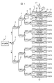
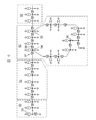
図1は本発明の実施例1を示す模式図である。1は超電導磁束量子回路(SFQ回路)であり、この出力である磁束量子信号を増幅するのが本発明の超電導信号増幅回路である。SFQ回路1の出力である磁束量子信号はジョセフソン伝送線路を通して第1段目の分岐回路2(SPで示す)に導入される。分岐回路2で2つになった磁束量子信号は、それぞれジョセフソン伝送線路(JTLで示す)3、4を介して第2段目のSP5、6に導入される。以下、図および説明が煩雑となるので、参照符号および説明は適宜省略した。第2段目の分岐回路5でさらに2つに分割された磁束量子信号はジョセフソン伝送線路7を介して第3段目の分岐回路8に導入され、ジョセフソン伝送線路9を介してさらに第4段目の分岐回路10に導入される。実施例1では第4段目の分岐回路10で最終的に2つに分割された磁束量子信号はジョセフソン伝送線路11、12を介してSQUID20、21の磁場印加用制御線22、23に導入される。説明を省略した分岐回路の他の線路も同様に構成される。したがって、実施例1では、4段の分岐回路を備えて、16個のSQUIDが直列接続されたものとなる。
【0019】
磁場印加用制御線22、23の先にはジョセフソン伝送線路13、14が接続されて、最終の終端抵抗15、16を介して接地される。17は電源であり、SQUIDにバイアス電流を供給する。直列に接続されたSQUIDおよび電源17の直列回路は両端で接地される。
【0020】
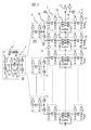
図2は、この等価回路を最上段と最下段の部分については全部を示し、途中は部分的に省略して示す。対応する構成要素に図1と同じ参照符号を付した。本等価回路での超電導磁束量子回路1は交流電源30によって磁束量子を発生する回路を例とした。超電導磁束量子回路1では、インダクタ31とジョセフソン接合33、34からなる超電導閉ループに交流電源30からジョセフソン接合35を介して交流電流が供給される。交流電源30の入力線の一方はインダクタ32を介してグラウンド37に接続され、交流電源30の他方もグラウンド37に接続されている。超電導閉ループに電流を流し込むことによって、超電導閉ループに磁束量子が1個発生する。ここで36は適当なバイアス電源でありジョセフソン接合33、34に適当な電流を流すために一端がジョセフソン接合33、34に、他端がグラウンド37に接続される。各ジョセフソン接合33、34の他端はグラウンド37に接続される。以下、本発明に係る超電導信号増幅回路の等価回路も回路素子は同じシンボルマークで表示したが、参照符号は適宜省略した。実施例1では、ジョセフソン接合はトンネル接合に抵抗を並列に接続したもの、あるいは電流−電圧特性に履歴を示さない接合のいずれを用いても良いが、本実施例では、電流−電圧特性に履歴を示さない接合を用いた。
【0021】
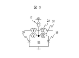
図3は、最上段のSQUID20に着目した等価回路の詳細図である。磁場印加用制御線22と磁気的に結合する入力用インダクタ38および2つのジョセフソン接合39により超電導閉ループ(SQUIDループインダクタ)が形成されている。
【0022】
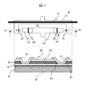
これらの超電導信号増幅回路および超電導磁束量子回路は酸化物超電導薄膜を用いて作製した。図4は図3に対応するSQUID20のレイアウトとIV−IVの位置で矢印方向に見た断面構造を示す模式図である。これを用いて回路の構造について説明する。La―Sr―Al―Ti酸化物の単結晶基板46上にY―Ba―Cu酸化物超電導薄膜で磁気遮蔽膜47を形成した。La―Sr―Al−Ti酸化物あるいはSr−Ti酸化物の層間絶縁膜48を介して、Y―Ba―Cu酸化物超電導薄膜を形成、これをインダクタ42および入力用インダクタ38ならびにジョセフソン接合41と結合部45の下部超電導電極とする。この上に連続してCe酸化物薄膜を形成、上下超電導電極の層間絶縁層40とする。下部超電導電極の斜面(エッジ)表面層をイオンビーム照射により、非晶質化したのち加熱して絶縁特性を生じさせ、これをジョセフソン接合のバリア層とする。さらにY―Ba―Cu酸化物超電導薄膜を形成、これを磁場印加用制御線22およびインダクタ43として使用する。入力用インダクタ38の端部とインダクタ43との結合部にジョセフソン接合41を形成する。インダクタ42と上部超電導電極で作られたインダクタ43との結合部45は、その幅をジョセフソン接合41の幅に対して十分大きくすることにより超電導接続を実現する。
【0023】
入力用インダクタ38とジョセフソン接合41および下部超電導電極で形成したインダクタ42、上部超電導電極で形成したインダクタ43により閉ループを形成する。各ジョセフソン接合41の臨界電流値は0.1mAから0.2mA、超電導閉ループのインダクタンスは10pHから20pHである。磁場印加用制御線22と入力用インダクタ38間の相互インダクタンスは5pHから15pHとした。抵抗素子は金薄膜を上下の超電導電極間に形成して作製した。
【0024】
分岐回路SPは、実施例1では、各段のジョセフソン伝送線路間を接続するインダクタである。この分岐回路をジョセフソン伝送線路とほぼ同じ構成として1本の入力線に対して2本の出力線を設け、かつ1個のジョセフソン接合と直流電流バイアス線を設けたものとしても良い。この場合、ジョセフソン接合の臨界電流値およびインダクタの大きさ等はジョセフソン伝送線路と同様とする。
【0025】
図5は実施例1に係る超電導信号増幅回路の動作を評価するために利用されたリング発振器を示すブロック図である。図2で説明した超電導磁束量子回路1では、本発明の狙いとするきわめて周波数の高い、パルス幅がピコ秒の磁束量子信号を発生することが実際上難しく、本発明の効果を確認できないので、図5に示すようなリング発振器で磁束量子信号を発生させ、この出力を実施例1に係る超電導信号増幅回路で増幅させて評価することとした。
【0026】
リング発振器は、発振起動入力部90、発振入力用ジョセフソン伝送線路91、ジョセフソン伝送線路リング92および出力用ジョセフソン伝送線路93が配列されている。発振起動入力部90は、図2で説明したSFQ回路1と同じ構成である。入力用ジョセフソン伝送線路91は、発振起動入力部90で発生した磁束量子信号が入力されると、これを次々に伝搬させる。ジョセフソン伝送線路リング92は、スプリッタとして機能する接続点94、95を2個、一方向性回路として機能するジョセフソン接合96を1個含む。入力用ジョセフソン伝送線路51からの磁束量子信号はインダクタ97を介してジョセフソン接合リング92の接続点94に入力されると、リングの両方向に分割されて伝搬されるが、インダクタ98の方向に伝搬された磁束量子信号のみがジョセフソン伝送線路リング92を次々と伝搬し、巡回するものとなる。巡回する磁束量子信号が接続点95に到達したときは、磁束量子信号は分割されて1つは出力用ジョセフソン伝送線路93に入力され、高速信号として利用される。
【0027】
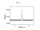
図6は、図5に示すリング発振器の出力を実施例1に係る超電導信号増幅回路に導入して、超電導信号増幅回路からの出力の周波数特性をスペクトル・アナライザで計測した結果を示す。超電導回路の動作温度は30Kであった。リング発振器からの発振出力周波数は、交流電源30の周波数あるいはジョセフソン接合へのバイアス電流の大きさを変えることにより、周波数10GHzから20GHzの範囲で制御できる。リング発振器からの磁束量子信号の出力は実施例1の信号増幅回路を通しても、周波数10GHzから20GHzでピークが検出された。検出された周波数スペクトルはリング発振器へのバイアス電流の大きさから想定される発振周波数と一致した。超電導信号増幅回路チップからスペクトル・アナライザまでの配線による減衰を考慮すれば、超電導信号増幅回路の出力電圧は5mV以上であった。リング発振器から出力される磁束量子信号の推定されるピーク電圧は、たかだか、0.3mV程度であり、本超電導信号増幅回路でSQUIDの数に対応して信号が増幅されていることがわかった。
【0028】
とくに周波数20GHz近くまで増幅作用を維持できたのはSQUIDの後ろにも磁場印加用制御線22,23の先にジョセフソン伝送線路を配置したことが寄与している。実施例2に述べるNb系超電導回路を想定して、ジョセフソン伝送線路を配置した場合と用いない場合のシミュレーションによる出力波形を図7に示した。磁場印加用制御線22,23の先にもジョセフソン伝送線路を配置した場合、波形の終了時間が5ps以上短くなっていることがわかる。これは1周期に換算すれば10psとなり、周波数特性の大幅な向上に資することがわかる。
【0029】
なお、実施例1のようにジョセフソン伝送線路を配置した場合には、SQUIDの出力電圧が一度急速に立ち上がった後、一旦低下している。これは、SQUIDの急速な電圧上昇に伴い、浮遊容量へのチャージが遅れて起こるための現象と言うことができる。これに対して、ジョセフソン伝送線路を持たない場合には、伝送遅れにより実施例1ほどの高速な立ち上がりでないために、SQUIDの出力電圧の上昇と浮遊容量へのチャージとが平行して起こっているため、立ち上がりが緩やかになってしまうが、一方では、SQUIDの出力電圧が一度急速に立ち上がった後、一旦低下すると言う現象は観察されない。
【0030】
(実施例2)
図8は、SQUIDの磁場検出感度を高めた本発明の実施例2の等価回路を図2と同じように示すものである。超電導信号増幅回路は超電導膜にNbを用いて作製した。デバイスはSiウェハ基板上に、Nb膜を超電導電極と磁気遮蔽膜に、Si酸化物薄膜を層間絶縁層に、Mo薄膜をシャント抵抗にするプロセスで作製した。ジョセフソン接合としては、Nb/AlOx/Nbトンネル接合を作製した。シャント抵抗はジョセフソン接合に並列に接続されており、ジョセフソン接合はヒステリシスを示さない特性のものとなる。しかし、図8では、図の表示を簡略化するために、シャント抵抗は示していない。また分岐回路は、本実施例でも図2と同様、ジョセフソン接合線路間を接続するインダクタである。
【0031】
図8の回路構成は、図2に示す実施例1のそれと本質的に同じであるが、最終段の分岐回路10で分割された磁束量子信号が導入される2つのSQUIDを一対とし、超電導閉ループ(SQUIDループインダクタ)のインダクタの一部を共有するとともに、共有部分の配線幅を広くすることにより、この部分のインダクタンスを小さくしたこと、および磁場印加用制御線がインダクタの共有部分とは異なるインダクタの部分と磁気的に結合していることが特徴である。
【0032】
図9は、最上段の一対のSQUID20、21に着目した等価回路の詳細図である。図10は図9に対応するSQUID20、21のレイアウトを示す模式図である。また、図11はSQUID20、21のレイアウトの端部とX−Xの位置で矢印方向に見た断面構造を示す模式図である。図9ではジョセフソン接合50、ジョセフソン接合50に並列に配置したシャント抵抗51を示した。SQUIDの回路パラメータは各ジョセフソン接合50の臨界電流値が0.1mA、接合のシャント抵抗51が4Ω、磁場印加用制御線22、23と結合する入力用インダクタ52、53は、長さが100ミクロンメートルで、各インダクタンスが7pH、2つのSQUIDが配線を共有するインダクタ54のインダクタンスは1pHである。電源電流は95%バイアスに相当する0.19mAとした。
【0033】
図9、図10および図11に示すSQUIDを以下説明する。Siウェハからなる基板46上にNbで作られたグランドを兼ねる磁気遮蔽膜47、Si酸化物薄膜による層間絶縁層48、Mo薄膜を用いたシャント抵抗51を作製したのち、層間絶縁膜56を形成する。一対の磁場印加用制御線22、23を上部超電導電極により形成するが、これに対応する位置に予め入力用インダクタ52、53と、これらの入力用インダクタ52、53とループを作る共有インダクタ54を両入力用インダクタ52、53に挟まれるように、下部超電導電極により形成する。入力用インダクタ52、53の端部と共有インダクタ54の端部との間を、上記Mo薄膜で形成したシャント抵抗51で接続する。層間絶縁膜を形成した後、ジョセフソン接合50を作製する下部電極の表面にAlの極薄酸化物薄膜を接合バリアとして作製した。さらに、磁場印加用制御線とジョセフソン接合50の上部電極を兼ねるNb薄膜を形成、Nb/AlOx/Nbトンネル接合を作製した。入力用インダクタ52、53とループを作る共有インダクタ54は、ジョセフソン接合50を介して、上部超電導電極で作ったインダクタ55で接続され、インダクタ55の他の端と共有インダクタ54の接続は超電導接続とする。シャント抵抗51はジョセフソン接合50に並列に接続されており、ジョセフソン接合50はヒステリシスを示さない特性のものとなる。この構造の製造プロセスは、特に説明するまでもなく、この分野の技術者によく知られている方法によればよい。
【0034】
この一対のSQUIDを8対、すなわち16個のSQUIDを図8に示したように直列に接続し、それぞれのSQUIDの磁場印加用制御線に磁束量子信号を同時に入力した時、一対のSQUID当たり0.24mVの出力電圧が得られた。この値は比較のために実施例1のように個々のSQUIDを直列に接続し、それぞれのSQUIDの制御線に磁束量子信号を同時に入力した場合の電圧、0.18mVに比べて30%大きいものであった。実施例2の構成によれば、実施例1の構成よりもより大きな増幅度が得られた。
【0035】
実施例2できわめて高い周波数でパルス幅がピコ秒の磁束量子信号の増幅を確認するために、実施例1と同様に、リング発振器で高速信号を発生させ、評価した結果、図6で説明した特性と同様の結果が得られた。しかしながら、リング発振器からの出力周波数を20GHzとした場合に、増幅後の検出信号のスペトルが広がり、高速信号に十分対応できていないことが示された。これは上に述べたように磁場印加用制御線を通過する磁束量子信号のパルス幅が広がったためである。
【0036】
(実施例3)
実施例2では、SQUIDの超電導閉ループのインダクタの一部を共有することで、磁場印加用制御線との相互インダクタンスを保ちながら、超電導閉ループのインダクタンスを低く抑えることができ、出力電圧を高めることができた。そこで、磁場印加用制御線22、23と入力用インダクタ52、53との磁気結合距離、すなわちSQUIDの横幅を実施例2の場合の100μmから80μmに20%短くした。これにより、実施例1と同じSQUIDの配置を採用した場合と同程度の増幅度を得るとともに、通過する磁束量子信号のパルス幅を、より狭く保つことができる。
【0037】
実施例3できわめて高い周波数の磁束量子信号の増幅を確認するために、実施例2と同様に、リング発振器で高速信号を発生させ、評価した結果、図6で説明した特性と同様に、リング発信器へのバイアス電流から想定される周波数と一致した。また、超電導回路チップからスペクトルアナライザまでの減衰を考慮して算出した出力電圧は1.5mV以上であった。周波数が20ギガHzの場合に、スペクトルの幅が狭くなった。一方、増幅度を少し下げてよければ、回路配列上の大きな要素を占めるSQUID部分の面積を少なくとも20%低減できることになる。
【0038】
(実施例4)
実施例1の等価回路をもつ超電導信号増幅回路の有効性を別の応用例で調べた。 図12に作製した超電導回路のブロック図を示す。8ビットのシフトレジスタ60と超電導信号増幅回路61を直列に接続するとともに、シフトレジスタ60を、クロックジェネレータとして用いた磁束量子信号列発生回路62の出力する磁束量子信号により駆動するものである。シフトレジスタ60にはデータ入力信号を別に加える。この超電導信号増幅回路61を実施例1で述べたものとほぼ同じ構成とし8ビットのシフトレジスタ60から得られる磁束量子信号を、図1または図2に示す分岐回路2に加えた。
【0039】
これらの超電導回路は実施例2の場合と同様に、超電導膜にNbを用いて作製した。このようにして作製した磁束量子信号列発生回路62、シフトレジスタ60および超電導信号増幅回路61から成る回路に100MHzから10GHzの周波数範囲で8ビットのデータ信号にクロック信号を同期させて入力した。磁束量子信号列発生回路62では10個の磁束量子列の間隔が20psとなるようにバイアス電流レベルを設定した。超電導信号増幅回路61からの出力をオシロスコープによって測定した結果、図13に示されるように、入力データと同じ信号列で、5mV以上に増幅された出力信号列が観察された。磁束量子信号の推定されるピーク高さは0.5mV程度であり、本超電導信号増幅回路で確かに高周波信号が増幅されていることがわかった。さらに本超電導信号増幅回路を用いることにより、シフトレジスタからの出力を雑音に埋もれさせることなく、比較的容易に取出して観測できることがわかった。
【0040】
超電導信号増幅回路61が実施例2あるいは実施例3に示されるものである場合でも、同様な好結果が得られることは言うまでも無い。
【0041】
(実施例5)
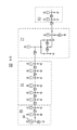
実施例5も、図12に示すように、8ビットのシフトレジスタ60と超電導信号増幅回路61を接続して超電導回路を作製した例である。実施例5では、磁束量子信号列発生回路62には、図14に示す回路を採用した。この磁束量子信号列発生回路は、図5で説明したリング発振器と対比してわかるように、リング回路92に代えて、入力信号を2個の出力線に交互に振分けるトグル・フリップ・フロップを基本とする回路63としたものである。回路63は、ジョセフソン接合64および65よりなる直列回路とジョセフソン接合66および67よりなる直列回路とが並列に接続されて、その一端に磁束量子信号が入力され、他端が接地される。並列接続された直列回路のそれぞれのジョセフソン接合の接続点間にはインダクタ68および69が接続されている。ジョセフソン接合64および66とインダクタ68および69が作る超電導ループ70は入力された磁束量子信号を蓄える働きをする。インダクタ68および69の接続点に、この超電導ループ70から信号を引出すために、インダクタ71、ジョセフソン接合72および73よりなる信号引出し線74が接続される。この信号引き出し線74の接続点は別に抵抗75を介して接地される。図に示すように、回路の必要な場所にはバイアス電流源が接続されている。信号引出し線74の2個のジョセフソン接合72、73の間からインダクタ76を介して磁束量子信号を引出す。回路63は磁束量子信号が出力される毎に超電導ループ70を周回する電流の向きが反転する。電流の反転にともなって連続的な信号の発生と停止が引き起こされる。1個の磁束量子信号入力によって磁束量子信号を発生し、つぎの1個の磁束量子信号によって磁束量子信号の発生を停止する。すなわち、入力の磁束量子信号を1/2の周波数に分周する。実施例5では、発振起動入力部90は交流入力により、磁束量子信号列を発生するものである。
【0042】
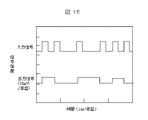
これらの超電導回路は超電導膜にNbを用いて作製した。100MHzから10GHzの周波数範囲で8ビットのデータ信号にクロック信号を同期させて入力した。超電導信号増幅回路からの出力をオシロスコープによって測定した結果、図15に示されるように、入力データと同じ信号列で、入力の磁束量子信号を1/2の周波数に分周するとともに、5mV以上に増幅された出力信号列が観察された。
【0043】
磁束量子信号の推定されるピーク高さは0.5mV以下であり、本超電導信号増幅回路で確かに高周波の磁束量子信号が増幅されていることがわかった。さらに本超電導信号増幅回路を用いることによって、シフトレジスタからの出力を雑音に埋もれさせることなく、比較的容易に取出して観測できることがわかった。
【0044】
(実施例6)
実施例6は、実施例5における磁束量子信号列発生回路を図16に示すように、より簡易化されたSFQ/dc変換回路77によるものとした他は実施例5と同じである。実施例1と同様に、周波数を10GHzから20GHzにして調べた結果、実施例6の増幅回路を通しても、周波数5GHzから10GHzでピークが検出された。周波数が1/2になっているのは、SFQ/dc変換回路を通したためである。検出された周波数の2倍の値はリング発振器へのバイアス電流から想定される発振周波数と一致した。また、超電導回路チップからスペクトル・アナライザまでの減衰を考慮して算出した出力電圧は1.5mV以上であった。リング発振器からの磁束量子信号の推定されるピーク高さは、たかだか、0.2mV程度であり、直列接続したSQUIDの数、16個に対応して信号が増幅されていることが分かった。
【0045】
これら実施例5および6は、SFQ回路のパルスが低速で、且つ急峻である場合に、見かけ上SFQ回路からのパルス間を連続する高速の急峻なパルスとして扱うのに有用なものである。
【0046】
(実施例7)
実施例7では、超電導量子干渉素子SQUIDは直列に接続するだけでなく、並列にも接続した。図17に、図1の分岐回路5より後段の部分のみを例示した。最終段の分岐回路から得られる2つの磁束量子信号の上側および下側のそれぞれの磁束量子信号を並列に配置したSQUIDの入力として加えるものとした。勿論、並列に配置されたSQUIDはすべて各列毎に直列接続される。実施例7では、図1と対比して明らかなように、SQUIDは合計16個配置されるが、直列に8列、並列に2列となる。また、SQUIDの磁場印加用制御線が構造上2倍の長さとなってしまう。
【0047】
このことは、本発明の特徴の一つであるSQUIDの出力側にジョセフソン伝送線路の配置によって磁束量子信号の急峻さが鈍るのを防止する効果を持たせても不利に作用する。すなわち、並列に配置されたSQUIDの出力のタイミングが異なるほか、磁場印加用制御線に加えられた先の磁束量子信号が抜けきらない内に次の磁束量子信号が磁場印加用制御線に加えられると言うような状況が起こる。その結果、図6で説明したような超高速特性を維持した増幅ができないことは明らかである。したがって、この実施例7は、前述の実施例より周波数の低い入力に対応して使用することで効果を発揮する。その場合には本増幅回路の入力側にSFQ/dc変換回路を設ける必要がある。
【0048】
これらの超電導回路は超電導薄膜にNbを用いて作製した。SQUIDに用いた超電導接合の臨界電流は0.2mAとした。実施例7による超電導信号増幅回路に実施例5の超電導回路から5GHzまでの周波数範囲で交流信号を入力した。超電導信号増幅回路からの出力をオシロスコープによって測定した結果、図18に示されるように、2mV以上に増幅され、周波数が入力交流信号の1/2となった出力波形が観察された。超電導量子干渉素子のバイアス電流は0.7mAであった。バイアス電流の大きさに比例して外部に取出せる電流が増加するため、素子を並列接続しない場合の2倍の出力電流となる。
【0049】
実施例7では、超電導回路からの出力信号周波数が低い場合、出力電流を増幅できることがわかった。超電導量子干渉素子の並列に配列する数は、最終段の分岐回路から伸びた1本の超電導線のインダクタが動作周波数を維持した状態で動作できる範囲内で増加できる。
【0050】
(実施例8)
実施例8の超電導信号増幅回路のSQUID列の回路パターンの模式図を図19に示す。図19は、図1、図2に示した信号増幅回路の最上段から3段部分と最下段から3段部分を具体的に示し、中間部は省略して示したものである。図19では、図1、図2に示したものと同じ物には同じ参照符号を付した。また、図は簡便のため、絶縁層については表示を省略し、必要な導電層と接続関係が分かるもののみを示している。
【0051】
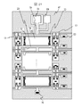
SQUID20、21、---は図4(a)で説明したように、超電導閉ループ(SQUIDループインダクタ)を下部超電導電極で作製した入力用インダクタ38およびインダクタ42、上部超電導電極で作製したインダクタ43で構成し、入力用インダクタ38とインダクタ43とはジョセフソン接合を形成し、インダクタ42とインダクタ43とは超電導接続となるように構成されている。入力用インダクタ38はSQUID20の磁場印加用制御線22と磁気的に結合するインダクタである。インダクタ42を形成する下部超電導電極はSQUID21のバイアス線を兼ねる。SQUID21以下についても、これらの関係が繰り返しパターンの形となっている。最下段のSQUIDの下部超電導電極で作られるインダクタ42は磁気遮蔽膜47と接続点78で接続され、接地されている。最上段のSQUID20の入力用インダクタ38は、バイアス電流供給線79に直結しており、バイアス電流供給線79は出力端子80および電源接続端子81に直結している。
【0052】
SQUID20の入力用インダクタ38には磁場印加用制御線22が絶縁膜を介して重ねて配列されている。図1、図2に示したように、磁場印加用制御線22はその入出力端にジョセフソン伝送線路11、13が設けられている。これらのジョセフソン伝送線路11、13は、磁場印加用制御線22と同じ上部超電導電極と下部超電導電極により形成される。ここで、下部超電導電極と上部超電導電極との間にはジョセフソン接合82が形成される。また、ジョセフソン伝送線路の下部超電導電極と磁気遮蔽膜47は超電導接続され、接地されている。さらに、磁場印加用制御線22は、金の抵抗層を介したのち、下部超電導電極83を介して磁気遮蔽膜47に接続され、接地されている。
【0053】
ここで注目すべき点は、実施例8では、最下段のSQUID以外のSQUIDは磁気遮蔽膜47を切り欠いた部分に形成されており、最下段のSQUIDの超電導閉ループのインダクタ42が全体領域の磁気遮蔽膜42に超電導接続されていることである。
【0054】
超電導磁束量子回路の周波数を低下させる最も大きな要因は、寄生容量である。動作周波数を高くするにしたがって、寄生容量の影響が増大する。SQUIDで、グランド電位の磁気遮蔽膜を用いた場合、層間絶縁膜を介してSQUIDのインダクタと磁気遮蔽膜間で容量が形成される。数十ミクロンの寸法の素子では容量は0.1pFから1pFの大きさになる。
【0055】
SQUIDが1段の場合、この寄生容量に蓄積される電荷は速度がピコ秒の動作に対してもとくに影響する大きさではない。しかしながら、SQUIDを多数段直列接続した場合、寄生容量は素子の個数に比例して増大するとともに、発生電圧が高くなるため、蓄積される電荷量はほぼ素子数の2乗に比例して増大する。従って、単純に、SQUIDの段数を16個とし、最大6mVの電圧を発生させるものとした場合、蓄積電荷は5フェムトクーロンから50フェムトクーロンとなる。一方蓄積電荷を供給するべきバイアス電流はSQUIDのバイアス条件から0.1mAから0.2mAで変わらないから、電荷の蓄積時間は25psから500psとなる。したがって出力の立ち上り時間がこれだけ増大することになる。
【0056】
一方、実施例8に係る超電導信号増幅回路によれば、大多数のSQUIDは磁気遮蔽膜を持たないためにこのような立ち上り時間の遅延要因は存在しない。容量成分はSQUIDのインダクタと制御線間に存在するが、交差する面積が相対的に小さいことと、層間絶縁膜が比較的厚いことから推定して、上記蓄積時間の1/20以下である。したがって実施例8になる超電導信号増幅回路では10GHz以上の高い周波数の信号を増幅し、出力することが可能であった。
【0057】
(実施例9)
実施例9の超電導信号増幅回路のSQUID列の回路パターンの模式図を図20に示す。図19と図20とを対比して明らかなように、実施例9では、最下段の超電導量子干渉素子以外のSQUIDの配置される全領域の磁気遮蔽膜47を切り欠いて除去してしまうのではなく、それぞれのSQUIDの部分のみに対応する磁気遮蔽膜84、85、---を形成するが、これらは周辺の磁気遮蔽膜47とは、分離されている。図23には図20のY−Yで示した位置で矢印方向に見た断面構造を示す。La−Sr−Al−Ti酸化物からなる基板46の上にY−Ba−Cu酸化物超電導体からなる磁気遮蔽膜47を形成後、SQUID列の各SQUID位置の磁気遮蔽膜85を周辺の磁気遮蔽膜47から切り離した。磁気遮蔽膜47および83の上にSr−Ti酸化物からなる絶縁膜48を形成、インダクタ42と磁気遮蔽膜83の間の電気的接続をとるためのホールを作製したのち、インダクタ38、42のためのY−Ba−Cu酸化物超電導電極を形成する。この後の接合作製は実施例1で示したものと同じである。
【0058】
ここでの特徴はSQUID21の下の磁気遮蔽膜84、85、---は周囲の磁気遮蔽膜47から分離されており、且つ、それぞれ接続点78を介してSQUIDのインダクタに電気的に接続されていることである。実施例9においても、超電導磁束量子回路の周波数を低下させることなく、また磁束量子パルスとほぼ同等の短く急峻な増幅信号を得られたが、実施例8においてのべたのと同じ理由によるものである。すなわちSQUIDのグランドとの浮遊容量成分をSQUIDのインダクタ38と磁場印加用制御線22間に限定できたからである。一方、実施例9のように、SQUIDにグランド電位から切離した磁気遮蔽膜を設けることにより、磁場印加用制御線22とSQUIDの入力用インダクタ間の磁気結合を高めることができた。したがって磁場印加用制御線22制御線の長さを短くすることができた。
【0059】
(実施例10)
実施例10の超電導信号増幅回路のSQUID列の回路パターンの模式図を図21に示す。図21は、図8に示した信号増幅回路の最上段と最下段の部分を具体的に示し、中間部は省略して示したものである。図21では、図8および図9−図11に示したものと同じ物には同じ参照符号を付した。また、図は簡便化のため、絶縁層については表示を省略し、必要な接続関係が分かるものを記載した。また、SQUIDについては、入力用インダクタ52、53および磁場印加用制御線22、23のみに参照符号を付した。超電導接合線路JTLに関しては、実施例8と同じ参照符号を付した。
【0060】
図21と図19を対照して明らかなように、実施例10と実施例8とは、実施例1と実施例2とが、一対の2つのSQUIDのインダクタの一部を共有したかしないかの差異があるのみである。なお、ジョセフソン伝送線路11、12のジョセフソン接合の部分の図面の表示が図21と図19とでは異なっているが、これは、図21では、ジョセフソン伝送線路11、12のジョセフソン接合を図11で詳細に説明した構造によるものであることを簡略化して示すためである。
【0061】
(実施例11)
実施例11の超電導信号増幅回路のSQUID列の回路パターンの模式図を図22に示す。図22と図21との対比は図20と図19との対比に対応するものであり、実施例10の磁気遮蔽膜を各SQUIDの対のそれぞれに分離して設けた点を除いては同じである。
【0062】
(その他の実施例)
上述の各実施例ではSQUIDの段数を16段としたが、段数を32段に増加し、増幅度を高めても追随できる周波数はほとんど低下しない。この理由は制御線が各々のSQUIDに繋がっているのみであるので、素子の段数を増加することによって磁場印加用制御線のインダクタンスが増加しないからである。ただし、超電導信号増幅回路の占める面積が大きくなり、チップ内の論理回路の大きさが制限される他、各要素回路の配置が難しくなる問題がある。
【0063】
【発明の効果】
発明によれば、数10ギガヘルツの高周波信号を、周波数を低減することなく電圧あるいは電流増幅できるのは勿論、波形の立ち上がり及び立ち下がり幅を広げることなく、任意の周波数の出力信号を増幅できる。
【図面の簡単な説明】
【図1】本発明の第1の実施例を示す模式図。
【図2】図1に示す実施例1の等価回路を示す図。
【図3】実施例1に採用したSQUIDの最上段に着目した等価回路の詳細図。
【図4】(a)は実施例1に採用したSQUIDのレイアウトを示す模式図、(b)は(a)のIV−IVの位置で矢印方向に見た断面構造を示す模式図。
【図5】実施例1に係る超電導信号増幅回路の動作を評価するために利用されたリング発振器を示すブロック図。
【図6】図5に示すリング発振器の出力を実施例1に係る超電導信号増幅回路に導入して、超電導回路の周波数特性をスペクトル・アナライザで計測した結果を示す図。
【図7】実施例2に述べるNb系超電導回路を想定して、ジョセフソン伝送線路を配置した場合と、用いない場合のシミュレーションによる出力波形を比較して示す図。
【図8】本発明の実施例2の等価回路を示す図。
【図9】超電導信号増幅回路をNb超電導膜等を用いて作製した実施例2のSQUIDの回路構成例を示す図。
【図10】図9のSQUIDの回路構成に対応する回路パターンの模式図。
【図11】(a)は実施例2に採用したSQUIDの端部のレイアウトを示す模式図、(b)は(a)のX−Xの位置で矢印方向に見た断面構造を示す模式図。
【図12】本発明の実施例4として超電導信号増幅回路をシフトレジスタの出力段に応用した構成を示すブロック図。
【図13】実施例4の超電導信号増幅回路からの出力をオシロスコープによって測定した結果の例を示す図。
【図14】実施例5で採用した磁束量子信号列発生回路の構成を示す図。
【図15】実施例5の超電導信号増幅回路からの出力をオシロスコープによって測定した結果の例を示す図。
【図16】実施例6で採用した磁束量子信号列発生回路の構成を示す図。
【図17】実施例7の超電導信号増幅回路の出力段の構成を示すブロック図。
【図18】実施例7の超電導信号増幅回路からの出力をオシロスコープによって測定した結果の例を示す図。
【図19】実施例8の超電導信号増幅回路のSQUID列の回路パターンの模式図。
【図20】実施例9の超電導信号増幅回路のSQUID列の回路パターンの模式図。
【図21】実施例10の超電導信号増幅回路のSQUID列の回路パターンの模式図。
【図22】実施例11の超電導信号増幅回路のSQUID列の回路パターンの模式図。
【図23】実施例9に採用したSQUIDのY−Yの位置で矢印方向に見た断面構造を示す模式図。
【符号の説明】
1:超電導磁束量子回路、 2,5,6,8,10:分岐回路(SP)、 3,4,7,9,11,12,13,14:ジョセフソン伝送線路、 20,21:超電導量子干渉素子(SQUID)、 22,23:磁場印加用制御線、 15,16:終端抵抗、 17:電源、 30:交流電源、 31,32,42,43,57,55,68,69,71,76,98:インダクタ、 33,34,35,39,41,50,64,65,66,67,72,73,82,96:ジョセフソン接合、 37:グラウンド、 36:バイアス電源、 38,52,53:入力用インダクタ、 40,48,56,57:絶縁層、 45:結合部、 46:基板、 47,84,85:磁気遮蔽膜、 51:シャント抵抗、 54:共有インダクタ、 60:シフトレジスタ、 61:超電導信号増幅回路、 62:磁束量子信号列発生回路、 63:回路、 70:超電導ループ、 74:信号引出し線、 75:抵抗、 77:SFQ/dc変換回路、 78,94,95:接続点、 79:バイアス電流供給線、 80:出力端子、 81:電源接続端子、 90:発振起動入力部、 91:入力用ジョセフソン伝送線路、 92:ジョセフソン伝送線路リング、 93:出力用ジョセフソン伝送線路。[0001]
BACKGROUND OF THE INVENTION
The present invention relates to the field of superconducting electronics that uses superconducting properties and exhibits ultrafast switching performance in high-speed digital, analog data processing circuits, etc., and is particularly essential for superconducting circuits that use single flux quanta as an information carrier. The present invention relates to a configuration of a superconducting circuit for signal amplification.
[0002]
[Prior art]
A single flux quantum (hereinafter abbreviated as SFQ) is a carrier of information, that is, a superconducting flux quantum circuit (SFQ circuit) in which the presence or absence of SFQ is 1, 0, and the signal width is picoseconds. It is an ultra-high speed circuit that can transmit at a frequency exceeding 100 gigahertz. Applications to analog-to-digital conversion circuits and digital logic circuits that take advantage of high speed have been studied. However, the signal amplitude of the superconducting magnetic flux quantum circuit is weak, and an output voltage of 1 mV or less can be obtained at most. The small signal level has the advantage of low power consumption and heat generation during operation. However, in practical use of the SFQ circuit, connection with a normal semiconductor circuit such as CMOS is essential, and it is necessary to amplify the output voltage of the superconducting flux quantum circuit up to the operating voltage of the circuit to which the signal is transferred. There is. In addition, when wiring is provided from a superconducting circuit placed in a cryogenic container to a circuit in a room temperature environment, the wiring becomes long and the signal tends to attenuate. From this point as well, the signal is amplified at the output of the superconducting circuit. Must be placed on the circuit.
[0003]
Conventional superconducting signal amplifying circuits are classified into a type in which series Josephson junctions are simultaneously switched to a voltage state and a type in which a superconducting quantum interference element (hereinafter abbreviated as SQUID) is used. Here, the superconducting quantum interference device (SQUID) includes two Josephson junctions in a superconducting closed loop made of superconducting wiring, and a bias current input terminal is provided between the two Josephson junctions, and a ground terminal is provided between the other. In other words, it is an element in which a large voltage change occurs between both terminals with respect to an extremely weak magnetic field change.
[0004]
An example of using SQUID and supporting ultra-high-speed signal amplification is Mukarnov et al., IEE Transactions Applied Superconductivity, Vol. 7, p. 2826, 1997 (OA Mukhanov et. al., IEEE Transactions on Applied Superconductivity, Vol. 7, P. 2826, 1997). In this example, by connecting a Josephson transmission line, the magnetic flux quantum signal is branched into a plurality of magnetic flux quantum signals while maintaining the pulse signal characteristics, and the magnetic field application of each SQUID of the SQUID sequence connected in series is performed. This is a method of inputting to the control line. Here, in the Josephson transmission line, two or more Josephson junctions are connected in parallel by a superconducting wiring, one end is grounded, a bias power source is connected to a wiring connecting the other end, and a magnetic flux quantum signal is propagated to the wiring. Is. When the magnetic flux quantum signal is input, the Josephson junction is sequentially switched, and the magnetic flux quantum signal propagates while shaping the pulse waveform.
[0005]
By branching the magnetic flux quantum signal when inputting to the SQUID, the length of the control line of the SQUID becomes shorter than that of a single control line, and the signal delay proportional to the magnitude of the control line inductance is reduced. Yes. As a result, an 8 GHz signal is amplified to 2 mV.
[0006]
On the other hand, I.E.E.E. Transactions Applied Superconductivity such as Polonsky, Vol. 7, p. 2818, 1997 (S. Polonsky et al., IEEE Transactions on Applied Superconductivity, Vol. 7, P. 2818, 1997). This is because it is necessary to resolve the impedance mismatch caused by the wiring on the substrate in the signal transmission between the superconducting chips. Therefore, a single flux quantum signal (here, four) signals (four in this case) Multi-Flux Quantum). The circuit of FIG. 3 of this document also discloses that SQUIDs are switched simultaneously by assembling branch circuits in cascade.
[0007]
[Problems to be solved by the invention]
An object of the present invention is to amplify a magnetic flux quantum signal exceeding several tens of gigahertz or 100 gigahertz of a superconducting magnetic flux quantum circuit. Specifically, obtaining an amplification degree, maintaining high speed, An object of the present invention is to provide a superconducting signal amplifier circuit capable of improving the response to a signal.
[0008]
[Means for Solving the Problems]
In the superconducting signal amplifier circuit of the present invention, a plurality of SQUIDs connected in series are arranged, and a magnetic flux quantum signal maintaining a pulse characteristic is simultaneously input to the magnetic field application control line of each SQUID, and the SQUID is magnetically coupled. By doing so, the SQUID is simultaneously switched to the voltage state. That is, a first Josephson junction pair composed of two Josephson junctions, and first and second inductive elements that are annularly connected to the first Josephson junction pair to form a first superconducting loop. A second Josephson junction pair consisting of two Josephson junctions that share a part of the second inductive element and are connected in a ring and form a second superconducting loop; and the second Josephson There is provided a superconducting quantum interference device comprising a third inductive element forming a second superconducting loop annularly connected to the junction pair, and an input circuit magnetically coupled to the first and third inductive elements. Also, an inductive element having an input end for inputting a signal and an output end for outputting a signal, a Josephson junction connected to the input end and the output end of the inductive element, and connected to the input end and the output end A first Josephson transmission line, a second Josephson transmission line having the same structure as the first Josephson transmission line, and an input end of the second Josephson transmission line And a first inductive element connected between the output terminal of the first Josephson transmission line, a first inductive element magnetically coupled to the fourth inductive element, and two A Josephson junction pair consisting of the Josephson junction, the Josephson junction pair and the fourth inductive element connected in a ring, and a first superconducting loop, and an output end of the second Josephson transmission line Consisting of connected resistance members Give the conductivity circuit. Furthermore, the substrate, the magnetic shielding film provided on the substrate, the first insulating film electrically insulated on the magnetic shielding film, and the first provided on the first insulating film. A superconducting thin film, a second insulating film provided on the first superconducting thin film, a second superconducting thin film provided on the second insulating film, the first superconducting thin film, A superconducting circuit having a Josephson junction formed by connecting two superconducting thin films is provided, and a superconducting circuit having a plurality of the superconducting circuits and having the magnetic shielding film separated in units of the superconducting circuits is provided. In terms of mounting, a substrate, a magnetic shielding film provided on the substrate, a first insulating film electrically insulated on the magnetic shielding film, and an upper portion of the first insulating film are provided. A first superconducting thin film, a second insulating film provided on the first superconducting thin film, a second superconducting thin film provided on the second insulating film, and the first superconducting thin film. This is made possible by the structure of a superconducting circuit including a superconducting circuit having a Josephson junction formed by connecting a superconducting thin film and a second superconducting thin film, and two superconducting thin films magnetically coupled to the superconducting circuit. From another viewpoint, a substrate, a magnetic shielding film provided on the substrate, a first insulating film electrically insulated on the magnetic shielding film, and an upper portion of the first insulating film A first superconducting thin film provided; a second insulating film provided on the first superconducting thin film; a second superconducting thin film provided on the second insulating film; and the first superconducting thin film. A superconducting circuit having a Josephson junction formed by connecting the superconducting thin film and the second superconducting thin film, two superconducting thin films magnetically coupled to the superconducting circuit, and a plurality of the superconducting circuits and the magnetic shielding film Provides a superconducting circuit that is separated in units of the superconducting circuit.
[0009]
Further, as a circuit configuration of low noise as a circuit system, a first Josephson junction pair composed of two Josephson junctions and an annular connection with the first Josephson junction pair form a first superconducting loop. A second Josephson junction comprising a first inductive element, a second inductive element, and two Josephson junctions that share the second inductive element and are annularly connected to form a second superconducting loop A son junction pair, a third inductive element forming a second superconducting loop annularly connected to the second Josephson junction pair, an input end for inputting a signal, and an output end for outputting a signal. A first Josephson transmission line comprising: an inductive element having: a Josephson junction connected to an input terminal and an output terminal of the inductive element; and a DC power source connected to the input terminal and the output terminal; Said first joseph A second Josephson transmission line having the same configuration as the Son transmission line, and a fourth inductive element connected to the input end of the first Josephson transmission line and magnetically coupled to the first inductive element And a fifth inductive element magnetically coupled to the third inductive element connected to the input end of the second Josephson transmission line, and an output end of the first Josephson transmission line. In addition, a superconducting circuit element can be achieved by having the second termination resistor connected to the output terminal of the first termination resistor and the second Josephson transmission line.
[0010]
Further, as a configuration for simultaneously inputting a signal and obtaining a high amplification factor, a first Josephson junction pair composed of two Josephson junctions and a first Josephson junction pair connected in a ring shape are connected in a ring shape. A first inductive element and a second inductive element that form one superconducting loop, and two Josephsons that share the second inductive element and are annularly connected to form a second superconducting loop A second Josephson junction pair formed of a junction, a third inductive element forming a second superconducting loop connected in a ring with the second Josephson junction pair, an input terminal for inputting a signal, and a signal And a first power source connected to the input end and the output end of the inductive element, and a direct current power source connected to the input end and the output end. Josephson transmission line of the A second Josephson transmission line having the same configuration as that of the first Josephson transmission line, a fourth inductive element magnetically coupled to the first inductive element, and an output end of the first Josephson transmission line The fourth inductive element is connected to the fifth inductive element magnetically coupled to the third inductive element, and the fifth inductive element is connected to the output end of the second Josephson transmission line. A sixth inductive element connected to the input end of the first Josephson transmission line, and a seventh inductive element connected to the input end of the second Josephson transmission line. It is possible to achieve a superconducting circuit by providing a signal input terminal connecting one end of the sixth inductive element and one end of the seventh inductive element.
[0011]
DETAILED DESCRIPTION OF THE INVENTION
The present invention has dealt with increasing the degree of amplification, which is the first problem, by increasing the sensitivity of each SQUID to magnetic flux quanta. In order to increase the magnetic field sensitivity of the SQUID, the inductance of the inductor forming the superconducting closed loop of the SQUID is reduced, and the two SQUID inductors are combined so that the coupling distance between the magnetic field application control line and the SQUID inductor can be increased. A shared structure was adopted. A structure in which two SQUIDs share a part of an inductor for the purpose of increasing the magnetic field detection sensitivity is also shown in Japanese Patent Laid-Open No. 8-236824. In this example, an input signal is magnetically coupled to a shared inductor. On the other hand, in the present invention, two magnetic flux quantum signals having a constant size are magnetically coupled to two SQUIDs. In the present invention, a non-shared inductor part is used as an input inductor and magnetically coupled. .
[0012]
When the SQUID becomes highly sensitive, the coupling distance between the magnetic field application control line and the SQUID input inductor can be shortened, that is, the inductance of the control line can be reduced, and the pulse waveform of the magnetic flux quantum signal passing therethrough can be prevented from becoming dull. It is also effective for maintaining the high speed, which is the next second problem.
[0013]
In response to the high speed of the second problem of the above problem, in the present invention, branch circuits that generate two flux quanta from one flux quantum are provided in cascade, and flux quantum signals are generated by the number of SQUIDs. . Josephson transmission lines between all branch circuits are used to maintain pulse characteristics, and each branch transmission line is provided with the same number of branch circuits and the same number of Josephson transmission lines, and the route of flux quantum signals Even if they are taken, the substantial length of the line is the same, that is, the flux quantum signal reaches all the SQUIDs simultaneously. Furthermore, in the present invention, a Josephson transmission line is also arranged on the exit side of the SQUID magnetic field application control line, and then terminated with a resistor. The Josephson transmission line arranged on the exit side prevents signal reflection and prevents the waveform of the magnetic flux quantum signal passing through the control line of the SQUID from dulling. The Josephson transmission line on the exit side is particularly effective during high-frequency operation exceeding 10 GHz.
[0014]
In addition, when it is necessary to deal with a low-frequency, that is, magnetic flux quantum signal having a wide interval on the time axis, in the present invention, an SFQ / dc conversion circuit is provided at the input of the superconducting signal amplifier circuit, and a pulse signal is transmitted. A pseudo level signal is used.
[0015]
In response to the responsiveness of the third problem of the above problem, in the present invention, the magnetic shielding film is removed from most of the SQUID column regions connected in series in the superconducting signal amplifier circuit. Or it was set as the structure which isolate | separated the magnetic shielding film of the area | region corresponding to each SQUID connected in series from other magnetic shielding films. The reason for this will be described below.
[0016]
In general, since the magnetic shielding film also serves as a circuit ground, a capacitance exists between the SQUID and the magnetic shielding film. As the output voltage increases, the influence of this capacitance increases, and the response characteristics of the amplified signal with respect to the input signal deteriorate. This is because it takes a long time to charge the capacitance when the bias current of the SQUID that also serves as the power supply to the output signal is a small current value (0.1 to 0.2 mA).
[0017]
Hereinafter, the present invention will be described based on examples described below.
[0018]
(Example 1)
FIG. 1 is a schematic diagram showing Example 1 of the present invention.
[0019]
[0020]
FIG. 2 shows the entire equivalent circuit in the uppermost and lowermost parts, with the middle part partially omitted. Corresponding components are assigned the same reference numerals as in FIG. The superconducting magnetic
[0021]
FIG. 3 is a detailed diagram of an equivalent circuit focusing on the
[0022]
These superconducting signal amplification circuits and superconducting flux quantum circuits were fabricated using oxide superconducting thin films. FIG. 4 is a schematic diagram showing a
[0023]
A closed loop is formed by the
[0024]
In the first embodiment, the branch circuit SP is an inductor that connects the Josephson transmission lines at each stage. The branch circuit may have substantially the same configuration as the Josephson transmission line, two output lines may be provided for one input line, and one Josephson junction and a direct current bias line may be provided. In this case, the critical current value of the Josephson junction, the size of the inductor, and the like are the same as those of the Josephson transmission line.
[0025]
FIG. 5 is a block diagram showing a ring oscillator used for evaluating the operation of the superconducting signal amplifier circuit according to the first embodiment. In the superconducting magnetic
[0026]
In the ring oscillator, an oscillation
[0027]
FIG. 6 shows the result of introducing the output of the ring oscillator shown in FIG. 5 into the superconducting signal amplifier circuit according to Example 1 and measuring the frequency characteristics of the output from the superconducting signal amplifier circuit with a spectrum analyzer. The operating temperature of the superconducting circuit was 30K. The oscillation output frequency from the ring oscillator can be controlled in the frequency range of 10 GHz to 20 GHz by changing the frequency of the
[0028]
In particular, the amplification effect can be maintained up to a frequency close to 20 GHz because the Josephson transmission line is arranged behind the SQUID and beyond the magnetic field
[0029]
When the Josephson transmission line is arranged as in the first embodiment, the output voltage of the SQUID once rises rapidly and then temporarily decreases. This can be said to be a phenomenon caused by a delay in the charge to the stray capacitance with the rapid increase in the voltage of the SQUID. On the other hand, when there is no Josephson transmission line, the rise in the output voltage of the SQUID and the charge to the stray capacitance occur in parallel because the transmission delay does not cause the rise as fast as in the first embodiment. Therefore, the rise becomes gentle, but on the other hand, the phenomenon that the output voltage of the SQUID once rises rapidly and then decreases is not observed.
[0030]
(Example 2)
FIG. 8 shows an equivalent circuit of the second embodiment of the present invention in which the magnetic field detection sensitivity of the SQUID is increased as in FIG. The superconducting signal amplifier circuit was fabricated using Nb for the superconducting film. The device was fabricated on a Si wafer substrate by a process in which an Nb film was used as a superconducting electrode and a magnetic shielding film, an Si oxide thin film was used as an interlayer insulating layer, and an Mo thin film was used as a shunt resistor. As the Josephson junction, an Nb / AlOx / Nb tunnel junction was fabricated. The shunt resistor is connected in parallel to the Josephson junction, and the Josephson junction has a characteristic that exhibits no hysteresis. However, in FIG. 8, the shunt resistor is not shown in order to simplify the display of the figure. The branch circuit is an inductor that connects the Josephson junction lines in this embodiment as in FIG.
[0031]
The circuit configuration of FIG. 8 is essentially the same as that of the first embodiment shown in FIG. 2, but a pair of two SQUIDs into which the magnetic flux quantum signals divided by the
[0032]
FIG. 9 is a detailed diagram of an equivalent circuit focusing on the pair of
[0033]
The SQUID shown in FIGS. 9, 10, and 11 will be described below. A
[0034]
When eight pairs of SQUIDs, that is, 16 SQUIDs are connected in series as shown in FIG. 8 and magnetic flux quantum signals are simultaneously input to the magnetic field application control lines of the respective SQUIDs, 0 per pair of SQUIDs. An output voltage of .24 mV was obtained. For comparison, this value is 30% larger than the voltage of 0.18 mV when individual SQUIDs are connected in series as in Example 1 and magnetic flux quantum signals are simultaneously input to the control lines of the respective SQUIDs. Met. According to the configuration of Example 2, a greater amplification degree than that of Example 1 was obtained.
[0035]
In order to confirm the amplification of a magnetic flux quantum signal having a very high frequency and a pulse width of picoseconds in Example 2, a high-speed signal was generated and evaluated in the same manner as in Example 1, and the result was described with reference to FIG. Similar results to the characteristics were obtained. However, when the output frequency from the ring oscillator is set to 20 GHz, the spectrum of the detection signal after amplification spreads, indicating that the high-speed signal cannot be sufficiently handled. This is because the pulse width of the magnetic flux quantum signal passing through the magnetic field application control line has increased as described above.
[0036]
(Example 3)
In the second embodiment, by sharing a part of the inductor of the SQUID superconducting closed loop, the inductance of the superconducting closed loop can be kept low while maintaining the mutual inductance with the magnetic field application control line, and the output voltage can be increased. did it. Therefore, the magnetic coupling distance between the magnetic field
[0037]
In order to confirm the amplification of the very high frequency magnetic flux quantum signal in the third embodiment, a high-speed signal is generated by a ring oscillator and evaluated in the same manner as in the second embodiment. As a result, as in the characteristics described in FIG. It agreed with the frequency assumed from the bias current to the transmitter. The output voltage calculated in consideration of the attenuation from the superconducting circuit chip to the spectrum analyzer was 1.5 mV or more. When the frequency was 20 gigahertz, the spectrum width was narrowed. On the other hand, if the degree of amplification is slightly reduced, the area of the SQUID portion that occupies a large element on the circuit arrangement can be reduced by at least 20%.
[0038]
Example 4
The effectiveness of the superconducting signal amplifier circuit having the equivalent circuit of Example 1 was examined in another application example. FIG. 12 shows a block diagram of the manufactured superconducting circuit. An 8-
[0039]
These superconducting circuits were produced using Nb for the superconducting film, as in Example 2. A clock signal was synchronized with an 8-bit data signal in a frequency range of 100 MHz to 10 GHz in the circuit composed of the magnetic flux quantum signal string generation circuit 62, the
[0040]
Needless to say, the same good results can be obtained even when the superconducting
[0041]
(Example 5)
Example 5 is also an example in which a superconducting circuit is fabricated by connecting an 8-
[0042]
These superconducting circuits were produced using Nb for the superconducting film. A clock signal was input in synchronization with an 8-bit data signal in a frequency range of 100 MHz to 10 GHz. As a result of measuring the output from the superconducting signal amplification circuit with an oscilloscope, as shown in FIG. 15, the input magnetic flux quantum signal is divided into ½ frequency with the same signal sequence as the input data, and is increased to 5 mV or more. An amplified output signal train was observed.
[0043]
The estimated peak height of the magnetic flux quantum signal is 0.5 mV or less, and it was found that the high frequency magnetic flux quantum signal was certainly amplified by this superconducting signal amplifier circuit. Furthermore, it was found that by using this superconducting signal amplifier circuit, the output from the shift register can be taken out and observed relatively easily without being buried in noise.
[0044]
(Example 6)
The sixth embodiment is the same as the fifth embodiment except that the magnetic flux quantum signal sequence generation circuit in the fifth embodiment is based on a simplified SFQ / dc conversion circuit 77 as shown in FIG. As in Example 1, as a result of examining the frequency from 10 GHz to 20 GHz, a peak was detected at a frequency of 5 GHz to 10 GHz even through the amplifier circuit of Example 6. The reason why the frequency is ½ is that the SFQ / dc conversion circuit is passed. The value twice the detected frequency coincided with the oscillation frequency assumed from the bias current to the ring oscillator. Further, the output voltage calculated in consideration of the attenuation from the superconducting circuit chip to the spectrum analyzer was 1.5 mV or more. The estimated peak height of the magnetic flux quantum signal from the ring oscillator is at most about 0.2 mV, and it was found that the signal was amplified corresponding to the number of SQUIDs connected in series, ie 16 pieces.
[0045]
The fifth and sixth embodiments are useful for treating the pulses from the SFQ circuit as continuous high-speed and steep pulses when the pulses of the SFQ circuit are low-speed and steep.
[0046]
(Example 7)
In Example 7, the superconducting quantum interference device SQUID was connected not only in series but also in parallel. FIG. 17 illustrates only the portion subsequent to the
[0047]
This is disadvantageous even if the effect of preventing the steepness of the flux quantum signal from being dulled by the arrangement of the Josephson transmission line on the output side of the SQUID, which is one of the features of the present invention. In other words, the output timing of the SQUIDs arranged in parallel is different, and the next magnetic flux quantum signal is applied to the magnetic field application control line before the previous magnetic flux quantum signal applied to the magnetic field application control line can be completely removed. This happens. As a result, it is obvious that the amplification cannot be performed while maintaining the ultra-high speed characteristic as described in FIG. Therefore, the seventh embodiment is effective when used corresponding to an input having a lower frequency than the above-described embodiments. In that case, it is necessary to provide an SFQ / dc conversion circuit on the input side of the amplifier circuit.
[0048]
These superconducting circuits were produced using Nb for the superconducting thin film. The critical current of the superconducting junction used for the SQUID was 0.2 mA. An AC signal was input to the superconducting signal amplifier circuit according to Example 7 in the frequency range from the superconducting circuit of Example 5 to 5 GHz. As a result of measuring the output from the superconducting signal amplification circuit with an oscilloscope, as shown in FIG. 18, an output waveform amplified to 2 mV or more and having a frequency half that of the input AC signal was observed. The bias current of the superconducting quantum interference device was 0.7 mA. Since the current that can be extracted to the outside increases in proportion to the magnitude of the bias current, the output current is twice that when the elements are not connected in parallel.
[0049]
In Example 7, it was found that the output current can be amplified when the output signal frequency from the superconducting circuit is low. The number of superconducting quantum interference elements arranged in parallel can be increased within a range in which the inductor of one superconducting wire extending from the final branch circuit can operate while maintaining the operating frequency.
[0050]
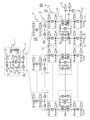
(Example 8)
FIG. 19 shows a schematic diagram of the circuit pattern of the SQUID column of the superconducting signal amplifier circuit according to the eighth embodiment. FIG. 19 specifically shows the three-stage portion from the uppermost stage and the three-stage portion from the lowermost stage of the signal amplifier circuit shown in FIGS. 1 and 2, and the intermediate portion is omitted. In FIG. 19, the same components as those shown in FIGS. 1 and 2 are denoted by the same reference numerals. Further, for the sake of simplicity, the illustration of the insulating layer is omitted, and only those showing the necessary conductive layer and connection relationship are shown.
[0051]
As shown in FIG. 4A,
[0052]
A magnetic field
[0053]
What should be noted here is that in Example 8, SQUIDs other than the lowest SQUID are formed in the notched portion of the
[0054]
The biggest factor that reduces the frequency of the superconducting flux quantum circuit is the parasitic capacitance. As the operating frequency is increased, the influence of parasitic capacitance increases. When a magnetic shielding film having a ground potential is used in the SQUID, a capacitance is formed between the SQUID inductor and the magnetic shielding film via an interlayer insulating film. In an element having a size of several tens of microns, the capacitance is 0.1 pF to 1 pF.
[0055]
When the SQUID is one stage, the charge accumulated in the parasitic capacitance is not so large as to affect the operation at picosecond speed. However, when multiple SQUIDs are connected in series, the parasitic capacitance increases in proportion to the number of elements and the generated voltage increases, so that the amount of accumulated charge increases in proportion to the square of the number of elements. . Therefore, if the number of SQUID stages is 16 and a voltage of 6 mV at maximum is generated, the accumulated charge is 5 femtocoulombs to 50 femtocoulombs. On the other hand, since the bias current for supplying the accumulated charge does not change from 0.1 mA to 0.2 mA from the bias condition of the SQUID, the charge accumulation time is 25 ps to 500 ps. Therefore, the output rise time is increased by this amount.
[0056]
On the other hand, according to the superconducting signal amplifier circuit according to the eighth embodiment, since the majority of SQUIDs do not have a magnetic shielding film, such a rise time delay factor does not exist. The capacitance component exists between the SQUID inductor and the control line, but is less than 1/20 of the above accumulation time, presumed that the intersecting area is relatively small and the interlayer insulating film is relatively thick. Therefore, the superconducting signal amplifier circuit according to the eighth embodiment can amplify and output a signal having a high frequency of 10 GHz or more.
[0057]
Example 9
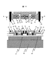
FIG. 20 shows a schematic diagram of the circuit pattern of the SQUID column of the superconducting signal amplifier circuit according to the ninth embodiment. As is clear by comparing FIG. 19 and FIG. 20, in Example 9, the
[0058]
The feature here is that the
[0059]
(Example 10)
FIG. 21 shows a schematic diagram of the circuit pattern of the SQUID string of the superconducting signal amplifier circuit according to the tenth embodiment. FIG. 21 specifically shows the uppermost and lowermost portions of the signal amplifier circuit shown in FIG. 8, with the intermediate portion omitted. In FIG. 21, the same components as those shown in FIGS. 8 and 9 to 11 are denoted by the same reference numerals. Further, for the sake of simplification, the illustration of the insulating layer is omitted and the necessary connection relationship can be understood. For SQUID, only the
[0060]
As is clear from FIG. 21 and FIG. 19, in the tenth and eighth embodiments, whether the first and second embodiments share part of a pair of two SQUID inductors or not. There is only a difference. In addition, although the display of the figure of the Josephson junction part of
[0061]
(Example 11)
A schematic diagram of the circuit pattern of the SQUID string of the superconducting signal amplifier circuit of Example 11 is shown in FIG. The comparison between FIG. 22 and FIG. 21 corresponds to the comparison between FIG. 20 and FIG. 19, and is the same except that the magnetic shielding film of Example 10 is provided separately for each SQUID pair. It is.
[0062]
(Other examples)
In each of the above-described embodiments, the number of SQUID stages is set to 16, but the number of stages can be increased to 32, and the frequency that can be followed is hardly lowered even if the amplification degree is increased. This is because the control line is only connected to each SQUID, and the inductance of the magnetic field application control line does not increase by increasing the number of element stages. However, the area occupied by the superconducting signal amplifier circuit is increased, which limits the size of the logic circuit in the chip and makes it difficult to arrange the element circuits.
[0063]
【The invention's effect】
According to the invention, a high frequency signal of several tens of gigahertz can be amplified with voltage or current without reducing the frequency, and an output signal with an arbitrary frequency can be amplified without widening the rising and falling widths of the waveform.
[Brief description of the drawings]
FIG. 1 is a schematic diagram showing a first embodiment of the present invention.
FIG. 2 is a diagram showing an equivalent circuit of the first embodiment shown in FIG.
FIG. 3 is a detailed diagram of an equivalent circuit focusing on the topmost SQUID employed in the first embodiment.
4A is a schematic diagram showing a layout of a SQUID employed in Example 1, and FIG. 4B is a schematic diagram showing a cross-sectional structure viewed in the direction of an arrow at the position IV-IV in FIG.
FIG. 5 is a block diagram showing a ring oscillator used for evaluating the operation of the superconducting signal amplifier circuit according to the first embodiment.
6 is a diagram showing the result of measuring the frequency characteristic of the superconducting circuit with a spectrum analyzer by introducing the output of the ring oscillator shown in FIG. 5 into the superconducting signal amplifier circuit according to Example 1. FIG.
FIG. 7 is a diagram showing a comparison of output waveforms obtained by simulation when a Josephson transmission line is disposed and when a Josephson transmission line is not used, assuming an Nb-based superconducting circuit described in the second embodiment.
FIG. 8 is a diagram showing an equivalent circuit of
FIG. 9 is a diagram showing a circuit configuration example of a SQUID of Example 2 in which a superconducting signal amplifier circuit is manufactured using an Nb superconducting film or the like.
10 is a schematic diagram of a circuit pattern corresponding to the circuit configuration of the SQUID of FIG.
11A is a schematic diagram showing a layout of an end portion of a SQUID employed in Example 2, and FIG. 11B is a schematic diagram showing a cross-sectional structure viewed in the direction of an arrow at the position XX in FIG. .
FIG. 12 is a block diagram showing a configuration in which a superconducting signal amplifier circuit is applied to an output stage of a shift register as
FIG. 13 is a diagram showing an example of a result obtained by measuring an output from the superconducting signal amplifier circuit according to the fourth embodiment with an oscilloscope.
14 is a diagram illustrating a configuration of a magnetic flux quantum signal train generation circuit employed in Example 5. FIG.
FIG. 15 is a diagram illustrating an example of a result obtained by measuring an output from a superconducting signal amplifier circuit according to Example 5 with an oscilloscope;
FIG. 16 is a diagram showing a configuration of a magnetic flux quantum signal train generation circuit employed in Example 6;
FIG. 17 is a block diagram showing the configuration of the output stage of the superconducting signal amplifier circuit according to the seventh embodiment.
FIG. 18 is a diagram showing an example of a result obtained by measuring an output from the superconducting signal amplifier circuit according to the seventh embodiment with an oscilloscope.
FIG. 19 is a schematic diagram of a circuit pattern of a SQUID string of the superconducting signal amplifier circuit according to the eighth embodiment.
20 is a schematic diagram of a circuit pattern of a SQUID column of the superconducting signal amplifier circuit according to
FIG. 21 is a schematic diagram of a circuit pattern of a SQUID column of the superconducting signal amplifier circuit according to the tenth embodiment;
22 is a schematic diagram of a circuit pattern of a SQUID column of the superconducting signal amplifier circuit according to
23 is a schematic diagram showing a cross-sectional structure viewed in the direction of the arrow at the YY position of the SQUID employed in Example 9. FIG.
[Explanation of symbols]
1: Superconducting flux quantum circuit 2, 5, 6, 8, 10: Branch circuit (SP) 3, 4, 7, 9, 11, 12, 13, 14: Josephson transmission line 20, 21: Superconducting quantum Interference element (SQUID) 22, 23: Magnetic field application control line, 15, 16: Termination resistor, 17: Power source, 30: AC power source, 31, 32, 42, 43, 57, 55, 68, 69, 71, 76, 98: inductor, 33, 34, 35, 39, 41, 50, 64, 65, 66, 67, 72, 73, 82, 96: Josephson junction, 37: ground, 36: bias power supply, 38, 52 53: input inductor, 40, 48, 56, 57: insulating layer, 45: coupling portion, 46: substrate, 47, 84, 85: magnetic shielding film, 51: shunt resistor, 54: shared inductor, 60: shift resistor 61: Superconducting signal amplifier circuit 62: Magnetic flux quantum signal string generating circuit 63: Circuit 70: Superconducting loop 74: Signal lead wire 75: Resistor 77: SFQ / dc conversion circuit 78, 94, 95 : Connection point, 79: bias current supply line, 80: output terminal, 81: power supply connection terminal, 90: oscillation start input unit, 91: Josephson transmission line for input, 92: Josephson transmission line ring, 93: output Josephson transmission line.
Claims (2)
前記第1と第3の各々の誘導性素子が二つに分けられ、
前記二つに分かれている部分に直流電源かアースのいずれかが接続されていることを特徴する超電導量子干渉素子。A first Josephson junction pair consisting of two Josephson junctions, first and second inductive elements connected in a ring with the first Josephson junction pair to form a first superconducting loop, and A second Josephson junction pair consisting of two Josephson junctions that share a part of the second inductive element and are connected in a ring and form a second superconducting loop; and the second Josephson junction pair And a third inductive element forming a second superconducting loop connected in a ring shape, and an input circuit magnetically coupled to the first and third inductive elements ,
Each of the first and third inductive elements is divided into two parts;
A superconducting quantum interference device , wherein either the DC power source or the ground is connected to the two parts .
Priority Applications (1)
| Application Number | Priority Date | Filing Date | Title |
|---|---|---|---|
| JP2001082755A JP4130065B2 (en) | 2000-03-27 | 2001-03-22 | Superconducting quantum interference device and superconducting circuit |
Applications Claiming Priority (5)
| Application Number | Priority Date | Filing Date | Title |
|---|---|---|---|
| JP2000-90734 | 2000-03-27 | ||
| JP2000090734 | 2000-03-27 | ||
| JP2000090735 | 2000-03-27 | ||
| JP2000-90735 | 2000-03-27 | ||
| JP2001082755A JP4130065B2 (en) | 2000-03-27 | 2001-03-22 | Superconducting quantum interference device and superconducting circuit |
Publications (3)
| Publication Number | Publication Date |
|---|---|
| JP2001345488A JP2001345488A (en) | 2001-12-14 |
| JP2001345488A5 JP2001345488A5 (en) | 2005-07-14 |
| JP4130065B2 true JP4130065B2 (en) | 2008-08-06 |
Family
ID=27342854
Family Applications (1)
| Application Number | Title | Priority Date | Filing Date |
|---|---|---|---|
| JP2001082755A Expired - Fee Related JP4130065B2 (en) | 2000-03-27 | 2001-03-22 | Superconducting quantum interference device and superconducting circuit |
Country Status (1)
| Country | Link |
|---|---|
| JP (1) | JP4130065B2 (en) |
Families Citing this family (19)
| Publication number | Priority date | Publication date | Assignee | Title |
|---|---|---|---|---|
| JP4113076B2 (en) | 2003-08-28 | 2008-07-02 | 株式会社日立製作所 | Superconducting semiconductor integrated circuit |
| US7724083B2 (en) * | 2008-08-05 | 2010-05-25 | Northrop Grumman Systems Corporation | Method and apparatus for Josephson distributed output amplifier |
| US9948254B2 (en) | 2014-02-21 | 2018-04-17 | Yale University | Wireless Josephson bifurcation amplifier |
| CN107251250A (en) * | 2015-02-27 | 2017-10-13 | 耶鲁大学 | Manufacture the technology and related system and method for quantum amplifier |
| CA2981493A1 (en) | 2015-04-17 | 2016-10-20 | Yale University | Wireless josephson parametric converter |
| US10122350B2 (en) | 2015-11-17 | 2018-11-06 | Northrop Grumman Systems Corporation | Josephson transmission line (JTL) system |
| US11184006B2 (en) | 2016-01-15 | 2021-11-23 | Yale University | Techniques for manipulation of two-qubit quantum states and related systems and methods |
| GB2570989B (en) * | 2016-05-03 | 2020-12-02 | D Wave Systems Inc | Systems and methods for superconducting devices used in superconducting circuits and scalable computing |
| JP6789385B2 (en) | 2016-09-13 | 2020-11-25 | グーグル エルエルシー | Reduction of loss in stacked quantum devices |
| US10236869B2 (en) | 2016-11-18 | 2019-03-19 | Northrop Grumman Systems Corporation | Superconducting transmission driver system |
| US11211722B2 (en) | 2017-03-09 | 2021-12-28 | Microsoft Technology Licensing, Llc | Superconductor interconnect system |
| US10122351B1 (en) * | 2017-07-25 | 2018-11-06 | Northrop Grumman Systems Corporation | Superconducting bi-directional current driver |
| US10491178B2 (en) | 2017-10-31 | 2019-11-26 | Northrop Grumman Systems Corporation | Parametric amplifier system |
| WO2019118442A1 (en) | 2017-12-11 | 2019-06-20 | Yale University | Superconducting nonlinear asymmetric inductive element and related systems and methods |
| US10122352B1 (en) | 2018-05-07 | 2018-11-06 | Northrop Grumman Systems Corporation | Current driver system |
| US11105866B2 (en) | 2018-06-05 | 2021-08-31 | D-Wave Systems Inc. | Dynamical isolation of a cryogenic processor |
| US10367483B1 (en) * | 2018-12-20 | 2019-07-30 | Northrop Grumman Systems Corporation | Josephson current source system |
| CA3125986A1 (en) | 2019-01-17 | 2020-07-23 | Yale University | Josephson nonlinear circuit |
| US11839164B2 (en) | 2019-08-19 | 2023-12-05 | D-Wave Systems Inc. | Systems and methods for addressing devices in a superconducting circuit |
-
2001
- 2001-03-22 JP JP2001082755A patent/JP4130065B2/en not_active Expired - Fee Related
Also Published As
| Publication number | Publication date |
|---|---|
| JP2001345488A (en) | 2001-12-14 |
Similar Documents
| Publication | Publication Date | Title |
|---|---|---|
| US6486756B2 (en) | Superconductor signal amplifier | |
| JP4130065B2 (en) | Superconducting quantum interference device and superconducting circuit | |
| US11133805B2 (en) | Superconducting logic circuits | |
| US6518673B2 (en) | Capacitor for signal propagation across ground plane boundaries in superconductor integrated circuits | |
| US7095227B2 (en) | Superconducting driver circuit | |
| US10171086B2 (en) | Superconducting three-terminal device and logic gates | |
| US6580310B2 (en) | Double flux quantum superconductor driver | |
| US6483339B1 (en) | Single flux quantum series biasing technique using superconducting DC transformer | |
| JP2001345488A5 (en) | ||
| Tarutani et al. | Interface circuit using JTLs as control lines of SQUID array | |
| JP3737980B2 (en) | Superconducting junction line | |
| JP3669891B2 (en) | Superconducting single flux quantum circuit | |
| US5146119A (en) | Switching circuit and its signal transmission method | |
| JP2879010B2 (en) | Superconducting element | |
| CN112394214B (en) | Superconducting oscilloscope with high time domain resolution and oscillography method | |
| JP3082667B2 (en) | Superconducting signal output device | |
| JP2001345695A (en) | Superconductive signal generator | |
| JP2004015151A (en) | Integrated single-flux quantum circuit | |
| JP2003031861A (en) | Power supply line circuit | |
| Tarutani et al. | RSFQ interface circuit for the high-frequency signal output | |
| Temmyo et al. | Characteristic Impedance Design Considerations for a High-Speed Superconducting Packaging System (Short Papers) | |
| JPS6139998A (en) | Superconduction delay line memory device | |
| Fickett et al. | Definitions of terms for practical superconductors: 4. Josephson phenomena | |
| JPH0260175A (en) | 10-15-second three-terminal switch and vertical tunnel junction | |
| JPH0155783B2 (en) |
Legal Events
| Date | Code | Title | Description |
|---|---|---|---|
| A521 | Request for written amendment filed |
Free format text: JAPANESE INTERMEDIATE CODE: A523 Effective date: 20041112 |
|
| A621 | Written request for application examination |
Free format text: JAPANESE INTERMEDIATE CODE: A621 Effective date: 20041112 |
|
| RD02 | Notification of acceptance of power of attorney |
Free format text: JAPANESE INTERMEDIATE CODE: A7422 Effective date: 20070518 |
|
| A131 | Notification of reasons for refusal |
Free format text: JAPANESE INTERMEDIATE CODE: A131 Effective date: 20080311 |
|
| A521 | Request for written amendment filed |
Free format text: JAPANESE INTERMEDIATE CODE: A523 Effective date: 20080402 |
|
| TRDD | Decision of grant or rejection written | ||
| A01 | Written decision to grant a patent or to grant a registration (utility model) |
Free format text: JAPANESE INTERMEDIATE CODE: A01 Effective date: 20080422 |
|
| A01 | Written decision to grant a patent or to grant a registration (utility model) |
Free format text: JAPANESE INTERMEDIATE CODE: A01 |
|
| A61 | First payment of annual fees (during grant procedure) |
Free format text: JAPANESE INTERMEDIATE CODE: A61 Effective date: 20080520 |
|
| R150 | Certificate of patent or registration of utility model |
Free format text: JAPANESE INTERMEDIATE CODE: R150 |
|
| FPAY | Renewal fee payment (event date is renewal date of database) |
Free format text: PAYMENT UNTIL: 20110530 Year of fee payment: 3 |
|
| FPAY | Renewal fee payment (event date is renewal date of database) |
Free format text: PAYMENT UNTIL: 20110530 Year of fee payment: 3 |
|
| S531 | Written request for registration of change of domicile |
Free format text: JAPANESE INTERMEDIATE CODE: R313531 |
|
| FPAY | Renewal fee payment (event date is renewal date of database) |
Free format text: PAYMENT UNTIL: 20110530 Year of fee payment: 3 |
|
| R371 | Transfer withdrawn |
Free format text: JAPANESE INTERMEDIATE CODE: R371 |
|
| FPAY | Renewal fee payment (event date is renewal date of database) |
Free format text: PAYMENT UNTIL: 20110530 Year of fee payment: 3 |
|
| S531 | Written request for registration of change of domicile |
Free format text: JAPANESE INTERMEDIATE CODE: R313531 |
|
| FPAY | Renewal fee payment (event date is renewal date of database) |
Free format text: PAYMENT UNTIL: 20110530 Year of fee payment: 3 |
|
| R350 | Written notification of registration of transfer |
Free format text: JAPANESE INTERMEDIATE CODE: R350 |
|
| FPAY | Renewal fee payment (event date is renewal date of database) |
Free format text: PAYMENT UNTIL: 20110530 Year of fee payment: 3 |
|
| FPAY | Renewal fee payment (event date is renewal date of database) |
Free format text: PAYMENT UNTIL: 20120530 Year of fee payment: 4 |
|
| FPAY | Renewal fee payment (event date is renewal date of database) |
Free format text: PAYMENT UNTIL: 20120530 Year of fee payment: 4 |
|
| S533 | Written request for registration of change of name |
Free format text: JAPANESE INTERMEDIATE CODE: R313533 |
|
| R350 | Written notification of registration of transfer |
Free format text: JAPANESE INTERMEDIATE CODE: R350 |
|
| FPAY | Renewal fee payment (event date is renewal date of database) |
Free format text: PAYMENT UNTIL: 20130530 Year of fee payment: 5 |
|
| FPAY | Renewal fee payment (event date is renewal date of database) |
Free format text: PAYMENT UNTIL: 20130530 Year of fee payment: 5 |
|
| S531 | Written request for registration of change of domicile |
Free format text: JAPANESE INTERMEDIATE CODE: R313531 |
|
| R350 | Written notification of registration of transfer |
Free format text: JAPANESE INTERMEDIATE CODE: R350 |
|
| LAPS | Cancellation because of no payment of annual fees |