JP4124479B1 - Lighting device - Google Patents
Lighting device Download PDFInfo
- Publication number
- JP4124479B1 JP4124479B1 JP2008008467A JP2008008467A JP4124479B1 JP 4124479 B1 JP4124479 B1 JP 4124479B1 JP 2008008467 A JP2008008467 A JP 2008008467A JP 2008008467 A JP2008008467 A JP 2008008467A JP 4124479 B1 JP4124479 B1 JP 4124479B1
- Authority
- JP
- Japan
- Prior art keywords
- light emitting
- substrate
- solid
- lighting device
- state light
- Prior art date
- Legal status (The legal status is an assumption and is not a legal conclusion. Google has not performed a legal analysis and makes no representation as to the accuracy of the status listed.)
- Expired - Fee Related
Links
Images


Classifications
-
- F—MECHANICAL ENGINEERING; LIGHTING; HEATING; WEAPONS; BLASTING
- F21—LIGHTING
- F21V—FUNCTIONAL FEATURES OR DETAILS OF LIGHTING DEVICES OR SYSTEMS THEREOF; STRUCTURAL COMBINATIONS OF LIGHTING DEVICES WITH OTHER ARTICLES, NOT OTHERWISE PROVIDED FOR
- F21V29/00—Protecting lighting devices from thermal damage; Cooling or heating arrangements specially adapted for lighting devices or systems
- F21V29/50—Cooling arrangements
- F21V29/502—Cooling arrangements characterised by the adaptation for cooling of specific components
- F21V29/507—Cooling arrangements characterised by the adaptation for cooling of specific components of means for protecting lighting devices from damage, e.g. housings
-
- F—MECHANICAL ENGINEERING; LIGHTING; HEATING; WEAPONS; BLASTING
- F21—LIGHTING
- F21K—NON-ELECTRIC LIGHT SOURCES USING LUMINESCENCE; LIGHT SOURCES USING ELECTROCHEMILUMINESCENCE; LIGHT SOURCES USING CHARGES OF COMBUSTIBLE MATERIAL; LIGHT SOURCES USING SEMICONDUCTOR DEVICES AS LIGHT-GENERATING ELEMENTS; LIGHT SOURCES NOT OTHERWISE PROVIDED FOR
- F21K9/00—Light sources using semiconductor devices as light-generating elements, e.g. using light-emitting diodes [LED] or lasers
- F21K9/20—Light sources comprising attachment means
- F21K9/23—Retrofit light sources for lighting devices with a single fitting for each light source, e.g. for substitution of incandescent lamps with bayonet or threaded fittings
-
- F—MECHANICAL ENGINEERING; LIGHTING; HEATING; WEAPONS; BLASTING
- F21—LIGHTING
- F21V—FUNCTIONAL FEATURES OR DETAILS OF LIGHTING DEVICES OR SYSTEMS THEREOF; STRUCTURAL COMBINATIONS OF LIGHTING DEVICES WITH OTHER ARTICLES, NOT OTHERWISE PROVIDED FOR
- F21V29/00—Protecting lighting devices from thermal damage; Cooling or heating arrangements specially adapted for lighting devices or systems
- F21V29/50—Cooling arrangements
- F21V29/70—Cooling arrangements characterised by passive heat-dissipating elements, e.g. heat-sinks
- F21V29/83—Cooling arrangements characterised by passive heat-dissipating elements, e.g. heat-sinks the elements having apertures, ducts or channels, e.g. heat radiation holes
-
- F—MECHANICAL ENGINEERING; LIGHTING; HEATING; WEAPONS; BLASTING
- F21—LIGHTING
- F21V—FUNCTIONAL FEATURES OR DETAILS OF LIGHTING DEVICES OR SYSTEMS THEREOF; STRUCTURAL COMBINATIONS OF LIGHTING DEVICES WITH OTHER ARTICLES, NOT OTHERWISE PROVIDED FOR
- F21V7/00—Reflectors for light sources
- F21V7/0008—Reflectors for light sources providing for indirect lighting
-
- F—MECHANICAL ENGINEERING; LIGHTING; HEATING; WEAPONS; BLASTING
- F21—LIGHTING
- F21V—FUNCTIONAL FEATURES OR DETAILS OF LIGHTING DEVICES OR SYSTEMS THEREOF; STRUCTURAL COMBINATIONS OF LIGHTING DEVICES WITH OTHER ARTICLES, NOT OTHERWISE PROVIDED FOR
- F21V13/00—Producing particular characteristics or distribution of the light emitted by means of a combination of elements specified in two or more of main groups F21V1/00 - F21V11/00
- F21V13/02—Combinations of only two kinds of elements
- F21V13/04—Combinations of only two kinds of elements the elements being reflectors and refractors
-
- F—MECHANICAL ENGINEERING; LIGHTING; HEATING; WEAPONS; BLASTING
- F21—LIGHTING
- F21Y—INDEXING SCHEME ASSOCIATED WITH SUBCLASSES F21K, F21L, F21S and F21V, RELATING TO THE FORM OR THE KIND OF THE LIGHT SOURCES OR OF THE COLOUR OF THE LIGHT EMITTED
- F21Y2115/00—Light-generating elements of semiconductor light sources
- F21Y2115/10—Light-emitting diodes [LED]
Abstract
【課題】製造に係るコストの削減にも配慮した、従来のランプ類により実現されてきたダウンライト、スポットライトにかわるハイパワーLEDを使用した照明装置を提供する。
【解決手段】固体発光素子32が発する光を利用し照明を行う照明装置1であって、固体発光素子32が配置される中空部56を有し、中空部56の一方向に開口部57を有する筐体部2と、中空部56に配置される反射ユニット54とを備え、中空部56の一部の内壁面は、筐体部2の中心軸へと法線が直角に向かう平面からなる固体発光素子32の保持面41を複数構成し、反射ユニット54は、固体発光素子32が発した光を開口部57に向け反射することを特徴とする。
【選択図】図4Provided is a lighting device using high power LEDs in place of downlights and spotlights, which have been realized by conventional lamps, in consideration of cost reduction in manufacturing.
An illumination apparatus that performs illumination using light emitted from a solid light emitting element, includes a hollow portion in which the solid light emitting element is disposed, and an opening in one direction of the hollow portion. And a reflection unit 54 disposed in the hollow portion 56, and a part of the inner wall surface of the hollow portion 56 is a plane whose normal is perpendicular to the central axis of the housing portion 2. A plurality of holding surfaces 41 of the solid light emitting element 32 are configured, and the reflection unit 54 reflects the light emitted from the solid light emitting element 32 toward the opening 57.
[Selection] Figure 4
Description
本発明は照明装置に関し、特に、固体発光素子を光源とした照明装置に関する。 The present invention relates to an illuminating device, and more particularly to an illuminating device using a solid light emitting element as a light source.
近年、環境への意識の向上が高まり、白熱電球、蛍光ランプ及び水銀ランプ等のランプ類にかわる新しい光源として、固体発光素子、特に発光ダイオードが注目を集めている。なぜなら、発光ダイオードは、上述したランプ類の光源と比較して長寿命な光源であり、また水銀及び鉛といった有害物質を含まない、すなわち、環境に優しい光源であるからである。 In recent years, environmental awareness has increased, and solid-state light-emitting devices, particularly light-emitting diodes, have attracted attention as new light sources that replace incandescent lamps, fluorescent lamps, mercury lamps, and other lamps. This is because the light emitting diode is a light source that has a longer life than the light sources of the lamps described above, and does not contain harmful substances such as mercury and lead, that is, it is an environmentally friendly light source.
発光ダイオード(以下、LEDと記載。)の中でも、1W以上の入力容量を有するいわゆるハイパワーLEDは、発光強度が強く照明用途に最適である。また、LEDの光変換効率は年々向上しており、ハイパワーLEDを光源とした照明は、省エネルギー光源としても期待されている。 Among light-emitting diodes (hereinafter referred to as LEDs), so-called high-power LEDs having an input capacity of 1 W or more have high emission intensity and are optimal for lighting applications. Moreover, the light conversion efficiency of LED is improving year by year, and illumination using a high power LED as a light source is also expected as an energy-saving light source.
その中で従来ランプ類により実現されてきたダウンライト、スポットライトにかわるハイパワーLEDを使用した照明装置への期待が高まってきている。 Among them, there is an increasing expectation for a lighting device using a high power LED instead of a downlight or a spotlight that has been realized by conventional lamps.
このような状況を鑑みてか、特許文献1に開示されるLED照明器具においては、図22に示すように下面に開口部が設けられた筐体1310と、周部に比べて中央部が凹んだドーム状であって、中央部を上側にして筐体1310内に収納された凹面鏡1314と、凹面鏡1314の周部に沿って、発光面を凹面鏡1314の中央部側にしてLED1302が複数配置される。その上でLED1302からの光を、凹面鏡1314で反射することによって、筐体1310の開口部を通して照明を行うとされている。
しかしながら、特許文献1に開示されるLED照明器具は、以下の点で問題点があると考えられる。 However, the LED lighting apparatus disclosed in Patent Document 1 is considered problematic in the following respects.
特許文献1には明示されていないが、LED1302は基板上に実装し、その上でLED照明器具に配置することが一般的である。この際、平面状の基板に複数のLED1302を実装し、その上でLED照明器具に配置することが望ましい。このようにすることにより、製造に係るコストの削減を図ること等のメリットがある。しかしながら、特許文献1に開示されるLED照明装置においては、図22に記載されている通り、LED1302はキャップ部1312に取り付けられているものの、円周に沿って、発光面を凹面鏡1314の中央部側にして配置されている。したがって、LED1302を立体的に配置することが必要になる。
Although not explicitly disclosed in Patent Document 1, it is general that the
そのため、平面状の基板に複数のLED1302を実装し、その上でLED照明器具内に立体的に配置することは困難であると考えられる。したがって、個々のLED1302毎に別の個体の基板に実装することが必要であると推定される。このことは、製造に係るコストの増大に直接的につながる。
For this reason, it is considered difficult to mount a plurality of
本発明は、上述の事情を鑑みてなされたものであって、製造に係るコストの削減にも配慮したハイパワーLEDを使用した照明装置、特に従来のランプ類により実現されてきたダウンライト、スポットライトにかわるハイパワーLEDを使用した照明装置を提供することを目的とする。 The present invention has been made in view of the above-mentioned circumstances, and is a lighting device using high power LEDs that takes into consideration the reduction of manufacturing costs, particularly downlights and spots realized by conventional lamps. It aims at providing the illuminating device using high power LED replaced with a light.
上記課題は、固体発光素子が発する光を利用し照明を行う照明装置であって、前記固体発光素子が配置される中空構造を有し、前記中空構造の一方向に開口部を有する筐体手段と、前記中空構造内に配置され、前記固体発光素子が発する光を反射する反射手段とを備え、前記中空構造の一部の内壁面は、前記筐体手段の中心を通る軸である中心軸へと法線が直角に向かう平面からなる前記固体発光素子の保持面を複数構成し、前記反射手段は、前記固体発光素子が発した光を前記開口部に向け反射することで解決することができる。 An object of the present invention is to provide an illumination device that performs illumination using light emitted from a solid state light emitting device, the housing unit having a hollow structure in which the solid state light emitting device is disposed and having an opening in one direction of the hollow structure. And a reflecting means that is disposed in the hollow structure and reflects light emitted from the solid state light emitting element, wherein a part of the inner wall surface of the hollow structure is a central axis that is an axis passing through the center of the housing means It is possible to solve the problem by forming a plurality of holding surfaces of the solid-state light emitting element, each of which has a plane whose normal line is perpendicular to the edge, and the reflecting means reflects the light emitted by the solid-state light emitting element toward the opening. it can.
この構成により、固体発光素子の複数の保持面を、夫々法線が直角に中心軸へと向かう平面により実現することができる。これにより、固体発光素子を立体的に配置することなく、簡便に配置することができるという効果がある。 With this configuration, the plurality of holding surfaces of the solid-state light emitting element can be realized by planes whose normals are perpendicular to the central axis. Thereby, there exists an effect that a solid light emitting element can be simply arrange | positioned, without arrange | positioning in three dimensions.
ここで、前記照明装置は、さらに、前記固体発光素子が実装される支持手段を備え、複数構成される前記保持面は、前記中心軸の周方向に正多角形柱空間を形成するよう配置されると共に、前記支持手段は、全ての前記保持面に対し密着配置されてもよい。また、前記支持手段は、略長方形状であると共に、柔軟性を有する金属により構成されるベース部と、1[W/(m・K)]以上の熱伝導率を有する電気的絶縁層と、前記保持面のうち任意の2面の境界上に位置し、該支持手段の短辺方向に平行な任意の軸に沿った所定形状に貫通された切りかき部とを備えてもよい。さらに、前記支持手段は、1個体のみ備えられてもよい。 Here, the illuminating device further includes support means on which the solid-state light emitting element is mounted, and the plurality of holding surfaces are arranged so as to form a regular polygonal column space in a circumferential direction of the central axis. In addition, the support means may be arranged in close contact with all the holding surfaces. The supporting means is substantially rectangular and has a base portion made of a flexible metal, an electrical insulating layer having a thermal conductivity of 1 [W / (m · K)] or more, There may be provided a notch portion which is located on the boundary between any two surfaces of the holding surface and penetrates into a predetermined shape along an arbitrary axis parallel to the short side direction of the support means. Further, only one supporting means may be provided.
この構成により、正多角形柱を構成する保持面に沿って、支持手段を密着配置することができるという効果がある。支持手段は、柔軟性を有しており、よって1個体のみの支持手段により照明装置を構成することができる。このことは、低コスト化につながる。 With this configuration, there is an effect that the support means can be closely arranged along the holding surface constituting the regular polygonal column. The support means has flexibility, so that the lighting device can be constituted by only one support means. This leads to cost reduction.
ここで、前記固体発光素子は、アノード電極とカソード電極とを有するパッケージ品であり、前記支持手段は、さらに、前記アノード電極が接合されるパッドであるアノードパッド部と、前記カソード電極が接合されるパッドであるカソードパッド部とを備え、前記アノードパッド部と前記カソードパッド部とは、該支持手段の短辺方向に平行な所定の軸上に位置してもよい。 Here, the solid-state light emitting device is a packaged product having an anode electrode and a cathode electrode, and the support means is further bonded to an anode pad portion, which is a pad to which the anode electrode is bonded, and the cathode electrode. The anode pad portion and the cathode pad portion may be located on a predetermined axis parallel to the short side direction of the support means.
この構成により、パッケージ品である固体発光素子の支持手段への接合部分に、負荷がかかることを防止できるという効果がある。 With this configuration, there is an effect that it is possible to prevent a load from being applied to a joint portion of the solid-state light emitting element that is a package product to the support means.
ここで、前記固体発光素子は、ベアチップ半導体であってもよい。
この構成により、稠密に配置できるという特徴があるベアチップ半導体を使用した照明装置を実現できるという効果がある。
Here, the solid state light emitting device may be a bare chip semiconductor.
With this configuration, there is an effect that it is possible to realize an illumination device using a bare chip semiconductor which is characterized by being densely arranged.
ここで、全ての前記保持面は、同一個数の前記固体発光素子を保持してもよい。
この構成により、本照明装置による照明(配光特性)の均一性を向上できるという効果がある。
Here, all the holding surfaces may hold the same number of the solid state light emitting devices.
With this configuration, there is an effect that the uniformity of illumination (light distribution characteristic) by the present illumination device can be improved.
ここで、前記反射手段は、前記保持面毎に該保持面に対向する反射面を備えてもよい。
この構成により、固体発光素子より発せられた光を効率的に反射し、照明に供することができるという効果がある。
Here, the reflection means may include a reflection surface facing the holding surface for each holding surface.
With this configuration, there is an effect that the light emitted from the solid state light emitting element can be efficiently reflected and used for illumination.
ここで、前記照明装置は、また、前記固体発光素子が発した光を拡散する拡散手段を備えてもよい。また、前記拡散手段は、前記反射面の表面に備えられ、ディンプル形状、又は凹凸形状であってもよい。 Here, the illumination device may further include a diffusing unit that diffuses light emitted from the solid state light emitting device. Further, the diffusing means may be provided on the surface of the reflecting surface, and may have a dimple shape or an uneven shape.
この構成により、本固体発光素子から発せられた光の指向性を弱めることができるという効果がある。 With this configuration, there is an effect that the directivity of light emitted from the solid state light emitting device can be weakened.
ここで、前記中心軸に沿った断面において、前記反射面は、楕円弧形状であり、前記固体発光素子が該楕円弧形状の一方の焦点上に配置されてもよい。また、前記中心軸と前記楕円弧形状の長辺軸とがなす角度が所定範囲の値であると共に、前記楕円弧形状の他方の焦点は、前記開口部の付近又は前記開口部の外部に配置されてもよい。 Here, in the cross section along the central axis, the reflection surface may have an elliptical arc shape, and the solid state light emitting device may be disposed on one focal point of the elliptical arc shape. The angle formed by the central axis and the long-side axis of the elliptical arc shape is a value within a predetermined range, and the other focal point of the elliptical arc shape is disposed in the vicinity of the opening or outside the opening. Also good.
この構成により、本照明装置による照明(配光特性)を容易に規定できるという効果がある。 With this configuration, there is an effect that the illumination (light distribution characteristic) by the illumination device can be easily defined.
ここで、前記固体発光素子は、発光色に基づき2以上のグループに分けられ、前記グループ毎に発光制御されてもよい。 Here, the solid state light emitting devices may be divided into two or more groups based on the emission color, and light emission control may be performed for each group.
この構成により、本照明装置による照明の色調を任意に設定できるという効果がある。 With this configuration, there is an effect that the color tone of illumination by the present illumination device can be arbitrarily set.
本発明によれば、製造に係るコストの削減にも配慮したハイパワーLEDを使用した照明装置、特に従来のランプ類により実現されてきたダウンライト、スポットライトにかわるハイパワーLEDを使用した照明装置を提供することができる。 According to the present invention, an illuminating device using a high-power LED in consideration of cost reduction in manufacturing, particularly an illuminating device using a high-power LED instead of a downlight and a spotlight realized by conventional lamps. Can be provided.
以下、本発明に係る照明装置の実施の形態について、図面を参照しながら詳細に説明する。 Hereinafter, embodiments of a lighting device according to the present invention will be described in detail with reference to the drawings.
(実施の形態1)
本発明の実施の形態1に係る照明装置1は、従来ランプ類を用いて構成されていたダウンライト、スポットライト(以下、従来品と記載。)にかわる固体発光素子32が発する光を利用し照明を行うものであって、固体発光素子32が配置される中空部56を有し、中空部56の一方向に開口部57を有する筐体部2と、中空部56内に配置され、固体発光素子32が発する光を反射する反射ユニット54とを備え、中空部56の一部の内壁面は、法線が直角方向から筐体部2の中心を通る軸である中心軸に向かう平面からなる固体発光素子32の保持面41を複数構成し、反射ユニット54は、固体発光素子32が発した光を開口部57に向け反射する。このような構成をとることにより、固体発光素子32を平面的に配置することが可能となり、従来品と比較して部品点数の削減・コストダウンを図ることが可能となる。
(Embodiment 1)
The lighting device 1 according to Embodiment 1 of the present invention uses light emitted from a solid state
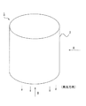
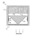
まず、本発明の実施の形態1に係る照明装置1の構成を説明する。図1は、照明装置1の外観を示す斜視図である。図2は、照明装置1の側面(図1に示すA方向)から見た平面図である。図3は、照明装置1の発光方向(図1に示すB方向)から見た平面図である(なお、説明のため保護用透光板51は取り外した状態としている)。図4は、図2におけるC1−C2面(筐体部2の中心軸に沿った面)における照明装置1の構造を示す断面図である。図5は、図2におけるD1−D2面における照明装置1の構造を示す断面図である。
First, the structure of the illuminating device 1 which concerns on Embodiment 1 of this invention is demonstrated. FIG. 1 is a perspective view showing an appearance of the lighting device 1. FIG. 2 is a plan view seen from the side surface (direction A shown in FIG. 1) of the lighting device 1. FIG. 3 is a plan view seen from the light emitting direction of the lighting device 1 (the B direction shown in FIG. 1) (for the sake of explanation, the protective
図1〜図5に示すように、照明装置1は、筐体部2と、保護用透光板51とを備える。また、その内部には、基板31(本発明の支持手段に相当する。)、固体発光素子32、電源ユニット52、配線ケーブル53、反射ユニット54(本発明の反射手段に相当する。)が具備されている。
As shown in FIGS. 1 to 5, the lighting device 1 includes a
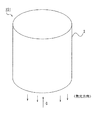
筐体部2は、本発明の筐体手段に相当し、通常放熱性を鑑み、熱伝導率が高い金属(好ましくは、熱伝導率が200[W/(m・K)以上]の金属)により構成される。例えば、筐体部2は、アルミニウムで構成される。筐体部2にアルミニウムを用いる理由としては、安価であること、成形が行いやすいこと、リサイクル性が良いこと、熱伝導率が200[W/(m・K)以上]以上であること、及び、放熱特性が高いことなどが挙げられる。さらに、アルミニウムで構成した筐体部2をアルマイト処理することも効果的である。筐体部2の表面積を拡大することができ、放熱性を高める効果がある。
The
なお、本実施の形態においては、筐体部2を円柱として構成しているが、これに限定されるものではない。三角柱や、四角柱などであって良く、必要に応じて任意に設定してよい。
In addition, in this Embodiment, although the housing | casing
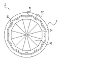
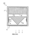
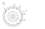
筐体部2は、中空部56(本発明の中空構造に相当する。)を備える。また、中空部56は一方向に開口部57を有する。図6は、筐体部2を開口部57方向から見た平面図である。図7は、筐体部2の中心軸に沿った面の構造を示す断面図である。
The housing | casing
図6及び図7に示すように、中空部56の内壁面は、法線が直角に筐体部2の中心軸(筐体部2の中心軸とは、筐体部2の中心を通る軸であり、本実施の形態では筐体部2を円柱として構成しているが、筐体部2の中心を通り前記円柱の高さ方向に沿った軸である。)へと向かう保持面41が複数備えられる。この保持面41は、固体発光素子32を保持する。具体的には、固体発光素子32が実装される基板31が密着配置される(すなわち、基板31を介し、固体発光素子32を保持する。)。
As shown in FIGS. 6 and 7, the inner wall surface of the
保持面41は、筐体部2の中心軸の周方向に正多角形柱空間を形成するように(正多角形柱空間の側面となるように)配置される(なお、本実施の形態においては正12角形柱として表しているが、これに限定されない。正3角形柱、正4角形柱等であってもよい)。
The holding
このように保持面41を配置する理由であるが、部品点数を減らしコストを削減するためである。照明装置1に使用する基板31は柔軟性を有するものであって、正多角形柱空間の側面を形成する全ての保持面41に対し、容易に密着配置することができる。すなわち、正多角形柱空間の側面(複数の保持面41)に沿って、基板31は配置され、故に1個体のみの基板31により照明装置1を構成することも可能となる。このことは、コスト削減へとつながる。
The reason for arranging the holding
また、照明装置1は、従来品にかわる照明装置である。そのため、照明装置1には、明るさが従来品と同等以上であり、また大きさについては従来品と同等であることが求められる。 Moreover, the illuminating device 1 is an illuminating device which replaces a conventional product. For this reason, the lighting device 1 is required to have a brightness that is equal to or higher than that of the conventional product and that is equal in size to the conventional product.
まず、明るさについてであるが、固体発光素子32としてハイパワーLEDを採用する。この際多数個のハイパワーLEDを使用する必要がある。照明装置1は、多数個のハイパワーLEDを具備しており、故に明るさの要求を満たすことが可能である。
First, regarding brightness, a high power LED is employed as the solid state
ただし、上記のように多数個のハイパワーLEDを採用することで、照明装置の大きさが大きくなっては、大きさに対する要求を満たすことができない。そこで、照明装置1では、中空部56の側面である保持面41が固体発光素子32(ハイパワーLED)を保持する。
However, by adopting a large number of high power LEDs as described above, if the size of the lighting device is increased, the demand for the size cannot be satisfied. Therefore, in the lighting device 1, the holding
ここで、保持面41の総和の面積は、筐体部2の底面43の面積より広くすることが容易にできる。よって、照明装置1は、筐体部2を大きくすることなく、コンパクトに多数個の固体発光素子32(ハイパワーLED)を配置することができる。そのため、上記大きさの要求にもこたえることができる。
Here, the total area of the holding surfaces 41 can be easily made larger than the area of the
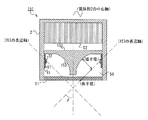
基板31は、本発明の支持手段に相当し、筐体部2の有する中空部56の内側に配置される。図8は、基板31の構成を示す図である。基板31は、略長方形状である。図8は、その一例であって、ベース部61、絶縁層62及び配線層63により構成され、平面状の基板である。なお、配線層63の絶縁層62と逆側の表面には、素子取り付け用パッド66、配線用パッド67を除く部分にレジスト膜が構成されている。
The board |
ここで、ベース部61は、柔軟性を有する金属板である。具体的には、ステンレス等の金属である。厚みは、柔軟性を確保できる範囲で任意であってよいが、発明者らの試験によれば、厚さ0.2[mm]が最適であった。 Here, the base portion 61 is a flexible metal plate. Specifically, it is a metal such as stainless steel. The thickness may be arbitrary as long as flexibility can be ensured, but according to the test conducted by the inventors, the thickness of 0.2 [mm] was optimum.
絶縁層62も、柔軟性を有し、十分な絶縁耐圧(電気的絶縁性)を備える絶縁層である。ここで、柔軟性を有する絶縁層としては、従来ポリイミド等が用いられてきた。しかしながら、このポリイミドの熱伝導率は、0.2[W/(m・K)]程度である。この値は非常に小さい値であり、固体発光素子32としてハイパワーLEDを使用する場合、その実装基板として用いることは適切ではない。ハイパワーLEDから発生した熱の放熱を行うことが困難となり、ハイパワーLEDの故障へとつながる可能性が危惧される。
The insulating
発明者らが採用した絶縁層62は、このポリイミドより高い熱伝導率を有するものであり、少なくとも1[W/(m・K)]以上の熱伝導率を有するものを採用した。この絶縁層62には、熱伝導率を高めるためフィラーが添加されている。さらには、柔軟性、絶縁耐圧共に実用に耐えうる性能を有することを確認している。
The insulating
配線層63は、銅などの金属からなり、配線及び素子取り付け用パッド66及び配線用パッド67が形成される層である。配線層63の厚みは任意であってよいが、数十〜数百[μm]であることが望ましい。このことにより、基板31の柔軟性を阻害することは発生しない。以上より、柔軟性を有し、かつ熱伝導率の高い基板31を構成することができる。
The
ここで、基板31には貫通孔であり、軸Eに沿った切りかき部65が設けられている。なお、軸Eとは、基板31の短辺方向に平行な任意の軸である。ただし、軸E上には固体発光素子32は存在しない。
Here, the
この切りかき部65は、基板31の曲げ部となる部分である。基板31は、放熱性を高めるためベース部61に金属を用いており、発明者らは、柔軟性に富んだ金属であるステンレス(厚さ0.2[mm])を採用している。
The
ただし、ステンレスは、ばね性が強く、所望の位置で曲げることが難しい。そのため、発明者らは、切りかき部65を設けることで、基板31においても所望の位置で曲げが行えるように工夫した。すなわち、切りかき部65が存在することにより、基板31を所望の位置、かつ基板31の短辺方向に平行に曲げることができる。
However, stainless steel has strong spring properties and is difficult to bend at a desired position. For this reason, the inventors have devised that the
所望の位置で、かつ基板31の短辺方向に平行に、基板31の曲げを行うことは、後述する基板31と、筐体部2とを密着させることと密接に関連するため重要である。
Bending the
なお、切りかき部65は、図5で示すように隣り合う保持面41の境界位置42上に配置できることを条件に、任意に形状、及び個数を設定してよい。
In addition, as long as the
ただし、全ての保持面41に同一個数の固体発光素子32が保持できるように設定することが肝要である(本実施の形態においては、全ての保持面41に固体発光素子32が1個保持されるとしているが、1個に限定されるものではない。2個以上であっても良い。)。もし、各保持面41に保持される固体発光素子32の個数が同一でないならば(すなわち、バラバラの個数であれば)、照明装置1の配光が筐体部2の中心軸に対する周方向に不均一となるためである。
However, it is important to set so that the same number of solid
また、ここで使用した固体発光素子32は、アノード電極とカソード電極とを有しセラミック又は樹脂等の筐体にベアチップ半導体がパッケージされたパッケージ品である。基板31の短辺方向と平行な所定の軸である軸F上(ただし、軸Fは軸E上には設けられない。)に、素子取り付け用パッド66としてアノードパッド部66a及びカソードパッド部66bを設けて、それらに半田付け等によりアノード電極及びカソード電極を夫々実装することが望ましい。
The solid state light emitting
ここで、基板31の短辺方向と平行な軸F上に、アノードパッド部66a及びカソードパッド部66bを設ける理由であるが、基板31は切りかき部65で曲げを行う。この曲げを行う軸Eは、前述のように基板31の短辺方向と平行な軸である。
Here, the reason is that the
この際、アノードパッド部66a及びカソードパッド部66bも基板31の短辺方向と平行な軸F上に設けられているため、基板31を曲げる際に、アノードパッド部66a及びカソードパッド部66bへの固体発光素子32のアノード電極、カソード電極の実装に伴い形成される半田付け部(不図示)に、負荷がかかることを防ぐことが可能となる。
At this time, since the
仮に、半田付け部(不図示)に負荷がかかった場合、半田クラック等の発生が危惧される。そのため、発明者らはアノードパッド部66a及びカソードパッド部66bを、基板31の短辺方向と平行な軸F上に設けることで、アノードパッド部66a及びカソードパッド部66bにおける半田付け部(不図示)に負荷がかかることを防いだ。
If a load is applied to a soldering part (not shown), the occurrence of solder cracks or the like is a concern. Therefore, the inventors provide the
配線用パッド67は、固体発光素子32に給電する電源ユニット52からの電気配線である配線ケーブル53が、電気的に接続される。この際の接続は、以下の通りの構造を有する。
The
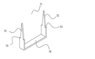
配線用パッド67には、中継部品71が実装される。この中継部品71とは、図9に示す構成を有する。図9は中継部品71の外観を示す斜視図である。
A
中継部品71は、図9に示す通り側面から見た形状が略コの字形状である。すなわち、中継部品71は、配線用パッド67に接続される平面状の第1部材74と、第1部材74の配線用パッド67に接続される面と反対の面の、第1部材74の長手方向の両端に、第1部材74と垂直に接続される2つの尖塔部72とを備える。
As shown in FIG. 9, the
ここで、中継部品71の形状は、コの字形状に限定されるものではなくL字形状であってもよい。すなわち、中継部品71は、配線用パッド67に接続される平面状の第1部材74と、第1部材74の配線用パッド67に接続される面と反対の面の、第1部材74の長手方向の一端に、第1部材74と垂直に接続される1つの尖塔部72とを備えてもよい。しかしながら、基板31への実装の利便性を考えればコの字形状であることが望ましい。
Here, the shape of the
その理由は、次に示す通りである。基板31への中継部品71の実装を行う際には、自動実装装置を用いて行うことが照明装置1を量産する上で効率的である。このとき、中継部品71をエンボステーピング化し、基板31に自動的に配置する。
The reason is as follows. When the
その際、中継部品71がもし、L字形状であれば、基板31の自動配置時に中継部品71のバランスが崩れ、所望の位置に配置することが難しくなる。一方、コの字形状であれば、中継部品71のバランスの崩れが発生せず、基板31の自動配置を所望の位置に行うことができる。
At this time, if the
また、中継部品71は導電性を有する材質で構成される。また、図10に示すように中継部品71は、半田付けにより基板31の配線用パッド67に実装される。さらには、尖塔部72は半田付けにより配線ケーブル53のラグ端子68と接続される。そのため、中継部品71には、半田付けに耐えうる耐熱性を有する材質を選択する必要がある。通常、中継部品71は、アルミニウム又は銅等の金属により構成される。
The
また、中継部品71は、リフロー半田法により配線用パッド67に実装されることが望ましい。これにより、簡便かつ確実に、中継部品71を配線用パッド67に実装できる。
The
また、中継部品71の尖塔部72には、所定の段73が設けられることが望ましい。このようにすることにより、配線ケーブル53の絶縁層が取り除かれた端部に半田付け、又はカシメ止めにより装着されたラグ端子68を、中継部品71の尖塔部72に挿入した状態において両者を半田付けにより接合する際の半田形状が、ラグ端子68上下から挟み込むようになり、より確実に接合することが可能となる。なお、中継部品71の尖塔部72に挿入した状態において両者接合する際の半田付けは、半田ごてを利用した手半田であってもよい。
In addition, it is desirable that a
ここで、従来、基板31に配線ケーブル53を電気的に接続する際には、配線ケーブル53の端部を、配線用パッド67にスポット半田法(半田ごてを利用した手半田など)により接続していた。
Here, conventionally, when the
しかしながら、この方法では、半田付けのみにより配線用パッド67と配線ケーブル53とが接続されているため、接続の強度が十分ではない。よって、万が一の大地震の発生などに伴う振動により、配線用パッド67から配線ケーブル53が外れる可能性がある。特に、基板31は金属基板であり、金属基板の熱伝導性が高いので、配線用パッド67の温度を所望の温度に上昇させることが難しい。そのため、半田付け不良により、配線用パッド67から配線ケーブル53が外れるリスクが高まってしまう。
However, in this method, since the
この対策としては、基板31に配線用スルーホール部(不図示)を設けることも考えられる。このようにすれば、確かに配線ケーブル53が、配線用スルーホール部(不図示)から外れるリスクを低減することができる。
As a countermeasure, it is conceivable to provide a wiring through-hole portion (not shown) in the
しかしながら、基板31は金属基板であるため、余分な部分まで電気的に接続されてしまい、電気的な短絡を発生してしまうなどの問題がある。したがって、スルーホール部(不図示)を設けることは容易ではない。
However, since the
また、リフロー法を用いて基板31に取り付けることができるコネクタ端子が開発されているが、このようなコネクタ端子は、概してその体積が大きい。そのため、基板31に実装される固体発光素子32からの発光をコネクタ端子が遮ってしまうという問題がある。
Moreover, although the connector terminal which can be attached to the board |
それに対し、照明装置1に採用した中継部品71は非常にコンパクトであり、そのような問題が発生しない。故にそのメリットは大きい。
On the other hand, the
ここで、基板31は、筐体部2(保持面41)とは密着させることが必要である。これは、固体発光素子32で発生した熱を、基板31を介して、筐体部2に伝熱し、その表面より、大気中へ放熱するためである。
Here, the
もし、基板31と、筐体部2(保持面41)の密着性が低いのであれば、その間に空気が入り込んでしまう。空気の熱伝導率は低いため、基板31から筐体部2への伝熱性が低下する。このことを避けるため、基板31と筐体部2(保持面41)との間に、両面テープ(不図示)などを挟みこみ、密着性を高めることが望ましい。
If the adhesion between the
なお、両面テープを使用する場合には、基材を含まないものを選択することが肝要である。それは、基材は熱伝導率が低いので、基板31から筐体部2への熱伝導が阻害されるためである。
When using a double-sided tape, it is important to select one that does not contain a substrate. This is because the heat conductivity from the
また、保持面41は、平面であることが必要である。もし保持面41が曲面として構成されたのであれば、基板31と筐体部2(保持面41)とを密着することが不可能となる。これは、基板31上には、前述のごとく固体発光素子32が、アノードパッド部66a及びカソードパッド部66bに半田付けされることにより実装されている。この半田付け部(不図示)には、柔軟性がないため曲げることが不可能であり、よって、その部分を曲面に密着させることは不可能である。以上より、保持面41は平面であることが必要である。
Further, the holding
また、隣り合う保持面41の境界位置42に切りかき部65が位置するよう、基板31を配置することが必要である。切りかき部65は、上記のように基板31の曲げを行う位置である。したがって、隣り合う保持面41の境界位置42と、基板31の曲げ位置とが一致することとなる。このようにすることは、基板31と、保持面41との密着性を高めることにつながる。
Further, it is necessary to arrange the
もし、隣り合う保持面41の境界位置42と、基板31の曲げ位置とにずれがあると、基板31の曲げ位置が保持面41上に干渉してしまう。このことは、基板31と保持面41との密着性を阻害する要因となる。よって、隣り合う保持面41の境界位置42上に切りかき部65が位置するように基板31を配置することは肝要なことである。
If there is a deviation between the boundary position 42 between the adjacent holding surfaces 41 and the bending position of the
以上のように、基板31は、筐体部2の中空部56の内壁面であり、筐体部2の中心軸の周方向に正多角形柱空間(ここでは、正12角形柱)を形成する保持面41上に密着配置される。このような構成をとるため、照明装置1は、多数個の固体発光素子32を実装した平面状である基板31を用いて構成することができる。
As described above, the
固体発光素子32は、基板31に配置される。固体発光素子32は、例えば、LEDである。固体発光素子32は、1個当たりの消費電力が1W以上のいわゆるハイパワーLEDであり、表面実装型のLEDである。ハイパワーLEDは、光度が高く照明装置用途に好適である。照明装置1を一般的な照明として使用する場合、使用する固体発光素子32の発光色は、昼光色、昼白色、白色、温白色又は電球色に相当する色などが好適である。具体的には、例えば、複数の固体発光素子32は、JISZ9112「蛍光ランプの光源色及び演色性による区分」の4.2「色度範囲」に規定された昼光色、昼白色、白色、温白色又は電球色に相当する光を発光する。
The solid
また、複数の固体発光素子32は、ピーク波長が380〜500nmの光である青色を発光してもよい。青色は、精神的興奮を抑える効果があるといわれている。そのため、青色を発光する照明装置1は、防犯灯として好適である。
The plurality of solid state light emitting
ところで、固体発光素子32に使用されるハイパワーLEDは、消費電力が大きく、その分、熱として放出されるエネルギーも大きい。そのため、この熱が、ハイパワーLEDの近傍に蓄積すると、光度低下や、寿命特性の劣化等を招く。したがって、この熱を適切に処理することが肝要である。
By the way, the high power LED used for the solid state light emitting
そこで、固体発光素子32に使用されるハイパワーLEDは、表面実装型のLEDである。表面実装型のLEDを使用する理由としては、LED自身の電極面積が大きく、故に基板31に接触する面積が大きくなる。すなわち、表面実装型のLEDでは、発生した熱を効率的に基板31に熱伝導することができる。
Therefore, the high power LED used for the solid state light emitting
また、基板31は、上記のように熱伝導性の高い金属基板であり、筐体部2(保持面41)に密着して構成されている。また、筐体部2も熱伝導が高く、放熱性も高い金属(発明者らはアルミニウムを採用している)により構成されている。故に、照明装置1においては、固体発光素子32において発生した熱を適切に放熱することが可能である。
Moreover, the board |
保護用透光板51は、本発明の保護板に相当し、固体発光素子32などを保護するものであって、筐体部2の中空部56が有する開口部57に取り付けられている。透光性を有し、照明装置1の発光方向に配置される。保護用透光板51は、例えば平板状に形成される。保護用透光板51は、透明なガラス、アクリル樹脂又はポリカーボネート等により形成される。
The protective
また、保護用透光板51の表面又は/及び裏面には、表面処理により、微細な凹凸を不均一に形成してもよい。この表面処理は、例えば、サンドブラスト法を適用することにより容易に行うことができる。このことにより、固体発光素子32から発せられた光を拡散する(本発明の拡散手段に相当する。)。固体発光素子32から発せられた光は、指向性が強いので、局所的に照射される傾向にある。固体発光素子32から発せられた光を表面処理された保護用透光板51により拡散することによって、光の指向性を弱め、広い面積に均一に光を照射することができる。これは、特に照明装置1をダウンライトとして使用する場合に有効である。
In addition, fine irregularities may be formed unevenly on the front surface and / or back surface of the protective
なお、保護用透光板51は、その構成材料に拡散剤を添加することにより、固体発光素子32から発せられた光を拡散しても良い。さらに、この拡散剤を添加し構成した後、その表面又は/及び裏面に表面処理を行い、微細な凹凸を不均一に形成することで、拡散効果を高めても良い。
The protective
電源ユニット52は、商用電源(不図示)から供給を受けた交流を直流化し、固体発光素子32に電源供給を行う。この電源ユニット52は、長寿命なものであることが望ましい。これは、固体発光素子32をハイパワーLEDとした場合において、ハイパワーLEDは非常に長寿命である。したがって、それと同程度の寿命を有する電源ユニット52を採用することが好ましい。
The
またこの場合において、ハイパワーLED(固体発光素子32)に供給する電力を任意に制御可能なものであることも好ましい。ハイパワーLEDは、供給する電力を制御することにより自在に調光することが可能であるためである。ハイパワーLEDを調光することにより、必要な明るさを自在に設定することができ照明装置1の利用者の利便性を向上することが可能となる。 In this case, it is also preferable that the power supplied to the high power LED (solid light emitting element 32) can be arbitrarily controlled. This is because the high power LED can be dimmed freely by controlling the power supplied. By dimming the high-power LED, the necessary brightness can be set freely, and the convenience of the user of the lighting device 1 can be improved.
配線ケーブル53は、電源ユニット52と基板31とを電気的に接続する電気ケーブルである。電源ユニット52において生成した直流を、基板31に設けられた配線用パッド67へと配電する。これにより、固体発光素子32へ直流が供給される。なお、配線ケーブル53と、配線用パッド67との接続は、中継部品71を介して接続される。
The
反射ユニット54は、本発明の反射手段に相当し、筐体部2が有する中空部56の内部に配置される。
The
反射ユニット54には、反射面55が複数備えられている。図中に示すように、反射面55が保持面41に1対1に対向して配置されるように構成することが好ましい。ここで1つの反射面55に対し、複数の保持面41が対向するように設定されても良いが、固体発光素子32から発せられた光を開口部57に効率よく導くためには、反射面55が保持面41に1対1に対向して配置されるように構成することが好ましい。
The
反射面55は対向する保持面41上に配置されている固体発光素子32から発せられる光を反射して、筐体部2の開口部57に備えられる保護用透光板51を介し、照明装置1の外部へと光を導く役割を担う。図11は、図4と同様、筐体部2の中心軸に沿った面における照明装置1の構造を示す断面図であり、照明装置1において固体発光素子32から発せられた光の軌跡を示すものである。
The reflecting
このように、照明装置1においては、固体発光素子32から発せられた光を反射面55にて開口部57方向へ向け反射する。この光は、保護用透光板51を介し照明装置1の外部へと導かれ、照明に供される。
Thus, in the illuminating device 1, the light emitted from the solid
ここで、反射面55の表面の傾斜に沿った軸である表面軸が筐体部2の中心軸に対してなす角度αは、任意であってよいが、適切に固体発光素子32から発せられる光を反射して、筐体部2の開口部57に備えられる保護用透光板51を介し、照明装置1の外部へと光を導くことができる角度であることが肝要である。
Here, an angle α formed by the surface axis, which is an axis along the inclination of the surface of the reflecting
角度αは、筐体部2の大きさなどに応じて決定してよいが、発明者らの試作によれば、概ね40度から50度の範囲であれば良好な結果が得られている。
Although the angle α may be determined according to the size of the
ここで、特許文献1に開示されるLED照明器具においては、図22に示すように下面に開口部が設けられた筐体1310と、周部に比べて中央部が凹んだドーム状であって、中央部を上側にして筐体1310内に収納された凹面鏡1314と、凹面鏡1314の周部に沿って、発光面を凹面鏡1314の中央部側にしてLED1302が複数配置される。その上でLED1302からの光を、凹面鏡1314で反射することによって、筐体1310の開口部を通して照明を行うとされている。
Here, in the LED lighting apparatus disclosed in Patent Document 1, as shown in FIG. 22, a
しかしながら、特許文献1に開示されるLED照明器具は、以下の点で問題点があると考えられる。それは、特許文献1には明示されていないが、LED1302は基板上に実装し、その上でLED照明器具に配置することが一般的である。この際、平面状の基板に複数のLED1302を実装し、その上でLED照明器具に配置することが望ましい。このようにすることにより、製造に係るコストの削減を図ること等のメリットがある。しかしながら、特許文献1に開示されるLED照明装置においては、図22に記載されている通り、LED1302はキャップ部1312に取り付けられているものの、円周に沿って、発光面を凹面鏡1314の中央部側にして配置されている。したがって、LED1302を立体的に配置することが必要になる。
However, the LED lighting apparatus disclosed in Patent Document 1 is considered problematic in the following respects. Although it is not explicitly described in Patent Document 1, it is general that the
そのため、上記のように平面状の基板に複数のLED1302を実装し、その上でLED照明器具内に配置することは困難であると考えられる。したがって、個々のLED1302毎に別の個体の基板に実装することが必要であると推定される。このことは、製造に係るコストの増大に直接的につながる。
For this reason, it is considered difficult to mount a plurality of
一方、照明装置1は、保持面41が筐体部2の中心軸の周方向に正多角形柱空間を形成するように(正多角形柱空間の側面となるように)配置される。また、照明装置1に使用する基板31は柔軟性を有するものであって、正多角形柱空間の側面を形成する全ての保持面41に対し、容易に密着配置することができる。すなわち、正多角形柱空間の側面(複数の保持面41)に沿って、基板31は配置され、故に1個体のみの基板31により照明装置1を構成することも可能となる。このことは、コスト削減へとつながる。
On the other hand, the illuminating device 1 is arrange | positioned so that the holding
また、照明装置1は、従来品(従来ランプ類を用いて構成されていたダウンライト、スポットライト)にかわる照明装置である。そのため、照明装置1には、明るさが従来品と同等以上であり、また大きさについては従来品と同等であることが求められる。 Moreover, the illuminating device 1 is an illuminating device which replaces conventional products (downlights and spotlights configured using conventional lamps). For this reason, the lighting device 1 is required to have a brightness that is equal to or higher than that of the conventional product and that is equal in size to the conventional product.
まず、明るさについてであるが、固体発光素子32としてハイパワーLEDを採用する。この際多数個のハイパワーLEDを使用する必要がある。照明装置1は、多数個のハイパワーLEDを具備しており、故に明るさの要求を満たすことが可能である。
First, regarding brightness, a high power LED is employed as the solid state
ただし、上記のように多数個のハイパワーLEDを採用することで、照明装置の大きさが大きくなっては、大きさに対する要求を満たすことができない。そこで、照明装置1では、中空部56の側面である保持面41が固体発光素子32(ハイパワーLED)を保持する。
However, by adopting a large number of high power LEDs as described above, if the size of the lighting device is increased, the demand for the size cannot be satisfied. Therefore, in the lighting device 1, the holding
ここで、保持面41の総和の面積は、筐体部2の底面43の面積より広くすることが容易にできる。よって、照明装置1は、筐体部2を大きくすることなく、コンパクトに多数個の固体発光素子32(ハイパワーLED)を配置することができる。そのため、上記大きさの要求にもこたえることができる。
Here, the total area of the holding surfaces 41 can be easily made larger than the area of the
(変形例1)
本発明の実施の形態1の変形例1に係る照明装置121が、照明装置1と異なる点は、反射ユニット54が反射ユニット122に変更されるのみである。よって、そのほかの構成要素については、同一の符号を付し、説明を省略する。
(Modification 1)
The
図12は、照明装置121の筐体部2の中心軸に沿った面の構造を示す断面図である。反射ユニット122には、反射ユニット54と同様に保持面41に対向するよう反射面123を備える。この反射面123には微細なディンプル形状(球面状のへこみ)が備えられる。
FIG. 12 is a cross-sectional view illustrating a structure of a surface along the central axis of the
反射面123にこのような形状を設ける理由であるが、固体発光素子32から発せられる光を拡散するためである。光の指向性を緩和する目的で設けられる。
The reason for providing such a shape on the reflecting
(変形例2)
本発明の実施の形態1の変形例2に係る照明装置131が照明装置1と異なる点は、反射ユニット54が反射ユニット132に変更されるのみである。よって、そのほかの構成要素については、同一の符号を付し、説明を省略する。
(Modification 2)
The
図13は、照明装置131の筐体部2の中心軸に沿った面の構造を示す断面図である。反射ユニット132には、反射ユニット54と同様に保持面41に対向するよう反射面133を備える。この反射面133には微細な凹凸形状が備えられる。
FIG. 13 is a cross-sectional view illustrating a structure of a surface along the central axis of the
反射面133にこのような形状を設ける理由であるが、実施の形態1の変形例1に示す照明装置121の反射面123と同様、固体発光素子32から発せられる光を拡散するためである。光の指向性を緩和する目的で設けられる。
The reason for providing such a shape on the reflecting
(変形例3)
本発明の実施の形態1の変形例3に係る照明装置141が照明装置1と異なる点は、反射ユニット54が反射ユニット142に変更されるのみである。よって、そのほかの構成要素については、同一の符号を付し、説明を省略する。
(Modification 3)
The
図14は、照明装置141の発光方向から見た平面図である。ここでは説明のため、保護用透光板51を取り外した状態で示している。
FIG. 14 is a plan view seen from the light emitting direction of the
反射ユニット142は、反射ユニット54と同様に保持面41に対向するよう反射面143を備える。この反射面143には、筐体部2の中心軸の周方向に凹面が設けられる。凹面が設けられることにより、固体発光素子32から発せられた光は凹面の焦点に集光されるが、焦点通過後は筐体部2の中心軸の周方向に発散される(焦点通過後の光が照明に供される)。
Similar to the
このことにより、照明装置141は、筐体部2の中心軸の周方向の光の均一性を向上することができる。
Thereby, the illuminating
なお、上記においては筐体部2の中心軸の周方向に凹面を設けるとしたが、凸面であっても良い。この場合においてもほぼ同様の効果が得られる。
In the above description, the concave surface is provided in the circumferential direction of the central axis of the
また、反射面143の表面に、ディンプル形状、又は凹凸形状を備えてもよい。
The surface of the reflecting
(実施の形態2)
本発明の実施の形態2に係る照明装置151は、反射面153が楕円弧形状となっている。楕円弧形状の楕円率を任意に設定することにより所望の配光特性が得られるという特徴を有している。
(Embodiment 2)
In the
本発明の実施の形態2にかかる照明装置151が、照明装置1と異なる点は、反射ユニット152のみである。そのほかの構成については、同一の符号を付し、説明を省略する。
The
図15は、照明装置151の外観を示す斜視図であり、図16は、照明装置151を図15のG方向(発光方向側)から見た平面図である(説明のため、保護用透光板51は取り外された状態を示している)。図17A及び図17Bは、筐体部2の中心軸に沿った面における構造を示す断面図である。
FIG. 15 is a perspective view showing the appearance of the
反射ユニット152は、反射ユニット54と同様、保持面41に対向するよう反射面153を備える。反射面153は、固体発光素子32を一方の焦点とし、その長辺軸と筐体部2の中心軸とのなす角βが、所定の範囲内である楕円弧形状となっている(図17A参照)。
Similar to the
長辺軸と筐体部2の中心軸とのなす角βは、筐体部2の形状等に基づき任意に設定してよいが、発明者らの試作においては、概ね40度〜50度の範囲であれば良好な結果が得られている。
The angle β formed by the long side axis and the central axis of the
ここで、照明装置151においては、反射面153の楕円率を設定することにより照明範囲(配光特性)を任意に設定することが可能であるという特徴を有している。なお、楕円率とは、楕円(楕円弧形状)の短半径と長半径との比である。このことを、反射ユニット152にかわり、反射面153―1を有する反射ユニット152―1を使用した照明装置151―1と比較することにより説明する。図18A及び図18Bは、照明装置151―1における筐体部2の中心に沿った面における構造を示す断面図である。
Here, the
反射面153と、反射面153―1との相違点であるが、楕円率が異なる点である。反射面153の楕円率は、反射面153―1の楕円率と比較して大きな値となっている。
The difference between the reflecting
この場合において、図17B、及び図18Bに示す光の軌跡の通り、固体発光素子32から発せられ、反射面153により反射された光は、反射面153―1に反射された光と比べより広い範囲に向け届けられる。すなわち、照明範囲が広くなる。
In this case, the light emitted from the solid state light emitting
したがって、照明装置151においては、反射面153の楕円率を所望の照明範囲(配光特性)に応じて設定する。このことにより、容易に所望の照明範囲(配光特性)を得ることができる。
Therefore, in the
ただし、この際、楕円(楕円弧形状)の一方の焦点を固体発光素子32としているが、他方の焦点154(154―1)の位置を、開口部57付近、又は開口部57の外側(照明装置1の外部かつ発光方向側)に設定することが必要である。すなわち、焦点154(154―1)の位置が、開口部57付近、又は開口部57の外側となるよう楕円率を設定する必要がある。
However, at this time, one focus of the ellipse (elliptical arc shape) is the solid
この理由であるが、固体発光素子32より発せられ、焦点154(154―1)に集光された光は、図17B、及び図18Bに示す光の軌跡の通り、焦点154(154―1)通過後において再び広がる(発散する)。そのため、もし焦点154(154―1)を、中空部56内部に設定した場合、焦点154(154―1)に集光された光が中空部56内部で再び広がってしまい、反射面153(153―1)以外の部分(保持面41等)に当該光が接触することになる。このことは、所望の照明範囲(配光特性)を得られない原因となり、また固体発光素子32により発せられた光のロスへとつながってしまうためである。
For this reason, the light emitted from the solid-state
なお、反射面153に、ディンプル形状又は凹凸形状を設けることで固体発光素子32から発せられる光を拡散しても良い。また、反射面153の筐体部2の中心軸の周方向に凹面、又は凸面を設けることにより、筐体部2の中心軸の周方向の光の均一性を向上しても良い。
Note that light emitted from the solid state light emitting
(実施の形態3)
本発明の実施の形態3に係る照明装置211は、ベアチップ半導体213から発せられる光を利用した照明装置である。ベアチップ半導体213は、稠密に配置することができるという特徴を有している。そのため各保持面41に発光色の異なるベアチップ半導体213を複数稠密に備え、これらを発光色毎に独立に発光制御することにより、所望の色調を得られるという特徴を有している。
(Embodiment 3)
The
本発明の実施の形態3にかかる照明装置211が、照明装置1と異なる点は、基板31が基板212に変更される点と、固体発光素子32がベアチップ半導体213に変更される点のみである。そのほかの構成については、同一の符号を付し、説明を省略する。
The
図19は、照明装置211の外観を示す斜視図であり、図20は、照明装置211を図19のH方向(発光方向側)から見た平面図である(説明のため、保護用透光板51は取り外した状態を示している)。図21は、基板212の構成を示す図である。
19 is a perspective view showing the appearance of the
基板212の基板31との相違点は、配線層63が配線層231に変更される点のみである。その他の構成は基板31と同一であり、よって同一符号を付し説明を省略する。
The only difference between the
配線層231は、ベアチップ半導体213が配置できるよう実装パッド(不図示)が設けられ、実装パッド(不図示)上にベアチップ半導体213が実装されている。
The
ベアチップ半導体213は、各保持面41に対し同一個数(ここでは9個のベアチップ半導体213が備えられるとしたが、これに限定されない。)が配置できるよう基板212に配置される。
The
また、ベアチップ半導体213は、ハイパワーLEDにも使用されるLEDベアチップを採用している。このようなLEDベアチップは、光度の高い発光ができ、照明用途に適している。
Moreover, the
また、ベアチップ半導体213は、その組成により任意に発光色を設定できる。そのため、各保持面41に対し、同一の割合で発光色の異なる複数種類のベアチップ半導体213を配置し、種類毎に独立して発光制御(すなわち、種類毎に独立して供給する電力を設定)することも好ましい。
Further, the
例えば、3種類のベアチップ半導体213a、213b及び213cを3個ずつ各保持面41に配置できるように実装パッド(不図示)上に実装する。213aを青色発光、213bを赤色発光、213cを緑色発光とすることにより、照明装置211においては、任意の発光色を実現することが可能となる。
For example, three types of
このことは、照明装置211をシーン(時刻、季節等)に応じた発光色とすることができるということであり、その利用者に対し利便性を提供することへとつながる。
This means that the
なお、照明装置211において、反射ユニット54は、反射ユニット122、132、142及び152等に変更できることはいうまでもない。
Needless to say, in the
なお、本発明の照明装置1、121、131、141、151及び211は、上記実施の形態に限定されるものではなく、本発明の趣旨を逸脱しない範囲で自由に変形して実施することができる。
Note that the
例えば、固体発光素子32として、LEDを使用することを例示したが、ELを使用してもよい。ELもLED同様注目を集める新しい光源である。
For example, although the use of an LED has been exemplified as the solid
また、照明装置151において、その楕円弧形状の楕円率の異なる複数の反射領域を有する反射ユニット(反射面)を用いる。その上で、反射に供する反射領域を選択可能とすることで、配光特性を必要に応じて選択することができる照明装置151を実現することができる。
Moreover, in the illuminating
本発明は、照明装置に適用でき、特に、光源にLEDなどの固体発光素子を用いた照明装置に適用できる。 The present invention can be applied to an illuminating device, and particularly applicable to an illuminating device using a solid light emitting element such as an LED as a light source.
1、121、131、141、151、211 照明装置
2 筐体部
31、212 基板
32 固体発光素子
41 保持面
42 境界位置
43 底面
51 保護用透光板
52 電源ユニット
53 配線ケーブル
54、122、132、142、152 反射ユニット
55、123、133、143、153 反射面
56 中空部
57 開口部
61 ベース部
62 絶縁層
63、231 配線層
65 切りかき部
66 素子取り付け用パッド
66a アノードパッド部
66b カソードパッド部
67 配線用パッド
68 ラグ端子
71 中継部品
72 尖塔部
73 段
154 焦点
213、213a、213b、213c ベアチップ半導体
1302 LED
1310 筐体
1312 キャップ部
1314 凹面鏡
DESCRIPTION OF
1310
Claims (10)
前記複数の固体発光素子が配置される中空構造を有し、前記中空構造の一方向に開口部を有する筐体手段と、
所定の間隔の領域毎に前記複数の固体発光素子のいくつかが実装される支持手段と、
前記中空構造内に配置され、前記複数の固体発光素子が発する光を反射する反射手段と
を備え、
前記中空構造の一部の内壁面は、前記筐体手段の中心を通る軸である中心軸へと法線が直角に向かう平面からなり、前記支持手段を介して前記複数の固体発光素子を保持する保持面を複数構成し、
前記複数の保持面は、前記中心軸の周方向に正多角形柱空間を形成するよう配置され、
前記支持手段は、前記領域毎に前記保持面に密着するよう配置され、
前記反射手段は、前記固体発光素子が発した光を前記開口部に向け反射する
ことを特徴とする照明装置。 An illumination device that performs illumination using light emitted from a plurality of surface-mounted solid-state light emitting elements,
Housing means having a hollow structure in which the plurality of solid state light emitting elements are arranged, and having an opening in one direction of the hollow structure;
Support means on which some of the plurality of solid state light emitting elements are mounted for each of the predetermined distance areas;
A reflecting means disposed in the hollow structure and reflecting light emitted from the plurality of solid state light emitting elements;
Part of the inner wall surface of the hollow structure, wherein Ri Do from the normal line is directed at a right angle plane to the central axis is an axis passing through the center of the housing means, said plurality of solid state light emitting devices via said support means a holding surface for holding a plurality of configuration,
The plurality of holding surfaces are arranged to form a regular polygonal column space in a circumferential direction of the central axis,
The support means is arranged to be in close contact with the holding surface for each region,
The said reflection means reflects the light which the said solid light emitting element emitted toward the said opening part. The illuminating device characterized by the above-mentioned.
柔軟性を有する金属により構成されるベース部と、
1[W/(m・K)]以上の熱伝導率を有する電気的絶縁層と、
前記保持面のうち任意の2面の境界上に位置し、該支持手段の短辺方向に平行な任意の軸に沿った所定形状に貫通された切りかき部と
を備え、
前記筐体手段は、金属より構成され、
前記領域は、前記切りかき部を通る短辺方向の隣り合う軸間の領域であり、
前記支持手段は、前記中心軸の周方向に長辺が沿うように、前記切りかき部で曲げられて配置される
ことを特徴とする請求項1に記載の照明装置。 Said support means, Ri substantially rectangular der,
A base portion made of a flexible metal;
An electrically insulating layer having a thermal conductivity of 1 [W / (m · K)] or more;
A notch portion located on a boundary between any two surfaces of the holding surface and penetrating into a predetermined shape along an arbitrary axis parallel to the short side direction of the support means ,
The housing means is made of metal,
The region is a region between adjacent axes in the short side direction passing through the cut portion,
2. The lighting device according to claim 1 , wherein the support unit is arranged by being bent at the notch portion so that a long side extends along a circumferential direction of the central axis .
ことを特徴とする請求項1又は請求項2に記載の照明装置。 Said supporting means, the lighting device according to claim 1 or claim 2, characterized in that it is provided only one individual.
前記支持手段は、さらに、
前記アノード電極が接合されるパッドであるアノードパッド部と、
前記カソード電極が接合されるパッドであるカソードパッド部と
を備え、
前記アノードパッド部と前記カソードパッド部とは、該支持手段の短辺方向に平行な所定の軸上に位置する
ことを特徴とする請求項1〜3の何れか1項に記載の照明装置。 The solid state light emitting device is a packaged product having an anode electrode and a cathode electrode,
The support means further includes:
An anode pad portion which is a pad to which the anode electrode is bonded;
A cathode pad portion that is a pad to which the cathode electrode is bonded;
The lighting device according to any one of claims 1 to 3 , wherein the anode pad portion and the cathode pad portion are located on a predetermined axis parallel to a short side direction of the support means.
ことを特徴とする請求項1〜4の何れか1項に記載の照明装置。 All the said holding surfaces hold | maintain the same number of said solid light emitting elements. The illuminating device of any one of Claims 1-4 characterized by the above-mentioned.
を備える
ことを特徴とする請求項1〜5の何れか1項に記載の照明装置。 It said reflecting means, the lighting device according to any one of claim 1 to 5, characterized in that a reflective surface facing to the holding surface for each of the holding surface.
前記固体発光素子が発した光を拡散する拡散手段
を備える
ことを特徴とする請求項6に記載の照明装置。 The lighting device further includes:
The illuminating device according to claim 6 , further comprising a diffusing unit that diffuses light emitted from the solid state light emitting device.
ことを特徴とする請求項7に記載の照明装置。 The lighting device according to claim 7 , wherein the diffusing unit is provided on a surface of the reflecting surface and has a dimple shape or an uneven shape.
前記固体発光素子が該楕円弧形状の一方の焦点上に配置される
ことを特徴とする請求項6〜8の何れか1項に記載の照明装置。 In the cross section along the central axis, the reflecting surface has an elliptical arc shape;
The lighting device according to any one of claims 6 to 8 , wherein the solid-state light emitting element is disposed on one focal point of the elliptical arc shape.
前記楕円弧形状の他方の焦点は、前記開口部の付近又は前記開口部の外部に配置される
ことを特徴とする請求項9に記載の照明装置。 The angle formed by the central axis and the long-side axis of the elliptical arc shape is a value within a predetermined range,
The illumination device according to claim 9 , wherein the other focal point of the elliptical arc shape is disposed in the vicinity of the opening or outside the opening.
Priority Applications (1)
| Application Number | Priority Date | Filing Date | Title |
|---|---|---|---|
| JP2008008467A JP4124479B1 (en) | 2007-10-16 | 2008-01-17 | Lighting device |
Applications Claiming Priority (2)
| Application Number | Priority Date | Filing Date | Title |
|---|---|---|---|
| JP2007268590 | 2007-10-16 | ||
| JP2008008467A JP4124479B1 (en) | 2007-10-16 | 2008-01-17 | Lighting device |
Publications (2)
| Publication Number | Publication Date |
|---|---|
| JP4124479B1 true JP4124479B1 (en) | 2008-07-23 |
| JP2009117328A JP2009117328A (en) | 2009-05-28 |
Family
ID=39704921
Family Applications (2)
| Application Number | Title | Priority Date | Filing Date |
|---|---|---|---|
| JP2008008467A Expired - Fee Related JP4124479B1 (en) | 2007-10-16 | 2008-01-17 | Lighting device |
| JP2008231551A Pending JP2009117346A (en) | 2007-10-16 | 2008-09-09 | Illuminating device |
Family Applications After (1)
| Application Number | Title | Priority Date | Filing Date |
|---|---|---|---|
| JP2008231551A Pending JP2009117346A (en) | 2007-10-16 | 2008-09-09 | Illuminating device |
Country Status (1)
| Country | Link |
|---|---|
| JP (2) | JP4124479B1 (en) |
Cited By (3)
| Publication number | Priority date | Publication date | Assignee | Title |
|---|---|---|---|---|
| JP2010153285A (en) * | 2008-12-26 | 2010-07-08 | Iwasaki Electric Co Ltd | Led unit and illuminating device for odontotherapy |
| US20140126196A1 (en) * | 2012-11-08 | 2014-05-08 | Cree, Inc. | Integrated linear light engine |
| US8776382B2 (en) | 2008-10-02 | 2014-07-15 | Ihi Corporation | Cutting instrument |
Families Citing this family (80)
| Publication number | Priority date | Publication date | Assignee | Title |
|---|---|---|---|---|
| WO2011143643A2 (en) * | 2010-05-14 | 2011-11-17 | Matrix Railway Inc | Led lighting apparatus |
| US8807789B2 (en) | 2009-10-16 | 2014-08-19 | Dialight Corporation | LED illumination device for projecting light downward and to the side |
| US9412926B2 (en) | 2005-06-10 | 2016-08-09 | Cree, Inc. | High power solid-state lamp |
| JP5354191B2 (en) * | 2009-06-30 | 2013-11-27 | 東芝ライテック株式会社 | Light bulb shaped lamp and lighting equipment |
| DE102009042338B4 (en) * | 2009-09-21 | 2019-03-21 | Berchtold Holding Gmbh | surgical light |
| JP5327472B2 (en) * | 2009-09-25 | 2013-10-30 | 東芝ライテック株式会社 | Light bulb shaped lamp and lighting equipment |
| JP2011181254A (en) * | 2010-02-26 | 2011-09-15 | Jia-Ye Wu | Led lamp unit |
| US9024517B2 (en) | 2010-03-03 | 2015-05-05 | Cree, Inc. | LED lamp with remote phosphor and diffuser configuration utilizing red emitters |
| US10359151B2 (en) | 2010-03-03 | 2019-07-23 | Ideal Industries Lighting Llc | Solid state lamp with thermal spreading elements and light directing optics |
| US9316361B2 (en) | 2010-03-03 | 2016-04-19 | Cree, Inc. | LED lamp with remote phosphor and diffuser configuration |
| US8882284B2 (en) * | 2010-03-03 | 2014-11-11 | Cree, Inc. | LED lamp or bulb with remote phosphor and diffuser configuration with enhanced scattering properties |
| US9275979B2 (en) | 2010-03-03 | 2016-03-01 | Cree, Inc. | Enhanced color rendering index emitter through phosphor separation |
| US9310030B2 (en) | 2010-03-03 | 2016-04-12 | Cree, Inc. | Non-uniform diffuser to scatter light into uniform emission pattern |
| US8931933B2 (en) | 2010-03-03 | 2015-01-13 | Cree, Inc. | LED lamp with active cooling element |
| US8562161B2 (en) | 2010-03-03 | 2013-10-22 | Cree, Inc. | LED based pedestal-type lighting structure |
| US9057511B2 (en) | 2010-03-03 | 2015-06-16 | Cree, Inc. | High efficiency solid state lamp and bulb |
| US9625105B2 (en) | 2010-03-03 | 2017-04-18 | Cree, Inc. | LED lamp with active cooling element |
| US8632196B2 (en) | 2010-03-03 | 2014-01-21 | Cree, Inc. | LED lamp incorporating remote phosphor and diffuser with heat dissipation features |
| US9500325B2 (en) | 2010-03-03 | 2016-11-22 | Cree, Inc. | LED lamp incorporating remote phosphor with heat dissipation features |
| US9062830B2 (en) | 2010-03-03 | 2015-06-23 | Cree, Inc. | High efficiency solid state lamp and bulb |
| KR101090728B1 (en) | 2010-04-10 | 2011-12-08 | 엘지이노텍 주식회사 | Lighting apparatus |
| EP2789899B1 (en) * | 2010-04-10 | 2017-07-05 | LG Innotek Co., Ltd. | Lighting apparatus |
| US8596821B2 (en) | 2010-06-08 | 2013-12-03 | Cree, Inc. | LED light bulbs |
| JP5609332B2 (en) * | 2010-07-05 | 2014-10-22 | 住友ベークライト株式会社 | Light source device and lighting apparatus |
| US10451251B2 (en) | 2010-08-02 | 2019-10-22 | Ideal Industries Lighting, LLC | Solid state lamp with light directing optics and diffuser |
| JP5573468B2 (en) * | 2010-08-04 | 2014-08-20 | 住友ベークライト株式会社 | Light source device and lighting apparatus |
| JP5655423B2 (en) * | 2010-08-06 | 2015-01-21 | 住友ベークライト株式会社 | Light source device and lighting apparatus |
| TW201215811A (en) * | 2010-10-04 | 2012-04-16 | Light Engine Ltd | Flat module light source |
| EP2738445B1 (en) | 2010-11-08 | 2018-01-10 | LG Innotek Co., Ltd. | Lighting apparatus |
| US8587185B2 (en) | 2010-12-08 | 2013-11-19 | Cree, Inc. | Linear LED lamp |
| US9068701B2 (en) | 2012-01-26 | 2015-06-30 | Cree, Inc. | Lamp structure with remote LED light source |
| US9234655B2 (en) | 2011-02-07 | 2016-01-12 | Cree, Inc. | Lamp with remote LED light source and heat dissipating elements |
| US11251164B2 (en) | 2011-02-16 | 2022-02-15 | Creeled, Inc. | Multi-layer conversion material for down conversion in solid state lighting |
| US8704432B2 (en) * | 2011-05-25 | 2014-04-22 | Seoul Semiconductor Co., Ltd. | LED lamp |
| KR101863869B1 (en) * | 2011-06-29 | 2018-06-01 | 엘지이노텍 주식회사 | Lighting device |
| JP5807951B2 (en) * | 2011-07-15 | 2015-11-10 | Necライティング株式会社 | Organic EL lighting unit and organic EL lighting device |
| US9482421B2 (en) | 2011-12-30 | 2016-11-01 | Cree, Inc. | Lamp with LED array and thermal coupling medium |
| JP5935397B2 (en) * | 2012-03-05 | 2016-06-15 | 岩崎電気株式会社 | lighting equipment |
| US9488359B2 (en) | 2012-03-26 | 2016-11-08 | Cree, Inc. | Passive phase change radiators for LED lamps and fixtures |
| US8757839B2 (en) | 2012-04-13 | 2014-06-24 | Cree, Inc. | Gas cooled LED lamp |
| US9234638B2 (en) | 2012-04-13 | 2016-01-12 | Cree, Inc. | LED lamp with thermally conductive enclosure |
| US9410687B2 (en) | 2012-04-13 | 2016-08-09 | Cree, Inc. | LED lamp with filament style LED assembly |
| US9310065B2 (en) | 2012-04-13 | 2016-04-12 | Cree, Inc. | Gas cooled LED lamp |
| US9651240B2 (en) | 2013-11-14 | 2017-05-16 | Cree, Inc. | LED lamp |
| US9322543B2 (en) | 2012-04-13 | 2016-04-26 | Cree, Inc. | Gas cooled LED lamp with heat conductive submount |
| US9395051B2 (en) | 2012-04-13 | 2016-07-19 | Cree, Inc. | Gas cooled LED lamp |
| US9395074B2 (en) | 2012-04-13 | 2016-07-19 | Cree, Inc. | LED lamp with LED assembly on a heat sink tower |
| US9951909B2 (en) | 2012-04-13 | 2018-04-24 | Cree, Inc. | LED lamp |
| CN104488097B (en) * | 2012-07-19 | 2017-08-01 | 夏普株式会社 | Row light-emitting device and its manufacture method |
| DE102012109149A1 (en) * | 2012-09-27 | 2014-03-27 | Osram Opto Semiconductors Gmbh | Ring light module and method for producing a ring light module |
| DE102012109146A1 (en) * | 2012-09-27 | 2014-03-27 | Osram Opto Semiconductors Gmbh | Ring light module and method for producing a ring light module |
| US9664369B2 (en) | 2013-03-13 | 2017-05-30 | Cree, Inc. | LED lamp |
| WO2014155281A1 (en) * | 2013-03-26 | 2014-10-02 | Koninklijke Philips N.V. | Lighting device and luminaire |
| EP2979023B1 (en) | 2013-03-26 | 2017-02-22 | Philips Lighting Holding B.V. | Lighting device and luminaire |
| US9285082B2 (en) | 2013-03-28 | 2016-03-15 | Cree, Inc. | LED lamp with LED board heat sink |
| US9169977B2 (en) | 2013-06-28 | 2015-10-27 | Cree, Inc. | LED lamp |
| US9222659B2 (en) | 2013-06-28 | 2015-12-29 | Cree, Inc. | LED lamp |
| FR3015002B1 (en) * | 2013-12-17 | 2018-07-13 | Legrand France | LIGHTING DEVICE |
| US9726330B2 (en) | 2013-12-20 | 2017-08-08 | Cree, Inc. | LED lamp |
| US10030819B2 (en) | 2014-01-30 | 2018-07-24 | Cree, Inc. | LED lamp and heat sink |
| US9360188B2 (en) | 2014-02-20 | 2016-06-07 | Cree, Inc. | Remote phosphor element filled with transparent material and method for forming multisection optical elements |
| US9518704B2 (en) | 2014-02-25 | 2016-12-13 | Cree, Inc. | LED lamp with an interior electrical connection |
| US9759387B2 (en) | 2014-03-04 | 2017-09-12 | Cree, Inc. | Dual optical interface LED lamp |
| US9328876B2 (en) | 2014-03-19 | 2016-05-03 | Cree, Inc. | High efficiency LED lamp |
| US9388948B2 (en) | 2014-03-25 | 2016-07-12 | Cree, Inc. | LED lamp |
| US9765935B2 (en) | 2014-03-25 | 2017-09-19 | Cree, Inc. | LED lamp with LED board brace |
| US9328874B2 (en) | 2014-03-25 | 2016-05-03 | Cree, Inc. | LED lamp |
| US9927100B2 (en) | 2014-03-25 | 2018-03-27 | Cree, Inc. | LED lamp with LED board brace |
| US9562677B2 (en) | 2014-04-09 | 2017-02-07 | Cree, Inc. | LED lamp having at least two sectors |
| US9435528B2 (en) | 2014-04-16 | 2016-09-06 | Cree, Inc. | LED lamp with LED assembly retention member |
| US9488322B2 (en) | 2014-04-23 | 2016-11-08 | Cree, Inc. | LED lamp with LED board heat sink |
| US9618162B2 (en) | 2014-04-25 | 2017-04-11 | Cree, Inc. | LED lamp |
| US9951910B2 (en) | 2014-05-19 | 2018-04-24 | Cree, Inc. | LED lamp with base having a biased electrical interconnect |
| US9618163B2 (en) | 2014-06-17 | 2017-04-11 | Cree, Inc. | LED lamp with electronics board to submount connection |
| JP6137231B2 (en) * | 2015-04-08 | 2017-05-31 | 三菱電機株式会社 | lamp |
| JP6187527B2 (en) * | 2015-04-08 | 2017-08-30 | 三菱電機株式会社 | lamp |
| JP6717611B2 (en) * | 2016-02-19 | 2020-07-01 | ローム株式会社 | LED lighting device and inspection device |
| JP6789650B2 (en) * | 2016-03-28 | 2020-11-25 | シチズン時計株式会社 | LED light emitting device |
| US10260683B2 (en) | 2017-05-10 | 2019-04-16 | Cree, Inc. | Solid-state lamp with LED filaments having different CCT's |
| KR102228150B1 (en) * | 2020-07-31 | 2021-03-16 | 주식회사 락소 | Hidden line lighting molding for easy lighting embedding |
-
2008
- 2008-01-17 JP JP2008008467A patent/JP4124479B1/en not_active Expired - Fee Related
- 2008-09-09 JP JP2008231551A patent/JP2009117346A/en active Pending
Cited By (4)
| Publication number | Priority date | Publication date | Assignee | Title |
|---|---|---|---|---|
| US8776382B2 (en) | 2008-10-02 | 2014-07-15 | Ihi Corporation | Cutting instrument |
| JP2010153285A (en) * | 2008-12-26 | 2010-07-08 | Iwasaki Electric Co Ltd | Led unit and illuminating device for odontotherapy |
| US20140126196A1 (en) * | 2012-11-08 | 2014-05-08 | Cree, Inc. | Integrated linear light engine |
| US9482396B2 (en) * | 2012-11-08 | 2016-11-01 | Cree, Inc. | Integrated linear light engine |
Also Published As
| Publication number | Publication date |
|---|---|
| JP2009117328A (en) | 2009-05-28 |
| JP2009117346A (en) | 2009-05-28 |
Similar Documents
| Publication | Publication Date | Title |
|---|---|---|
| JP4124479B1 (en) | Lighting device | |
| US20210356083A1 (en) | Light bulb shaped lamp | |
| US8911108B2 (en) | Light bulb shaped lamp and lighting apparatus | |
| JP5333758B2 (en) | Lighting device and lighting fixture | |
| WO2010098349A1 (en) | Led lamp | |
| JP5545547B2 (en) | Light source body and lighting apparatus | |
| WO2011024861A1 (en) | Light-emitting device and illuminating device | |
| JP3163443U (en) | LED lighting device | |
| JP2010238972A (en) | Phosphor and luminaire | |
| JP2011216216A (en) | Light-emitting diode lighting apparatus | |
| JP2017054749A (en) | Light emitting device and light source for illumination | |
| JP2011181252A (en) | Lighting fixture | |
| JP5845053B2 (en) | LED lamp | |
| JP2015053233A (en) | Light source for illumination, and luminaire | |
| JP6920665B2 (en) | Lighting light source and lighting equipment | |
| WO2014041721A1 (en) | Light source for illumination and illumination device | |
| JP5617982B2 (en) | Lamp with lamp and lighting equipment | |
| JP5574204B2 (en) | Lighting device and lighting fixture | |
| JP2011233443A (en) | Light-emitting diode lighting system |
Legal Events
| Date | Code | Title | Description |
|---|---|---|---|
| TRDD | Decision of grant or rejection written | ||
| A01 | Written decision to grant a patent or to grant a registration (utility model) |
Free format text: JAPANESE INTERMEDIATE CODE: A01 Effective date: 20080430 |
|
| A01 | Written decision to grant a patent or to grant a registration (utility model) |
Free format text: JAPANESE INTERMEDIATE CODE: A01 |
|
| A61 | First payment of annual fees (during grant procedure) |
Free format text: JAPANESE INTERMEDIATE CODE: A61 Effective date: 20080501 |
|
| R150 | Certificate of patent or registration of utility model |
Free format text: JAPANESE INTERMEDIATE CODE: R150 |
|
| FPAY | Renewal fee payment (event date is renewal date of database) |
Free format text: PAYMENT UNTIL: 20110516 Year of fee payment: 3 |
|
| FPAY | Renewal fee payment (event date is renewal date of database) |
Free format text: PAYMENT UNTIL: 20110516 Year of fee payment: 3 |
|
| S303 | Written request for registration of pledge or change of pledge |
Free format text: JAPANESE INTERMEDIATE CODE: R316303 |
|
| R350 | Written notification of registration of transfer |
Free format text: JAPANESE INTERMEDIATE CODE: R350 |
|
| FPAY | Renewal fee payment (event date is renewal date of database) |
Free format text: PAYMENT UNTIL: 20110516 Year of fee payment: 3 |
|
| S111 | Request for change of ownership or part of ownership |
Free format text: JAPANESE INTERMEDIATE CODE: R313113 |
|
| FPAY | Renewal fee payment (event date is renewal date of database) |
Free format text: PAYMENT UNTIL: 20170516 Year of fee payment: 9 |
|
| R350 | Written notification of registration of transfer |
Free format text: JAPANESE INTERMEDIATE CODE: R350 |
|
| FPAY | Renewal fee payment (event date is renewal date of database) |
Free format text: PAYMENT UNTIL: 20170516 Year of fee payment: 9 |
|
| FPAY | Renewal fee payment (event date is renewal date of database) |
Free format text: PAYMENT UNTIL: 20170516 Year of fee payment: 9 |
|
| S531 | Written request for registration of change of domicile |
Free format text: JAPANESE INTERMEDIATE CODE: R313531 |
|
| FPAY | Renewal fee payment (event date is renewal date of database) |
Free format text: PAYMENT UNTIL: 20170516 Year of fee payment: 9 |
|
| R350 | Written notification of registration of transfer |
Free format text: JAPANESE INTERMEDIATE CODE: R350 |
|
| LAPS | Cancellation because of no payment of annual fees |