JP4113033B2 - Resistive crosspoint memory array with charge injection differential sense amplifier - Google Patents
Resistive crosspoint memory array with charge injection differential sense amplifier Download PDFInfo
- Publication number
- JP4113033B2 JP4113033B2 JP2003119280A JP2003119280A JP4113033B2 JP 4113033 B2 JP4113033 B2 JP 4113033B2 JP 2003119280 A JP2003119280 A JP 2003119280A JP 2003119280 A JP2003119280 A JP 2003119280A JP 4113033 B2 JP4113033 B2 JP 4113033B2
- Authority
- JP
- Japan
- Prior art keywords
- current
- sense
- coupled
- mirror
- preamplifier
- Prior art date
- Legal status (The legal status is an assumption and is not a legal conclusion. Google has not performed a legal analysis and makes no representation as to the accuracy of the status listed.)
- Expired - Fee Related
Links
- 230000015654 memory Effects 0.000 title claims description 170
- 238000002347 injection Methods 0.000 title claims description 27
- 239000007924 injection Substances 0.000 title claims description 27
- 239000003990 capacitor Substances 0.000 claims description 24
- 238000002955 isolation Methods 0.000 claims description 24
- 230000003071 parasitic effect Effects 0.000 claims description 5
- 230000005415 magnetization Effects 0.000 description 16
- 238000000034 method Methods 0.000 description 15
- 238000013500 data storage Methods 0.000 description 9
- 230000008901 benefit Effects 0.000 description 7
- 230000008859 change Effects 0.000 description 7
- 238000010586 diagram Methods 0.000 description 7
- 238000003491 array Methods 0.000 description 6
- 239000010409 thin film Substances 0.000 description 5
- 238000013459 approach Methods 0.000 description 4
- 238000004519 manufacturing process Methods 0.000 description 4
- 238000000926 separation method Methods 0.000 description 3
- 239000000758 substrate Substances 0.000 description 3
- 230000003321 amplification Effects 0.000 description 2
- 239000004020 conductor Substances 0.000 description 2
- 230000008878 coupling Effects 0.000 description 2
- 238000010168 coupling process Methods 0.000 description 2
- 238000005859 coupling reaction Methods 0.000 description 2
- 238000013461 design Methods 0.000 description 2
- 230000001066 destructive effect Effects 0.000 description 2
- 230000000694 effects Effects 0.000 description 2
- 238000007667 floating Methods 0.000 description 2
- 238000003199 nucleic acid amplification method Methods 0.000 description 2
- 229910021420 polycrystalline silicon Inorganic materials 0.000 description 2
- 229920005591 polysilicon Polymers 0.000 description 2
- 230000008569 process Effects 0.000 description 2
- XUIMIQQOPSSXEZ-UHFFFAOYSA-N Silicon Chemical compound [Si] XUIMIQQOPSSXEZ-UHFFFAOYSA-N 0.000 description 1
- 230000000295 complement effect Effects 0.000 description 1
- 238000007796 conventional method Methods 0.000 description 1
- 230000001419 dependent effect Effects 0.000 description 1
- 238000005516 engineering process Methods 0.000 description 1
- 230000006870 function Effects 0.000 description 1
- 239000000463 material Substances 0.000 description 1
- 238000005259 measurement Methods 0.000 description 1
- 238000012986 modification Methods 0.000 description 1
- 230000004048 modification Effects 0.000 description 1
- 238000012552 review Methods 0.000 description 1
- 229910052710 silicon Inorganic materials 0.000 description 1
- 239000010703 silicon Substances 0.000 description 1
- 230000005641 tunneling Effects 0.000 description 1
Images


Classifications
-
- G—PHYSICS
- G11—INFORMATION STORAGE
- G11C—STATIC STORES
- G11C7/00—Arrangements for writing information into, or reading information out from, a digital store
- G11C7/06—Sense amplifiers; Associated circuits, e.g. timing or triggering circuits
- G11C7/067—Single-ended amplifiers
-
- G—PHYSICS
- G11—INFORMATION STORAGE
- G11C—STATIC STORES
- G11C11/00—Digital stores characterised by the use of particular electric or magnetic storage elements; Storage elements therefor
- G11C11/02—Digital stores characterised by the use of particular electric or magnetic storage elements; Storage elements therefor using magnetic elements
- G11C11/14—Digital stores characterised by the use of particular electric or magnetic storage elements; Storage elements therefor using magnetic elements using thin-film elements
- G11C11/15—Digital stores characterised by the use of particular electric or magnetic storage elements; Storage elements therefor using magnetic elements using thin-film elements using multiple magnetic layers
-
- G—PHYSICS
- G11—INFORMATION STORAGE
- G11C—STATIC STORES
- G11C11/00—Digital stores characterised by the use of particular electric or magnetic storage elements; Storage elements therefor
- G11C11/02—Digital stores characterised by the use of particular electric or magnetic storage elements; Storage elements therefor using magnetic elements
- G11C11/16—Digital stores characterised by the use of particular electric or magnetic storage elements; Storage elements therefor using magnetic elements using elements in which the storage effect is based on magnetic spin effect
- G11C11/165—Auxiliary circuits
- G11C11/1673—Reading or sensing circuits or methods
-
- G—PHYSICS
- G11—INFORMATION STORAGE
- G11C—STATIC STORES
- G11C13/00—Digital stores characterised by the use of storage elements not covered by groups G11C11/00, G11C23/00, or G11C25/00
- G11C13/0002—Digital stores characterised by the use of storage elements not covered by groups G11C11/00, G11C23/00, or G11C25/00 using resistive RAM [RRAM] elements
- G11C13/0021—Auxiliary circuits
- G11C13/004—Reading or sensing circuits or methods
-
- G—PHYSICS
- G11—INFORMATION STORAGE
- G11C—STATIC STORES
- G11C16/00—Erasable programmable read-only memories
- G11C16/02—Erasable programmable read-only memories electrically programmable
- G11C16/06—Auxiliary circuits, e.g. for writing into memory
- G11C16/26—Sensing or reading circuits; Data output circuits
- G11C16/28—Sensing or reading circuits; Data output circuits using differential sensing or reference cells, e.g. dummy cells
-
- G—PHYSICS
- G11—INFORMATION STORAGE
- G11C—STATIC STORES
- G11C17/00—Read-only memories programmable only once; Semi-permanent stores, e.g. manually-replaceable information cards
- G11C17/14—Read-only memories programmable only once; Semi-permanent stores, e.g. manually-replaceable information cards in which contents are determined by selectively establishing, breaking or modifying connecting links by permanently altering the state of coupling elements, e.g. PROM
- G11C17/18—Auxiliary circuits, e.g. for writing into memory
-
- G—PHYSICS
- G11—INFORMATION STORAGE
- G11C—STATIC STORES
- G11C7/00—Arrangements for writing information into, or reading information out from, a digital store
- G11C7/06—Sense amplifiers; Associated circuits, e.g. timing or triggering circuits
- G11C7/062—Differential amplifiers of non-latching type, e.g. comparators, long-tailed pairs
-
- G—PHYSICS
- G11—INFORMATION STORAGE
- G11C—STATIC STORES
- G11C11/00—Digital stores characterised by the use of particular electric or magnetic storage elements; Storage elements therefor
- G11C11/02—Digital stores characterised by the use of particular electric or magnetic storage elements; Storage elements therefor using magnetic elements
- G11C11/16—Digital stores characterised by the use of particular electric or magnetic storage elements; Storage elements therefor using magnetic elements using elements in which the storage effect is based on magnetic spin effect
- G11C11/165—Auxiliary circuits
- G11C11/1693—Timing circuits or methods
-
- G—PHYSICS
- G11—INFORMATION STORAGE
- G11C—STATIC STORES
- G11C13/00—Digital stores characterised by the use of storage elements not covered by groups G11C11/00, G11C23/00, or G11C25/00
- G11C13/0002—Digital stores characterised by the use of storage elements not covered by groups G11C11/00, G11C23/00, or G11C25/00 using resistive RAM [RRAM] elements
- G11C13/0021—Auxiliary circuits
- G11C13/0061—Timing circuits or methods
-
- G—PHYSICS
- G11—INFORMATION STORAGE
- G11C—STATIC STORES
- G11C13/00—Digital stores characterised by the use of storage elements not covered by groups G11C11/00, G11C23/00, or G11C25/00
- G11C13/0002—Digital stores characterised by the use of storage elements not covered by groups G11C11/00, G11C23/00, or G11C25/00 using resistive RAM [RRAM] elements
- G11C13/0021—Auxiliary circuits
- G11C13/004—Reading or sensing circuits or methods
- G11C2013/0054—Read is performed on a reference element, e.g. cell, and the reference sensed value is used to compare the sensed value of the selected cell
-
- G—PHYSICS
- G11—INFORMATION STORAGE
- G11C—STATIC STORES
- G11C2213/00—Indexing scheme relating to G11C13/00 for features not covered by this group
- G11C2213/70—Resistive array aspects
- G11C2213/72—Array wherein the access device being a diode
-
- G—PHYSICS
- G11—INFORMATION STORAGE
- G11C—STATIC STORES
- G11C2213/00—Indexing scheme relating to G11C13/00 for features not covered by this group
- G11C2213/70—Resistive array aspects
- G11C2213/77—Array wherein the memory element being directly connected to the bit lines and word lines without any access device being used
-
- G—PHYSICS
- G11—INFORMATION STORAGE
- G11C—STATIC STORES
- G11C2213/00—Indexing scheme relating to G11C13/00 for features not covered by this group
- G11C2213/70—Resistive array aspects
- G11C2213/78—Array wherein the memory cells of a group share an access device, all the memory cells of the group having a common electrode and the access device being not part of a word line or a bit line driver
Description
【0001】
【発明の属する技術分野】
本発明は、概して、抵抗性クロスポイントメモリセルアレイに関し、より詳細には、電荷注入モードを利用する差動センス増幅器を有する抵抗性クロスポイントメモリセルアレイに関する。
【0002】
【従来の技術】
磁気ランダムアクセスメモリ(MRAM)素子、相変化メモリ素子、ポリシリコンメモリ素子および追記型(たとえば、ヒューズベースまたはアンチヒューズベース)抵抗性メモリ素子を有する抵抗性クロスポイントメモリセルアレイを含む、多くの異なる抵抗性クロスポイントメモリセルアレイが提案されてきた。
【0003】
たとえば、一般的なMRAM記憶装置は、メモリセルのアレイを含む。ワード線は、メモリセルの行に沿って延在することができ、ビット線は、メモリセルの列に沿って延在することができる。各メモリセルは、ワード線とビット線とのクロスポイント(交点)に配置される。各MRAMメモリセルは、1ビットの情報を磁化の向きとして格納する。特に、各メモリセルの磁化は、常に、2つの安定した向きのうちの1つをとる。これらの2つの安定した向き、すなわち平行および反平行は、0と1との論理値を表す。磁化の向きは、メモリセルの抵抗に影響を及ぼす。たとえば、メモリセルの抵抗は、磁化の向きが平行である場合には、第1の値「R」であることができ、磁化の向きが平行から反平行に変化した場合には、第2の値R+△Rまで増加することができる。
【0004】
概して、抵抗性クロスポイントメモリセルの論理状態は、選択されたメモリセルの抵抗状態をセンシングすることによって読取られ得る。しかしながら、一般に、抵抗性クロスポイントメモリセルアレイのメモリセルのすべてが、多くの平行経路によって相互接続されているため、アレイの単一メモリセルの抵抗状態をセンシングすることは困難である。1つのクロスポイントにおいて見られる抵抗は、他のワード線およびビット線のメモリセルの抵抗と平行であるそのクロスポイントにおけるメモリセルの抵抗と等しい。
【0005】
このように、高密度および高速アクセスの抵抗性クロスポイントメモリを開発することができる前に克服しなければならない1つの障害は、選択されたメモリセルに格納されたデータがセンシングされている間に、選択された抵抗性クロスポイントメモリセルを確実に分離することである。概して、かかるメモリセルを分離するための従来の技術は、3つのメモリセル分離カテゴリ、すなわち選択トランジスタ分離技術と、ダイオード分離技術と、等電位分離技術とのうちの1つになる。
【0006】
既知のトランジスタ分離技術は、一般に、各抵抗性クロスポイントメモリセルと直列に選択トランジスタを挿入することを含む。このアーキテクチャは、一般に、高速読出しアクセス時間によって特徴付けられる。不都合なことに、かかる直列トランジスタアーキテクチャは、一般に、シリコン領域の利用が比較的不十分であるという特徴も有する。その理由は、抵抗性クロスポイントメモリセルアレイ下の領域が、一般に直列トランジスタのために確保され、したがって支援回路には利用不可能であるためである。さらに、この分離技術は、メモリセルレイアウト密度が比較的不十分である傾向もある。その理由は、基板においてメモリセルを直列トランジスタに接続するビアに対して、領域が各メモリセルに割当てられなければならないためである。また、この分離技術は、概して、比較的高い書込み電流も必要とする。その理由は、読出し回路に並列に書込み回路を提供するために、分離された書込み用導体をメモリセルに追加しなければならず、書込み用導体の位置により、所望の書込み磁界を生成するために高い書込み電流という結果になるためである。概して、この手法は、単一メモリプレーンに限定される。その理由は、直列トランジスタを基板に配置しなければならず、直列トランジスタを基板からメモリセルプレーン内に移動するための実用的な方法がないためである。
【0007】
ダイオード分離技術は、一般に、各抵抗性クロスポイントメモリ素子と直列にダイオードを挿入することを含む。このメモリセルアレイアーキテクチャは、マルチレベル抵抗性クロスポイントメモリアレイが構成されるのを可能にする薄膜ダイオードで実現され得る(特許文献1を参照)。このアーキテクチャは、高速動作の可能性を有する。しばしばこのアーキテクチャに関連する問題は、メモリセルアレイの潜在的な密度と一致する最小プロセス機能サイズを有する適切な薄膜ダイオードを提供することを含む。さらに、この手法は、メモリ素子毎に1つのダイオードを使用し、目下実用的なMRAM機能およびパラメータでは、たとえば、各ダイオードは、5〜15kA/cm2を導電することが要求される。かかる高電流密度は、概して、高密度MRAMアレイにおいて薄膜ダイオードを実装するためには実用的ではない。
【0008】
等電位分離技術は、一般に、直列ダイオードまたはトランジスタを使用せずに抵抗性クロスポイントメモリセルをセンシングすることを含む(特許文献2を参照)。この手法は、製作が比較的簡単なメモリ素子のクロスポイントアレイによって実施され得る。このクロスポイントメモリセルアレイのアーキテクチャは、一般に、実施する回路テクノロジーの最小機能サイズによってのみ制限される密度を有し、一般に、比較的低い書込み電流を必要とする。さらに、この手法をマルチレベル抵抗性クロスポイントメモリセルアレイに拡張することにより非常に高密度のメモリを達成することは比較的簡単である。しかしながら、等電位分離は、大型のアレイで実施することが困難な場合が多い。等電位分離技術を使用して大型MRAMアレイにおいてデータをセンシングするために、自動較正およびトリプルサンプル読出し技術が使用されてきたが、これらのセンシングプロセスは、一般に、読出しセンシング時間を数マイクロ秒に制限する。
【0009】
【特許文献1】
米国特許第5,793,697号明細書
【特許文献2】
米国特許第6,259,644号明細書
【0010】
【発明が解決しようとする課題】
本発明の目的は、電荷注入差動センス増幅器を有する抵抗性クロスポイントメモリアレイを提供することである。
【0011】
【課題を解決するための手段】
一態様では、本発明は、メモリセルの抵抗性クロスポイントアレイと、複数のワード線と、複数のビット線と、注入電荷増幅器を利用するセンス増幅器とを含むデータ記憶装置を特徴とする。メモリセルは、1つまたは複数のメモリセルの複数のグループへと構成される。注入電荷増幅器は、センシングされたメモリセルが基準セルと比較して第1の抵抗状態であるか、または第2の抵抗状態であるかを判定する。
【0012】
注入電荷増幅器は、関連する読出し回路に結合される比較器回路をさらに含むことができる。比較器回路は、好ましくは、アナログ差動センス電流をデジタル出力読出し信号に変換するように動作可能である。
【0013】
本発明の他の特徴および利点は、図面および特許請求の範囲を含む以下の説明から明らかとなろう。
【0014】
【発明の実施の形態】
以下の説明では、同様の要素を識別するために同じ参照番号を使用する。さらに、図面は、例示的な実施形態の主な特徴を概略的に例示するように意図されている。図面は、実際の実施形態のすべての特徴、または示された要素の相対的な寸法を示すことが意図されておらず、一定の縮尺に従わずに描かれている。
【0015】
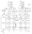
図1を参照すると、一実施形態において、データ記憶装置8は、抵抗性クロスポイントメモリセルアレイ10と、クロスポイントメモリセルアレイ10の行に沿って延在する複数のワード線14と、クロスポイントメモリセルアレイ10の列に沿って延在する複数のビット線16とを含む。メモリセルアレイ10のメモリセル12は、磁気ランダムアクセスメモリ(MRAM)素子、相変化メモリ素子および追記型(たとえば、ヒューズベースまたはアンチヒューズベース)抵抗性メモリ素子を含む多種多様な従来の抵抗性メモリ素子のうちの任意の1つとして実施され得る。
【0016】
また、データ記憶装置8は、複数の読出し回路20も含み、それらの各々は、それぞれのビット線16によりメモリセル12の1つまたは複数の関連するセットに結合される。各読出し回路20は、メモリセル12の関連するグループ(単数または複数)のメモリセルを流れる電流をセンシングするように動作可能である。ステアリング回路22は、受取ったビット線アドレス(AY)に基づいて、関連する読出し回路20を選択されたビット線16に選択的に結合する。各ステアリング回路22は、各ビット線16を定電圧(VA)の電圧源か、または関連する読出し回路20に接続する1組のスイッチを含む。ワード線デコード回路18は、受取ったワード線アドレス(AX)に基づいて特定のワード線14を選択的に活性化する。読出し動作中、ワード線デコード回路18は、選択されたワード線14をアースに接続して他の選択されていないワード線に定電圧(VA)を印加することにより、選択されたワード線14を活性化することができる。各読出し回路20の出力は、データ記憶装置8のそれぞれの入出力(I/O)パッドの入力に結合される。
【0017】
例示の実施形態では、抵抗性クロスポイントメモリセルアレイは、比較的わずかな数のメモリセル12を有するように示される。しかしながら、他の実施形態は、多数のメモリセルを含むことができる。たとえば、一実施形態では、抵抗性クロスポイントメモリセルアレイ10は、メモリセル12の1024×1024のアレイと、各々が4つのビット線16のピッチに適合する256個の読出し回路20とを含む。この実施形態では、合計4つのビット線16を各読出し回路20に多重化することができる。幾つかの実施形態は、多段のメモリセルアレイ12を含むことができる。これらの実施形態では、異なる段からのビット線16を読出し回路20に多重化することができる。
【0018】
幾つかの実施形態において、データ記憶装置8は、抵抗性クロスポイントメモリアレイ10のメモリセル12に情報を書込むための書込み回路(図示せず)も含むことができる。
【0019】
以下に詳述するように、抵抗性クロスポイントメモリセルアレイ10のアーキテクチャは、実用的な寸法と電流密度特性とを有する分離ダイオードにより高密度の製作および高速動作を可能にする。さらに、データ記憶装置8は、メモリセル12の抵抗状態のセンシングに干渉する可能性のある寄生電流を実質的に回避する、新規な等電位分離回路を含む。
【0020】
ここで、図面に示される例示的な実施形態を参照し、本明細書ではそれを説明するために特定の言語を使用する。しかしながら、それにより本発明の範囲の限定も意図されないことが理解されよう。関連する技術分野における当業者およびこの開示を所有する者には思いつくと考えられる、本明細書で例示される本発明の特徴の代替案およびさらなる修正案と、本明細書で例示されるような発明の原理のさらなる応用とは、本発明の範囲内にあるとみなされるできである。
【0021】
例示の目的のために図面に示すように、本発明は、磁気ランダムアクセスメモリデバイスにおいて具現化される。MRAMデバイスは、メモリセルのアレイと、メモリセルからデータを読出すための読出し回路とを含む。読出し回路は、等電位印加装置と差動センス増幅器とを含み、アレイ内の選択されたメモリセルの異なる抵抗状態を確実にセンシングすることができる。
【0022】
ここで図1を参照すると、図1は、メモリセル素子12aおよび12bの抵抗性クロスポイントアレイ10を含む情報記憶装置8を示す。メモリセル素子12aおよび12bは、行および列に配置されており、行はx方向に沿って延在し、列はy方向に沿って延在する。情報記憶装置8の例示を簡略化するために、比較的わずかな数のメモリセル素子12aおよび12bのみを示す。実際には、任意のサイズのアレイを使用できる。
【0023】
ワード線14として機能しているトレースは、メモリセルアレイ10の一方の側の平面においてx方向に沿って延在する。ビット線16aおよび16bとして機能しているトレースは、メモリセルアレイ10の隣接する側の平面においてy方向に沿って延在する。アレイ10の各行に1つのワード線14とアレイ10の各列に1つのビット線16aまたは16bとが存在できる。各メモリセル素子12a、12bは、ワード線14とビット線16aまたは16bとのクロスポイント(交点)に配置される。
【0024】
メモリセル素子12aおよび12bは、磁気トンネル接合(SDT接合は一種の磁気トンネル接合である)か、または相変化デバイス等の薄膜メモリ素子を含むことができる。概して、メモリセル12aおよび12bは、素子の公称抵抗の大きさに影響を与えることにより情報を格納または生成する任意の素子を含むことができる。かかる他のタイプの素子には、リードオンリメモリの一部としてのポリシリコン抵抗と、材料の状態を結晶からアモルファスにおよびその逆に変化させることにより抵抗状態を変化させるようにプログラムすることができる相変化デバイスとが含まれる。
【0025】
SDT接合の抵抗は、たとえば、その磁化の向きが平行である場合には第1の値(R)であり、磁化の向きが平行から反平行に変化した場合には第2の値(R+△R)に増大する。一般的な第1の抵抗値(R)は、約10kΩ〜1MΩとすることができ、抵抗(△R)の一般的な変化は、第1の抵抗値(R)の約30%とすることができる。
【0026】
各メモリセル素子12aおよび12bは、外部電源がない場合であってもその磁化の向きを保持する。したがって、メモリセル素子12aおよび12bは不揮発性である。
【0027】
データは、メモリセル素子12aおよび12bにビット・ビットバー方式で格納される。2つのメモリセル素子12aおよび12bがデータの各ビットに割当てられ、一方のメモリセル素子(「データ」素子)12aがビットの値を格納し、他方のメモリセル素子(「基準」素子)12bが値の補数を格納する。このため、データ素子12aが論理「1」を格納する場合、その対応する基準素子12bは論理「0」を格納する。データ素子12aの各列は、ビット線16aに接続され、基準素子12bの各列は、ビット線16bに接続される。
【0028】
メモリセル12は、いかなる特定のタイプのデバイスに限定されない。MRAM等のスピン依存トンネル効果(SDT)デバイスは、クロスポイントメモリによく適している。通常のSDTデバイスは、「ピン留め(pinned)」層と「フリー」層とを含む。ピン留め層は、平面内で配向されているが、対象となる範囲内に印可された磁界が存在する場合に固定されたままである磁化を有する。フリー層は、印加磁界によって回転させることができる磁化を有し、その向きは「磁化容易軸」に沿っており、ピン留め層の磁化と平行である。フリー層の磁化の向きは、それぞれ低抵抗状態と高抵抗状態とに対応するピン留め層の磁化に対して、図2aに示すように平行であるか、または図2bに示すように反平行である。
【0029】
図1に戻ると、情報記憶装置8は、読出しおよび書込み動作中にワード線14を選択するための行デコーダ18を含む。読出し動作中、選択されたワード線14は接地に接続され得る。書込み動作中、選択されたワード線14に対して書込み電流を印加することができる。
【0030】
情報記憶装置8は、読出し動作中に選択されたメモリセル素子12aおよび12bの抵抗状態をセンシングするための読出し回路と、書込み動作中に選択されたワード線14およびビット線16aおよび16bに電流を供給するための書込み回路とを含む。読出し回路を、概して20で示す。情報記憶装置8の例示を簡略化するために、書込み回路は示していない。
【0031】
読出し回路20は、複数のステアリング回路22とセンス増幅器24とを含む。複数のビット線16が各ステアリング回路22に接続される。各ステアリング回路22は、ビット線を選択するためのデコーダを含む。選択されたメモリセル素子12は、選択されたワード線14と選択されたビット線16との交差点にある。
【0032】
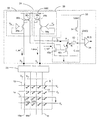
図5のフローチャートにも示す読出し動作中、ブロック504に示すように、選択された素子12aおよび12bは、選択されたワード線14によって接地に接続される。各ステアリング回路22は、データ素子12aの列と交差するビット線16aと、基準素子12bの対応する列と交差するビット線16bとを選択する。データ素子12aの列と交差する選択されたビット線16aは、ブロック502に示すように、それらの対応するセンス増幅器24のセンスノードS0に接続される。ブロック502および504のステップを逆にすることができ、それらの実施の順序は重要ではない。基準素子12bの列と交差する選択されたビット線16bは、それらの対応するセンス増幅器24の基準ノードR0に接続される。各センス増幅器24は、差動前置増幅器と、カレントミラー回路と、電荷注入増幅器と、ビット線16aおよび16b上の信号を比較するための比較器とを含む。比較は、選択されたデータ素子12aの抵抗状態、したがって選択されたデータ素子12aに格納された論理値を示す。センス増幅器24の出力はデータレジスタ26に供給され、データレジスタ26は、情報記憶装置8のI/Oパッド28に結合される。
【0033】
ブロック506に示すように、選択されていないワード線14のすべてが、アレイ電圧(VA)を供給する定電圧源に接続される。外部回路が定電圧源を提供することができる。センス増幅器24は、選択されていないワード線のサブセットに定電圧源が印加するものと同じ電位を、選択されたビット線16に印加する。かかる等電位分離をアレイ10に適用することにより、寄生電流が低減される。
【0034】
読出し回路20は、mビットワードでデータを読出すことができ、それにより、複数(m)のメモリセル素子12aおよび12bの抵抗状態が同時にセンシングされる。それを、ブロック508の電流測定ステップとして示す。m個の連続したセンス増幅器24を同時に動作させることにより、mビットワードを読出すことができる。
【0035】
図3aを参照すると、一実施形態では、抵抗性クロスポイントメモリセルアレイ10のメモリセル12は、2つまたはそれより多いメモリセル12の複数のグループ15に構成される。たとえば、例示の実施形態では、各グループ15は3つのメモリセル12を含む。各グループ15のメモリセル12は、それぞれのビット線16と、ワード線14に結合される共通グループ分離ダイオード13との間に接続される。抵抗性クロスポイントメモリセルアレイ10は、ダイオード分離アーキテクチャに関連する高速動作の利点と、実用的な寸法および電流密度特性を有する分離ダイオードで実施され得るアーキテクチャにおける等電位分離アーキテクチャの高密度の利点とを特徴とする。実施形態によっては、分離ダイオード13を、従来の薄膜ダイオード製作技術を使用してメモリセル12とともに製作することができ、それにより、マルチレベル抵抗性クロスポイントメモリアレイを構成することが可能になる。
【0036】
読出し動作の場合、抵抗性クロスポイントメモリセルアレイ10のターゲットセルにおいて、ターゲットメモリセルに対応するワード線14を選択し、それを接地電位に接続することにより、データがセンシングされる。同時に、ビット線16aおよび16bが、基準/センスのペアで読出し回路20に接続される。アレイ電位(VA)は、電圧源の出力から選択されたグループの選択されていないビット線16に印加される。また、アレイ電位(VA)は、センス増幅器24の入力に印加され、それによって選択されたビット線16aおよび16bに結合電圧(VA’)がもたらされる。結合電圧(VA’)は、実質的にアレイ電圧(VA)に等しい。選択されていないグループのビット線は、フローティングのままである。アレイの上記バイアス状態下では、選択されたグループ15のビットセルのみが、電位電圧VAおよび基準電流I_refにより順方向バイアスされ、結果として、センス電流I_dataがメモリセル12aおよび12bを流れている。それらが増幅器24によってセンシングされることにより、ビットセルの状態が判定される。また、電流は、選択されたグループのビットセルにも流れているが、基準電流およびセンス電流に干渉しない。
【0037】
図3bは、図示するように各メモリセル12が単一の分離ダイオード13に直接的に結合される代替の実施形態を示す。増幅器24を介したアレイ10の動作は、図3aにおいて例示したものと同様であり、以下に説明する。
【0038】
メモリアレイ10において、選択されたワード線14を接地電位に接続し、センス電流および基準電流に対する漏れ電流の影響を最小化するために、選択されていないワード線のすべてを電位(VA)に接続することにより、読出し動作が実行される。選択されたビット線16aおよび16bは、マルチプレクサ22およびノードR0およびS0を介してセンス増幅器24の入力に接続される。センス増幅器の他の入力は、選択されていないワード線と同じ電位(VA)に接続される。このため、選択されたビット線16aおよび16bは、他の選択されていないビット線がフローティングのままである一方で、実質的に(VA)と等しい電位(VA’)にバイアスされる。アレイに対する上記バイアス状態下では、選択されたメモリ12aおよび12bのみが電位電圧(VA)によって順方向にバイアスされ、その結果、基準電流I_refおよびセンス電流I_dataがメモリセル12aおよび12bを流れて、増幅器24によってセンシングされることにより、ビットセルの状態が判定される。
【0039】
さらに、図3cは、分離ダイオードがないメモリセル12を示す。増幅器24によるアレイ10の動作は、分離ダイオードとそれが通常回路全体に課す制限とがないことを除き、図3aのものと同じである。アレイ10において、磁気トンネル接合12は、アレイのビットのセンシングに干渉する多くの並列経路を介して結合される。この問題は、特許文献2に開示された「等電位」方法を使用することによって対処することができ、この「等電位」方法は、選択されたビット線16aおよび16bに電位を印加して、同じ電位を選択されていないビット線16と恐らくは選択されていないワード線14のサブセットに供給することを含む。選択されたワード線14は、接地電位に接続される。したがって、選択されたワード線14に接続された接合のみが、両端に電圧(VA)を有しており、このため、電流はこれらの接合を流れているが、互いに干渉しない。基準電流I_refおよびセンス電流I_dataを、センス増幅器によって正確にセンシングすることができ、したがって格納されたデータビットの状態を判定することができる。
【0040】
図3a、図3bおよび図3cに示す3つの場合のすべてに共通するセンス増幅器24を参照する。動作時、基準ビット線において生成される電流とセンスビット線において生成される電流との間の差を検出することにより、データ「1」またはデータ「0」をセンシングすることができる。実施形態によっては、基準ビット線に関連するいくつかのメモリセルが存在できる。他の実施形態では、ビット毎に1つの基準ビットが存在できる。
【0041】
読出し動作の場合、前置増幅器36は、電圧源(VA)に接続する第1の入力と、トランジスタ36aのゲート入力に結合されたその出力とを有する。トランジスタ36aのソース端と前置増幅器36の第2の入力とが、データビットセル12aが配置されている選択されたビット線16aに結合される。同様に、前置増幅器38の第1の入力は電圧源VAに接続され、その出力はトランジスタ38aのゲート入力に接続される。トランジスタ38aのソース端と前置増幅器38の第2の入力とは、基準ビットセル12bが配置されている選択されたビット線16bに結合される。前置増幅器36および38は、ビット線16aおよび16bの電圧を、実質的に電圧(VA)に等しい電位(VA’)に調整する。このため、選択されたメモリ素子12aおよび12bの各々の両端に、電位(VA)がかかる。その結果、電流I_ref=(VA−Vd)/R12aが選択された素子12aを流れ、電流I_data=(VA−Vd)/R12bが選択された素子12bを流れる。ここで、R12aおよびR12bはメモリセル12の抵抗値であり、Vdはダイオード13の順方向ダイオード電圧であり、通常はおよそ0.7Vである。図3cにおける一実施形態では、メモリアレイ10にはダイオードが存在しないため、この場合Vdは0である。
【0042】
また、I_refおよびI_data電流は、トランジスタ36aおよび38aにも流れている。トランジスタ36b、36c、38b、38c、40aおよび40bは、整合されたトランジスタであり、接続されることによりカレントミラーの3つのセットを形成する。第1のセットは、トランジスタ36bおよび36cからなり、I_refに等しいミラー電流I_ref’を生成する。第2のセットは、トランジスタ40aおよび40bからなり、I_refおよびI_ref’に等しいミラー電流IRを生成する。同様に、第3のセットは、トランジスタ38bおよび38cからなり、I_dataに等しい電流ISを生成する。
【0043】
読出し動作中、読出しイネーブルトランジスタ52がオフとなり、トランジスタ54がイネーブルになりコンデンサCを電圧レベルVdd/2までプリチャージする。その後、トランジスタ54がオフとなり、トランジスタ52がオンとなる。この時点で、ノードAにおける電流を合計すると、IS+IC−IR=0またはIC=IR−ISとなる。コンデンサ電圧は、電流ICによって決まる。電流IRが電流ISより小さい場合、それはセンスセルが低抵抗状態を有し基準セルが高抵抗状態を有することを示し、電流ICはノードAから離れコンデンサCに向かって流れ、コンデンサCをICのレートで充電する。電流IRが電流ISより大きい場合、それはセンスセルが高抵抗状態を有し基準セルが低抵抗状態を有することを示し、電流ICはノードAに向かってコンデンサCから離れるように流れ、コンデンサCをICのレートで放電する。基準電流IRとセンス電流ISとがともに等しい場合、それは、基準セルとセンスセルとがともに同じ抵抗値を有することを意味し、このときコンデンサ電流ICは0であり、このためコンデンサ電圧は変化しない。コンデンサ電圧は、比較器34により基準電圧Vdd/2と比較される。比較器34の低レベル出力は、コンデンサCが充電されており、そのためデータビットセル抵抗が基準ビットセル抵抗より小さいことを示す。高レベル出力は、コンデンサが放電されており、そのためデータビットセル抵抗が基準ビットセル抵抗より大きいことを示す。
【0044】
図4は、読出しシーケンス中のコンデンサ電圧を示す。ここでは、コンデンサ電圧の上昇は、ISセンス電流がIR基準電流より大きく、そのためデータビットセルが低抵抗を有しデータビットが1であることを示し、コンデンサ電圧の下降は、センス電流が基準電流より小さく、そのためデータ素子が高抵抗を有しデータビットが0であることを示す。この技術はまた、複数のセンス増幅器が使用される場合(すなわち、複数のビットペアが同時にセンシングされる場合)に良好に動作する。
【0045】
図3a、図3bおよび図3cに示すように、比較器回路34は、センス増幅器出力信号と基準信号Vdd/2とを比較するように実施され得る。この回路は、アナログ差動センス電圧データを確実なフルスイングデジタルデータに変換する。データ記憶装置10の他のコンポーネントと結合されると、比較器/ラッチ回路34は、センシング動作を完了するために信頼性のある効率的な回路となる。
【0046】
差動電荷注入増幅器を使用することにより、従来技術にまさる利点が得られる。1つの利点は、電荷注入増幅での差動センスにより、より優れたコモンモードノイズ除去が提供されることである。この結果、出力信号がより明瞭でより容易に識別可能となる。さらに、電荷注入センス増幅器が、差動電流(IC)信号のみをセンシングし、そのためより正確であり、より広い動作範囲を有することから、より優れた分解能を提供する。さらに、MTJが互いに接近する場合に同じグループ内の基準MTJを使用することにより、非破壊読出しが可能であり、抵抗をより良好に整合させることができる。
【0047】
さらに、本発明による差動センス増幅器は、従来技術と比較して、カレントミラーと電荷注入増幅器とを含む単純な設計を提供する。これにより、製造コストが低下し、一般に従来のシステムに関連する表面積が低減される。
【0048】
上述の実施形態は本発明の代表例であるが、当業者には、本明細書および特許請求の範囲の検討から、または開示した発明の実施形態の実施から、他の実施形態が明らかとなろう。明細書とその中の実施形態とは、単なる例示としてみなされることが意図されており、本発明は、特許請求の範囲とそれらの等価物とによって規定される。
【0049】
以下においては、本発明の種々の構成要件の組み合わせからなる例示的な実施形態を示す。
1.情報記憶装置であって、
抵抗性クロスポイントメモリセルアレイと、
複数のワード線と、
複数のビット線であって、メモリセルのグループが共通のワード線に接続され、前記グループの各メモリセルが単一のビット線に接続される、複数のビット線と、及び
前記メモリセルアレイに結合された差動センス増幅器とからなり、その差動センス増幅器が、
第1および第2の入力ノードであって、その第1の入力ノードが、前記セルアレイ内の基準セルに接続された前記複数のビット線のうちの1つに選択的に結合され、前記第2の入力ノードが、所与のワード線に共通の前記メモリセルのグループ内のセンスセルに選択的に結合される、第1および第2の入力ノードと、
前記第1の入力ノードに結合される第1の前置増幅器と、
前記第2の入力ノードに結合される第2の前置増幅器と、
前記第1の前置増幅器からの出力と前記第2の前置増幅器からの出力とに結合され、読出し動作中に前記基準セルの抵抗状態と比較して前記センスセルの抵抗状態を判定する電荷注入増幅器とからなる、情報記憶装置。
2.情報記憶装置であって、
抵抗性クロスポイントメモリセルアレイと、
複数のワード線と、
複数のビット線であって、前記メモリセルが2つまたはそれより多いメモリセルの複数のグループに構成され、各グループのメモリセルがそれぞれのワード線とビット線に結合された共通分離ダイオードとの間に接続される、複数のビット線と、及び
前記メモリセルアレイに結合される差動センス増幅器とからなり、その差動センス増幅器が、
第1および第2の入力ノードであって、その第1の入力ノードが、前記セルアレイ内の基準セルに接続された前記複数のビット線のうちの1つに選択的に結合され、前記第2の入力ノードが、前記セルアレイ内のセンスセルに選択的に結合される、第1および第2の入力ノードと、
前記第1の入力ノードに結合された第1の前置増幅器と、
前記第2の入力ノードに結合された第2の前置増幅器と、
前記第1の前置増幅器からの出力と前記第2の前置増幅器からの出力とに結合され、読出し動作中に前記基準セルの抵抗状態と比較して前記センスセルの抵抗状態を判定する電荷注入増幅器とからなる、情報記憶装置。
3.基準回路の抵抗状態の比較に基づいて選択された回路の第1または第2の抵抗状態を判定するために、電荷注入を使用する差動増幅器であって、
前記基準回路に結合された第1の前置増幅器と、
前記選択された回路に結合された第2の前置増幅器と、
前記基準回路からの基準電流に基づいて前記基準電流を受入れるための、前記第1の前置増幅器に結合された第1の入力と、前記選択された回路からのセンス電流に基づいて前記センス電流を受入れるための、前記第2の前置増幅器に結合された第2の入力とを有するカレントミラーと、
前記第2の前置増幅器に結合され、読出し動作に先立って、選択された電位に充電されるプリチャージ回路と、
前記プリチャージ回路に結合され、読出し動作中に、かつ前記プリチャージ回路における前記電位によって影響される際に、前記第2の前置増幅器からの前記センス電流が前記第1の前置増幅器からの前記基準電流より大きい場合、前記第1の抵抗状態を表す第1の出力を提供し、あるいは前記基準電流が前記センス電流より大きい場合、前記第2の抵抗状態を表す第2の出力を提供する、比較器増幅器とからなる、差動増幅器。
4.前記電荷注入増幅器が、前記センスセルを流れる電流を1つまたは複数の基準セルを流れる電流と比較することにより、前記センスセルの抵抗状態を判定する、上記1または2記載の情報記憶装置。
5.各々が、それぞれのビット線によりメモリセルの1つまたは複数の関連するグループに結合され、その関連するグループのメモリセルを流れる電流をセンシングするように動作可能である、複数の読出し回路をさらに含む、上記1または2記載の情報記憶装置。
6.各々が、関連する読出し回路に結合され、アナログ差動センス電圧をデジタル出力読出し信号に変換するように動作可能である、複数の比較器回路をさらに含む、上記1または2記載の情報記憶装置。
7.前記ワード線と前記ビット線とに結合され、選択されたワード線とビット線とにおいて前記抵抗性クロスポイントメモリセルアレイにおける電圧レベルを、選択されていないメモリセルに実質的に寄生電流が流れないように設定するよう動作可能である、等電位発生器をさらに含む、上記1または2記載の情報記憶装置。
8.各メモリセルが、磁気ランダムアクセスメモリ素子からなる、上記1または2記載の情報記憶装置。
9.前記等電位発生器が、選択されていないワード線からのフィードバックによりメモリセルの各グループの前記共通分離ダイオードの入力ノードを設定するように動作可能である、上記7記載の情報記憶装置。
10.前記電荷注入増幅器が、
前記第1の前置増幅器に結合され、前記基準セルからの基準電流に基づいてその基準電流を受入れるための第1の入力と、前記第2の前置増幅器に結合され、前記センスセルからのセンス電流に基づいてそのセンス電流を受入れるための第2の入力とを有するカレントミラーと、
前記第2の前置増幅器に結合され、読出し動作に先立って選択された電位に充電されるプリチャージ回路と、
前記プリチャージ回路と基準電圧とに結合され、読出し動作中に、かつ前記プリチャージ回路における前記電位によって変更される際に、前記第2の前置増幅器からの前記センス電流が、前記第1の前置増幅器からの前記基準電流より大きい場合には、第1の出力を供給し、前記基準電流が前記センス電流より大きい場合には、第2の出力を供給する、比較器増幅器とからなる、上記1または2記載の情報記憶装置。
【0050】
【発明の効果】
本発明によれば、差動電荷注入増幅器を使用することにより、従来技術にまさる利点が得られる。1つの利点は、電荷注入増幅での差動センスにより、より優れたコモンモードノイズ除去が提供されることである。この結果、出力信号がより明瞭でより容易に識別可能となる。さらに、電荷注入センス増幅器が、差動電流(IC)信号のみをセンシングし、そのためより正確であり、より広い動作範囲を有することから、より優れた分解能を提供する。さらに、MTJが互いに接近する場合に同じグループ内の基準MTJを使用することにより、非破壊読出しが可能であり、抵抗をより良好に整合させることができる。
【0051】
さらに、本発明による差動センス増幅器は、従来技術と比較して、カレントミラーと電荷注入増幅器とを含む単純な設計を提供する。これにより、製造コストが簡略化され、一般に従来のシステムに関連する表面積が低減される。
【図面の簡単な説明】
【図1】メモリセルの抵抗性クロスポイントアレイと、複数の読出し回路および関連するステアリング回路と、ワード線デコード回路とを含むデータ記憶装置の回路図である。
【図2a】メモリセルの平行磁化の向きを示す図である。
【図2b】メモリセルの反平行磁化の向きを示す図である。
【図3a】本発明による差動センス回路と比較器とを使用する、グループ抵抗性メモリ素子と共通共有ダイオードとから構成されるアレイ内のメモリセルを流れる電流をセンシングするように動作可能な、センス増幅器回路の回路図である。
【図3b】本発明による差動センス回路と比較器とを使用する、抵抗性/ダイオードメモリアレイ内のメモリセルを流れる電流をセンシングするように動作可能な、センス増幅器回路の回路図である。
【図3c】本発明による差動センス回路と比較器とを使用する、抵抗性メモリアレイ内のメモリセルを流れる電流をセンシングするように動作可能なセンス増幅器回路の回路図である。
【図4】図3A、図3Bおよび図3Cの回路に対する読出しサイクルのタイミング図である。
【図5】図1の抵抗性クロスポイントメモリセルアレイのうちのメモリセルを読出す方法のフローチャートである。
【符号の説明】
8 データ記憶装置
10 抵抗性クロスポイントメモリセルアレイ
12a、12b メモリセル素子
14 ワード線
16 ビット線
18 行デコーダ
24 センス増幅器[0001]
BACKGROUND OF THE INVENTION
The present invention relates generally to resistive crosspoint memory cell arrays, and more particularly to a resistive crosspoint memory cell array having a differential sense amplifier that utilizes a charge injection mode.
[0002]
[Prior art]
Many different resistors, including resistive cross-point memory cell arrays having magnetic random access memory (MRAM) elements, phase change memory elements, polysilicon memory elements and write-once (eg, fuse-based or anti-fuse-based) resistive memory elements Cross-point memory cell arrays have been proposed.
[0003]
For example, a typical MRAM storage device includes an array of memory cells. The word lines can extend along the rows of memory cells, and the bit lines can extend along the columns of memory cells. Each memory cell is arranged at a cross point (intersection) between the word line and the bit line. Each MRAM memory cell stores 1-bit information as the magnetization direction. In particular, the magnetization of each memory cell always takes one of two stable orientations. These two stable orientations, parallel and antiparallel, represent logical values of 0 and 1. The direction of magnetization affects the resistance of the memory cell. For example, the resistance of the memory cell can be a first value “R” if the magnetization direction is parallel, and if the magnetization direction changes from parallel to anti-parallel, the second value can be It can be increased to the value R + ΔR.
[0004]
In general, the logic state of a resistive cross point memory cell can be read by sensing the resistance state of the selected memory cell. However, in general, it is difficult to sense the resistance state of a single memory cell in the array because all of the memory cells of a resistive cross-point memory cell array are interconnected by many parallel paths. The resistance seen at one cross-point is equal to the resistance of the memory cell at that cross-point that is parallel to the resistance of the other word line and bit line memory cells.
[0005]
Thus, one obstacle that must be overcome before a high-density and fast-access resistive cross-point memory can be developed is that while the data stored in the selected memory cell is being sensed. To ensure isolation of the selected resistive cross-point memory cells. In general, conventional techniques for isolating such memory cells become one of three memory cell isolation categories: select transistor isolation techniques, diode isolation techniques, and equipotential isolation techniques.
[0006]
Known transistor isolation techniques generally involve inserting a select transistor in series with each resistive crosspoint memory cell. This architecture is generally characterized by fast read access times. Unfortunately, such series transistor architectures are also generally characterized by relatively poor utilization of the silicon area. The reason is that the area under the resistive crosspoint memory cell array is generally reserved for series transistors and is therefore not available for support circuits. Furthermore, this isolation technique also tends to have a relatively insufficient memory cell layout density. The reason is that a region must be assigned to each memory cell with respect to the via connecting the memory cell to the series transistor in the substrate. This isolation technique also generally requires a relatively high write current. The reason is that in order to provide a write circuit in parallel to the read circuit, a separate write conductor must be added to the memory cell, and depending on the position of the write conductor, to generate the desired write field. This is because a high write current results. In general, this approach is limited to a single memory plane. The reason is that the serial transistor must be placed on the substrate and there is no practical way to move the serial transistor from the substrate into the memory cell plane.
[0007]
Diode isolation techniques generally include inserting a diode in series with each resistive crosspoint memory element. This memory cell array architecture can be implemented with thin film diodes that allow a multi-level resistive cross-point memory array to be constructed (see US Pat. This architecture has the potential for high speed operation. Often the problems associated with this architecture include providing a suitable thin film diode with a minimum process feature size consistent with the potential density of the memory cell array. Furthermore, this approach uses one diode per memory element, and with currently practical MRAM functions and parameters, for example, each diode is 5-15 kA / cm. 2 Is required to be conductive. Such high current densities are generally not practical for implementing thin film diodes in high density MRAM arrays.
[0008]
Equipotential isolation techniques generally involve sensing resistive cross-point memory cells without using series diodes or transistors (see US Pat. This approach can be implemented with a cross-point array of memory elements that are relatively simple to fabricate. This cross-point memory cell array architecture typically has a density that is limited only by the minimum functional size of the circuit technology being implemented, and generally requires a relatively low write current. Furthermore, it is relatively easy to achieve very high density memory by extending this approach to a multi-level resistive cross-point memory cell array. However, equipotential separation is often difficult to implement on large arrays. Auto-calibration and triple-sample readout techniques have been used to sense data in large MRAM arrays using equipotential separation techniques, but these sensing processes generally limit the readout sensing time to a few microseconds To do.
[0009]
[Patent Document 1]
US Pat. No. 5,793,697
[Patent Document 2]
US Pat. No. 6,259,644
[0010]
[Problems to be solved by the invention]
It is an object of the present invention to provide a resistive cross point memory array having a charge injection differential sense amplifier.
[0011]
[Means for Solving the Problems]
In one aspect, the invention features a data storage device that includes a resistive crosspoint array of memory cells, a plurality of word lines, a plurality of bit lines, and a sense amplifier that utilizes an injected charge amplifier. Memory cells are organized into groups of one or more memory cells. The injected charge amplifier determines whether the sensed memory cell is in a first resistance state or a second resistance state compared to a reference cell.
[0012]
The injected charge amplifier can further include a comparator circuit coupled to the associated readout circuit. The comparator circuit is preferably operable to convert the analog differential sense current into a digital output read signal.
[0013]
Other features and advantages of the invention will be apparent from the following description, including the drawings and the claims.
[0014]
DETAILED DESCRIPTION OF THE INVENTION
In the following description, the same reference numbers are used to identify similar elements. Furthermore, the drawings are intended to schematically illustrate the main features of the exemplary embodiments. The drawings are not intended to show every feature of the actual embodiment, or the relative dimensions of the elements shown, but are drawn to scale.
[0015]
Referring to FIG. 1, in one embodiment, a
[0016]
[0017]
In the illustrated embodiment, the resistive cross point memory cell array is shown as having a relatively small number of
[0018]
In some embodiments, the
[0019]
As will be described in detail below, the architecture of the resistive cross-point
[0020]
Reference will now be made to the exemplary embodiment illustrated in the drawings, and specific language will be used herein to describe it. It will be understood, however, that no limitation of the scope of the invention is thereby intended. Alternatives and further modifications of the features of the invention illustrated herein, as would be thought of to those skilled in the relevant arts, and those who own this disclosure, as illustrated herein Further applications of the principles of the invention can be considered to be within the scope of the present invention.
[0021]
As shown in the drawings for purposes of illustration, the present invention is embodied in a magnetic random access memory device. The MRAM device includes an array of memory cells and a read circuit for reading data from the memory cells. The read circuit includes an equipotential application device and a differential sense amplifier, and can reliably sense different resistance states of selected memory cells in the array.
[0022]
Referring now to FIG. 1, FIG. 1 shows an
[0023]
The trace functioning as the
[0024]
[0025]
The resistance of the SDT junction is, for example, a first value (R) when the magnetization direction is parallel, and a second value (R + Δ) when the magnetization direction changes from parallel to antiparallel. R). The general first resistance value (R) can be about 10 kΩ to 1 MΩ, and the general change in resistance (ΔR) is about 30% of the first resistance value (R). Can do.
[0026]
Each
[0027]
Data is stored in the
[0028]
[0029]
Returning to FIG. 1,
[0030]
The
[0031]
The
[0032]
During the read operation also shown in the flowchart of FIG. 5, the selected
[0033]
As shown in
[0034]
The
[0035]
Referring to FIG. 3a, in one embodiment, the
[0036]
In the read operation, data is sensed by selecting the
[0037]
FIG. 3b shows an alternative embodiment in which each
[0038]
In
[0039]
Furthermore, FIG. 3c shows a
[0040]
Reference is made to sense
[0041]
For the read operation, the
[0042]
The I_ref and I_data currents are also flowing through the
[0043]
During the read operation, the read enable
[0044]
FIG. 4 shows the capacitor voltage during the read sequence. Here, the rise in the capacitor voltage is I S Sense current is I R Greater than the reference current, thus indicating that the data bit cell has a low resistance and the data bit is 1, and a drop in the capacitor voltage causes the sense current to be less than the reference current, so the data element has a high resistance and the data bit is Indicates 0. This technique also works well when multiple sense amplifiers are used (ie, when multiple bit pairs are sensed simultaneously).
[0045]
As shown in FIGS. 3a, 3b and 3c, the
[0046]
The use of a differential charge injection amplifier offers advantages over the prior art. One advantage is that differential sensing with charge injection amplification provides better common mode noise rejection. As a result, the output signal is clearer and easier to identify. In addition, a charge injection sense amplifier is provided with differential current (I C ) Sensing only the signal, so it is more accurate and has a wider operating range, thus providing better resolution. Further, by using reference MTJs in the same group when MTJs are close together, non-destructive readout is possible and resistances can be better matched.
[0047]
Furthermore, the differential sense amplifier according to the present invention provides a simple design including a current mirror and a charge injection amplifier compared to the prior art. This reduces manufacturing costs and generally reduces the surface area associated with conventional systems.
[0048]
While the above-described embodiments are representative examples of the present invention, other embodiments will become apparent to those skilled in the art from a review of the specification and claims, or from the practice of the disclosed embodiments. Let's go. It is intended that the specification and embodiments therein be considered as exemplary only, and the present invention be defined by the claims and their equivalents.
[0049]
In the following, exemplary embodiments consisting of combinations of various components of the present invention are shown.
1. An information storage device,
A resistive cross-point memory cell array;
Multiple word lines,
A plurality of bit lines, wherein a group of memory cells are connected to a common word line, and each memory cell of the group is connected to a single bit line; and
A differential sense amplifier coupled to the memory cell array, the differential sense amplifier comprising:
First and second input nodes, wherein the first input node is selectively coupled to one of the plurality of bit lines connected to a reference cell in the cell array; First and second input nodes that are selectively coupled to sense cells in the group of memory cells common to a given word line;
A first preamplifier coupled to the first input node;
A second preamplifier coupled to the second input node;
Charge injection coupled to the output from the first preamplifier and the output from the second preamplifier to determine the resistance state of the sense cell relative to the resistance state of the reference cell during a read operation An information storage device comprising an amplifier.
2. An information storage device,
A resistive cross-point memory cell array;
Multiple word lines,
A plurality of bit lines, wherein the memory cells are configured into a plurality of groups of two or more memory cells, each group of memory cells being connected to a respective word line and a common isolation diode coupled to the bit line; A plurality of bit lines connected between, and
A differential sense amplifier coupled to the memory cell array, the differential sense amplifier comprising:
First and second input nodes, wherein the first input node is selectively coupled to one of the plurality of bit lines connected to a reference cell in the cell array; First and second input nodes that are selectively coupled to sense cells in the cell array;
A first preamplifier coupled to the first input node;
A second preamplifier coupled to the second input node;
Charge injection coupled to the output from the first preamplifier and the output from the second preamplifier to determine the resistance state of the sense cell relative to the resistance state of the reference cell during a read operation An information storage device comprising an amplifier.
3. A differential amplifier that uses charge injection to determine a first or second resistance state of a selected circuit based on a comparison of resistance states of a reference circuit;
A first preamplifier coupled to the reference circuit;
A second preamplifier coupled to the selected circuit;
A first input coupled to the first preamplifier for receiving the reference current based on a reference current from the reference circuit; and the sense current based on a sense current from the selected circuit. A current mirror having a second input coupled to the second preamplifier for receiving
A precharge circuit coupled to the second preamplifier and charged to a selected potential prior to a read operation;
The sense current from the second preamplifier is coupled from the first preamplifier when coupled to the precharge circuit and during a read operation and when affected by the potential in the precharge circuit. If greater than the reference current, provide a first output representative of the first resistance state, or provide a second output representative of the second resistance state if the reference current is greater than the sense current. A differential amplifier comprising a comparator amplifier.
4). 3. The information storage device according to
5. A plurality of read circuits each coupled to one or more associated groups of memory cells by respective bit lines and operable to sense current flowing through the associated group of memory cells; The information storage device according to 1 or 2 above.
6). 3. The information storage device of
7). The voltage level in the resistive cross-point memory cell array is coupled to the word line and the bit line so that substantially no parasitic current flows in the unselected memory cells. 3. The information storage device according to
8). 3. The information storage device according to 1 or 2 above, wherein each memory cell comprises a magnetic random access memory element.
9. 8. The information storage device according to claim 7, wherein the equipotential generator is operable to set an input node of the common isolation diode in each group of memory cells by feedback from an unselected word line.
10. The charge injection amplifier comprises:
A first input coupled to the first preamplifier and adapted to accept the reference current based on a reference current from the reference cell; and coupled to the second preamplifier and sensed from the sense cell. A current mirror having a second input for receiving the sense current based on the current;
A precharge circuit coupled to the second preamplifier and charged to a selected potential prior to a read operation;
The sense current from the second preamplifier is coupled to the precharge circuit and a reference voltage, and during the read operation and when changed by the potential in the precharge circuit, A comparator amplifier that provides a first output if greater than the reference current from a preamplifier, and a second output if the reference current is greater than the sense current; 3. The information storage device according to 1 or 2 above.
[0050]
【The invention's effect】
In accordance with the present invention, the use of a differential charge injection amplifier provides advantages over the prior art. One advantage is that differential sensing with charge injection amplification provides better common mode noise rejection. As a result, the output signal is clearer and easier to identify. In addition, a charge injection sense amplifier is provided with differential current (I C ) Sensing only the signal, so it is more accurate and has a wider operating range, thus providing better resolution. Further, by using reference MTJs in the same group when MTJs are close together, non-destructive readout is possible and resistances can be better matched.
[0051]
Furthermore, the differential sense amplifier according to the present invention provides a simple design including a current mirror and a charge injection amplifier compared to the prior art. This simplifies manufacturing costs and generally reduces the surface area associated with conventional systems.
[Brief description of the drawings]
FIG. 1 is a circuit diagram of a data storage device including a resistive crosspoint array of memory cells, a plurality of read circuits and associated steering circuits, and a word line decode circuit.
FIG. 2a is a diagram showing the direction of parallel magnetization of a memory cell.
FIG. 2b is a diagram showing the direction of antiparallel magnetization of a memory cell.
FIG. 3a is operable to sense current flowing through a memory cell in an array composed of a group resistive memory element and a common shared diode using a differential sense circuit and a comparator according to the present invention; It is a circuit diagram of a sense amplifier circuit.
FIG. 3b is a circuit diagram of a sense amplifier circuit operable to sense current flowing through a memory cell in a resistive / diode memory array using a differential sense circuit and a comparator according to the present invention.
FIG. 3c is a circuit diagram of a sense amplifier circuit operable to sense current flowing through memory cells in a resistive memory array using a differential sense circuit and a comparator according to the present invention.
FIG. 4 is a timing diagram of a read cycle for the circuits of FIGS. 3A, 3B and 3C.
FIG. 5 is a flowchart of a method for reading a memory cell of the resistive cross point memory cell array of FIG. 1;
[Explanation of symbols]
8 Data storage
10 Resistive cross-point memory cell array
12a, 12b Memory cell element
14 word lines
16 bit line
18-line decoder
24 sense amplifiers
Claims (19)
抵抗性クロスポイントメモリセルアレイと、
複数のワード線と、
複数のビット線であって、メモリセルのグループが共通のワード線に接続され、前記グループの各メモリセルが単一のビット線に接続される、複数のビット線と、及び
前記メモリセルアレイに結合された差動センス増幅器とからなり、その差動センス増幅器が、
第1および第2の入力ノードであって、その第1の入力ノードが、前記セルアレイ内の基準セルに接続された前記複数のビット線のうちの1つに選択的に結合され、前記第2の入力ノードが、所与のワード線に共通の前記メモリセルのグループ内のセンスセルに選択的に結合される、第1および第2の入力ノードと、
前記第1の入力ノードに結合される第1の前置増幅器と、
前記第2の入力ノードに結合される第2の前置増幅器と、
前記第1の前置増幅器からの出力と前記第2の前置増幅器からの出力とに結合され、読出し動作中に前記基準セルの抵抗状態と比較して前記センスセルの抵抗状態を判定する電荷注入増幅器とからなり、
前記電荷注入増幅器が、
前記第1の前置増幅器に結合され、前記基準セルからの基準電流に基づいた基準電流を受入れるための第1の入力と、前記第2の前置増幅器に結合され、前記センスセルからのセンス電流に基づいたセンス電流を受入れるための第2の入力とを有し、前記基準電流と前記センス電流の差に相当する出力電流を出力するカレントミラーと、
前記カレントミラーの第2の入力に結合され、読出し動作に先立って基準電圧に充電されるプリチャージ回路と、
前記プリチャージ回路と前記基準電圧とに結合され、読出し動作中に、前記第2の前置増幅器からの前記センス電流が、前記第1の前置増幅器からの前記基準電流より大きい場合に、前記出力電流により前記プリチャージ回路の電位が変更されたところに従い第1の出力を供給し、あるいは前記基準電流が前記センス電流より大きい場合に、前記出力電流により前記プリチャージ回路の電位が変更されたところに従い第2の出力を供給する、比較器とからなる、情報記憶装置。An information storage device,
A resistive cross-point memory cell array;
Multiple word lines,
A plurality of bit lines, wherein a group of memory cells are connected to a common word line, each memory cell of the group is connected to a single bit line, and coupled to the memory cell array Differential sense amplifier, and the differential sense amplifier is
First and second input nodes, wherein the first input node is selectively coupled to one of the plurality of bit lines connected to a reference cell in the cell array; First and second input nodes that are selectively coupled to sense cells in the group of memory cells common to a given word line;
A first preamplifier coupled to the first input node;
A second preamplifier coupled to the second input node;
Charge injection coupled to the output from the first preamplifier and the output from the second preamplifier to determine the resistance state of the sense cell relative to the resistance state of the reference cell during a read operation An amplifier,
The charge injection amplifier comprises:
A first input coupled to the first preamplifier and adapted to receive a reference current based on a reference current from the reference cell; and a sense current from the sense cell coupled to the second preamplifier. a current mirror have a second input for receiving a sense current, and outputs an output current corresponding to the difference between the reference current and the sense current based on,
A precharge circuit coupled to a second input of the current mirror and charged to a reference voltage prior to a read operation;
Coupled to said a precharge circuit and the reference voltage, during the read operation, the sense current from the second preamplifier, if the reference current is greater than from the first preamplifier, the potential of the precharge circuit supplies a first output in accordance with what has changed from the output current, or if the reference current is greater than the sense current, the potential of the precharge circuit is changed by the output current where accordance second supplying output, and a comparator, the information storage device.
前記電荷注入増幅器のカレントミラーが、前記ミラー基準電流を受入れるために前記第1のカレントミラーに結合された前記第1の入力と、前記ミラーセンス電流を受入れるために前記第2のカレントミラーに結合された前記第2の入力とを有し、
前記プリチャージ回路が、第1のゲートを介して前記第2の入力に結合され、かつ第2のゲートを介して前記基準電圧に結合されたコンデンサを含み、
前記比較器が、前記コンデンサに結合された第1の比較入力と、前記基準電圧を受入れるための第2の比較入力と、出力とを含み、
読出し動作中に、前記ミラー基準電流と前記ミラーセンス電流との電流差に応じて、前記コンデンサが充電または放電され、前記比較器が、前記充電または放電された後のコンデンサ電圧を前記基準電圧と比較して、前記センスセルの抵抗状態の結果を出力する、請求項1に記載の情報記憶装置。A first current mirror coupled to the first preamplifier for outputting a mirror reference current of a reference current flowing through the reference cell; and a sense coupled to the second preamplifier for flowing through the sense cell. A second current mirror that outputs a mirror sense current of the current;
A current mirror of the charge injection amplifier is coupled to the first input coupled to the first current mirror for receiving the mirror reference current and to the second current mirror for receiving the mirror sense current. Said second input, and
The precharge circuit includes a capacitor coupled to the second input via a first gate and to the reference voltage via a second gate;
The comparator comprises first comparison input coupled to the capacitor, a second comparator input for receiving said reference voltage, and an output,
During the read operation, the capacitor is charged or discharged according to a current difference between the mirror reference current and the mirror sense current, and the comparator uses the capacitor voltage after the charge or discharge as the reference voltage. The information storage device according to claim 1, wherein the result of the resistance state of the sense cell is output in comparison.
抵抗性クロスポイントメモリセルアレイと、
複数のワード線と、
複数のビット線であって、前記メモリセルが2つまたはそれより多いメモリセルの複数のグループに構成され、各グループの各メモリセルがそれぞれのビット線と共通のワード線に結合された共通分離ダイオードとの間に接続される、複数のビット線と、及び
前記メモリセルアレイに結合される差動センス増幅器とからなり、その差動センス増幅器が、
第1および第2の入力ノードであって、その第1の入力ノードが、前記メモリセルアレイ内の基準セルに接続された前記複数のビット線のうちの1つに選択的に結合され、前記第2の入力ノードが、前記メモリセルアレイ内のセンスセルに選択的に結合される、第1および第2の入力ノードと、
前記第1の入力ノードに結合された第1の前置増幅器と、
前記第2の入力ノードに結合された第2の前置増幅器と、
前記第1の前置増幅器からの出力と前記第2の前置増幅器からの出力とに結合され、読出し動作中に前記基準セルの抵抗状態と比較して前記センスセルの抵抗状態を判定する電荷注入増幅器とからなり、
前記電荷注入増幅器が、
前記第1の前置増幅器に結合され、前記基準セルからの基準電流に基づいた基準電流を受入れるための第1の入力と、前記第2の前置増幅器に結合され、前記センスセルからのセンス電流に基づいたセンス電流を受入れるための第2の入力とを有し、前記基準電流と前記センス電流の差に相当する出力電流を出力するカレントミラーと、
前記カレントミラーの第2の入力に結合され、読出し動作に先立って基準電圧に充電されるプリチャージ回路と、
前記プリチャージ回路と前記基準電圧とに結合され、読出し動作中に、前記第2の前置増幅器からの前記センス電流が、前記第1の前置増幅器からの前記基準電流より大きい場合に、前記出力電流により前記プリチャージ回路の電位が変更されたところに従い第1の出力を供給し、あるいは前記基準電流が前記センス電流より大きい場合に、前記出力電流により前記プリチャージ回路の電位が変更されたところに従い第2の出力を供給する、比較器とからなる、情報記憶装置。An information storage device,
A resistive cross-point memory cell array;
Multiple word lines,
A plurality of bit lines, wherein the memory cells are organized into groups of two or more memory cells, and each memory cell of each group is coupled to a respective bit line and a common word line A plurality of bit lines connected to the diode, and a differential sense amplifier coupled to the memory cell array, the differential sense amplifier being
First and second input nodes, wherein the first input node is selectively coupled to one of the plurality of bit lines connected to a reference cell in the memory cell array; First and second input nodes, wherein two input nodes are selectively coupled to sense cells in the memory cell array;
A first preamplifier coupled to the first input node;
A second preamplifier coupled to the second input node;
Charge injection coupled to the output from the first preamplifier and the output from the second preamplifier to determine the resistance state of the sense cell relative to the resistance state of the reference cell during a read operation An amplifier,
The charge injection amplifier comprises:
A first input coupled to the first preamplifier and adapted to receive a reference current based on a reference current from the reference cell; and a sense current from the sense cell coupled to the second preamplifier. a current mirror have a second input for receiving a sense current, and outputs an output current corresponding to the difference between the reference current and the sense current based on,
A precharge circuit coupled to a second input of the current mirror and charged to a reference voltage prior to a read operation;
Coupled to said a precharge circuit and the reference voltage, during the read operation, the sense current from the second preamplifier, if the reference current is greater than from the first preamplifier, the potential of the precharge circuit supplies a first output in accordance with what has changed from the output current, or if the reference current is greater than the sense current, the potential of the precharge circuit is changed by the output current where accordance second supplying output, and a comparator, the information storage device.
前記電荷注入増幅器のカレントミラーが、前記ミラー基準電流を受入れるために前記第1のカレントミラーに結合された前記第1の入力と、前記ミラーセンス電流を受入れるために前記第2のカレントミラーに結合された前記第2の入力とを有し、
前記プリチャージ回路が、第1のゲートを介して前記第2の入力に結合され、かつ第2のゲートを介して前記基準電圧に結合されたコンデンサを含み、
前記比較器が、前記コンデンサに結合された第1の比較入力と、前記基準電圧を受入れるための第2の比較入力と、出力とを含み、
読出し動作中に、前記ミラー基準電流と前記ミラーセンス電流との電流差に応じて、前記コンデンサが充電または放電され、前記比較器が、前記充電または放電された後のコンデンサ電圧を前記基準電圧と比較して、前記センスセルの抵抗状態の結果を出力する、請求項9に記載の情報記憶装置。A first current mirror coupled to the first preamplifier for outputting a mirror reference current of a reference current flowing through the reference cell; and a sense coupled to the second preamplifier for flowing through the sense cell. A second current mirror that outputs a mirror sense current of the current;
A current mirror of the charge injection amplifier is coupled to the first input coupled to the first current mirror for receiving the mirror reference current and to the second current mirror for receiving the mirror sense current. Said second input, and
The precharge circuit includes a capacitor coupled to the second input via a first gate and to the reference voltage via a second gate;
The comparator comprises first comparison input coupled to the capacitor, a second comparator input for receiving said reference voltage, and an output,
During the read operation, the capacitor is charged or discharged according to a current difference between the mirror reference current and the mirror sense current, and the comparator uses the capacitor voltage after the charge or discharge as the reference voltage. The information storage device according to claim 9, wherein the information storage device outputs a result of a resistance state of the sense cell in comparison.
前記基準回路に結合された第1の前置増幅器と、
前記選択された回路に結合された第2の前置増幅器と、
前記基準回路からの基準電流に基づいた基準電流を受入れるための、前記第1の前置増幅器に結合された第1の入力と、前記選択された回路からのセンス電流に基づいたセンス電流を受入れるための、前記第2の前置増幅器に結合された第2の入力とを有し、前記基準電流と前記センス電流の差に相当する出力電流を出力するカレントミラーと、
前記カレントミラーの第2の入力に結合され、読出し動作に先立って、基準電圧に充電されるプリチャージ回路と、
前記プリチャージ回路と前記基準電圧とに結合され、読出し動作中に、前記第2の前置増幅器からの前記センス電流が前記第1の前置増幅器からの前記基準電流より大きい場合に、前記出力電流により前記プリチャージ回路の電位が変更されたところに従い、前記第1の抵抗状態を表す第1の出力を提供し、あるいは前記基準電流が前記センス電流より大きい場合に、前記出力電流により前記プリチャージ回路の電位が変更されたところに従い、前記第2の抵抗状態を表す第2の出力を提供する、比較器とからなる、差動増幅器。A differential amplifier that uses charge injection to determine a first or second resistance state of a selected circuit based on a comparison of resistance states of a reference circuit;
A first preamplifier coupled to the reference circuit;
A second preamplifier coupled to the selected circuit;
A first input coupled to the first preamplifier for receiving a reference current based on a reference current from the reference circuit and a sense current based on a sense current from the selected circuit. a current mirror second have a an input coupled to a preamplifier, and outputs an output current corresponding to the difference between the reference current and the sense current of said second end,
A precharge circuit coupled to a second input of the current mirror and charged to a reference voltage prior to a read operation;
Coupled to said a precharge circuit and the reference voltage, during the read operation, if the reference current is greater than from the sense current of the first preamplifier from the second preamplifier, the output according when the potential of the precharge circuit is changed by the current, to provide a first output indicative of the first resistance state, or when the reference current is greater than the sense current, the pre-by the output current according when the potential of the charge circuit is changed, providing a second output representative of said second resistance state, and a comparator, a differential amplifier.
前記電荷注入増幅器のカレントミラーが、前記ミラー基準電流を受入れるために前記第1のカレントミラーに結合された前記第1の入力と、前記ミラーセンス電流を受入れるために前記第2のカレントミラーに結合された前記第2の入力とを有し、
前記プリチャージ回路が、第1のゲートを介して前記第2の入力に結合され、かつ第2のゲートを介して前記基準電圧に結合されてコンデンサを含み、
前記比較器が、前記コンデンサに結合された第1の比較入力と、前記基準電圧を受入れるための第2の比較入力と、出力とを含み、
読出し動作中に、前記ミラー基準電流と前記ミラーセンス電流との電流差に応じて、前記コンデンサが充電または放電され、前記比較器が、前記充電または放電された後のコンデンサ電圧を前記基準電圧と比較して、前記センスセルの抵抗状態の結果を出力する、請求項17に記載の情報記憶装置。A first current mirror coupled to the first preamplifier for outputting a mirror reference current of a reference current flowing through the reference cell; and a sense coupled to the second preamplifier for flowing through the sense cell. A second current mirror that outputs a mirror sense current of the current;
A current mirror of the charge injection amplifier is coupled to the first input coupled to the first current mirror for receiving the mirror reference current and to the second current mirror for receiving the mirror sense current. Said second input, and
The precharge circuit includes a capacitor coupled to the second input via a first gate and to the reference voltage via a second gate;
The comparator comprises first comparison input coupled to the capacitor, a second comparator input for receiving said reference voltage, and an output,
During the read operation, the capacitor is charged or discharged according to a current difference between the mirror reference current and the mirror sense current, and the comparator uses the capacitor voltage after the charge or discharge as the reference voltage. The information storage device according to claim 17, wherein the information storage device outputs a result of a resistance state of the sense cell in comparison.
Applications Claiming Priority (2)
| Application Number | Priority Date | Filing Date | Title |
|---|---|---|---|
| US10/136782 | 2002-04-30 | ||
| US10/136,782 US6597598B1 (en) | 2002-04-30 | 2002-04-30 | Resistive cross point memory arrays having a charge injection differential sense amplifier |
Publications (3)
| Publication Number | Publication Date |
|---|---|
| JP2003323791A JP2003323791A (en) | 2003-11-14 |
| JP2003323791A5 JP2003323791A5 (en) | 2005-05-12 |
| JP4113033B2 true JP4113033B2 (en) | 2008-07-02 |
Family
ID=22474333
Family Applications (1)
| Application Number | Title | Priority Date | Filing Date |
|---|---|---|---|
| JP2003119280A Expired - Fee Related JP4113033B2 (en) | 2002-04-30 | 2003-04-24 | Resistive crosspoint memory array with charge injection differential sense amplifier |
Country Status (6)
| Country | Link |
|---|---|
| US (1) | US6597598B1 (en) |
| EP (1) | EP1359586A2 (en) |
| JP (1) | JP4113033B2 (en) |
| KR (1) | KR100939068B1 (en) |
| CN (1) | CN100483540C (en) |
| TW (1) | TW200305878A (en) |
Families Citing this family (68)
| Publication number | Priority date | Publication date | Assignee | Title |
|---|---|---|---|---|
| CA2277717C (en) * | 1999-07-12 | 2006-12-05 | Mosaid Technologies Incorporated | Circuit and method for multiple match detection in content addressable memories |
| US6577525B2 (en) * | 2001-08-28 | 2003-06-10 | Micron Technology, Inc. | Sensing method and apparatus for resistance memory device |
| DE60205569T2 (en) * | 2001-12-21 | 2006-05-18 | Kabushiki Kaisha Toshiba | MRAM with stacked memory cells |
| JP2004023062A (en) * | 2002-06-20 | 2004-01-22 | Nec Electronics Corp | Semiconductor device and method for manufacturing the same |
| US7152800B2 (en) * | 2002-08-22 | 2006-12-26 | Texas Instruments Incorporated | Preamplifier system having programmable resistance |
| US6885600B2 (en) * | 2002-09-10 | 2005-04-26 | Silicon Storage Technology, Inc. | Differential sense amplifier for multilevel non-volatile memory |
| US7038960B2 (en) * | 2002-09-10 | 2006-05-02 | Silicon Storage Technology, Inc. | High speed and high precision sensing for digital multilevel non-volatile memory system |
| US6778420B2 (en) * | 2002-09-25 | 2004-08-17 | Ovonyx, Inc. | Method of operating programmable resistant element |
| US6674679B1 (en) * | 2002-10-01 | 2004-01-06 | Hewlett-Packard Development Company, L.P. | Adjustable current mode differential amplifier for multiple bias point sensing of MRAM having equi-potential isolation |
| ITMI20030075A1 (en) * | 2003-01-20 | 2004-07-21 | Simicroelectronics S R L | PARALLEL DETECTION AMPLIFIER WITH CURRENT MIRROR TO BE MEASURED ON EACH REFERENCE BRANCH. |
| US6795359B1 (en) * | 2003-06-10 | 2004-09-21 | Micron Technology, Inc. | Methods and apparatus for measuring current as in sensing a memory cell |
| FR2871279A1 (en) * | 2004-06-03 | 2005-12-09 | Spintron Sa | MAGNETIC MEMORY HAVING MULTIPLE MAGNET MODULES |
| FR2871280A1 (en) * | 2004-06-03 | 2005-12-09 | Spintron Sa | MAGNETIC MEMORY WITH CONFINEMENT CHANNEL |
| JP4118845B2 (en) | 2004-07-30 | 2008-07-16 | 株式会社東芝 | Semiconductor memory device |
| US7224598B2 (en) * | 2004-09-02 | 2007-05-29 | Hewlett-Packard Development Company, L.P. | Programming of programmable resistive memory devices |
| US7130235B2 (en) * | 2004-09-03 | 2006-10-31 | Hewlett-Packard Development Company, L.P. | Method and apparatus for a sense amplifier |
| US7212432B2 (en) * | 2004-09-30 | 2007-05-01 | Infineon Technologies Ag | Resistive memory cell random access memory device and method of fabrication |
| JP2006127583A (en) * | 2004-10-26 | 2006-05-18 | Elpida Memory Inc | Nonvolatile semiconductor memory device and phase changing memory |
| JP4783002B2 (en) | 2004-11-10 | 2011-09-28 | 株式会社東芝 | Semiconductor memory device |
| US7158431B2 (en) | 2005-03-28 | 2007-01-02 | Silicon Storage Technology, Inc. | Single transistor sensing and double transistor sensing for flash memory |
| US7453715B2 (en) * | 2005-03-30 | 2008-11-18 | Ovonyx, Inc. | Reading a phase change memory |
| US7447055B2 (en) * | 2005-04-22 | 2008-11-04 | Hewlett-Packard Development Company, L.P. | Multiplexer interface to a nanoscale-crossbar |
| US7426131B2 (en) * | 2005-11-01 | 2008-09-16 | Adesto Technologies | Programmable memory device circuit |
| US7495971B2 (en) * | 2006-04-19 | 2009-02-24 | Infineon Technologies Ag | Circuit and a method of determining the resistive state of a resistive memory cell |
| WO2008056294A1 (en) * | 2006-11-08 | 2008-05-15 | Nxp B.V. | Read enhancement for memory |
| US7567462B2 (en) * | 2006-11-16 | 2009-07-28 | Micron Technology, Inc. | Method and system for selectively limiting peak power consumption during programming or erase of non-volatile memory devices |
| US7400521B1 (en) | 2007-01-12 | 2008-07-15 | Qimoda Ag | Integrated circuit, memory chip and method of evaluating a memory state of a resistive memory cell |
| DE102007001859B3 (en) * | 2007-01-12 | 2008-04-24 | Qimonda Ag | Integrated circuit e.g. dynamic RAM, for use in electronic device, has resistive memory cell, and p-channel transistor that produces predetermined reading voltage for smaller resistance range which has reference conditions of reference cell |
| US9135962B2 (en) * | 2007-06-15 | 2015-09-15 | Micron Technology, Inc. | Comparators for delta-sigma modulators |
| TWI402847B (en) | 2007-06-25 | 2013-07-21 | Higgs Opl Capital Llc | Sensing circuits of phase change memory |
| KR100919565B1 (en) * | 2007-07-24 | 2009-10-01 | 주식회사 하이닉스반도체 | Phase change memory device |
| US7564707B2 (en) * | 2007-08-22 | 2009-07-21 | Zerog Wireless, Inc. | One-time programmable non-volatile memory |
| CN101802921B (en) * | 2007-09-10 | 2013-08-28 | 松下电器产业株式会社 | Nonvolatile storage apparatus and method for writing data into nonvolatile storage apparatus |
| KR100895387B1 (en) * | 2007-10-16 | 2009-04-30 | 주식회사 하이닉스반도체 | Phase change memory device |
| TWI347607B (en) | 2007-11-08 | 2011-08-21 | Ind Tech Res Inst | Writing system and method for a phase change memory |
| US20110226148A1 (en) * | 2008-05-16 | 2011-09-22 | Sawka Wayne N | Physical destruction of electrical device and methods for triggering same |
| TWI402845B (en) | 2008-12-30 | 2013-07-21 | Higgs Opl Capital Llc | Verification circuits and methods for phase change memory |
| TWI412124B (en) | 2008-12-31 | 2013-10-11 | Higgs Opl Capital Llc | Phase change memory |
| US8514637B2 (en) * | 2009-07-13 | 2013-08-20 | Seagate Technology Llc | Systems and methods of cell selection in three-dimensional cross-point array memory devices |
| US8363450B2 (en) * | 2009-07-13 | 2013-01-29 | Seagate Technology Llc | Hierarchical cross-point array of non-volatile memory |
| JP5284225B2 (en) * | 2009-09-01 | 2013-09-11 | 株式会社東芝 | Nonvolatile semiconductor memory device and reading method thereof |
| US8570785B2 (en) * | 2010-05-26 | 2013-10-29 | Hewlett-Packard Development Company | Reading a memory element within a crossbar array |
| US20140153318A1 (en) * | 2011-07-22 | 2014-06-05 | Frederick Perner | Circuit and method for reading a resistive switching device in an array |
| US8687398B2 (en) | 2012-02-29 | 2014-04-01 | International Business Machines Corporation | Sense scheme for phase change material content addressable memory |
| CN103366804B (en) * | 2012-03-30 | 2017-10-13 | 硅存储技术公司 | The Nonvolatile memory devices of sense amplifier are injected with electric current |
| US9070424B2 (en) * | 2012-06-29 | 2015-06-30 | Samsung Electronics Co., Ltd. | Sense amplifier circuitry for resistive type memory |
| CN104395963A (en) * | 2012-07-27 | 2015-03-04 | 惠普发展公司,有限责任合伙企业 | Dynamic sense circuitry |
| JP5839201B2 (en) | 2013-03-06 | 2016-01-06 | ソニー株式会社 | Semiconductor device and information reading method |
| US10049733B2 (en) * | 2014-10-31 | 2018-08-14 | Hewlett Packard Enterprise Development Lp | Reusing sneak current in accessing memory cells |
| US9489999B2 (en) | 2014-11-26 | 2016-11-08 | Qualcomm Incorporated | Magnetic tunnel junction resistance comparison based physical unclonable function |
| US9478308B1 (en) * | 2015-05-26 | 2016-10-25 | Intel IP Corporation | Programmable memory device sense amplifier |
| EP3341940A1 (en) * | 2015-08-27 | 2018-07-04 | King Abdullah University Of Science And Technology | Read method compensating parasitic sneak currents in a crossbar memristive memory |
| US9852790B1 (en) | 2016-10-26 | 2017-12-26 | International Business Machines Corporation | Circuit methodology for highly linear and symmetric resistive processing unit |
| CN108154227B (en) * | 2016-12-06 | 2020-06-23 | 上海磁宇信息科技有限公司 | Neural network chip using analog computation |
| US10680105B2 (en) | 2017-03-21 | 2020-06-09 | International Business Machines Corporation | Mobile ferroelectric single domain wall implementation of a symmetric resistive processing unit |
| US10261977B2 (en) * | 2017-05-04 | 2019-04-16 | University Of Rochester | Resistive memory accelerator |
| CN110169204B (en) | 2017-05-27 | 2021-04-20 | 李玉麟 | Drive system |
| US10290327B2 (en) | 2017-10-13 | 2019-05-14 | Nantero, Inc. | Devices and methods for accessing resistive change elements in resistive change element arrays |
| US10403336B2 (en) | 2017-12-28 | 2019-09-03 | Micron Technology, Inc. | Techniques for precharging a memory cell |
| TWI687132B (en) * | 2018-05-03 | 2020-03-01 | 李玉麟 | Driver device |
| US11309005B2 (en) * | 2018-10-31 | 2022-04-19 | Taiwan Semiconductor Manufacturing Co., Ltd. | Current steering in reading magnetic tunnel junction |
| US11416416B2 (en) * | 2019-01-13 | 2022-08-16 | Ememory Technology Inc. | Random code generator with non-volatile memory |
| KR20200141887A (en) | 2019-06-11 | 2020-12-21 | 에스케이하이닉스 주식회사 | Semiconductor memory device including a control circuit for controlling a read operation |
| US11217281B2 (en) * | 2020-03-12 | 2022-01-04 | Ememory Technology Inc. | Differential sensing device with wide sensing margin |
| US11817163B2 (en) | 2020-07-16 | 2023-11-14 | Changxin Memory Technologies, Inc. | Circuit for detecting state of anti-fuse storage unit and memory device thereof |
| US11817159B2 (en) | 2020-07-16 | 2023-11-14 | Changxin Memory Technologies, Inc. | Circuit for detecting anti-fuse memory cell state and memory |
| CN113948142B (en) | 2020-07-16 | 2023-09-12 | 长鑫存储技术有限公司 | Antifuse memory cell state detection circuit and memory |
| US11854633B2 (en) | 2020-07-16 | 2023-12-26 | Changxin Memory Technologies, Inc. | Anti-fuse memory cell state detection circuit and memory |
Family Cites Families (8)
| Publication number | Priority date | Publication date | Assignee | Title |
|---|---|---|---|---|
| US5640343A (en) | 1996-03-18 | 1997-06-17 | International Business Machines Corporation | Magnetic memory array using magnetic tunnel junction devices in the memory cells |
| US6169686B1 (en) | 1997-11-20 | 2001-01-02 | Hewlett-Packard Company | Solid-state memory with magnetic storage cells |
| US6259644B1 (en) * | 1997-11-20 | 2001-07-10 | Hewlett-Packard Co | Equipotential sense methods for resistive cross point memory cell arrays |
| US6292389B1 (en) | 1999-07-19 | 2001-09-18 | Motorola, Inc. | Magnetic element with improved field response and fabricating method thereof |
| US6128239A (en) * | 1999-10-29 | 2000-10-03 | Hewlett-Packard | MRAM device including analog sense amplifiers |
| US6185143B1 (en) | 2000-02-04 | 2001-02-06 | Hewlett-Packard Company | Magnetic random access memory (MRAM) device including differential sense amplifiers |
| US6297983B1 (en) | 2000-02-29 | 2001-10-02 | Hewlett-Packard Company | Reference layer structure in a magnetic storage cell |
| US6356477B1 (en) | 2001-01-29 | 2002-03-12 | Hewlett Packard Company | Cross point memory array including shared devices for blocking sneak path currents |
-
2002
- 2002-04-30 US US10/136,782 patent/US6597598B1/en not_active Expired - Lifetime
- 2002-12-20 TW TW091136912A patent/TW200305878A/en unknown
-
2003
- 2003-04-24 JP JP2003119280A patent/JP4113033B2/en not_active Expired - Fee Related
- 2003-04-28 EP EP03252679A patent/EP1359586A2/en not_active Withdrawn
- 2003-04-29 KR KR1020030026958A patent/KR100939068B1/en active IP Right Grant
- 2003-04-29 CN CNB03124128XA patent/CN100483540C/en not_active Expired - Lifetime
Also Published As
| Publication number | Publication date |
|---|---|
| JP2003323791A (en) | 2003-11-14 |
| KR20030085503A (en) | 2003-11-05 |
| TW200305878A (en) | 2003-11-01 |
| KR100939068B1 (en) | 2010-01-28 |
| EP1359586A2 (en) | 2003-11-05 |
| US6597598B1 (en) | 2003-07-22 |
| CN100483540C (en) | 2009-04-29 |
| CN1455412A (en) | 2003-11-12 |
Similar Documents
| Publication | Publication Date | Title |
|---|---|---|
| JP4113033B2 (en) | Resistive crosspoint memory array with charge injection differential sense amplifier | |
| US6574129B1 (en) | Resistive cross point memory cell arrays having a cross-couple latch sense amplifier | |
| US6456524B1 (en) | Hybrid resistive cross point memory cell arrays and methods of making the same | |
| US6678189B2 (en) | Method and system for performing equipotential sensing across a memory array to eliminate leakage currents | |
| US6185143B1 (en) | Magnetic random access memory (MRAM) device including differential sense amplifiers | |
| US6259644B1 (en) | Equipotential sense methods for resistive cross point memory cell arrays | |
| US6128239A (en) | MRAM device including analog sense amplifiers | |
| JP3812805B2 (en) | Semiconductor memory device using tunnel magnetoresistive element | |
| KR100890612B1 (en) | High density memory sense amplifier | |
| KR101123925B1 (en) | System and method for reading a memory cell | |
| KR100542159B1 (en) | Thin film magnetic memory device with high accuracy data read structure having a reduced number of circuit elements | |
| JP4071531B2 (en) | Thin film magnetic memory device | |
| US6711053B1 (en) | Scaleable high performance magnetic random access memory cell and array | |
| KR101136038B1 (en) | Memory cell strings | |
| WO2007124205A2 (en) | Mram array with reference cell row and method of operation | |
| US20050007829A1 (en) | System and method for reading a memory cell | |
| US6865108B2 (en) | Memory cell strings in a resistive cross point memory cell array |
Legal Events
| Date | Code | Title | Description |
|---|---|---|---|
| A521 | Request for written amendment filed |
Free format text: JAPANESE INTERMEDIATE CODE: A523 Effective date: 20040628 |
|
| A621 | Written request for application examination |
Free format text: JAPANESE INTERMEDIATE CODE: A621 Effective date: 20040628 |
|
| A977 | Report on retrieval |
Free format text: JAPANESE INTERMEDIATE CODE: A971007 Effective date: 20061121 |
|
| A131 | Notification of reasons for refusal |
Free format text: JAPANESE INTERMEDIATE CODE: A131 Effective date: 20061128 |
|
| A601 | Written request for extension of time |
Free format text: JAPANESE INTERMEDIATE CODE: A601 Effective date: 20070228 |
|
| A602 | Written permission of extension of time |
Free format text: JAPANESE INTERMEDIATE CODE: A602 Effective date: 20070305 |
|
| A521 | Request for written amendment filed |
Free format text: JAPANESE INTERMEDIATE CODE: A523 Effective date: 20070523 |
|
| A711 | Notification of change in applicant |
Free format text: JAPANESE INTERMEDIATE CODE: A711 Effective date: 20070706 |
|
| A02 | Decision of refusal |
Free format text: JAPANESE INTERMEDIATE CODE: A02 Effective date: 20070904 |
|
| A521 | Request for written amendment filed |
Free format text: JAPANESE INTERMEDIATE CODE: A523 Effective date: 20071211 |
|
| A911 | Transfer to examiner for re-examination before appeal (zenchi) |
Free format text: JAPANESE INTERMEDIATE CODE: A911 Effective date: 20080124 |
|
| TRDD | Decision of grant or rejection written | ||
| A01 | Written decision to grant a patent or to grant a registration (utility model) |
Free format text: JAPANESE INTERMEDIATE CODE: A01 Effective date: 20080318 |
|
| A61 | First payment of annual fees (during grant procedure) |
Free format text: JAPANESE INTERMEDIATE CODE: A61 Effective date: 20080410 |
|
| R150 | Certificate of patent or registration of utility model |
Free format text: JAPANESE INTERMEDIATE CODE: R150 Ref document number: 4113033 Country of ref document: JP Free format text: JAPANESE INTERMEDIATE CODE: R150 |
|
| FPAY | Renewal fee payment (event date is renewal date of database) |
Free format text: PAYMENT UNTIL: 20110418 Year of fee payment: 3 |
|
| FPAY | Renewal fee payment (event date is renewal date of database) |
Free format text: PAYMENT UNTIL: 20110418 Year of fee payment: 3 |
|
| FPAY | Renewal fee payment (event date is renewal date of database) |
Free format text: PAYMENT UNTIL: 20120418 Year of fee payment: 4 |
|
| R250 | Receipt of annual fees |
Free format text: JAPANESE INTERMEDIATE CODE: R250 |
|
| FPAY | Renewal fee payment (event date is renewal date of database) |
Free format text: PAYMENT UNTIL: 20120418 Year of fee payment: 4 |
|
| FPAY | Renewal fee payment (event date is renewal date of database) |
Free format text: PAYMENT UNTIL: 20130418 Year of fee payment: 5 |
|
| R250 | Receipt of annual fees |
Free format text: JAPANESE INTERMEDIATE CODE: R250 |
|
| FPAY | Renewal fee payment (event date is renewal date of database) |
Free format text: PAYMENT UNTIL: 20130418 Year of fee payment: 5 |
|
| FPAY | Renewal fee payment (event date is renewal date of database) |
Free format text: PAYMENT UNTIL: 20140418 Year of fee payment: 6 |
|
| R250 | Receipt of annual fees |
Free format text: JAPANESE INTERMEDIATE CODE: R250 |
|
| R250 | Receipt of annual fees |
Free format text: JAPANESE INTERMEDIATE CODE: R250 |
|
| R250 | Receipt of annual fees |
Free format text: JAPANESE INTERMEDIATE CODE: R250 |
|
| R250 | Receipt of annual fees |
Free format text: JAPANESE INTERMEDIATE CODE: R250 |
|
| R250 | Receipt of annual fees |
Free format text: JAPANESE INTERMEDIATE CODE: R250 |
|
| R250 | Receipt of annual fees |
Free format text: JAPANESE INTERMEDIATE CODE: R250 |
|
| R250 | Receipt of annual fees |
Free format text: JAPANESE INTERMEDIATE CODE: R250 |
|
| R250 | Receipt of annual fees |
Free format text: JAPANESE INTERMEDIATE CODE: R250 |
|
| R250 | Receipt of annual fees |
Free format text: JAPANESE INTERMEDIATE CODE: R250 |
|
| R250 | Receipt of annual fees |
Free format text: JAPANESE INTERMEDIATE CODE: R250 |
|
| LAPS | Cancellation because of no payment of annual fees |