JP4100739B2 - Photoelectric conversion device - Google Patents
Photoelectric conversion device Download PDFInfo
- Publication number
- JP4100739B2 JP4100739B2 JP26964897A JP26964897A JP4100739B2 JP 4100739 B2 JP4100739 B2 JP 4100739B2 JP 26964897 A JP26964897 A JP 26964897A JP 26964897 A JP26964897 A JP 26964897A JP 4100739 B2 JP4100739 B2 JP 4100739B2
- Authority
- JP
- Japan
- Prior art keywords
- photoelectric conversion
- conversion device
- conversion element
- correction
- light
- Prior art date
- Legal status (The legal status is an assumption and is not a legal conclusion. Google has not performed a legal analysis and makes no representation as to the accuracy of the status listed.)
- Expired - Fee Related
Links
Images


Classifications
-
- H—ELECTRICITY
- H10—SEMICONDUCTOR DEVICES; ELECTRIC SOLID-STATE DEVICES NOT OTHERWISE PROVIDED FOR
- H10F—INORGANIC SEMICONDUCTOR DEVICES SENSITIVE TO INFRARED RADIATION, LIGHT, ELECTROMAGNETIC RADIATION OF SHORTER WAVELENGTH OR CORPUSCULAR RADIATION
- H10F39/00—Integrated devices, or assemblies of multiple devices, comprising at least one element covered by group H10F30/00, e.g. radiation detectors comprising photodiode arrays
- H10F39/10—Integrated devices
- H10F39/12—Image sensors
- H10F39/191—Photoconductor image sensors
- H10F39/195—X-ray, gamma-ray or corpuscular radiation imagers
-
- H—ELECTRICITY
- H10—SEMICONDUCTOR DEVICES; ELECTRIC SOLID-STATE DEVICES NOT OTHERWISE PROVIDED FOR
- H10F—INORGANIC SEMICONDUCTOR DEVICES SENSITIVE TO INFRARED RADIATION, LIGHT, ELECTROMAGNETIC RADIATION OF SHORTER WAVELENGTH OR CORPUSCULAR RADIATION
- H10F39/00—Integrated devices, or assemblies of multiple devices, comprising at least one element covered by group H10F30/00, e.g. radiation detectors comprising photodiode arrays
- H10F39/80—Constructional details of image sensors
- H10F39/802—Geometry or disposition of elements in pixels, e.g. address-lines or gate electrodes
-
- H—ELECTRICITY
- H10—SEMICONDUCTOR DEVICES; ELECTRIC SOLID-STATE DEVICES NOT OTHERWISE PROVIDED FOR
- H10F—INORGANIC SEMICONDUCTOR DEVICES SENSITIVE TO INFRARED RADIATION, LIGHT, ELECTROMAGNETIC RADIATION OF SHORTER WAVELENGTH OR CORPUSCULAR RADIATION
- H10F39/00—Integrated devices, or assemblies of multiple devices, comprising at least one element covered by group H10F30/00, e.g. radiation detectors comprising photodiode arrays
- H10F39/80—Constructional details of image sensors
- H10F39/805—Coatings
- H10F39/8057—Optical shielding
Landscapes
- Solid State Image Pick-Up Elements (AREA)
- Light Receiving Elements (AREA)
- Transforming Light Signals Into Electric Signals (AREA)
Description
【0001】
【発明の属する技術分野】
本発明は、光電変換装置に関し、更に詳しくは、信号補正を行なうための基準信号を得ることが可能な複数の光電変換素子を配列した光電変換装置に関する。
【0002】
【従来の技術】
光電変換素子の複数を配した光電変換装置においては、夫々の装置ごとに比較すると光電変換素子が配された受光領域に対して照射を行なった場合の出力(いいかえれば感度)や照射を全く行なわない(照射ゼロの)時の出力(即ちオフセット出力)の値に多少のばらつきがあるのが一般的である。このような出力のばらつきは光電変換装置の性能をフルに引き出すためには補正することが好ましい。そこで、ばらつきを補正するために補正回路や補正に用いる出力を得るための補正用の光電変換素子が設けられるのが一般的である。
【0003】
このようなオフセット補正回路、及び感度補正用回路は、“補正用IC”として市販されている。しかしながら、このような補正用ICに入力する補正データを取り込むための光電変換素子は、特別なものが用いられていた。即ち、オフセット値補正用光電変換素子は、光電変換装置上に、独立して設けられているのが一般的であった。具体的には、例えば結晶シリコンで作られたCCDセンサが、前記光電変換装置の受光部の外側に配置されて、照度ゼロ時における出力値をモニターし、補正用データとして用いていた。
【0004】
また、感度補正用光電変換素子も、上記オフセット値補正用光電変換素子の場合と同様に、たとえば結晶シリコンで作られたCCDセンサにあるフィルタをかぶせ、前記光電変換装置の受光部の外側に配置されて、照度が0〜100%の間の任意の値をモニターし、その値を一般の補正回路に接続し、実際に前記光電変換装置で読み取られたデータを補正していた。
【0005】
【発明が解決しようとする課題】
しかしながら、このような補正用光電変換素子を光電変換装置上に独立に配置する場合、補正用光電変換素子の出力値を読み出す回路が煩雑になり、光電変換装置を作成する上で歩留まりを下げ、コストを上げることにつながるという問題があった。
【0006】
更に、多画素で構成された2次元の光電変換装置を構成する場合、補正用光電変換素子の出力値を読み出す回路を光電変換装置上に独立に配置すると、補正出力を読み出す時間が余分に必要となるため、結果的に光電変換素子の出力値を補正することが短時間でできなくなり、動画像を得るための障害となる場合があるという問題もある。
【0007】
[発明の目的]
本発明の目的は、オフセット補正用出力値及び感度補正用出力値を得る為の光電変換素子に、独立的に配置することなく、オフセット出力値の補正が可能な手段を実現することにある。
【0008】
また、これにより、歩留まりを向上させ、コストを低下させ、補正出力の読み出し時間を短縮し、動画像を容易に得られる光電変換装置を実現することにある。
【0009】
また、本発明は行列状(2次元)に配された光電変換装置において、行及び/又は列における出力のばらつきを補正することが可能な構成を有する光電変換装置を提供することを目的とする。
【0010】
加えて、本発明は、基板上に2次元的に配列された複数の光電変換素子を有する光電変換部を備えた光電変換装置に於いて、任意の前記光電変換素子に対応してX線の透過率又は光透過率が0%又は実質的に0%である遮へい部材を該光電変換素子のX線又は光の入射側に配置した光電変換装置を提供することを目的とする。
【0011】
【課題を解決するための手段】
本発明は、前記課題を解決するための手段として、基板上に二次元的に配列された複数の光電変換素子を有する光電変換部と、該光電変換部上に設けられ、X線を前記光電変換素子が感度を有する波長の光に変換する波長変換体と、を備えた光電変換装置において、前記複数の光電変換素子のうちの任意の光電変換素子に対応して光の透過率が0%又は実質的に0%である遮へい部材を該任意の光電変換素子と前記波長変換体との間に配置し、前記任意の光電変換素子から出力されるオフセット補正用出力値と、前記任意の光電変換素子を除いた前記複数の光電変換素子から出力される出力値と、を用いてオフセット補正を行うことを特徴とする光電変換装置を提供するものである。
【0012】
また、該遮へい部材は遮光フィルタを有することを特徴とする光電変換装置でもある。
【0013】
また、該遮光フィルタは該遮光フィルタに入射される光と補色の関係の成分を有することを特徴とする光電変換装置でもある。
【0014】
更に、前記複数の光電変換素子のうちの他の任意の光電変換素子と前記波長変換体との間に、光透過率mが0<m<100%の第2の遮へい部材を有することを特徴とする光電変換装置でもある。
【0015】
また、前記遮へい部材に対応する光電変換素子はオフセット補正用の光電変換素子であることを特徴とする光電変換装置でもある。
【0016】
また、前記第2の遮へい部材に対応する光電変換素子は感度補正用の光電変換素子であることを特徴とする光電変換装置でもある。
【0017】
また、該遮へい部材は該光電変換部の角に位置する光電変換素子に対応して配置されていることを特徴とする光電変換装置でもある。
【0018】
また、該遮へい部材は該光電変換素子の列に対応して配置されていることを特徴とする光電変換装置でもある。
【0019】
また、該光電変換素子の列は光電変換部の端部の列を含むことを特徴とする光電変換装置でもある。
【0023】
また、該波長変換体は蛍光体を含むことを特徴とする光電変換装置でもある。
【0024】
また、前記第2の遮へい部材が対応して配置された前記他の任意の光電変換素子から出力される感度補正用出力値と、前記任意の光電変換素子及び前記他の任意の光電変換素子を除いた前記複数の光電変換素子から出力される出力値と、を用いて感度補正を行う感度補正用ICを更に有することを特徴とする光電変換装置でもある。
【0025】
また、前記オフセット補正を行うオフセット補正用ICを更に有することを特徴とする光電変換装置でもある。
【0026】
また、該遮へい部材は鉛板であることを特徴とする光電変換装置でもある。
【0035】
[作用]
本発明の光電変換装置では、情報を読み取るための光電変換素子に隣接して同じ構造の素子上に情報を担った光を遮へいする遮へい部材を設けることで補正用の出力値を得るための光電変換素子としている。そして、この補正のための光電変換素子からの出力を利用することで、光電変換装置に独立した補正用の光電変換素子を設ける必要がなくなり、より適確な補正をより簡単に行なうことができる。
【0036】
又、前記光電変換装置に於いて、任意の光電変換素子上に光透過率mが0<m<100%であるフィルタを配置することにより、感度補正用の光電変換素子及びその出力値を読み出す回路として用いることができる。
【0037】
【発明の実施の形態】
以下、本発明に適用可能な光センサについて説明する。
【0038】
図9(a)〜図9(c)は、光センサの構成の一例を示す図であり、図9(a)及び図9(b)は、二種類の光センサの層構成を示し、図9(c)は、共通した代表的な駆動方法を示している。図9(a)及び図9(b)は、共にフォト・ダイオード型の光センサであり、図9(a)がPIN型、図9(b)はショットキー型と称されている。
【0039】
図9(a)及び図9(b)中、1は絶縁基板、2は下部電極、3はp型半導体層(以下p層と記す)、4は真性半導体層(以下、i層と記す)、5はn型半導体層(以下n層と記す)、6は透明電極である。
【0040】
図9(b)のショットキー型では、下部電極2の材料を適当に選び、下部電極2からi層4に電子が注入されないようショットキーバリア層が形成されている。
【0041】
図9(c)において、10は上記光センサを記号化して表わした光センサを示し、11は電源、12は電流アンプ等の検出部を示している。光センサ10中Cで示された方向は、図9(a)及び図9(b)中の透明電極6側、Aで示された方向が下部電極2側であり、電源11はA側に対しC側に正の電圧が加わる様に設定されている。
【0042】
ここで動作を簡単に説明する。図9(a)及び図9(b)に示されるように、矢印で示された方向から光が入射され、i層4に達すると、光は吸収され電子とホールが発生する。i層4には電源11により電界が印加されているため電子はC側、つまりn層5を通過して透明電極6に移動し、ホールはA側つまり下部電極2に移動する。よって、光センサ10に光電流が流れたことになる。また、光が入射しない場合、i層4で電子もホールも発生せず、また、透明電極6内のホールはn層5がホールの注入阻止層として働き、下部電極2内の電子は図9(a)のPIN型ではp層3が、図9(b)のショットキー型ではショットキーバリア層が、電子の注入阻止層として働き、電子、ホール共に移動できず、電流は流れない。したがって光の入射の有無で電流が変化し、これを図9(c)の検出部12で検出すれば光センサとして動作する。
【0043】
ただし、上記の光センサ構造でよりSN比を高く、かつ低コストの光電変換装置を生産するのには改善の余地がある。
【0044】
第一の理由は、図9(a)のPIN型、図9(b)のショットキー型は、共に2ケ所に注入阻止層が必要なところにある。図9(a)のPIN型において、注入阻止層であるn層5は、電子を透明電極6に導くと同時にホールがi層4に注入するのを阻止する特性が必要である。どちらかの特性を逸すれば光電流が低下したり、光が入射しない時の電流(以下暗電流と記す)が発生、増加することになり、SN比の低下の原因になる。この暗電流はそれ自信がノイズと考えられると同時にショットノイズと呼ばれるゆらぎ、いわゆる量子ノイズを含んでおり、たとえ検出部12で暗電流を差し引く処理をしても、暗電流に伴う量子ノイズを小さくすることはできない。
【0045】
通常、この特性を向上させるため、i層4やn層5の成膜の条件や、作成後のアニールの条件の最適化を図る必要がある。しかし、もう一つの注入阻止層であるp層3についても、電子、ホールが逆ではあるが同等の特性が必要であり、同様に各条件の最適化が必要である。通常、前者n層の最適化と後者p層の最適化の条件は同一でなく、両者の条件を同時に満足させるのは困難である。つまり、同一光センサ内に二カ所の注入阻止層が必要になるので、より高SN比の光センサの形成が難しくなるからである。
【0046】
これは、図9(b)のショットキー型においても同様である。また図9(b)のショットキー型においては、片方の注入阻止層にショットキーバリア層を用いているが、これは下部電極2とi層4の仕事関数の差を利用するもので、下部電極2の材料が限定されたり、界面の局在準位の影響が特性に大きく影響することがある。また、さらにショットキーバリア層の特性を向上させるために、下部電極2とi層4の間に100オングストローム前後の薄いシリコンや金属の酸化膜、窒化膜を形成することも報告されているが、これはトンネル効果を利用し、ホールを下部電極2に導き、電子のi層4への注入を阻止する効果を向上させるもので、やはり仕事関数の差を利用しているため下部電極2の材料の限定は必要であるし、電子の注入の阻止とトンネル効果によるホールの移動という逆の性質を利用するため酸化膜や窒化膜は100オングストローム前後と非常に薄いところに限定されるので生産性が低下することがある。
【0047】
また、注入阻止層が2カ所必要なことは、生産性を低下させ、コストもアップする。これは注入阻止層が特性上重要な為2カ所中1カ所でもゴミ等で欠陥が生じた場合、光センサとしての特性が得られないおそれがある。
【0048】
第二の理由を図10を用いて説明する。図10は薄膜の半導体膜で形成した電界効果型トランジスタ(TFT)の層構成を示している。TFTは光電変換装置を形成するうえで制御部の一部として利用することがある。図中図9と同一なものは同番号で示してある。
【0049】
図10において、7はゲート絶縁膜であり、60は上部電極である。形成法を順を追って説明する。絶縁基板1上にゲート電極(G)として働く下部電極2、ゲート絶縁膜7、i層4、n層5、ソース、ドレイン電極(S,D)として働く上部電極60を順次成膜し、上部電極60をエッチングしてソース、ドレイン電極を形成し、その後n層5をエッチングしてチャネル部を構成している。TFTの特性はゲート絶縁膜7とi層4の界面の状態に敏感で通常その汚染を防ぐために同一真空内で連続に堆積する。
【0050】
先述の光センサをこのTFTと同一基板上に形成する場合、この層構成が問題となりコストアップや特性の低下を招くことがある。この理由は、図9に示した光センサの構成が、図9(a)のPIN型が基板/電極/p層/i層/n層/電極、図9(b)のショットキー型が基板/電極/i層/n層/電極という構成であるのに対し、TFTが基板/電極/絶縁膜/i層/n層/電極という構成で両者が異なるからである。これはセンサとTFTとが同一プロセスで同一に形成できないことを示し、プロセスの複雑化による歩留まりの低下、コストアップを招くことがある。また、i層/n層を共通化するにはゲート絶縁膜7やp層3のエッチング工程が必要となり、先に述べた光センサの重要な層である注入阻止層のp層3とi層4との界面を大気にさらさないで成膜できなかったり、TFTの重要なゲート絶縁膜7とi層4の界面がゲート絶縁膜のエッチングにより汚染され、特性の劣化やSN比の低下の原因になることがある。
【0051】
また、前述した図9(b)のショットキー型の特性を改善するため、下部電極2とi層4の間に酸化膜や窒化膜を形成したものは膜構成の順は同一であるが、先に述べたように、酸化膜や窒化膜は100オングストローム前後である必要があり、実際にはゲート絶縁膜と共用することはむづかしい。
【0052】
またさらに、図示していないが、電荷や電流の積分値を得るのに必要となる素子である容量素子(以下コンデンサと記す)を先述の光センサと同一の構成でリークが少ない良好な特性のものを作るのは改善の余地がある。コンデンサは2つの電極間に電荷を蓄積するのが目的なため電極間の中間層には必ず電子とホールの移動を阻止する層が必要であるのに対し、先述の光センサは電極間に半導体層のみ利用しているため熱的にリークの少ない良好な特性の中間層を得るのは難しいからである。
【0053】
このように光電変換装置を構成するうえで重要な素子であるTFTやコンデンサとプロセス的にまたは特性的にマッチングが良くないことは複数の光センサを2次元に多数配置し、この光信号を順次検出するようなシステム全体を構成するうえで工程が多くかつ複雑になるため歩留まりが非常に悪くなることがあり、低コストで高性能多機能な装置を作るうえで重大な問題になる場合がある。
【0054】
図11は、先述の光センサの問題を解決し得る光電変換装置を示す模式的全体回路図、図4(a)は該光電変換装置の1画素に相当する各構成素子の模式的平面図、図4(b)は図4(a)のA−B線における模式的断面図である。
【0055】
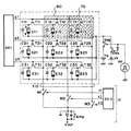
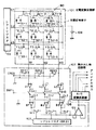
図11において、S11〜S33は光電変換素子で下部電極側をG、上部電極側をDで示している。C11〜C33は蓄積用コンデンサ、T11〜T33は転送用TFTである。Vsは読み出し用電源、Vgはリフレッシュ用電源であり、それぞれスイッチSWs,SWgを介して全光電変換素子S11〜S33のG電極に接続されている。スイッチSWsはインバータを介して、スイッチSWgは直接にリフレッシュ制御回路RFに接続されており、リフレッシュ期間はスイッチSWgがonするよう制御されている。
【0056】
1画素は、1個の光電変換素子とコンデンサ、およびTFTで構成され、その信号出力は信号配線SIGにより検出用集積回路ICに接続されている。以前我々が提案した光電変換装置は計9個の画素を3つのブロックに分け1ブロックあたり3画素の出力を同時に転送しこの信号配線SIGを通して検出用集積回路ICによって順次出力に変換され出力される(Vout)。また1ブロック内の3画素を横方向に配置し、3ブロックを順に縦に配置することにより各画素を2次元的に配置している。
【0057】
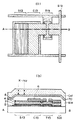
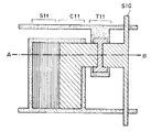
図中破線で囲んだ部分は大面積の同一絶縁基板上に形成されているが、このうち第1画素に相当する部分の模式的平面図を図4に示す。また図中破線A−Bで示した部分の模式的断面図を図5に示す。S11は光電変換素子、T11はTFT、C11はコンデンサ、およびSIGは信号配線である。この光電変換装置においてはコンデンサC11と光電変換素子S11は特別に素子を分離しておらず、光電変換素子S11の電極の面積を大きくすることによりコンデンサC11を形成している。これは光電変換素子とコンデンサが同じ層構成であるから可能なことである。
【0058】
また、画素上部にはパッシベーション用窒化シリコン膜SiNと波長変換体としてのヨウ化セシウム等の蛍光体CsIが形成されている。上方よりX線(X−ray)が入射すると蛍光体CsIにより光電変換素子が感度を有する波長の光(破線矢印)に波長変換され、この光が光電変換素子に入射される。
【0059】
次に図11と図6によって、この光電変換装置の動作の一例について説明する。図6は図11に示される素子の動作を示すタイミングチャートである。
【0060】
はじめにシフトレジスタSR1およびSR2により制御配線g1〜g3、s1〜s3にHiが印加される。すると転送用TFT・T11〜T33とスイッチM1〜M3がonして導通し、全光電変換素子S11〜S33のD電極はGND電位になる(積分検出器Ampの入力端子はGND電位に設計されているため)。同時にリフレッシュ制御回路RFがHiを出力しスイッチSWgがonし全光電変換素子S11〜S33のG電極はリフレッシュ用電源Vgにより正電位になる。すると全光電変換素子S11〜S33はリフレッシュモードになりリフレッシュされる。
【0061】
次に、リフレッシュ制御回路RFがLoを出力しスイッチSWsがonし、全光電変換素子S11〜S33のG電極は読み取り用電源Vsにより負電位になる。すると全光電変換素子S11〜S33は光電変換モードになり同時にコンデンサC11〜C33は初期化される。この状態でシフトレジスタSR1およびSR2により制御配線g1〜g3、s1〜s3にLoが印加される。すると転送用TFT・T11〜T33のスイッチM1〜M3がoffし、全光電変換素子S11〜S33のD電極はDC的にはオープンになるがコンデンサC11〜C33によって電位は保持される。しかしこの時点ではX線は入射されていないため全光電変換素子S11〜S33には光は入射されず光電流は流れない。
【0062】
この状態でX線がパルス的に出射され人体等を通過し蛍光体CsIに入射すると可視光に変換され、その光がそれぞれの光電変換素子S11〜S33に入射する。この光は人体等の内部構造の情報が含まれている。この光により流れた光電流は電荷としてそれぞれのコンデンサC11〜C33に蓄積されX線の入射終了後も保持される。
【0063】
つぎに、シフトレジスタSR1により制御配線g1にHiの制御パルスが印加され、シフトレジスタSR2の制御配線s1〜s3への制御パルス印加によって転送用TFT・T11〜T33のスイッチM1〜M3を通してv1〜v3が順次出力される。同様にシフトレジスタSR1,SR2の制御により他の光信号も順次出力される。これにより人体等の内部構造の2次元情報がv1〜v9として得られる。静止画像を得る場合はここまでの動作であるが動画像を得る場合はここまでの動作を繰り返す。
【0064】
このような光電変換素子を有する光電変換装置では、光電変換素子のG電極が共通に接続され、この共通の配線をスイッチSWgとスイッチSWsを介してリフレッシュ用電源Vgと読み取り用電源Vsの電位に制御している為、全光電変換素子を同時にリフレッシュモードと光電変換モードとに切り換えることができる。このため複雑な制御なくして1画素あたり1個のTFTで光出力を得ることができる。
【0065】
また、このような光電変換素子を有する光電変換装置では、9個の画素を3×3に2次元配置し3画素ずつ同時に、3回に分割して転送・出力したがこれに限らず、例えば縦横1mmあたり5×5個の画素を2000×2000個の画素として2次元的に配置すれば40cm×40cmのX線検出器が得られる。これをX線フィルムの代わりにX線発生器と組み合わせX線レントゲン装置を構成すれば胸部レントゲン検診や乳ガン検診に使用できる。するとフィルムと異なり瞬時にその出力をCRTで映し出すことが可能で、さらに出力をディジタルに変換しコンピュータで画像処理して目的に合わせた出力に変換することも可能である。また光磁気ディスクに保管もでき、過去の画像を瞬時に検索することもできる。また感度もフィルムより良く人体に影響の少ない微弱なX線で鮮明な画像を得ることもできる。
【0066】
図7、図8にたとえば2000×2000個の画素を持つ光電変換装置の実装を示す平面図を示す。2000×2000個の検出器を構成する場合図11で示した破線内の素子を縦・横に数を増やせばよいが、この場合制御配線もg1〜g2000と2000本になり信号配線SIGもsig1〜sig2000と2000本になる。またシフトレジスタSR1や検出用集積回路ICも2000本の制御・処理をしなければならず大規模となる。これをそれぞれ1チップの素子で行なうことは1チップが非常に大きくなり製造時の歩留まりや価格等で不利である。そこで、シフトレジスタSR1は例えば100段ごと1個のチップに形成し、20個(SR1−1〜SR1−20)を使用すれば良い。また検出用集積回路も100個の処理回路ごと1個のチップに形成し、20個(IC1〜IC20)を使用する。
【0067】
図7には、左側(L)に20チップ(SR1−1〜SR1−20)と下側(D)に20チップ実装し、1チップあたり100本の制御配線、信号配線を各々ワイヤーボンディングでチップと接線している。図7中破線部は図11の破線部に相当する。また外部への接続は省略している。また、SWg,SWs,Vg,Vs,RF等も省略している。検出用集積回路IC1〜IC20からは20本の出力(Vout)があるが、これらはスイッチ等を介して1本にまとめたり、20本をそのまま出力し並列処理すればよい。
【0068】
図8には、別の例を示す。左側(L)に10チップ(SR1−1〜SR1−10)と右側(R)に10チップ(SR1−11〜SR1−20)と上側(U)に10チップ(IC1〜10)、下側(D)に10チップ(IC11〜20)を実装している。この構成は上・下・左・右側(U、D、L、R)にそれぞれ各配線を1000本ずつに振り分けているため、各辺の配線の密度が小さくなり、また各辺のワイヤーボンディングの密度も小さく、歩留まりが向上する。配線の振り分けは左側(L)にg1,g3,g5,…g1999、右側(R)にg2,g4,g6,…g2000とし、つまり奇数番目の制御線を左側(L)、偶数番目の制御線を右側(R)に振り分ける。こうすると各配線は等間隔に引き出され配線されるので密度の集中なく歩留まりが向上する。また、上側(U)下側(D)への配線も同様に振り分ければよい。
【0069】
また、図示していないが、別の例として配線の振り分けは左側(L)にg1〜g100,g201〜g300,…g1801〜g1900、右側(R)にg101〜g200,g301〜g400,…g1901〜g2000を振り分け、つまり、1チップごと連続な制御線を振り分け、これを左・右側(L・R)交互に振り分ける。こうすると、1チップ内は連続に制御でき、駆動タイミングが楽で回路を複雑にしなくてよく安価なものが使用できる上・下側(U・D)についても同様で、連続な処理が可能で安価な回路が使用できる。
【0070】
また図7及び図9共に1枚の基板上に破線部の回路を形成した後、その基板上にチップを実装してもよいし、別の大きな基板上に破線部の回路基板とチップを実装してもよい。また、チップをフレキシブル基板上に実装して破線部の回路基板に貼り付け接続してもよい。
【0071】
またこのような非常に多くの画素をもつ大面積の光電変換装置は従来の光センサを用いた複雑な工程では不可能であったが、以前我々が提案した光電変換装置の工程は各素子を共通な膜で同時に形成しているため工程数が少なく、簡易的な工程ですむため高歩留まりが可能で低コストで大面積・高性能の光電変換装置の生産を可能としている。また、コンデンサ及びTFTと光電変換素子とが同じ画素内で構成でき、実質上素子を半減することが可能でさらに歩留まりを向上できる。
【0072】
以上説明したように、図4に示した構成の光電変換素子を有する光電変換装置によれば光電変換装置内の光電変換素子は注入阻止層が一カ所のみで光の入射量を検出することができ、プロセスの最適化が容易で、歩留まりの向上が図れ、製造コストの低減が可能で、SN比の高い低コストの光電変換装置を提供することができる。
【0073】
また、第一の電極層/絶縁層/光電変換半導体層においてトンネル効果や、ショットキーバリアを利用していないため、電極材料は自由に選択でき、絶縁層の厚さやその他の制御も自由度が高い。
【0074】
また、同時に形成する薄膜電界効果トランジスタ(TFT)等のスイッチ素子または/および容量素子とはマッチングが良く、同一膜構成のため共通な膜として同時に形成可能でかつ光電変換素子、TFT共に重要な膜構成は同一真空内で同時に形成可能であり、さらに光電変換装置を高SN比、低コスト化することができる。
【0075】
また、コンデンサも中間層に絶縁層を含んでおり、良好な特性で形成でき複数の光電変換素子で得られた光情報の積分値を簡単な構成で出力できる高機能の光電変換装置が提供できる。
【0076】
また、低コストで大面積・高機能・高特性のファクシミリやX線レントゲン装置を提供できる。
【0077】
本発明ではこのような光電変換素子を用いて構成された光電変換装置において、X線を光電変換素子が感知できる波長域に波長変換することができる蛍光体のような波長変換体を用いることでX線を検出することができる光電変換装置とすることができる。
【0078】
そして、本発明では、光電変換素子に対応して遮へい部材を設けている。
【0079】
それによって本発明は光電変換装置とは別に補正用の光電変換装置を別個に設ける必要がなくなり、それにともなう補正用の回路を光電変換装置の駆動用回路と独立して別個に設けることが不要になる。
【0080】
従って、本発明によれば安定した読取りを行なうことができる光電変換装置を低コストかつ高歩留まりで提供することができる。
【0081】
以下、本発明の実施形態を、図面に基づいて詳細に説明する。
【0082】
(第1の実施形態)
図1は、光電変換装置の概略的回路図である。
【0083】
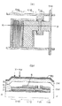
ここで、光電変換装置の回路図は、図11と基本的に同じである。異なる点は、光電変換素子S11〜S13を信号出力補正用の素子として用いる点である。具体的には、光電変換素子S13上に光透過率がゼロである遮光物(遮光フィルタ)70と光電変換素子S12上に光透過率が50%である遮光物(遮光フィルタ)80を配置している点である。
【0084】
図2(a)及び図2(b)は、C13,T13,S13の一例を説明する模式的平面図及び模式的断面図であり、図4で説明したものと基本的に同じである。異なる点は、C13,T13,S13上のCsIとSiNの間に光透過率がゼロである遮光物(遮光フィルタ)70が配置されている点である。
【0085】
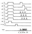
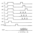
図3は、本実施形態に係る光電変換装置の動作の一例を説明する為のタイミングチャート図である。
【0086】
図3のタイミングチャート図は、光電変換装置上に一様なX線量を照射している場合である。従って、Voutの出力値の内、v1,v4〜v9が、ほぼ同一の出力値となっている。
【0087】
上述したように、光電変換素子S13上に光透過率が略0%である遮光物(遮光フィルタ)70を配置しているため、Voutの出力値の内、v3の出力値はゼロを示している。
【0088】
光電変換素子S12上に光透過率が50%である遮光物(遮光フィルタ)80を配置しているため、v2の出力値はv1,v4〜v9の出力値の50%の出力値になっている。
【0089】
従って、光透過率がゼロである遮光物(遮光フィルタ)70を配置した光電変換素子の出力v3を用いてオフセット補正を行なうことができる。
【0090】
これは、具体的には、オフセット補正用ICに前記光電変換素子の出力V3を入力し、V1,V4〜V9の値からV3の値を差し引くことにより、オフセット補正が行なわれる。
【0091】
また、光透過率が50%である遮光物(遮光フィルタ)80を配置した光電変換素子の出力v2及びフィルタを配置していない光電変換素子の出力として、例えば、v1を用いて感度の補正を行なうことが可能となる。
【0092】
これは、具体的には、感度補正用ICに前記光電変換素子の出力V1,V2の出力値を入力し、V4〜V9の値から、各々V1の値を差し引いた値に50%を乗じた値を用いて感度補正が行なわれる。
【0093】
また、本実施形態では、感度補正用光電変換素子として、光透過率が50%のフィルタを用いたが、これは、50%に限ることはなく、光透過率をmとした場合、0<m<100%のものを用いることが可能となる。
【0094】
(第2の実施形態)図12は、本発明の特徴を示す、第2の実施形態に係る光電変換装置の全体回路図である。
【0095】
ここで、光電変換装置の回路図は、基本的に図11と同じである。本実施例では、光電変換素子S11〜S13を信号出力補正用回路として用いている。具体的には、光電変換素子S12及びS13上に設けられた蛍光体CsI上に、蛍光体CsIへのX線照射量をほぼゼロにできるようにX線透過率がゼロ又はほぼ0の鉛板90を配置している。
【0096】
図13(a)及び図13(b)は、C13,T13,S13の一例を説明するための模式的平面図及び模式的断面図である。本実施例では、C13,T13,S13上のCsIの上部にX線透過率がほぼゼロに出来る鉛板90が配置されている点である。
【0097】
図14は、本発明の第2の実施形態に係る動作を説明する為のタイミングチャート図である。
【0098】
ここで、図14の光電変換装置の回路図のタイミングチャート図では、光電変換装置上に一様なX線量を照射しているため、Voutの出力値の内、v1,v4〜v9が、ほぼ同一の出力値となっている。
【0099】
上述したように、光電変換素子S12及びS13上に蛍光体CsIをはさんでX線透過率が0%であるように鉛板90を配置しているため、Voutの出力値の内、v2及びv3の出力値はゼロを示している。
【0100】
従って、X線透過率がゼロであるようにした鉛板90を配置した光電変換素子の出力v2又はv3を用いてオフセット補正を行なうことができる。
【0101】
これは、具体的には、オフセット補正用ICに前記光電変換素子の出力V2又はV3を入力し、V1,V4〜V9の値からV2又はV3の値を差し引くことにより、オフセット補正が行なわれる。
【0102】
(第3の実施形態)
図15は本発明の第3の実施例を示す光電変換装置の回路図である。説明を簡単化するために、図においては3×3の合計9画素で構成している。S1−1〜S3−3は可視光を受光し電気信号に変換するための光電変換素子であり、T1−1〜T3−3は光電変換素子S1−1〜S3−3で光電変換された信号電荷を、マトリクス信号配線M1〜M3側へ転送するためのスイッチ素子である。G1〜G3はシフトレジスタ(SR1)に接続され且つスイッチ素子T1−1〜T3−3に接続されたスイッチのゲート駆動用配線である。ここで、光電変換装置の回路図では、光電変換素子S1−1〜S3−3を信号出力補正用回路として用いている。具体的には、光電変換素子S1−2及びS1−3上の蛍光体CsI上に、X線透過率がほぼゼロにできるように鉛板90を配置している。マトリクス信号配線M1には、スイッチ素子の電極間容量(Cgs)の3個分の容量が転送時において付加されているが、図中内では容量素子としての表記をしていない。他のマトリクス信号配線M2,M3についても同様である。光電変換素子S1−1〜S3−3とスイッチング素子T1−1〜T3−3とゲート駆動配線G1〜G3とマトリクス信号配線M1〜M3が図中光電変換回路部101内に示されている。光電変換回路部101は絶縁基板上に配置されている。102は駆動用回路部としての、スイッチ素子T1−1〜T3−3を開閉するためのシフトレジスタ(SR1)である。A1〜A3は、マトリクス信号配線M1〜M3の信号電荷を増幅し、インピーダンス変換するためのオペアンプであり、図中においては電圧ホロワ回路を構成したバッファーアンプとしてのみ記載してある。Sn1からSn3はオペアンプA1〜A3の出力すなわち各マトリクス信号配線M1〜M3の出力を読み出し、コンデンサCL1〜CL3へ転送する転送スイッチである。読み出しコンデンサCL1〜CL3は、電圧ホロワ回路を構成したバッファアンプB1〜B3を介して読み出し用スイッチSr1〜Sr3により読み出される。103は読み出し用スイッチSr1〜Sr3を切り替えるためのシフトレジスタ(SR2)である。CL1〜CL3の並列信号は、Sr1〜Sr3とシフトレジスタ(SR2)103により直列変換され、最終段の電圧ホロワ回路を構成したオペアンプ104に入力され、さらにA/D変換回路部105でディジタル化される。RES1〜RES3はマトリクス信号配線M1〜M3に付加された容量(3個分のCgs)に蓄えられた信号成分をリセットするためのリセット用スイッチであり、CRES端子からのパルスにより、あるリセット電位にリセット(図中ではGND電位にリセット)される。また、106は光電変換素子S1−1〜S3−3にバイアスを与えるための電源である。読み出し用回路部107は、バッファアンプA1〜A3、転送スイッチSn1〜Sn3、読み出しコンデンサCL1〜CL3、バッファアンプB1〜B3、読み出し用スイッチSr1〜Sr3、シフトレジスタSR2、最終段のオペアンプ104、リセット用スイッチRES1〜RES3で構成されている。
【0103】
このような回路構成であっても、鉛板によってX線を遮へいしているので、未照射時のオフセット成分を同様に除去することができる。
【0104】
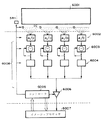
(第4の実施形態)
図16は、本発明の光電変換装置を用いたシステム全体の一例を表す模式的ブロック図である。図16において、6001はセンサ基板である。この図では複数のシフトレジスタSR1を直列に、また検出用集積回路ICも複数で駆動している。検出用集積回路ICの出力は処理回路6008内のアナログ−デジタル変換器6002に入力されデジタル化される。この出力は固定パターン補正用の引き算器6003を介してメモリ6004に記憶される。メモリの中の情報はコントロール6005により制御されバッファ6006を介し信号処理手段としてのイメージプロセッサに転送され、そこで画像処理される。
【0105】
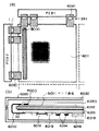
図17(a)、図17(b)は、夫々本発明をX線検出用の光電変換装置に適用した場合の模式的構成図及び模式的断面図である。
【0106】
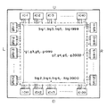
図17において、光電変換素子とTFTの組はセンサ基板6011内に複数個形成され、シフトレジスタSR1又は検出用集積回路ICが実装されたフレキシブル回路基板6010が接続されている。フレキシブル回路基板6010の他方側は回路基板PCB1,PCB2に接続されている。センサ基板6011の複数枚が基台6012の上に接着され大型の光電変換装置を構成する基台6012の下には処理回路6018内のメモリ6014をX線から保護するため鉛板6013が実装されている。センサ基板6011上にはX線光電変換素子が感知できるようなたとえば可視光に変換するための波長変換体としての蛍光体6030(たとえばCsI)が、塗布または貼り付けられている。前述したX線検出方法と同様、X線の照射量に応じた可視光量を検出することでX線を検出することができる。本実施形態では図17(b)に示されるように全体をカーボンファイバー製のケース6020に収納している。
【0107】
ここで、センサ基板6011の左上角に光透過率がゼロである遮光物(遮光フィルタ)7000と光透過率が50%である遮光物(遮光フィルタ)8000が配置してあり、光透過率がゼロである遮光物(遮光フィルタ)7000を配置した光電変換素子の出力を用いオフセット補正を行ない、光透過率が50%である遮光物(遮光フィルタ)8000を配置した光電変換素子の出力及びフィルタを配置していない光電変換素子の出力を用いて感度の補正を行なうことが可能となる。
【0108】
(第5の実施形態)
図18(a)、図18(b)は、夫々本発明をX線検出用の光電変換装置に適用した場合の模式的構成図及び模式的断面図である。
【0109】
図18において、光電変換素子とTFTの組はセンサ基板6011内に複数個形成され、シフトレジスタSR1と検出用集積回路ICが実装されたフレキシブル回路基板6010が接続されている。フレキシブル回路基板6010の他方側は回路基板PCB1,PCB2に接続されている。センサ基板6011の複数枚が基台6012の上に接着され大型の光電変換装置を構成する基台6012の下には処理回路6018内のメモリ6014をX線から保護するため鉛板6013が実装されている。センサ基板6011上には第4の実施形態と同様にX線を可視光に変換するための蛍光体6030たとえばCsIが、塗布または貼り付けられている。
【0110】
本実施形態では図18(b)に示されるように全体をカーボンファイバー製のケース6020に収納している。
【0111】
本例においては、蛍光体6030上にX線を遮断又は実質的に遮断して、蛍光体6030中に入射させないように遮へい部材としての鉛板9000を設けている。鉛板9000に対応する位置に設けられた光電変換素子中には蛍光体6030からの光が入射されないか実質的に入射されない。従って、該光電変換素子からの出力を用いてオフセット補正を行なうことができる。
【0112】
(第6の実施形態)
図19(a)及び図19(b)は夫々本発明をX線検出用の光電変換装置に適用した場合の模式的構成図及び模式的断面図である。
【0113】
本実施形態は遮へい部材としての鉛板9000が、シフトレジスタSR1の接続側端部の光電変換素子上にライン状に配されている以外は第5の実施形態と変わりはない。
【0114】
本実施形態では各シフトレジスタSR1に対応するラインごとにおけるオフセット補正を行なうことができる。したがって、各ラインごとに異なるオフセットを有する場合でも補正可能になり、より一層均質な出力特性を得ることができる。
【0115】
(第7の実施形態)
図20(a)及び図20(b)は夫々本発明をX線検出用の光電変換装置に適用した場合の模式的構成図及び模式的断面図である。
【0116】
本実施形態ではシフトレジスタSR1に接続される側でなく、検出用集積回路用のICが接続された側の端部の光電変換素子上に対応して遮へい部材である鉛板をライン状に設けた点が第6の実施形態と異なる。
【0117】
本実施形態では各出力ラインごとにオフセット補正をすることができるのでより簡便に出力特性の調整を行なうことができる。
【0118】
尚、本実施形態に加えて、第6の実施形態で説明したようにシフトレジスタSR1に沿ってライン状に遮へい部材としての鉛板を設けてもよい。
【0119】
又、第6及び第7の実施形態において、遮へい部材は蛍光体6030の光電変換素子側に設けても良い。この場合はより近いところで光を遮へいするので蛍光体からのまわりこみがより少なくできる。また蛍光体上に遮へい部材を設ける場合は、蛍光体の設置が容易になるとともに蛍光体自身の発光(波長変換)が生じないという効果もある。
【0120】
又、蛍光体と光電変換素子との間に遮へい部材を設ける場合は蛍光体からの発光が遮ぎられればよいのであるから、発光色に対する充分な濃度の補色成分を有すれば黒である必要はない。たとえば発光色が緑色の場合、充分な濃度の赤色フィルター(赤色成分を有するフィルター)であれば良い。
【0121】
つまり、遮へい部材はX線が透過しても蛍光体中での発光又は実質的発光がなければよく、発光があっても光電変換素子が感知できない又は実質的に感知できなければよい。加えて、蛍光体の発光を遮ぎるときは、光電変換素子が感知できない又は実質的に感知できなければよい。
【0122】
加えて、光電変換素子上に鉛板のような遮へい部材を設け、蛍光体をそれに対応する素子上に設けないようにするのも一つの形態である。
【0123】
図21は、本発明の光電変換装置をX線診断システムへ応用した一例を示す、システム構成図である。
【0124】
図21において、X線チューブ6050で発生したX線6060は、患者あるいは被検体6061の検査部6062を透過し、蛍光体を上部に実装した光電変換装置6040に入射する。この入射したX線には被検体6061の内部の情報が含まれている。X線の入射に対応して蛍光体は発光し、これを光電変換して、電気的情報を得る。この情報はディジタルに変換されイメージプロセッサ6070により画像処理され制御室のディスプレイ6080で観察できる。これによって、被検体の被破壊検査を行なうことができる。
【0125】
また、この情報は電話回線6090等の伝送手段により遠隔地へ転送でき、別の場所のディスプレイ6081に表示もしくは光ディスク等の保存手段に保存することができ、遠隔地の医師や検査官が診断することも可能である。またフィルムプロセッサ6100によりフィルム6110に記録することもできる。
【0126】
このように4枚のセンサ基板を貼り合わせて1つの基板として、X線診断システムを構成する場合、光電変換素子の出力値を補正する為の補正用光電変換素子を、該基板の中で比較的重要でない角部又は辺のいずれか、又は4つの角部又は少なくとも2辺に配置する(4隅あるいは対向する2辺の光電変換素子を用いる)ことが可能になり、出力値をスキャンする時間も特別に必要にならない。更に、各センサ基板に最低1つずつの補正用光電変換素子を構成することにより、各センサ基板間のオフセット及び感度の補正を行なうことも可能になる。
【0127】
光電変換装置の隅は、比較的重要な部位ではない為、そこを用いるのが好ましい。パネルを4枚貼り合わせる場合、各パネルの1つの隅にフィルタのような遮へい部材を配置すると、各パネル毎のバラツキも補正することが可能となる。
【0128】
また、図17に示す0%フィルター7000と50%フィルター8000は、図17に示すような形状に配置することにより、入射光の反射光、及びその他のもれ光の影響を少なくすることができ、光のクロクトークの影響を減少することができるものである。
【0129】
【発明の効果】
以上説明したように、本出願に係る発明によれば、基板上に2次元的に配列された複数の光電変換素子を、X方向の駆動線を順次スキャンし、Y方向の信号線に信号電荷を転送し、順次信号を読み出す光電変換装置に於いて、任意の光電変換素子上に光透過率が略ゼロであるフィルタもしくは、任意の光電変換素子上に、X線透過率がゼロとできる鉛板に代表される遮へい部材を配置することにより、その任意の光電変換素子をオフセット出力補正用の光電変換素子として用いることができるため、別に、補正用光電変換素子を形成する必要がなくなる。
【0130】
その結果、外部の補正用光電変換素子の出力を補正用ICに入力する為の接続回路及びその作業が不要となり、歩留まりの向上及びコストの低減が可能になる。
【0131】
また、前記光電変換装置に於いて、任意の光電変換素子上に光透過率mが0<m<100%であるフィルタを配置することにより、感度補正用光電変換素子として用いることが可能となり、別に補正用光電変換素子を形成する必要が無くなる。
【0132】
また、これらの補正用光電変換素子を用いることにより、光電変換素子の照度に対する感度や、照度ゼロ時における出力即ちオフセット出力値のばらつきをなくすことが可能となる。
【0133】
また、補正回路を光電変換装置上に独立に配置する場合と異なり、回路が煩雑にならず、光電変換装置を作成する上で歩留まりを下げることもなく、コストを上げることにつながらないという効果が得られる。
【0134】
更に、本実施形態のように、多画素で構成された2次元の光電変換装置の中の一部の光電変換素子を補正用光電変換素子として用いる場合、補正用光電変換素子を光電変換装置上に独立に配置する場合と異なり、補正出力を読み出す時間が余分に必要とならず、結果的に光電変換素子の出力値を補正することを短時間で行なうことが可能となり、動画像を得ることが容易に可能となる。
【0135】
また、k枚(たとえば4枚)のセンサ基板を貼り合わせて1つの基板を得る場合は、X線診断システムなどを構成する場合、光電変換素子の出力値を補正する為の補正用光電変換素子を、基板の中で比較的重要でない角又は辺に配置することが可能になり、出力値をスキャンする時間も特に必要にならない。
【0136】
更に、各センサ基板に最低1つずつの補正用光電変換素子を構成することにより、各センサ基板間のオフセット及び/又は感度の補正を行なうことも可能になる。
【0137】
尚、本発明は本発明の主旨の範囲内において適宜、変形組合せが可能である。
【図面の簡単な説明】
【図1】図1は本発明の光電変換装置の一例を説明するための概略的回路図である。
【図2】図2(a)は本発明の光電変換装置の補正用光電変換素子の一例を説明するための模式的平面図、(b)は図2(a)に示される補正用の光電変換素子の模式的断面図である。
【図3】図3は本発明の光電変換装置の駆動の一例を説明するためのタイミングチャートである。
【図4】図4は図11の光電変換部の一画素構成の一例を示す模式的平面図である。
【図5】図5は図11の光電変換部の一画素構成の一例を示す模式的断面図である。
【図6】図6は図11の光電変換装置の駆動の一例を示すタイミングチャートである。
【図7】図7は光電変換装置の実装の一例を示す概略的平面図である。
【図8】図8は光電変換装置の実装の一例を示す概略的平面図である。
【図9】図9(a)及び(b)は夫々光センサの一例を説明するための模式的断面図、(c)は駆動方法の一例を説明するための概略的回路図である。
【図10】図10はTFTの構成の一例を説明するための模式的断面図である。
【図11】図11は光電変換装置の回路構成の一例を示す概略的回路図である。
【図12】図12は本発明の光電変換装置の一例を説明するための概略的回路図である。
【図13】図13(a)は本発明の光電変換装置の補正用光電変換素子の一例を説明するための模式的平面図、図13(b)は図13(a)に示される補正用の光電変換素子の模式的断面図である。
【図14】図14は本発明の光電変換装置の駆動の一例を説明するためのタイミングチャートである。
【図15】図15は本発明の光電変換装置の一例を説明するための概略的回路図である。
【図16】図16は本発明の光電変換装置の一例を説明するための概略的回路図である。
【図17】図17(a)は本発明の一例としての実施形態の光電変換装置を説明するための模式的平面図、(b)は模式的断面図である。
【図18】図18(a)は本発明の一例としての実施形態の光電変換装置を説明するための模式的平面図、(b)は模式的断面図である。
【図19】図19(a)は本発明の一例としての実施形態の光電変換装置を説明するための模式的平面図、(b)は模式的断面図である。
【図20】図20(a)は本発明の光電変換装置の構成の一例を示す模式的平面図、(b)は模式的断面図である。
【図21】図21は本発明の光電変換装置を有するX線診断(検査)システムの一例を説明するための概略的システム構成図である。
【符号の説明】
70 光透過率0%の遮光フィルタ
80 光透過率50%の遮光フィルタ
S11〜533 光電変換素子
T11〜T33 転送用TFT
C11〜C33 コンデンサ
SR1,SR2 シフトレジスタ[0001]
BACKGROUND OF THE INVENTION
The present invention relates to a photoelectric conversion device, and more particularly to a photoelectric conversion device in which a plurality of photoelectric conversion elements capable of obtaining a reference signal for signal correction are arranged.
[0002]
[Prior art]
In a photoelectric conversion device in which a plurality of photoelectric conversion elements are arranged, the output (in other words, sensitivity) or irradiation when the light receiving region where the photoelectric conversion elements are arranged is irradiated as compared with each device. In general, there is some variation in the value of output (that is, offset output) when there is no (zero irradiation). Such output variations are preferably corrected in order to bring out the full performance of the photoelectric conversion device. Therefore, a correction circuit for correcting variations and a photoelectric conversion element for correction for obtaining an output used for correction are generally provided.
[0003]
Such an offset correction circuit and a sensitivity correction circuit are commercially available as “correction ICs”. However, a special photoelectric conversion element for taking in correction data to be input to such a correction IC has been used. That is, the offset value correcting photoelectric conversion element is generally provided independently on the photoelectric conversion device. Specifically, a CCD sensor made of, for example, crystalline silicon is disposed outside the light receiving portion of the photoelectric conversion device, and the output value at the time of zero illuminance is monitored and used as correction data.
[0004]
Similarly to the case of the offset value correcting photoelectric conversion element, the sensitivity correcting photoelectric conversion element is also placed outside the light receiving portion of the photoelectric conversion device, for example, with a filter on a CCD sensor made of crystalline silicon. Then, an arbitrary value between 0 and 100% in illuminance is monitored, and the value is connected to a general correction circuit to correct data actually read by the photoelectric conversion device.
[0005]
[Problems to be solved by the invention]
However, when such a photoelectric conversion element for correction is arranged independently on the photoelectric conversion device, a circuit for reading out the output value of the photoelectric conversion element for correction becomes complicated, and the yield is lowered in creating the photoelectric conversion device, There was a problem that led to an increase in cost.
[0006]
Furthermore, when configuring a two-dimensional photoelectric conversion device composed of multiple pixels, if a circuit for reading the output value of the correction photoelectric conversion element is arranged independently on the photoelectric conversion device, it takes extra time to read the correction output. Therefore, as a result, the output value of the photoelectric conversion element cannot be corrected in a short time, and there is a problem that it may be an obstacle to obtain a moving image.
[0007]
[Object of invention]
An object of the present invention is to realize means capable of correcting an offset output value without being arranged independently in a photoelectric conversion element for obtaining an offset correction output value and a sensitivity correction output value.
[0008]
It is also intended to realize a photoelectric conversion device that can improve the yield, reduce the cost, shorten the correction output read time, and easily obtain a moving image.
[0009]
Another object of the present invention is to provide a photoelectric conversion device having a configuration capable of correcting variations in output in rows and / or columns in a photoelectric conversion device arranged in a matrix (two-dimensional). .
[0010]
In addition, the present invention provides a photoelectric conversion device including a photoelectric conversion unit having a plurality of photoelectric conversion elements arranged two-dimensionally on a substrate. It is an object of the present invention to provide a photoelectric conversion device in which a shielding member having a transmittance or light transmittance of 0% or substantially 0% is disposed on the X-ray or light incident side of the photoelectric conversion element.
[0011]
[Means for Solving the Problems]
The present invention provides, as means for solving the above problems, a photoelectric conversion unit having a plurality of photoelectric conversion elements arranged two-dimensionally on a substrate, and a photoelectric conversion unit provided on the photoelectric conversion unit. , X-rays are converted into light having a wavelength with which the photoelectric conversion element has sensitivity. In a photoelectric conversion device comprising a wavelength converter, Of the plurality of photoelectric conversion elements Compatible with any photoelectric conversion element Light An offset correction output value output from the arbitrary photoelectric conversion element by arranging a shielding member having a transmittance of 0% or substantially 0% between the arbitrary photoelectric conversion element and the wavelength converter. And an output value output from the plurality of photoelectric conversion elements excluding the arbitrary photoelectric conversion element, to provide offset correction.
[0012]
The shielding member is Shading It is also a photoelectric conversion device including a filter.
[0013]
Also, the Shading The filter Shading It is also a photoelectric conversion device characterized by having a component of a complementary color relationship with light incident on the filter.
[0014]
Furthermore, Between any other photoelectric conversion elements of the plurality of photoelectric conversion elements and the wavelength converter, It is also a photoelectric conversion device characterized by having a second shielding member having a light transmittance m of 0 <m <100%.
[0015]
The photoelectric conversion element corresponding to the shielding member is offset It is also a photoelectric conversion device characterized by being a photoelectric conversion element for correction.
[0016]
The photoelectric conversion device corresponding to the second shielding member is a photoelectric conversion device for correcting sensitivity, and is also a photoelectric conversion device.
[0017]
The shielding member is arranged corresponding to the photoelectric conversion element located at the corner of the photoelectric conversion unit. Place It is also a photoelectric conversion device that is characterized by the above.
[0018]
The shielding member is arranged corresponding to the row of the photoelectric conversion elements. Place It is also a photoelectric conversion device that is characterized by the above.
[0019]
In addition, the photoelectric conversion element column includes a column at an end of the photoelectric conversion unit.
[0023]
The wavelength converter is also a photoelectric conversion device characterized in that it contains a phosphor.
[0024]
Also, The output value for sensitivity correction output from the other arbitrary photoelectric conversion element in which the second shielding member is disposed correspondingly, and the arbitrary photoelectric conversion element and the other arbitrary photoelectric conversion element are excluded. And a sensitivity correction IC that performs sensitivity correction using output values output from the plurality of photoelectric conversion elements. It is also a photoelectric conversion device characterized by this.
[0025]
Also, An offset correction IC for performing the offset correction is further included. It is also a photoelectric conversion device characterized by this.
[0026]
The shielding member is lead Is a board It is also a photoelectric conversion device characterized by this.
[0035]
[Action]
In the photoelectric conversion device of the present invention, a photoelectric conversion element for obtaining an output value for correction is provided by providing a shielding member for shielding light carrying information on an element having the same structure adjacent to a photoelectric conversion element for reading information. A conversion element is used. By using the output from the photoelectric conversion element for correction, it becomes unnecessary to provide a photoelectric conversion element for correction independent of the photoelectric conversion device, and more accurate correction can be performed more easily. .
[0036]
In the photoelectric conversion device, a photoelectric conversion element for sensitivity correction and an output value thereof are read out by disposing a filter having a light transmittance m of 0 <m <100% on an arbitrary photoelectric conversion element. It can be used as a circuit.
[0037]
DETAILED DESCRIPTION OF THE INVENTION
Hereinafter, an optical sensor applicable to the present invention will be described.
[0038]
FIGS. 9A to 9C are diagrams illustrating an example of the configuration of the optical sensor, and FIGS. 9A and 9B illustrate the layer configuration of two types of optical sensors. 9 (c) shows a common typical driving method. FIGS. 9A and 9B are both photo-diode type optical sensors. FIG. 9A is called a PIN type, and FIG. 9B is called a Schottky type.
[0039]
9A and 9B, 1 is an insulating substrate, 2 is a lower electrode, 3 is a p-type semiconductor layer (hereinafter referred to as p layer), and 4 is an intrinsic semiconductor layer (hereinafter referred to as i layer). 5 is an n-type semiconductor layer (hereinafter referred to as n layer), and 6 is a transparent electrode.
[0040]
In the Schottky type of FIG. 9B, the material of the
[0041]
In FIG. 9C,
[0042]
The operation will be briefly described here. As shown in FIGS. 9A and 9B, when light enters from the direction indicated by the arrow and reaches the
[0043]
However, there is room for improvement in producing a photoelectric conversion device with a higher SN ratio and lower cost with the above-described optical sensor structure.
[0044]
The first reason is that the PIN type shown in FIG. 9A and the Schottky type shown in FIG. 9B both require two injection blocking layers. In the PIN type of FIG. 9A, the
[0045]
Usually, in order to improve this characteristic, it is necessary to optimize the conditions for forming the
[0046]
The same applies to the Schottky type shown in FIG. In the Schottky type shown in FIG. 9B, a Schottky barrier layer is used for one of the injection blocking layers, and this uses the work function difference between the
[0047]
Also, the need for two injection blocking layers reduces productivity and increases costs. This is because the injection blocking layer is important in terms of characteristics, and if a defect occurs due to dust or the like in one of the two places, there is a possibility that the characteristics as the optical sensor cannot be obtained.
[0048]
The second reason will be described with reference to FIG. FIG. 10 shows a layer structure of a field effect transistor (TFT) formed of a thin semiconductor film. The TFT may be used as a part of the control unit in forming the photoelectric conversion device. In the figure, the same elements as those in FIG. 9 are denoted by the same reference numerals.
[0049]
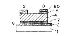
In FIG. 10, 7 is a gate insulating film, and 60 is an upper electrode. The formation method will be described step by step. A
[0050]
When the above-mentioned optical sensor is formed on the same substrate as this TFT, this layer structure becomes a problem, which may lead to an increase in cost and a decrease in characteristics. This is because the configuration of the photosensor shown in FIG. 9 is that the PIN type in FIG. 9A is the substrate / electrode / p layer / i layer / n layer / electrode, and the Schottky type in FIG. 9B is the substrate. This is because the TFT has a configuration of substrate / electrode / insulating film / i layer / n layer / electrode, whereas the configuration is / electrode / i layer / n layer / electrode. This indicates that the sensor and the TFT cannot be formed in the same process, which may lead to a decrease in yield and an increase in cost due to a complicated process. Further, in order to make the i layer / n layer common, an etching process of the
[0051]
Further, in order to improve the Schottky characteristics of FIG. 9B described above, an oxide film or a nitride film formed between the
[0052]
Furthermore, although not shown, a capacitive element (hereinafter referred to as a capacitor), which is an element necessary for obtaining an integrated value of electric charge and current, has the same configuration as the above-mentioned optical sensor and has good characteristics with little leakage. Making things has room for improvement. Since the capacitor is intended to store electric charge between two electrodes, the intermediate layer between the electrodes must always have a layer that prevents the movement of electrons and holes, whereas the above-mentioned photosensor is a semiconductor between the electrodes. This is because it is difficult to obtain an intermediate layer having good characteristics with little thermal leakage since only the layer is used.
[0053]
In this way, TFTs and capacitors, which are important elements for constructing a photoelectric conversion device, are not good in matching in terms of process or characteristics. Many optical sensors are arranged two-dimensionally, and these optical signals are sequentially transmitted. Since the process is complicated and complicated in constructing the entire system to be detected, the yield may be very bad, and it may become a serious problem in making a high-performance multifunctional device at low cost. .
[0054]
FIG. 11 is a schematic overall circuit diagram showing a photoelectric conversion device that can solve the problem of the above-mentioned photosensor, FIG. 4A is a schematic plan view of each component corresponding to one pixel of the photoelectric conversion device, FIG. 4B is a schematic cross-sectional view taken along the line AB of FIG.
[0055]
In FIG. 11, S11 to S33 are photoelectric conversion elements, and the lower electrode side is indicated by G and the upper electrode side is indicated by D. C11 to C33 are storage capacitors, and T11 to T33 are transfer TFTs. Vs is a power source for reading and Vg is a power source for refreshing, which are connected to the G electrodes of all the photoelectric conversion elements S11 to S33 via switches SWs and SWg, respectively. The switch SWs is directly connected to the refresh control circuit RF via the inverter, and the switch SWg is controlled to be turned on during the refresh period.
[0056]
One pixel is composed of one photoelectric conversion element, a capacitor, and a TFT, and the signal output is connected to the detection integrated circuit IC by a signal wiring SIG. The photoelectric conversion device that we proposed before divided 9 pixels into 3 blocks and transferred the output of 3 pixels per block at the same time, and through this signal wiring SIG, it is converted into output sequentially by the detection integrated circuit IC and outputted (Vout). Each pixel is arranged two-dimensionally by arranging three pixels in one block in the horizontal direction and arranging the three blocks in the vertical direction in order.
[0057]
The portion surrounded by the broken line in the drawing is formed on the same insulating substrate having a large area. FIG. 4 shows a schematic plan view of the portion corresponding to the first pixel. FIG. 5 shows a schematic cross-sectional view of a portion indicated by a broken line AB in the drawing. S11 is a photoelectric conversion element, T11 is a TFT, C11 is a capacitor, and SIG is a signal wiring. In this photoelectric conversion device, the capacitor C11 and the photoelectric conversion element S11 are not specially separated, and the capacitor C11 is formed by increasing the area of the electrode of the photoelectric conversion element S11. This is possible because the photoelectric conversion element and the capacitor have the same layer structure.
[0058]
Further, a passivation silicon nitride film SiN and a phosphor CsI such as cesium iodide as a wavelength converter are formed on the top of the pixel. When X-rays enter from above, the phosphor CsI converts the wavelength of the photoelectric conversion element into light having a sensitivity (dashed arrow), and this light enters the photoelectric conversion element.
[0059]
Next, an example of the operation of this photoelectric conversion device will be described with reference to FIGS. 6 is a diagram. 11 5 is a timing chart showing the operation of the element shown in FIG.
[0060]
First, the control wirings g1 to g3 and s1 to s are controlled by the shift registers SR1 and SR2. 3 Hi is applied to. Then, the transfer TFTs T11 to T33 and the switches M1 to M3 are turned on, and the D electrodes of all the photoelectric conversion elements S11 to S33 are set to the GND potential (the input terminal of the integration detector Amp is designed to the GND potential). Because). At the same time, the refresh control circuit RF outputs Hi, the switch SWg is turned on, and the G electrodes of all the photoelectric conversion elements S11 to S33 are set to a positive potential by the refresh power supply Vg. Then, all the photoelectric conversion elements S11 to S33 enter the refresh mode and are refreshed.
[0061]
Next, the refresh control circuit RF outputs Lo, the switch SWs is turned on, and the G electrodes of all the photoelectric conversion elements S11 to S33 are set to a negative potential by the reading power source Vs. Then, all the photoelectric conversion elements S11 to S33 enter the photoelectric conversion mode, and the capacitors C11 to C33 are initialized at the same time. In this state, the control lines g1 to g3 and s1 to s are controlled by the shift registers SR1 and SR2. 3 Lo is applied to. Then, the switches M1 to M3 of the transfer TFTs T11 to T33 are turned off, and the D electrodes of all the photoelectric conversion elements S11 to S33 are opened in terms of DC, but the potential is held by the capacitors C11 to C33. However, since no X-rays are incident at this time, no light enters the photoelectric conversion elements S11 to S33 and no photocurrent flows.
[0062]
In this state, X-rays are emitted in pulses, pass through the human body, etc., and enter the phosphor CsI, which is converted into visible light, and the light enters each of the photoelectric conversion elements S11 to S33. This light contains information on the internal structure of the human body and the like. The photocurrent flowing by this light is accumulated in each of the capacitors C11 to C33 as electric charges and is held even after the X-ray incidence is completed.
[0063]
Next, a Hi control pulse is applied to the control wiring g1 by the shift register SR1, and v1 to v3 through the switches M1 to M3 of the transfer TFTs T11 to T33 by applying control pulses to the control wirings s1 to s3 of the shift register SR2. Are output sequentially. Similarly, other optical signals are sequentially output under the control of the shift registers SR1 and SR2. Thereby, the two-dimensional information of the internal structure of the human body or the like is obtained as v1 to v9. The operation so far is performed when a still image is obtained, but the operation so far is repeated when a moving image is obtained.
[0064]
In the photoelectric conversion device having such a photoelectric conversion element, the G electrodes of the photoelectric conversion elements are connected in common, and the common wiring is connected to the potentials of the refresh power supply Vg and the read power supply Vs via the switches SWg and SWs. Since it is controlled, all the photoelectric conversion elements can be simultaneously switched between the refresh mode and the photoelectric conversion mode. Therefore, light output can be obtained with one TFT per pixel without complicated control.
[0065]
Moreover, in the photoelectric conversion device having such a photoelectric conversion element, nine pixels are two-dimensionally arranged in 3 × 3, and three pixels are divided and transferred and output at the same time three times. If 5 × 5 pixels per 1 mm in length and width are two-dimensionally arranged as 2000 × 2000 pixels, an X-ray detector of 40 cm × 40 cm can be obtained. If this is combined with an X-ray generator instead of an X-ray film to constitute an X-ray X-ray apparatus, it can be used for chest X-ray screening and breast cancer screening. Then, unlike film, the output can be instantaneously displayed on a CRT, and further, the output can be converted to digital and converted into an output suitable for the purpose by computer processing. It can also be stored on a magneto-optical disk, and past images can be retrieved instantly. It is also possible to obtain a clear image with weak X-rays that have better sensitivity than films and have little effect on the human body.
[0066]
7 and 8 are plan views showing the implementation of a photoelectric conversion device having, for example, 2000 × 2000 pixels. In the case of configuring 2000 × 2000 detectors, the number of elements in the broken line shown in FIG. 11 may be increased vertically and horizontally. In this case, the number of control wirings is g1 to g2000 and 2000, and the signal wiring SIG is also sig1. ~ Sig2000 and 2000. Also, the shift register SR1 and the detection integrated circuit IC have to be controlled and processed in 2000, so the scale becomes large. It is disadvantageous in terms of production yield, price, etc., that each of these is performed with a single chip element, since one chip becomes very large. Therefore, for example, the shift register SR1 may be formed in one chip every 100 stages, and 20 (SR1-1 to SR1-20) may be used. The integrated circuit for detection is also formed on one chip for every 100 processing circuits, and 20 (IC1 to IC20) are used.
[0067]
In FIG. 7, 20 chips (SR1-1 to SR1-20) are mounted on the left side (L) and 20 chips are mounted on the lower side (D), and 100 control wirings and signal wirings per chip are each formed by wire bonding. Is tangent. 7 corresponds to the broken line portion in FIG. Connection to the outside is omitted. SWg, SWs, Vg, Vs, RF, etc. are also omitted. There are 20 outputs (Vout) from the detection integrated circuits IC1 to IC20, but these may be combined into one via a switch or the like, or 20 may be output as they are and processed in parallel.
[0068]
FIG. 8 shows another example. 10 chips (SR1-1 to SR1-10) on the left side (L), 10 chips (SR1-11 to SR1-20) on the right side (R), 10 chips (IC1 to 10) on the upper side (U), lower side ( D) 10 chips (
[0069]
Although not shown, as another example, the distribution of wirings is g1 to g100, g201 to g300,... G1801 to g1900 on the left side (L), and g101 to g200, g301 to g400,. g2000 is distributed, that is, a continuous control line is distributed for each chip, and left and right (LR) are alternately distributed. In this way, one chip can be controlled continuously, the drive timing is easy, and it is possible to use inexpensive ones that do not require complicated circuits. The same applies to the upper and lower sides (UD), and continuous processing is possible. An inexpensive circuit can be used.
[0070]
7 and 9, after forming the broken line circuit on one substrate, the chip may be mounted on the substrate, or the broken line circuit board and the chip may be mounted on another large substrate. May be. Alternatively, the chip may be mounted on a flexible substrate and attached to the circuit substrate at the broken line.
[0071]
In addition, such a large-area photoelectric conversion device having a large number of pixels was impossible in a complicated process using a conventional photosensor, but the process of the photoelectric conversion device that we previously proposed Since a common film is formed at the same time, the number of processes is small and a simple process is required, so that a high yield is possible, and a large area and high performance photoelectric conversion device can be produced at low cost. In addition, the capacitor, the TFT, and the photoelectric conversion element can be configured in the same pixel, so that the element can be substantially halved and the yield can be further improved.
[0072]
As described above, according to the photoelectric conversion device having the photoelectric conversion element having the configuration shown in FIG. 4, the photoelectric conversion element in the photoelectric conversion device can detect the amount of incident light with only one injection blocking layer. In addition, the process can be easily optimized, the yield can be improved, the manufacturing cost can be reduced, and a low-cost photoelectric conversion device with a high SN ratio can be provided.
[0073]
In addition, since the tunnel effect and Schottky barrier are not used in the first electrode layer / insulating layer / photoelectric conversion semiconductor layer, the electrode material can be freely selected, and the thickness of the insulating layer and other controls are also flexible. high.
[0074]
In addition, it has good matching with switching elements such as thin film field effect transistors (TFT) or / and capacitive elements formed at the same time, and can be formed simultaneously as a common film because of the same film configuration, and is an important film for both photoelectric conversion elements and TFTs The structure can be formed simultaneously in the same vacuum, and the photoelectric conversion device can have a high SN ratio and low cost.
[0075]
In addition, the capacitor also includes an insulating layer in the intermediate layer, and can provide a high-performance photoelectric conversion device that can be formed with good characteristics and can output an integrated value of optical information obtained by a plurality of photoelectric conversion elements with a simple configuration. .
[0076]
In addition, it is possible to provide a facsimile and an X-ray X-ray apparatus having a large area, high function, and high characteristics at low cost.
[0077]
In the present invention, in a photoelectric conversion device configured using such a photoelectric conversion element, a wavelength converter such as a phosphor capable of converting the wavelength of X-rays into a wavelength range that can be sensed by the photoelectric conversion element is used. A photoelectric conversion device that can detect X-rays can be obtained.
[0078]
And in this invention, the shielding member is provided corresponding to the photoelectric conversion element.
[0079]
Accordingly, the present invention eliminates the need to separately provide a correction photoelectric conversion device separately from the photoelectric conversion device, and eliminates the need for providing a correction circuit separately from the photoelectric conversion device drive circuit. Become.
[0080]
Therefore, according to the present invention, a photoelectric conversion device capable of performing stable reading can be provided at a low cost and with a high yield.
[0081]
Hereinafter, embodiments of the present invention will be described in detail with reference to the drawings.
[0082]
(First embodiment)
FIG. 1 is a schematic circuit diagram of a photoelectric conversion device.
[0083]
Here, the circuit diagram of the photoelectric conversion device is basically the same as FIG. The difference is that the photoelectric conversion elements S11 to S13 are used as signal output correction elements. Specifically, a light shielding object (light shielding filter) 70 having a light transmittance of zero is disposed on the photoelectric conversion element S13, and a light shielding object (light shielding filter) 80 having a light transmittance of 50% is disposed on the photoelectric conversion element S12. It is a point.
[0084]
2A and 2B are a schematic plan view and a schematic cross-sectional view illustrating an example of C13, T13, and S13, which are basically the same as those described in FIG. A different point is that a light shielding object (light shielding filter) 70 having a light transmittance of zero is arranged between CsI and SiN on C13, T13, and S13.
[0085]
FIG. 3 is a timing chart for explaining an example of the operation of the photoelectric conversion apparatus according to this embodiment.
[0086]
The timing chart of FIG. 3 shows a case where a uniform X-ray dose is irradiated on the photoelectric conversion device. Accordingly, among the output values of Vout, v1, v4 to v9 are substantially the same output value.
[0087]
As described above, since the light shielding object (light shielding filter) 70 having a light transmittance of approximately 0% is disposed on the photoelectric conversion element S13, the output value of v3 indicates zero among the output values of Vout. Yes.
[0088]
Since the light shielding object (light shielding filter) 80 having a light transmittance of 50% is arranged on the photoelectric conversion element S12, the output value of v2 is 50% of the output values of v1, v4 to v9. Yes.
[0089]
Accordingly, the offset correction can be performed using the output v3 of the photoelectric conversion element in which the light shielding material (light shielding filter) 70 having a light transmittance of zero is arranged.
[0090]
Specifically, the offset correction is performed by inputting the output V3 of the photoelectric conversion element to the offset correction IC and subtracting the value of V3 from the values of V1, V4 to V9.
[0091]
Further, for example, v1 is used to correct the sensitivity as the output v2 of the photoelectric conversion element in which the light shielding member (light shielding filter) 80 having a light transmittance of 50% is disposed and the output of the photoelectric conversion element in which no filter is disposed. Can be performed.
[0092]
Specifically, the output values of the photoelectric conversion elements V1 and V2 are input to the sensitivity correction IC, and the value obtained by subtracting the value of V1 from the values of V4 to V9 is multiplied by 50%. Sensitivity correction is performed using the value.
[0093]
In this embodiment, a filter with a light transmittance of 50% is used as the photoelectric conversion element for sensitivity correction. However, this is not limited to 50%. When the light transmittance is m, 0 < Those with m <100% can be used.
[0094]
(Second embodiment) 12 These are the whole circuit diagrams of the photoelectric conversion apparatus which concerns on 2nd Embodiment which show the characteristics of this invention.
[0095]
Here, the circuit diagram of the photoelectric conversion device is basically the same as FIG. In the present embodiment, the photoelectric conversion elements S11 to S13 are used as signal output correction circuits. Specifically, on the phosphor CsI provided on the photoelectric conversion elements S12 and S13, a lead plate having zero or almost zero X-ray transmittance so that the amount of X-ray irradiation to the phosphor CsI can be made almost zero. 90 is arranged.
[0096]
FIGS. 13A and 13B are a schematic plan view and a schematic cross-sectional view for explaining an example of C13, T13, and S13. In the present embodiment, a
[0097]
FIG. 14 is a timing chart for explaining the operation according to the second embodiment of the present invention.
[0098]
Here, in the timing chart of the circuit diagram of the photoelectric conversion device in FIG. 14, since a uniform X-ray dose is irradiated onto the photoelectric conversion device, v1, v4 to v9 among the output values of Vout are almost equal. The output value is the same.
[0099]
As described above, since the
[0100]
Therefore, the offset correction can be performed using the output v2 or v3 of the photoelectric conversion element in which the
[0101]
Specifically, the offset correction is performed by inputting the output V2 or V3 of the photoelectric conversion element to the offset correction IC and subtracting the value of V2 or V3 from the values of V1, V4 to V9.
[0102]
(Third embodiment)
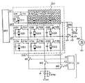
FIG. 15 is a circuit diagram of a photoelectric conversion apparatus showing a third embodiment of the present invention. In order to simplify the explanation, the figure is composed of a total of 9 pixels of 3 × 3. S1-1 to S3-3 are photoelectric conversion elements for receiving visible light and converting them into electrical signals, and T1-1 to T3-3 are signals photoelectrically converted by the photoelectric conversion elements S1-1 to S3-3. This is a switch element for transferring charges to the matrix signal wirings M1 to M3. G1 to G3 are gate drive wirings of switches connected to the shift register (SR1) and connected to the switch elements T1-1 to T3-3. Here, in the circuit diagram of the photoelectric conversion device, the photoelectric conversion elements S1-1 to S3-3 are used as signal output correction circuits. Specifically, the
[0103]
Even in such a circuit configuration, since the X-rays are shielded by the lead plate, the offset component when not irradiated can be similarly removed.
[0104]
(Fourth embodiment)
FIG. 16 is a schematic block diagram showing an example of the entire system using the photoelectric conversion device of the present invention. In FIG. 16,
[0105]
FIG. 17A and FIG. 17B are a schematic configuration diagram and a schematic cross-sectional view, respectively, when the present invention is applied to a photoelectric conversion device for X-ray detection.
[0106]
In FIG. 17, a plurality of pairs of photoelectric conversion elements and TFTs are formed in a
[0107]
Here, a light shielding object (light shielding filter) 7000 having a light transmittance of zero and a light shielding object (light shielding filter) 8000 having a light transmittance of 50% are arranged in the upper left corner of the
[0108]
(Fifth embodiment)
18A and 18B are a schematic configuration diagram and a schematic cross-sectional view, respectively, when the present invention is applied to a photoelectric conversion apparatus for X-ray detection.
[0109]
In FIG. 18, a plurality of pairs of photoelectric conversion elements and TFTs are formed in a
[0110]
In this embodiment, as shown in FIG. 18B, the whole is housed in a
[0111]
In this example, a
[0112]
(Sixth embodiment)
FIGS. 19A and 19B are a schematic configuration diagram and a schematic cross-sectional view, respectively, when the present invention is applied to a photoelectric conversion device for X-ray detection.
[0113]
This embodiment is the same as the fifth embodiment except that the
[0114]
In the present embodiment, offset correction can be performed for each line corresponding to each shift register SR1. Therefore, even when there is a different offset for each line, correction can be performed, and a more uniform output characteristic can be obtained.
[0115]
(Seventh embodiment)
20A and 20B are a schematic configuration diagram and a schematic cross-sectional view, respectively, when the present invention is applied to a photoelectric conversion device for X-ray detection.
[0116]
In this embodiment, a lead plate, which is a shielding member, is provided in a line shape on the photoelectric conversion element at the end where the IC for the integrated circuit for detection is connected instead of the side connected to the shift register SR1. This is different from the sixth embodiment.
[0117]
In the present embodiment, offset correction can be performed for each output line, so output characteristics can be adjusted more easily.
[0118]
In addition to this embodiment, as described in the sixth embodiment, a lead plate as a shielding member may be provided in a line shape along the shift register SR1.
[0119]
In the sixth and seventh embodiments, the shielding member may be provided on the photoelectric conversion element side of the
[0120]
In addition, when a shielding member is provided between the phosphor and the photoelectric conversion element, it is only necessary to block the light emission from the phosphor. Therefore, it is necessary to have black if there is a complementary color component having a sufficient density for the emission color. There is no. For example, when the emission color is green, a red filter with sufficient density (a filter having a red component) may be used.
[0121]
That is, the shielding member may not emit light or substantially emit light in the phosphor even if X-rays are transmitted, and may not be able to sense or substantially sense the photoelectric conversion element even if light is emitted. In addition, when blocking the light emission of the phosphor, it is sufficient that the photoelectric conversion element cannot be sensed or cannot be sensed substantially.
[0122]
In addition, in one form, a shielding member such as a lead plate is provided on the photoelectric conversion element, and the phosphor is not provided on the corresponding element.
[0123]
FIG. 21 is a system configuration diagram showing an example in which the photoelectric conversion device of the present invention is applied to an X-ray diagnostic system.
[0124]
In FIG. 21,
[0125]
Further, this information can be transferred to a remote place by a transmission means such as a
[0126]
When the X-ray diagnostic system is configured as a single substrate by bonding the four sensor substrates in this way, the correction photoelectric conversion elements for correcting the output values of the photoelectric conversion elements are compared among the substrates. It becomes possible to arrange at any one of corners or sides that are not important, or at four corners or at least two sides (using photoelectric conversion elements at four corners or two opposite sides), and the time for scanning the output value There is no special need. Further, by forming at least one correction photoelectric conversion element on each sensor substrate, it is possible to correct the offset and sensitivity between the sensor substrates.
[0127]
Since the corner of the photoelectric conversion device is not a relatively important part, it is preferable to use the corner. When four panels are bonded, if a shielding member such as a filter is arranged at one corner of each panel, it is possible to correct variations among the panels.
[0128]
In addition, by arranging the 0
[0129]
【The invention's effect】
As described above, according to the invention of the present application, a plurality of photoelectric conversion elements arranged two-dimensionally on a substrate are sequentially scanned with drive lines in the X direction, and signal charges are applied to the signal lines in the Y direction. In a photoelectric conversion device that sequentially transfers signals, a filter that has a light transmittance of approximately zero on any photoelectric conversion element, or a lead that can have a zero X-ray transmittance on any photoelectric conversion element By arranging a shielding member represented by a plate, any photoelectric conversion element can be used as a photoelectric conversion element for offset output correction, so that it is not necessary to separately form a correction photoelectric conversion element.
[0130]
As a result, the connection circuit for inputting the output of the external correction photoelectric conversion element to the correction IC and the work thereof become unnecessary, and the yield can be improved and the cost can be reduced.
[0131]
Further, in the photoelectric conversion device, by arranging a filter having a light transmittance m of 0 <m <100% on an arbitrary photoelectric conversion element, it can be used as a sensitivity correction photoelectric conversion element. It is not necessary to separately form a correcting photoelectric conversion element.
[0132]
Also, by using these correction photoelectric conversion elements, it is possible to eliminate variations in sensitivity to the illuminance of the photoelectric conversion elements and in the output when the illuminance is zero, that is, the offset output value.
[0133]
In addition, unlike the case where the correction circuit is arranged independently on the photoelectric conversion device, the circuit is not complicated, and the yield is not reduced in producing the photoelectric conversion device, and the cost is not increased. It is done.
[0134]
Furthermore, when using some photoelectric conversion elements in the two-dimensional photoelectric conversion apparatus composed of multiple pixels as the correction photoelectric conversion elements as in this embodiment, the correction photoelectric conversion elements are arranged on the photoelectric conversion apparatus. Unlike the case where they are arranged independently, it is not necessary to take extra time to read out the correction output. As a result, it is possible to correct the output value of the photoelectric conversion element in a short time, and to obtain a moving image. Is easily possible.
[0135]
Further, when k (for example, four) sensor substrates are bonded together to obtain one substrate, a correction photoelectric conversion element for correcting the output value of the photoelectric conversion element when configuring an X-ray diagnostic system or the like Can be placed at relatively insignificant corners or sides in the substrate, and no time is required to scan the output value.
[0136]
Further, by forming at least one correction photoelectric conversion element on each sensor substrate, it becomes possible to correct the offset and / or sensitivity between the sensor substrates.
[0137]
The present invention can be modified and combined as appropriate within the scope of the gist of the present invention.
[Brief description of the drawings]
FIG. 1 is a schematic circuit diagram for explaining an example of a photoelectric conversion apparatus of the present invention.
2A is a schematic plan view for explaining an example of a correction photoelectric conversion element of the photoelectric conversion apparatus of the present invention, and FIG. 2B is a correction photoelectric conversion shown in FIG. 2A. It is a typical sectional view of a conversion element.
FIG. 3 is a timing chart for explaining an example of driving of the photoelectric conversion device of the present invention.
4 is a schematic plan view showing an example of a pixel configuration of the photoelectric conversion unit in FIG. 11. FIG.
FIG. 5 is a schematic cross-sectional view illustrating an example of a pixel configuration of the photoelectric conversion unit in FIG.
6 is a timing chart illustrating an example of driving of the photoelectric conversion device in FIG. 11. FIG.
FIG. 7 is a schematic plan view showing an example of mounting of a photoelectric conversion device.
FIG. 8 is a schematic plan view showing an example of mounting of a photoelectric conversion device.
FIGS. 9A and 9B are schematic cross-sectional views for explaining an example of an optical sensor, and FIG. 9C is a schematic circuit diagram for explaining an example of a driving method.
FIG. 10 is a schematic cross-sectional view for explaining an example of a structure of a TFT.
FIG. 11 is a schematic circuit diagram illustrating an example of a circuit configuration of a photoelectric conversion apparatus.
FIG. 12 is a schematic circuit diagram for explaining an example of the photoelectric conversion apparatus of the present invention.
13A is a schematic plan view for explaining an example of a correction photoelectric conversion element of the photoelectric conversion device of the present invention, and FIG. 13B is a correction view shown in FIG. 13A. It is a typical sectional view of a photoelectric conversion element.
FIG. 14 is a timing chart for explaining an example of driving of the photoelectric conversion device of the present invention.
FIG. 15 is a schematic circuit diagram for explaining an example of the photoelectric conversion apparatus of the present invention.
FIG. 16 is a schematic circuit diagram for explaining an example of the photoelectric conversion apparatus of the present invention.
FIG. 17A is a schematic plan view for explaining a photoelectric conversion device according to an embodiment of the present invention, and FIG. 17B is a schematic cross-sectional view.
18A is a schematic plan view for explaining a photoelectric conversion device according to an embodiment of the present invention, and FIG. 18B is a schematic cross-sectional view.
19A is a schematic plan view for explaining a photoelectric conversion device according to an embodiment of the present invention, and FIG. 19B is a schematic cross-sectional view.
20A is a schematic plan view showing an example of the configuration of the photoelectric conversion device of the present invention, and FIG. 20B is a schematic cross-sectional view.
FIG. 21 is a schematic system configuration diagram for explaining an example of an X-ray diagnosis (inspection) system having the photoelectric conversion apparatus of the present invention.
[Explanation of symbols]
70 Light blocking filter with 0% light transmittance
80 Shading filter with 50% light transmittance
S11-533 photoelectric conversion element
T11 to T33 Transfer TFT
C11 to C33 capacitors
SR1, SR2 shift register
Claims (13)
該光電変換部上に設けられ、X線を前記光電変換素子が感度を有する波長の光に変換する波長変換体と、を備えた光電変換装置において、
前記複数の光電変換素子のうちの任意の光電変換素子に対応して光の透過率が0%又は実質的に0%である遮へい部材を該任意の光電変換素子と前記波長変換体との間に配置し、
前記任意の光電変換素子から出力されるオフセット補正用出力値と、前記任意の光電変換素子を除いた前記複数の光電変換素子から出力される出力値と、を用いてオフセット補正を行うことを特徴とする光電変換装置。A photoelectric conversion unit having a plurality of photoelectric conversion elements arranged two-dimensionally on a substrate;
A wavelength converter that is provided on the photoelectric conversion unit and converts the X-rays into light having a wavelength at which the photoelectric conversion element has sensitivity ;
A shielding member having a light transmittance of 0% or substantially 0% corresponding to an arbitrary photoelectric conversion element among the plurality of photoelectric conversion elements is disposed between the arbitrary photoelectric conversion element and the wavelength converter. Placed in
Offset correction is performed using an offset correction output value output from the arbitrary photoelectric conversion element and output values output from the plurality of photoelectric conversion elements excluding the arbitrary photoelectric conversion element. A photoelectric conversion device.
Priority Applications (4)
| Application Number | Priority Date | Filing Date | Title |
|---|---|---|---|
| JP26964897A JP4100739B2 (en) | 1996-10-24 | 1997-10-02 | Photoelectric conversion device |
| US08/955,815 US6034406A (en) | 1996-10-24 | 1997-10-22 | Photoelectric conversion apparatus having a shielding member between an arbitrary conversion element and a wavelength converter |
| DE69738043T DE69738043T2 (en) | 1996-10-24 | 1997-10-23 | Photoelectric conversion device with signal correction system |
| EP97308446A EP0838859B1 (en) | 1996-10-24 | 1997-10-23 | Photoelectric conversion apparatus with signal correction capability |
Applications Claiming Priority (3)
| Application Number | Priority Date | Filing Date | Title |
|---|---|---|---|
| JP28234296 | 1996-10-24 | ||
| JP8-282342 | 1996-10-24 | ||
| JP26964897A JP4100739B2 (en) | 1996-10-24 | 1997-10-02 | Photoelectric conversion device |
Publications (2)
| Publication Number | Publication Date |
|---|---|
| JPH10189932A JPH10189932A (en) | 1998-07-21 |
| JP4100739B2 true JP4100739B2 (en) | 2008-06-11 |
Family
ID=26548863
Family Applications (1)
| Application Number | Title | Priority Date | Filing Date |
|---|---|---|---|
| JP26964897A Expired - Fee Related JP4100739B2 (en) | 1996-10-24 | 1997-10-02 | Photoelectric conversion device |
Country Status (4)
| Country | Link |
|---|---|
| US (1) | US6034406A (en) |
| EP (1) | EP0838859B1 (en) |
| JP (1) | JP4100739B2 (en) |
| DE (1) | DE69738043T2 (en) |
Cited By (2)
| Publication number | Priority date | Publication date | Assignee | Title |
|---|---|---|---|---|
| US8364355B2 (en) | 2007-05-30 | 2013-01-29 | Komatsu Ltd. | Driving force controller and driving force control method of working vehicle |
| CN103491284A (en) * | 2012-06-13 | 2014-01-01 | 索尼公司 | Image pickup portion, image pickup unit and image pickup display system |
Families Citing this family (32)
| Publication number | Priority date | Publication date | Assignee | Title |
|---|---|---|---|---|
| JP3805100B2 (en) * | 1997-04-10 | 2006-08-02 | キヤノン株式会社 | Photoelectric conversion device |
| JP3636579B2 (en) * | 1997-11-04 | 2005-04-06 | キヤノン株式会社 | Photoelectric conversion device, method for driving photoelectric conversion device, and system having the photoelectric conversion device |
| JPH11307756A (en) * | 1998-02-20 | 1999-11-05 | Canon Inc | Photoelectric conversion device and radiation reader |
| JP4632383B2 (en) * | 1998-08-31 | 2011-02-16 | キヤノン株式会社 | Semiconductor device used for photoelectric conversion device |
| US6407418B1 (en) | 1998-09-16 | 2002-06-18 | Nec Corporation | Semiconductor device, method of manufacturing the same, image sensor apparatus having the same and image reader having the same |
| US6453008B1 (en) * | 1999-07-29 | 2002-09-17 | Kabushiki Kaisha Toshiba | Radiation detector noise reduction method and radiation detector |
| JP4181703B2 (en) * | 1999-09-02 | 2008-11-19 | キヤノン株式会社 | Photoelectric conversion device |
| DE19945023C2 (en) | 1999-09-20 | 2003-04-24 | Siemens Ag | Areal image detector for electromagnetic rays, especially X-rays |
| JP2002022842A (en) * | 2000-07-07 | 2002-01-23 | Canon Inc | X-ray image detector |
| JP5016746B2 (en) * | 2000-07-28 | 2012-09-05 | キヤノン株式会社 | Imaging apparatus and driving method thereof |
| JP3984808B2 (en) | 2000-09-07 | 2007-10-03 | キヤノン株式会社 | Signal processing apparatus, imaging apparatus using the same, and radiation imaging system |
| US6618604B2 (en) * | 2000-12-28 | 2003-09-09 | Ge Medical Systems Global Technology Company, Llc. | Method and apparatus for correcting the offset induced by field effect transistor photo-conductive effects in a solid state x-ray detector |
| GB2370960A (en) * | 2001-01-05 | 2002-07-10 | Spectral Fusion Technologies L | Partially shielded photodiode array |
| US6960753B2 (en) * | 2001-01-24 | 2005-11-01 | Hewlett-Packard Development Company, L.P. | Photosensor arrays with encoded permanent information |
| JP2003209665A (en) * | 2002-01-16 | 2003-07-25 | Fuji Photo Film Co Ltd | Image reading method and image recording / reading apparatus |
| JP4208491B2 (en) * | 2002-06-11 | 2009-01-14 | キヤノン株式会社 | Imaging device and fingerprint recognition device |
| US7205988B2 (en) * | 2002-07-12 | 2007-04-17 | Toshiba Matsushita Display Technology Co., Ltd. | Display device |
| KR100956338B1 (en) * | 2002-12-11 | 2010-05-06 | 삼성전자주식회사 | Thin Film Transistor Array Substrates for Thin-Ray Detectors |
| US20040217258A1 (en) * | 2003-04-30 | 2004-11-04 | Clugston P. Edward | Solar sensor including reflective element to transform the angular response |
| EP1782477A1 (en) * | 2004-08-20 | 2007-05-09 | Philips Intellectual Property & Standards GmbH | Microelectronic system with a passivation layer |
| US20090096052A1 (en) * | 2006-03-15 | 2009-04-16 | Koninklijke Philips Electronics N.V. | Semiconductor device for radiation detection |
| DE102006021046B4 (en) * | 2006-05-05 | 2013-06-06 | Siemens Aktiengesellschaft | X-ray detector |
| JP5280671B2 (en) * | 2006-12-20 | 2013-09-04 | 富士フイルム株式会社 | Image detector and radiation detection system |
| US20110011455A1 (en) * | 2008-03-11 | 2011-01-20 | Lightwave Power, Inc. | Integrated solar cell with wavelength conversion layers and light guiding and concentrating layers |
| US8384559B2 (en) | 2010-04-13 | 2013-02-26 | Silicon Laboratories Inc. | Sensor device with flexible interface and updatable information store |
| US8384041B2 (en) | 2010-07-21 | 2013-02-26 | Carestream Health, Inc. | Digital radiographic imaging arrays with reduced noise |
| JP6570315B2 (en) * | 2015-05-22 | 2019-09-04 | キヤノン株式会社 | Radiation imaging apparatus and radiation imaging system |
| WO2017089363A1 (en) | 2015-11-26 | 2017-06-01 | Koninklijke Philips N.V. | Dark current compensation |
| JP6808316B2 (en) * | 2015-12-04 | 2021-01-06 | キヤノン株式会社 | Imaging device and imaging system |
| JP6808317B2 (en) * | 2015-12-04 | 2021-01-06 | キヤノン株式会社 | Imaging device and imaging system |
| JP2017220616A (en) * | 2016-06-09 | 2017-12-14 | キヤノン株式会社 | Imaging apparatus and radiation imaging system |
| EP3704514A4 (en) * | 2017-10-30 | 2021-04-21 | Shenzhen Xpectvision Technology Co., Ltd. | DARK NOISE COMPENSATION IN A RADIATION DETECTOR |
Family Cites Families (20)
| Publication number | Priority date | Publication date | Assignee | Title |
|---|---|---|---|---|
| JPS6240862A (en) * | 1985-08-19 | 1987-02-21 | Canon Inc | electronic display and recording device |
| JPS62172859A (en) * | 1986-01-27 | 1987-07-29 | Canon Inc | Image reader |
| JPS62172866A (en) * | 1986-01-27 | 1987-07-29 | Canon Inc | Picture reader |
| US4746793A (en) * | 1986-09-10 | 1988-05-24 | Hewlett-Packard Company | Mask for spectrophotometer photodiode array having a bridge portion that substantially covers each photodiode |
| US4916304A (en) * | 1986-10-07 | 1990-04-10 | Canon Kabushiki Kaisha | Image recording device having a conductive layer formed below a light receiving window |
| US4879470A (en) * | 1987-01-16 | 1989-11-07 | Canon Kabushiki Kaisha | Photoelectric converting apparatus having carrier eliminating means |
| US4866291A (en) * | 1987-06-30 | 1989-09-12 | Canon Kabushiki Kaisha | Photosensor with charge storage unit and switch unit formed on a single-crystal semiconductor film |
| JP2680002B2 (en) * | 1987-11-14 | 1997-11-19 | キヤノン株式会社 | Photoelectric conversion device |
| JP2554119B2 (en) * | 1988-02-26 | 1996-11-13 | 株式会社日立製作所 | Solar radiation sensor for automobile air conditioning |
| US5233442A (en) * | 1989-06-07 | 1993-08-03 | Canon Kabushiki Kaisha | Photosensor and image reading device with improved correction means for signal correction and image reading method |
| JP2929550B2 (en) * | 1989-06-07 | 1999-08-03 | キヤノン株式会社 | Optical sensor and image reading device |
| JP3131218B2 (en) * | 1989-12-06 | 2001-01-31 | トランスウィッチ・コーポレーション | Waveform shaping transversal filter |
| JP2911519B2 (en) * | 1990-02-06 | 1999-06-23 | キヤノン株式会社 | Photoelectric conversion device |
| JPH0423470A (en) * | 1990-05-18 | 1992-01-27 | Fuji Xerox Co Ltd | Image sensor |
| JP2991354B2 (en) * | 1990-11-07 | 1999-12-20 | キヤノン株式会社 | Image reading apparatus and image information processing apparatus having the same |
| US5724152A (en) * | 1993-01-01 | 1998-03-03 | Canon Kabushiki Kaisha | Image reading apparatus and image processing apparatus for reading optical information of visible and non-visible light |
| JP3066944B2 (en) * | 1993-12-27 | 2000-07-17 | キヤノン株式会社 | Photoelectric conversion device, driving method thereof, and system having the same |
| KR0136933B1 (en) * | 1994-05-21 | 1998-04-24 | 문정환 | CDD image device and manufacturing method |
| US5736756A (en) * | 1994-09-29 | 1998-04-07 | Sony Corporation | Solid-state image sensing device with lght shielding film |
| KR100192576B1 (en) * | 1995-11-17 | 1999-06-15 | 윤종용 | Contact image sensor |
-
1997
- 1997-10-02 JP JP26964897A patent/JP4100739B2/en not_active Expired - Fee Related
- 1997-10-22 US US08/955,815 patent/US6034406A/en not_active Expired - Lifetime
- 1997-10-23 EP EP97308446A patent/EP0838859B1/en not_active Expired - Lifetime
- 1997-10-23 DE DE69738043T patent/DE69738043T2/en not_active Expired - Lifetime
Cited By (2)
| Publication number | Priority date | Publication date | Assignee | Title |
|---|---|---|---|---|
| US8364355B2 (en) | 2007-05-30 | 2013-01-29 | Komatsu Ltd. | Driving force controller and driving force control method of working vehicle |
| CN103491284A (en) * | 2012-06-13 | 2014-01-01 | 索尼公司 | Image pickup portion, image pickup unit and image pickup display system |
Also Published As
| Publication number | Publication date |
|---|---|
| EP0838859B1 (en) | 2007-08-22 |
| EP0838859A2 (en) | 1998-04-29 |
| EP0838859A3 (en) | 1999-04-14 |
| DE69738043D1 (en) | 2007-10-04 |
| JPH10189932A (en) | 1998-07-21 |
| US6034406A (en) | 2000-03-07 |
| DE69738043T2 (en) | 2008-05-15 |
Similar Documents
| Publication | Publication Date | Title |
|---|---|---|
| JP4100739B2 (en) | Photoelectric conversion device | |
| JP3636579B2 (en) | Photoelectric conversion device, method for driving photoelectric conversion device, and system having the photoelectric conversion device | |
| JP3066944B2 (en) | Photoelectric conversion device, driving method thereof, and system having the same | |
| JP4307322B2 (en) | Radiation imaging apparatus and radiation imaging system | |
| JP4724313B2 (en) | Imaging apparatus, radiation imaging apparatus, and radiation imaging system using the same | |
| JP4011734B2 (en) | Two-dimensional optical sensor, radiation detection apparatus and radiation diagnostic system using the same | |
| KR100539837B1 (en) | Radiographic image pickup apparatus and method of driving the apparatus | |
| JP3416351B2 (en) | Photoelectric conversion device and driving method thereof, X-ray imaging device using the same, and driving method thereof | |
| JPH09135013A (en) | Photoelectric conversion device and imaging device using the same | |
| JP2004179682A (en) | Radiation imaging device | |
| JP3685446B2 (en) | Photoelectric conversion device | |
| JP4872017B2 (en) | Imaging apparatus, driving method thereof, radiation imaging apparatus, and radiation imaging system using the same | |
| US5912465A (en) | Photoelectric converter | |
| JP3544075B2 (en) | Method for manufacturing photoelectric conversion device | |
| JP5028545B2 (en) | Imaging apparatus, radiation imaging apparatus, and radiation imaging system using the same | |
| JP3560298B2 (en) | Photoelectric conversion device, driving method thereof, and system having the same | |
| JP4921581B2 (en) | Imaging apparatus, radiation imaging apparatus, and radiation imaging system using the same | |
| JP2002158340A (en) | Radiation imaging device, photoelectric conversion device, and radiation imaging system | |
| JP4314255B2 (en) | Conversion device and X-ray detection system | |
| JP3372783B2 (en) | Photoelectric conversion device, driving method thereof, and system having the same | |
| HK1010278A (en) | Photoelectric conversion apparatus with signal correction capability | |
| JP2001309123A (en) | Photoelectric conversion device and imaging device using the same |
Legal Events
| Date | Code | Title | Description |
|---|---|---|---|
| A131 | Notification of reasons for refusal |
Free format text: JAPANESE INTERMEDIATE CODE: A131 Effective date: 20041208 |
|
| A521 | Request for written amendment filed |
Free format text: JAPANESE INTERMEDIATE CODE: A523 Effective date: 20050204 |
|
| A02 | Decision of refusal |
Free format text: JAPANESE INTERMEDIATE CODE: A02 Effective date: 20050330 |
|
| A521 | Request for written amendment filed |
Free format text: JAPANESE INTERMEDIATE CODE: A523 Effective date: 20050516 |
|
| A911 | Transfer to examiner for re-examination before appeal (zenchi) |
Free format text: JAPANESE INTERMEDIATE CODE: A911 Effective date: 20050628 |
|
| A131 | Notification of reasons for refusal |
Free format text: JAPANESE INTERMEDIATE CODE: A131 Effective date: 20050811 |
|
| A521 | Request for written amendment filed |
Free format text: JAPANESE INTERMEDIATE CODE: A523 Effective date: 20051005 |
|
| A912 | Re-examination (zenchi) completed and case transferred to appeal board |
Free format text: JAPANESE INTERMEDIATE CODE: A912 Effective date: 20051209 |
|
| A521 | Request for written amendment filed |
Free format text: JAPANESE INTERMEDIATE CODE: A523 Effective date: 20080214 |
|
| A61 | First payment of annual fees (during grant procedure) |
Free format text: JAPANESE INTERMEDIATE CODE: A61 Effective date: 20080318 |
|
| FPAY | Renewal fee payment (event date is renewal date of database) |
Free format text: PAYMENT UNTIL: 20110328 Year of fee payment: 3 |
|
| R150 | Certificate of patent or registration of utility model |
Free format text: JAPANESE INTERMEDIATE CODE: R150 |
|
| FPAY | Renewal fee payment (event date is renewal date of database) |
Free format text: PAYMENT UNTIL: 20120328 Year of fee payment: 4 |
|
| FPAY | Renewal fee payment (event date is renewal date of database) |
Free format text: PAYMENT UNTIL: 20130328 Year of fee payment: 5 |
|
| FPAY | Renewal fee payment (event date is renewal date of database) |
Free format text: PAYMENT UNTIL: 20140328 Year of fee payment: 6 |
|
| LAPS | Cancellation because of no payment of annual fees |